EP3246770A1 - Digital signal processor, data interaction and conversion device and method, and storage medium - Google Patents
Digital signal processor, data interaction and conversion device and method, and storage medium Download PDFInfo
- Publication number
- EP3246770A1 EP3246770A1 EP15877577.5A EP15877577A EP3246770A1 EP 3246770 A1 EP3246770 A1 EP 3246770A1 EP 15877577 A EP15877577 A EP 15877577A EP 3246770 A1 EP3246770 A1 EP 3246770A1
- Authority
- EP
- European Patent Office
- Prior art keywords
- mode data
- data
- bit width
- format
- different
- Prior art date
- Legal status (The legal status is an assumption and is not a legal conclusion. Google has not performed a legal analysis and makes no representation as to the accuracy of the status listed.)
- Granted
Links
Images


Classifications
-
- G—PHYSICS
- G05—CONTROLLING; REGULATING
- G05B—CONTROL OR REGULATING SYSTEMS IN GENERAL; FUNCTIONAL ELEMENTS OF SUCH SYSTEMS; MONITORING OR TESTING ARRANGEMENTS FOR SUCH SYSTEMS OR ELEMENTS
- G05B19/00—Program-control systems
- G05B19/02—Program-control systems electric
- G05B19/04—Program control other than numerical control, i.e. in sequence controllers or logic controllers
- G05B19/042—Program control other than numerical control, i.e. in sequence controllers or logic controllers using digital processors
-
- G—PHYSICS
- G05—CONTROLLING; REGULATING
- G05B—CONTROL OR REGULATING SYSTEMS IN GENERAL; FUNCTIONAL ELEMENTS OF SUCH SYSTEMS; MONITORING OR TESTING ARRANGEMENTS FOR SUCH SYSTEMS OR ELEMENTS
- G05B2219/00—Program-control systems
- G05B2219/20—Pc systems
- G05B2219/25—Pc structure of the system
- G05B2219/25254—DSP digital signal processor
Definitions
- the present disclosure relates to the technology of Digital Signal Processors (DSPs), and in particular to a DSP, a device and method for data interaction and conversion, and a storage medium.
- DSPs Digital Signal Processors
- DSPs have been widely applied to many fields such as communication, signal and information processing, automatic control, aeronautics and astronautics, medical, and household appliances.
- the DSP may be divided into a common DSP and a dedicated DSP in terms of use.
- the dedicated DSP is designed for specific DSP operations, and is more suitable for special operations, such as digital filtering, convolution and so on.
- FIG. 1 is a traditional device in which a hardware unit performs data interaction and conversion with a dedicated DSP.
- the bit width is N' bits, N' being an integer.
- An input-output bit width interaction and conversion unit 111 in the hardware unit 11 converts data having a bit width of N' bits into data having a bit width of N bits, which is then transmitted on an internal bus 14 of the dedicated DSP 12 in the form of a bit width of N bits; or, the converted data is subjected to direct data interaction with a Random Access Memory (RAM) 13 and the data is stored in the RAM 13 in the form of a bit width of N bits.
- the data structure of the bit width of N bits may refer to the traditional RAM data structure as shown in FIG. 2 .
- the area occupied by the RAM memory in the dedicated DSP increases to N/N' times with respect to the area before data are converted.
- the area of the RAM memory generally occupies more than 50% of the area of the dedicated DSP, thus, in the above traditional device for data interaction and conversion, the area of the DSP increases as the increase of area of the RAM memory, thereby causing an increase in cost.
- the embodiments of the present disclosure provide a DSP, a device and method for data interaction and conversion, and a storage medium, which can solve the problem that the memory area of a dedicated DSP is too large.
- An embodiment of the present disclosure provides a device for data interaction and conversion, which is implemented based on a dedicated DSP and includes: a hardware unit and a dedicated DSP unit, wherein the hardware unit is arranged to perform first mode data interaction with the dedicated DSP unit; and the dedicated DSP unit is arranged to: receive first mode data from the hardware unit, and convert the first mode data into second mode data which has different at least one of bit width and format from the first mode data; and convert the second mode data into third mode data which has different at least one of bit width and format from the second mode data, and perform data computation on the third mode data; or the dedicated DSP unit is arranged to: convert third mode data returned after computation into second mode data which has different at least one of bit width and format from the third mode data; and convert the second mode data into first mode data which has different at least one of bit width and format from the second mode data, and send the first mode data to the hardware unit.
- the dedicated DSP unit is arranged to convert the first mode data into the second mode data which has different at least one of bit width and format from the first mode data, including:
- the dedicated DSP unit is arranged to convert the second mode data into the third mode data which has different at least one of bit width and format from the second mode data, including:
- the dedicated DSP unit is further arranged to store the second mode data converted from the first mode data.
- the dedicated DSP unit includes: a first data conversion unit, a second data conversion unit, an internal bus and a data computation unit; wherein the first data conversion unit is arranged to receive the first mode data from the hardware unit and convert the first mode data into the second mode data which has different at least one of bit width and format from the first mode data; or is arranged to convert the second mode data into the first mode data which has different at least one of bit width and format from the second mode data; the second data conversion unit is arranged to receive the second mode data coming from the first data conversion unit, convert the second mode data into the third mode data which has different at least one of bit width and format from the second mode data and send the third mode data to the internal bus; or is arranged to receive the third mode data from the internal bus, convert the third mode data into the second mode data which has different at least one of bit width and format from the third mode data; the internal bus is arranged to exchange the third mode data with the second data conversion unit and the data computation unit; and the data computation unit is arranged to receive the third mode data
- the dedicated DSP unit further includes a storage unit, and the storage unit is arranged to store the second mode data converted from the first mode data; and the second data conversion unit is arranged to receive the second mode data from the first data conversion unit, or acquire the second mode data from the data storage unit.
- An embodiment of the present disclosure further provides a DSP, which is a dedicated DSP and includes: a first data conversion unit, a second data conversion unit, an internal bus and a data computation unit; wherein the first data conversion unit is arranged to receive first mode data from a hardware unit and convert the first mode data into second mode data which has different at least one of bit width and format from the first mode data; or is arranged to convert second mode data into first mode data which has different at least one of bit width and format from the second mode data; the second data conversion unit is arranged to receive the second mode data from the first data conversion unit, convert the second mode data into third mode data which has different at least one of bit width and format from the second mode data and send the third mode data to the internal bus; or is arranged to receive third mode data from the internal bus, convert the third mode data into the second mode data which has different at least one of bit width and format from the third mode data; the internal bus is arranged to exchange the third mode data with the second data conversion unit and the data computation unit; and the data computation unit is arranged
- the dedicated DSP unit further includes a storage unit, which is arranged to store the second mode data converted from the first mode data; and the second data conversion unit is arranged to receive the second mode data from the first data conversion unit, or acquire the second mode data from the data storage unit.
- An embodiment of the present disclosure further provides a method for data interaction and conversion, which is implemented based on a dedicated DSP and includes:
- converting the first mode data into the second mode data which has different at least one of bit width and format from the first mode data includes:
- converting the second mode data into the third mode data which has different at least one of bit width and format from the second mode data includes:
- the method further includes: storing the second mode data.
- An embodiment of the present disclosure further provides a computer storage medium, which has stored a computer program for executing the above method for data interaction and conversion according to the embodiment of the present disclosure.
- the hardware unit and the dedicated DSP perform interaction based on first mode data.
- the first mode data coming from the hardware unit is converted into second mode data which has different at least one of bit width and format from the first mode data
- the second mode data is converted into third mode data which has different at least one of bit width and format from the second mode data, through the two data conversion units respectively.
- third mode data returned after computation is converted into second mode data which has different at least one of bit width and format from the third mode data
- the second mode data is converted into first mode data which has different at least one of bit width and format from the second mode data and is sent to the hardware unit.
- the first mode data is converted twice inside the dedicated DSP, and the second mode data converted intermediately is then stored, so that the memory area occupied by the data stored in the data storage unit is reduced relatively, thus the area occupied by the dedicated DSP is reduced too, and the problem that how to save the cost of the dedicated DSP in existing technologies is solved.
- interaction is carried out between a hardware unit and a dedicated DSP based on first mode data.
- the first mode data coming from the hardware unit is converted into second mode data which has different at least one of bit width and format from the first mode data
- the second mode data is converted into third mode data which has different at least one of bit width and format from the second mode data
- the third mode data is subjected to data computation, through two data conversion units respectively.
- third mode data returned after computation is converted into second mode data which has different at least one of bit width and format from the third mode data
- the second mode data is converted into first mode data which has different at least one of bit width and format from the second mode data and is sent to the hardware unit.
- the conversion may be the conversion of a data bit width, or may be the conversion of a data format, or may be the conversion of both a data bit width and a data format.
- Fig. 3 is a structure diagram of a DSP provided by an embodiment of the present disclosure, wherein the DSP is a dedicated DSP. As shown in Fig. 3 , the DSP includes: a first data conversion unit 310, a second data conversion unit 330, an internal bus 340 and a data computation unit 350.
- the first data conversion unit 310 may be arranged to receive first mode data from a hardware unit and convert the first mode data into second mode data which has different at least one of bit width and format from the first mode data.
- the first data conversion unit 310 may be also arranged to convert second mode data into first mode data which has different at least one of bit width and format from the second mode data.
- the second data conversion unit 330 may be arranged to receive the second mode data from the first data conversion unit 310, convert the second mode data into third mode data which has different at least one of bit width and format from the second mode data and send the third mode data to the internal bus 340.
- the second data conversion unit 330 may be also arranged to receive third mode data from the internal bus 340, convert the third mode data into the second mode data which has different at least one of bit width and format from the third mode data.
- the internal bus 340 may be arranged to exchange the third mode data with the second data conversion unit 330 and the data computation unit 350.
- the data computation unit 350 may be arranged to receive the third mode data from the internal bus 340 and perform data computation on the third mode data.
- the data computation unit 350 may be also arranged to return the computed third mode data to the internal bus 340.
- the first data conversion unit 310 may be arranged to convert the first mode data into the second mode data which has different at least one of bit width and format from the first mode data, including: the first data conversion unit 310 is arranged to convert the first mode data into the second mode data which has a different bit width from the first mode data, or, convert the first mode data into the second mode data which has a different format from the first mode data, or, convert the first mode data into the second mode data which has different bit width and format from the first mode data.
- the first data conversion unit 310 may be arranged to convert the second mode data into the first mode data which has different at least one of bit width and format from the second mode data, including: the first data conversion unit 310 is arranged to convert the second mode data into the first mode data which has a different bit width from the second mode data, or, convert the second mode data into the first mode data which has a different format from the second mode data, or, convert the second mode data into the first mode data which has different bit width and format from the second mode data.
- the bit width of the second mode data is greater than or equal to the bit width of the first mode data.
- the second data conversion unit 330 may be arranged to convert the second mode data into the third mode data which has different at least one of bit width and format from the second mode data, including: the second data conversion unit 330 is arranged to convert the second mode data into the third mode data which has a different bit width from the second mode data, or, convert the second mode data into the third mode data which has a different format from the second mode data, or, convert the second mode data into the third mode data which has different bit width and format from the second mode data.
- the second data conversion unit 330 may be arranged to convert the third mode data into the second mode data which has different at least one of bit width and format from the third mode data, including: the second data conversion unit 330 is arranged to convert the third mode data into the second mode data which has a different bit width from the third mode data, or, convert the third mode data into the second mode data which has a different format from the third mode data, or, convert the third mode data into the second mode data which has different bit width and format from the third mode data.
- the bit width of the third mode data is greater than or equal to the bit width of the second mode data.
- the DSP unit further includes a storage unit 320, which is arranged to store the second mode data converted from the first mode data.
- the second data conversion unit 330 is arranged to receive the second mode data from the first data conversion unit 310, or acquire the second mode data from the data storage unit 320.
- the data storage unit 320 may be an RAM.
- Fig. 4 is a structure diagram of a device for data interaction and conversion of an embodiment of the present disclosure.
- the device is implemented based on a dedicated DSP.
- the device includes: a hardware unit 410 and a dedicated DSP 420.
- the hardware unit 410 is arranged to perform first mode data interaction with the dedicated DSP unit 420.
- the dedicated DSP unit 420 may be arranged to: receive first mode data from the hardware unit 410, and convert the first mode data into second mode data which has different at least one of bit width and format from the first mode data; convert the second mode data into third mode data which has different at least one of bit width and format from the second mode data, and perform data computation on the third mode data.
- the dedicated DSP unit 420 may also be arranged to: convert third mode data returned after computation into second mode data which has different at least one of bit width and format from the third mode data; and convert the second mode data into first mode data which has different at least one of bit width and format from the second mode data, and send the first mode data to the hardware unit 410.
- the dedicated DSP unit 420 may include: a first data conversion unit 421, a second data conversion unit 423, an internal bus 424 and a data computation unit 425.
- the first data conversion unit 421 may be arranged to receive first mode data from the hardware unit 410 and convert the first mode data into second mode data which has different at least one of bit width and format from the first mode data.
- the first data conversion unit 421 may be also arranged to convert second mode data into first mode data which has different at least one of bit width and format from the second mode data;
- the second data conversion unit 423 may be arranged to receive the second mode data from the first data conversion unit 421, convert the second mode data into third mode data which has different at least one of bit width and format from the second mode data and send the third mode data to the internal bus 424.
- the second data conversion unit 423 may be also arranged to receive third mode data from the internal bus 424, convert the third mode data into second mode data which has different at least one of bit width and format from the third mode data.
- the internal bus 424 may be arranged to exchange the third mode data with the second data conversion unit 423 and the data computation unit 425.
- the data computation unit 425 may be arranged to receive the third mode data from the internal bus 424 and perform data computation on the third mode data.
- the data computation unit 425 may be also arranged to return the computed third mode data to the internal bus 424.
- the dedicated DSP unit 420 may be arranged to convert the first mode data into the second mode data which has different at least one of bit width and format from the first mode data, including: the dedicated DSP unit 420 is arranged to convert the first mode data into the second mode data which has a different bit width from the first mode data, or, convert the first mode data into the second mode data which has a different format from the first mode data, or, convert the first mode data into the second mode data which has different bit width and format from the first mode data.
- the dedicated DSP unit 420 may be arranged to convert the second mode data into the first mode data which has different at least one of bit width and format from the second mode data, including: the dedicated DSP unit 420 is arranged to convert the second mode data into the first mode data which has a different bit width from the second mode data, or, convert the second mode data into the first mode data which has a different format from the second mode data, or, convert the second mode data into the first mode data which has different bit width and format from the second mode data.
- the bit width of the second mode data is greater than or equal to the bit width of the first mode data.
- the dedicated DSP unit 420 may be arranged to convert the second mode data into the third mode data which has different at least one of bit width and format from the second mode data, including: the dedicated DSP unit 420 is arranged to convert the second mode data into the third mode data which has a different bit width from the second mode data, or, convert the second mode data into the third mode data which has a different format from the second mode data, or, convert the second mode data into the third mode data which has different bit width and format from the second mode data.
- the dedicated DSP unit 420 may be arranged to convert the third mode data into the second mode data which has different at least one of bit width and format from the third mode data, including: the dedicated DSP unit 420 is arranged to convert the third mode data into the second mode data which has a different bit width from the third mode data, or, convert the third mode data into the second mode data which has a different format from the third mode data, or, convert the third mode data into the second mode data which has different bit width and format from the third mode data.
- the bit width of the third mode data is greater than or equal to the bit width of the second mode data.
- the dedicated DSP unit may further include a storage unit 422, which is arranged to store the second mode data converted from the first mode data;
- the second data conversion unit 423 is arranged to receive the second mode data from the first data conversion unit 421, or acquire the second mode data from the data storage unit 422.
- the data storage unit 422 may be an RAM.
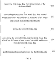
- Fig. 5 is an implementation flowchart of a method for data interaction and conversion of an embodiment of the present disclosure. The method is implemented based on a dedicated DSP. As shown in Fig 5 , in conjunction with the above embodiment and Fig. 4 , the method includes the steps below.
- Step 501 first mode data is received from the external of the dedicated DSP.
- interaction is carried out between the hardware unit 410 and the first data conversion unit 421 of the dedicated DSP unit 420 based on the first mode data.
- Step 502 the received first mode data is converted into second mode data which has different at least one of bit width and format from the first mode data.
- the conversion refers to the conversion of a data bit width, or, the conversion of a data format, or, the conversion of both a data bit width and a format.
- the at least one of bit width and format of the received first mode data may be converted into a different at least one of bit width and format by the first data conversion unit 421, the converted data being the second mode data.
- converting the at least one of bit width and format of the first mode data into a different at least one of bit width and format is: converting the original bit width of N' bits of the first mode data into a first bit width of N" bits, N' and N" being integers; or, converting the original format of the first mode data into a first format, for example, the original format is an integer, the first format is a block floating-point number; or, converting the original bit width of N' bits and the original format of the first mode data into the first bit width of N" bits and the first format respectively, N' and N" being integers.
- the first mode data may be converted into the second mode data through three data conversion modes in the first data conversion unit, that is, bit width conversion only, data format conversion only, both bit width conversion and data format conversion.
- Step 503 the second mode data is stored.
- the converted second mode data is stored by the data storage unit 422.
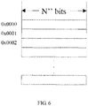
- Fig. 6 is a schematic diagram of data structure of a data storage unit in an embodiment of the present disclosure.
- Step 502 under the condition that the original bit width of N' bits of the first mode data is converted into the first bit width of N" bits, as shown in Fig. 6 , the bit width of the data storage unit is N" bits.
- this step may be omitted.
- Step 504 the second mode data is converted into third mode data which has different at least one of bit width and format from the second mode data.
- the at least one of bit width and format of the second mode data may be converted into a different at least one of bit width and format by the second data conversion unit 423, the converted data being the third mode data.
- converting the at least one of bit width and format of the second mode data into a different at least one of bit width and format is: converting the first bit width of N" bits of the second mode data into a second bit width of N bits, N" and N being integers; or, converting the first format of the second mode data into a second format; or, converting the first bit width of N" bits and the first format of the second mode data into the second bit width of N bits and the second format respectively, N" and N being integers.
- the second bit width of N bits of the third mode data is greater than the first bit width of N" bits of the second mode data.
- the second mode data may be converted into the third mode data through three data conversion modes in the second data conversion unit, that is, bit width conversion only, data format conversion only, both bit width conversion and data format conversion.
- Step 505 data computation is performed on the third mode data.
- the second data conversion unit 423 exchanges third mode data with the internal bus 424, the internal bus 424 exchanges the third mode data with the data computation unit 425.
- the data computation unit 425 performs data computation on the third mode data. Since the third mode data of the data computation unit 425 is not subjected to any conversion, the bit width and format of the third mode data are not changed.
- the method for data interaction and conversion of the embodiment of the present disclosure may include reverse operations of Step 501 to Step 505, including: converting third mode data returned after computation into second mode data which has different at least one of bit width and format from the third mode data; converting the second mode data into first mode data which has different at least one of bit width and format from the second mode data; then, sending the converted first mode data to the hardware unit external to the dedicated DSP.
- the bit with of the second mode data in the data storage unit is N" bits.
- the value of N" is between N and N', N and N' meet ⁇ N ′ 8 ⁇ ⁇ 8 , ⁇ N ′ 8 ⁇ being rounded up to an integer, N', N" and N being integers.
- the first mode data is converted twice inside the dedicated DSP, the bit width of the second mode data in the data storage unit is reduced relative to existing technologies.
- the area of the data storage unit of the embodiment of the present disclosure is reduced, thus, the area occupied by the dedicated DSP of the embodiment of the present disclosure is reduced. Accordingly, according to the embodiment of the present disclosure, the cost of the dedicated DSP can be reduced, thereby achieving the effect of saving cost.
- the dedicated DSP unit in the device for data interaction and conversion proposed in the embodiment of the present disclosure may be a DSP.
- the hardware unit may be a processor, or may be a specific logic circuit.
- the processor may be a Central Processing Unit (CPU), a Micro Processor Unit (MPU) or a Field Programmable Gate Array (FPGA), etc.
- the software function module may be stored in a computer readable storage medium.
- This computer software product is stored in a storage medium, including a number of instructions that enable a computer device (which might be a computer, a server or a network device, etc.) to execute part or the entirety of the method described in each embodiment of the present disclosure.
- the aforementioned storage medium includes: a USB flash disk, a mobile hard disk, a Read-Only Memory (ROM), a diskette or compact disc and various mediums capable of storing program codes.
- ROM Read-Only Memory
- the embodiment of the present disclosure is not limited to any specific combination of hardware and software.
- an embodiment of the present disclosure further provides a computer storage medium, which stores a computer program that is arranged to execute the above method for data interaction and conversion as described in the embodiment of the present disclosure.
Landscapes
- Physics & Mathematics (AREA)
- General Physics & Mathematics (AREA)
- Engineering & Computer Science (AREA)
- Automation & Control Theory (AREA)
- Bus Control (AREA)
- Compression, Expansion, Code Conversion, And Decoders (AREA)
Description
- The present disclosure relates to the technology of Digital Signal Processors (DSPs), and in particular to a DSP, a device and method for data interaction and conversion, and a storage medium.
- With the development of microelectronic technologies and computer technologies, DSPs have been widely applied to many fields such as communication, signal and information processing, automatic control, aeronautics and astronautics, medical, and household appliances. The DSP may be divided into a common DSP and a dedicated DSP in terms of use. The dedicated DSP is designed for specific DSP operations, and is more suitable for special operations, such as digital filtering, convolution and so on.
-
FIG. 1 is a traditional device in which a hardware unit performs data interaction and conversion with a dedicated DSP. As shown inFIG. 1 , in thehardware unit 11, the bit width is N' bits, N' being an integer. An input-output bit width interaction andconversion unit 111 in thehardware unit 11 converts data having a bit width of N' bits into data having a bit width of N bits, which is then transmitted on an internal bus 14 of thededicated DSP 12 in the form of a bit width of N bits; or, the converted data is subjected to direct data interaction with a Random Access Memory (RAM) 13 and the data is stored in theRAM 13 in the form of a bit width of N bits. The data structure of the bit width of N bits may refer to the traditional RAM data structure as shown inFIG. 2 . - Thus, it can be seen that in the above traditional device in which a hardware unit performs data interaction and conversion with a dedicated DSP, the area occupied by the RAM memory in the dedicated DSP increases to N/N' times with respect to the area before data are converted. Meanwhile, considering that the area of the RAM memory generally occupies more than 50% of the area of the dedicated DSP, thus, in the above traditional device for data interaction and conversion, the area of the DSP increases as the increase of area of the RAM memory, thereby causing an increase in cost.
- Since dedicated DSPs with lower cost are still selected to be used in many application fields at present, how to save the area of the dedicated DSP has become a technical problem to be solved in related art.
- In view of this, the embodiments of the present disclosure provide a DSP, a device and method for data interaction and conversion, and a storage medium, which can solve the problem that the memory area of a dedicated DSP is too large.
- Accordingly, the technical scheme of the embodiments of the present disclosure is realized as follows.
- An embodiment of the present disclosure provides a device for data interaction and conversion, which is implemented based on a dedicated DSP and includes: a hardware unit and a dedicated DSP unit, wherein
the hardware unit is arranged to perform first mode data interaction with the dedicated DSP unit; and
the dedicated DSP unit is arranged to: receive first mode data from the hardware unit, and convert the first mode data into second mode data which has different at least one of bit width and format from the first mode data; and convert the second mode data into third mode data which has different at least one of bit width and format from the second mode data, and perform data computation on the third mode data; or
the dedicated DSP unit is arranged to: convert third mode data returned after computation into second mode data which has different at least one of bit width and format from the third mode data; and convert the second mode data into first mode data which has different at least one of bit width and format from the second mode data, and send the first mode data to the hardware unit. - In the above scheme, the dedicated DSP unit is arranged to convert the first mode data into the second mode data which has different at least one of bit width and format from the first mode data, including:
- the dedicated DSP unit is arranged to convert the first mode data into the second mode data which has a different bit width from the first mode data; or, the dedicated DSP unit is arranged to convert the first mode data into the second mode data which has a different format from the first mode data; or, the dedicated DSP unit is arranged to convert the first mode data into the second mode data which has different bit width and format from the first mode data;
- the dedicated DSP unit is arranged to convert the second mode data into the first mode data which has a different bit width from the second mode data; or, the dedicated DSP unit is arranged to convert the second mode data into the first mode data which has a different format from the second mode data; or, the dedicated DSP unit is arranged to convert the second mode data into the first mode data which has different bit width and format from the second mode data;
- wherein the bit width of the second mode data is greater than or equal to the bit width of the first mode data.
- In the above scheme, the dedicated DSP unit is arranged to convert the second mode data into the third mode data which has different at least one of bit width and format from the second mode data, including:
- the dedicated DSP unit is arranged to convert the second mode data into the third mode data which has a different bit width from the second mode data; or, the dedicated DSP unit is arranged to convert the second mode data into the third mode data which has a different format from the second mode data; or, the dedicated DSP unit is arranged to convert the second mode data into the third mode data which has different bit width and format from the second mode data;
- the dedicated DSP unit is arranged to convert the third mode data into the second mode data which has a different bit width from the third mode data; or, the dedicated DSP unit is arranged to convert the third mode data into the second mode data which has a different format from the third mode data; or, the dedicated DSP unit is arranged to convert the third mode data into the second mode data which has different bit width and format from the third mode data;
- In the above scheme, the dedicated DSP unit is further arranged to store the second mode data converted from the first mode data.
- In the above scheme, the dedicated DSP unit includes: a first data conversion unit, a second data conversion unit, an internal bus and a data computation unit; wherein
the first data conversion unit is arranged to receive the first mode data from the hardware unit and convert the first mode data into the second mode data which has different at least one of bit width and format from the first mode data; or is arranged to convert the second mode data into the first mode data which has different at least one of bit width and format from the second mode data;
the second data conversion unit is arranged to receive the second mode data coming from the first data conversion unit, convert the second mode data into the third mode data which has different at least one of bit width and format from the second mode data and send the third mode data to the internal bus; or is arranged to receive the third mode data from the internal bus, convert the third mode data into the second mode data which has different at least one of bit width and format from the third mode data;
the internal bus is arranged to exchange the third mode data with the second data conversion unit and the data computation unit; and
the data computation unit is arranged to receive the third mode data coming from the internal bus and perform the data computation on the third mode data, and is further arranged to return the computed third mode data to the internal bus. - In the above scheme, the dedicated DSP unit further includes a storage unit, and the storage unit is arranged to store the second mode data converted from the first mode data; and
the second data conversion unit is arranged to receive the second mode data from the first data conversion unit, or acquire the second mode data from the data storage unit. - An embodiment of the present disclosure further provides a DSP, which is a dedicated DSP and includes: a first data conversion unit, a second data conversion unit, an internal bus and a data computation unit; wherein
the first data conversion unit is arranged to receive first mode data from a hardware unit and convert the first mode data into second mode data which has different at least one of bit width and format from the first mode data; or is arranged to convert second mode data into first mode data which has different at least one of bit width and format from the second mode data;
the second data conversion unit is arranged to receive the second mode data from the first data conversion unit, convert the second mode data into third mode data which has different at least one of bit width and format from the second mode data and send the third mode data to the internal bus; or is arranged to receive third mode data from the internal bus, convert the third mode data into the second mode data which has different at least one of bit width and format from the third mode data;
the internal bus is arranged to exchange the third mode data with the second data conversion unit and the data computation unit; and
the data computation unit is arranged to receive the third mode data from the internal bus and perform data computation on the third mode data, and is further arranged to return the computed third mode data to the internal bus. - In the above scheme, the dedicated DSP unit further includes a storage unit, which is arranged to store the second mode data converted from the first mode data; and
the second data conversion unit is arranged to receive the second mode data from the first data conversion unit, or acquire the second mode data from the data storage unit. - An embodiment of the present disclosure further provides a method for data interaction and conversion, which is implemented based on a dedicated DSP and includes:
- receiving first mode data from external of the dedicated DSP;
- converting the first mode data into second mode data which has different at least one of bit width and format from the first mode data; and
- converting the second mode data into third mode data which has different at least one of bit width and format from the second mode data, and performing data computation on the third mode data;
or, - converting third mode data returned after computation into second mode data which has different at least one of bit width and format from the third mode data;
- converting the second mode data into first mode data which has different at least one of bit width and format from the second mode data; and
- sending the first mode data to external of the dedicated DSP.
- In the above scheme, converting the first mode data into the second mode data which has different at least one of bit width and format from the first mode data includes:
- converting the first mode data into the second mode data which has a different bit width from the first mode data; or, converting the first mode data into the second mode data which has a different format from the first mode data; or, converting the first mode data into the second mode data which has different bit width and format from the first mode data;
- converting the second mode data into the first mode data which has a different bit width from the second mode data; or, converting the second mode data into the first mode data which has a different format from the second mode data; or, converting the second mode data into the first mode data which has different bit width and format from the second mode data;
- In the above scheme, converting the second mode data into the third mode data which has different at least one of bit width and format from the second mode data includes:
- converting the second mode data into the third mode data which has a different bit width from the second mode data; or, converting the second mode data into the third mode data which has a different format from the second mode data; or, converting the second mode data into the third mode data which has different bit width and format from the second mode data;
- converting the third mode data into the second mode data which has different at least one of bit width and format from the third mode data includes:
- converting the third mode data into the second mode data which has a different bit width from the third mode data; or, converting the third mode data into the second mode data which has a different format from the third mode data; or, converting the third mode data into the second mode data which has different bit width and format from the third mode data;
- wherein the bit width of the third mode data is greater than or equal to the bit width of the second mode data.
- In the above scheme, after converting the received first mode data into the second mode data which has different at least one of bit width and format from the first mode data, the method further includes: storing the second mode data.
- An embodiment of the present disclosure further provides a computer storage medium, which has stored a computer program for executing the above method for data interaction and conversion according to the embodiment of the present disclosure.
- For the DSP, the device and method for data interaction and conversion, and the storage medium provided by the embodiments of the present disclosure, the hardware unit and the dedicated DSP perform interaction based on first mode data. For the dedicated DSP, the first mode data coming from the hardware unit is converted into second mode data which has different at least one of bit width and format from the first mode data, and the second mode data is converted into third mode data which has different at least one of bit width and format from the second mode data, through the two data conversion units respectively. Or, vice versa, third mode data returned after computation is converted into second mode data which has different at least one of bit width and format from the third mode data, and the second mode data is converted into first mode data which has different at least one of bit width and format from the second mode data and is sent to the hardware unit. Thus, according to the embodiments of the present disclosure, the first mode data is converted twice inside the dedicated DSP, and the second mode data converted intermediately is then stored, so that the memory area occupied by the data stored in the data storage unit is reduced relatively, thus the area occupied by the dedicated DSP is reduced too, and the problem that how to save the cost of the dedicated DSP in existing technologies is solved.
-
-
Fig. 1 is a structure diagram of a traditional device in which a hardware unit performs data interaction and conversion with a dedicated DSP; -
Fig. 2 is a schematic diagram of data structure in a traditional RAM memory; -
Fig. 3 is a structure diagram of a DSP provided by an embodiment of the present disclosure; -
Fig. 4 is a structure diagram of a device for data interaction and conversion of an embodiment of the present disclosure; -
Fig. 5 is an implementation flowchart of a method for data interaction and conversion of an embodiment of the present disclosure; and -
Fig. 6 is a schematic diagram of data structure of a data storage unit in an embodiment of the present disclosure. - In the embodiments of the present disclosure, interaction is carried out between a hardware unit and a dedicated DSP based on first mode data. In the dedicated DSP, the first mode data coming from the hardware unit is converted into second mode data which has different at least one of bit width and format from the first mode data, the second mode data is converted into third mode data which has different at least one of bit width and format from the second mode data, and the third mode data is subjected to data computation, through two data conversion units respectively. Or, vice versa, third mode data returned after computation is converted into second mode data which has different at least one of bit width and format from the third mode data, and the second mode data is converted into first mode data which has different at least one of bit width and format from the second mode data and is sent to the hardware unit.
- Here, the conversion may be the conversion of a data bit width, or may be the conversion of a data format, or may be the conversion of both a data bit width and a data format.
- The present disclosure is described below in further detail in conjunction with accompanying drawings and specific embodiments.
-
Fig. 3 is a structure diagram of a DSP provided by an embodiment of the present disclosure, wherein the DSP is a dedicated DSP. As shown inFig. 3 , the DSP includes: a firstdata conversion unit 310, a seconddata conversion unit 330, aninternal bus 340 and adata computation unit 350. - The first
data conversion unit 310 may be arranged to receive first mode data from a hardware unit and convert the first mode data into second mode data which has different at least one of bit width and format from the first mode data. The firstdata conversion unit 310 may be also arranged to convert second mode data into first mode data which has different at least one of bit width and format from the second mode data. - The second
data conversion unit 330 may be arranged to receive the second mode data from the firstdata conversion unit 310, convert the second mode data into third mode data which has different at least one of bit width and format from the second mode data and send the third mode data to theinternal bus 340. The seconddata conversion unit 330 may be also arranged to receive third mode data from theinternal bus 340, convert the third mode data into the second mode data which has different at least one of bit width and format from the third mode data. - The
internal bus 340 may be arranged to exchange the third mode data with the seconddata conversion unit 330 and thedata computation unit 350. - The
data computation unit 350 may be arranged to receive the third mode data from theinternal bus 340 and perform data computation on the third mode data. Thedata computation unit 350 may be also arranged to return the computed third mode data to theinternal bus 340. - The first
data conversion unit 310 may be arranged to convert the first mode data into the second mode data which has different at least one of bit width and format from the first mode data, including: the firstdata conversion unit 310 is arranged to convert the first mode data into the second mode data which has a different bit width from the first mode data, or, convert the first mode data into the second mode data which has a different format from the first mode data, or, convert the first mode data into the second mode data which has different bit width and format from the first mode data. - The first
data conversion unit 310 may be arranged to convert the second mode data into the first mode data which has different at least one of bit width and format from the second mode data, including: the firstdata conversion unit 310 is arranged to convert the second mode data into the first mode data which has a different bit width from the second mode data, or, convert the second mode data into the first mode data which has a different format from the second mode data, or, convert the second mode data into the first mode data which has different bit width and format from the second mode data. - The bit width of the second mode data is greater than or equal to the bit width of the first mode data.
- The second
data conversion unit 330 may be arranged to convert the second mode data into the third mode data which has different at least one of bit width and format from the second mode data, including: the seconddata conversion unit 330 is arranged to convert the second mode data into the third mode data which has a different bit width from the second mode data, or, convert the second mode data into the third mode data which has a different format from the second mode data, or, convert the second mode data into the third mode data which has different bit width and format from the second mode data. - The second
data conversion unit 330 may be arranged to convert the third mode data into the second mode data which has different at least one of bit width and format from the third mode data, including: the seconddata conversion unit 330 is arranged to convert the third mode data into the second mode data which has a different bit width from the third mode data, or, convert the third mode data into the second mode data which has a different format from the third mode data, or, convert the third mode data into the second mode data which has different bit width and format from the third mode data. - The bit width of the third mode data is greater than or equal to the bit width of the second mode data.
- The DSP unit further includes a
storage unit 320, which is arranged to store the second mode data converted from the first mode data. - Correspondingly, the second
data conversion unit 330 is arranged to receive the second mode data from the firstdata conversion unit 310, or acquire the second mode data from thedata storage unit 320. - Here, the
data storage unit 320 may be an RAM. -
Fig. 4 is a structure diagram of a device for data interaction and conversion of an embodiment of the present disclosure. The device is implemented based on a dedicated DSP. The device includes: ahardware unit 410 and adedicated DSP 420. - The
hardware unit 410 is arranged to perform first mode data interaction with thededicated DSP unit 420. - The
dedicated DSP unit 420 may be arranged to: receive first mode data from thehardware unit 410, and convert the first mode data into second mode data which has different at least one of bit width and format from the first mode data; convert the second mode data into third mode data which has different at least one of bit width and format from the second mode data, and perform data computation on the third mode data. Thededicated DSP unit 420 may also be arranged to: convert third mode data returned after computation into second mode data which has different at least one of bit width and format from the third mode data; and convert the second mode data into first mode data which has different at least one of bit width and format from the second mode data, and send the first mode data to thehardware unit 410. - The
dedicated DSP unit 420 may include: a firstdata conversion unit 421, a seconddata conversion unit 423, aninternal bus 424 and adata computation unit 425. - The first
data conversion unit 421 may be arranged to receive first mode data from thehardware unit 410 and convert the first mode data into second mode data which has different at least one of bit width and format from the first mode data. The firstdata conversion unit 421 may be also arranged to convert second mode data into first mode data which has different at least one of bit width and format from the second mode data; - The second
data conversion unit 423 may be arranged to receive the second mode data from the firstdata conversion unit 421, convert the second mode data into third mode data which has different at least one of bit width and format from the second mode data and send the third mode data to theinternal bus 424. The seconddata conversion unit 423 may be also arranged to receive third mode data from theinternal bus 424, convert the third mode data into second mode data which has different at least one of bit width and format from the third mode data. - The
internal bus 424 may be arranged to exchange the third mode data with the seconddata conversion unit 423 and thedata computation unit 425. - The
data computation unit 425 may be arranged to receive the third mode data from theinternal bus 424 and perform data computation on the third mode data. Thedata computation unit 425 may be also arranged to return the computed third mode data to theinternal bus 424. - The
dedicated DSP unit 420 may be arranged to convert the first mode data into the second mode data which has different at least one of bit width and format from the first mode data, including: thededicated DSP unit 420 is arranged to convert the first mode data into the second mode data which has a different bit width from the first mode data, or, convert the first mode data into the second mode data which has a different format from the first mode data, or, convert the first mode data into the second mode data which has different bit width and format from the first mode data. - The
dedicated DSP unit 420 may be arranged to convert the second mode data into the first mode data which has different at least one of bit width and format from the second mode data, including: thededicated DSP unit 420 is arranged to convert the second mode data into the first mode data which has a different bit width from the second mode data, or, convert the second mode data into the first mode data which has a different format from the second mode data, or, convert the second mode data into the first mode data which has different bit width and format from the second mode data. - The bit width of the second mode data is greater than or equal to the bit width of the first mode data.
- The
dedicated DSP unit 420 may be arranged to convert the second mode data into the third mode data which has different at least one of bit width and format from the second mode data, including: thededicated DSP unit 420 is arranged to convert the second mode data into the third mode data which has a different bit width from the second mode data, or, convert the second mode data into the third mode data which has a different format from the second mode data, or, convert the second mode data into the third mode data which has different bit width and format from the second mode data. - The
dedicated DSP unit 420 may be arranged to convert the third mode data into the second mode data which has different at least one of bit width and format from the third mode data, including: thededicated DSP unit 420 is arranged to convert the third mode data into the second mode data which has a different bit width from the third mode data, or, convert the third mode data into the second mode data which has a different format from the third mode data, or, convert the third mode data into the second mode data which has different bit width and format from the third mode data. - The bit width of the third mode data is greater than or equal to the bit width of the second mode data.
- The dedicated DSP unit may further include a
storage unit 422, which is arranged to store the second mode data converted from the first mode data; - Correspondingly, the second
data conversion unit 423 is arranged to receive the second mode data from the firstdata conversion unit 421, or acquire the second mode data from thedata storage unit 422. - Here, the
data storage unit 422 may be an RAM. -
Fig. 5 is an implementation flowchart of a method for data interaction and conversion of an embodiment of the present disclosure. The method is implemented based on a dedicated DSP. As shown inFig 5 , in conjunction with the above embodiment andFig. 4 , the method includes the steps below. - Step 501: first mode data is received from the external of the dedicated DSP.
- Here, interaction is carried out between the
hardware unit 410 and the firstdata conversion unit 421 of thededicated DSP unit 420 based on the first mode data. - Step 502: the received first mode data is converted into second mode data which has different at least one of bit width and format from the first mode data.
- In
Step 502, the conversion refers to the conversion of a data bit width, or, the conversion of a data format, or, the conversion of both a data bit width and a format. The at least one of bit width and format of the received first mode data may be converted into a different at least one of bit width and format by the firstdata conversion unit 421, the converted data being the second mode data. - Here, converting the at least one of bit width and format of the first mode data into a different at least one of bit width and format is: converting the original bit width of N' bits of the first mode data into a first bit width of N" bits, N' and N" being integers; or, converting the original format of the first mode data into a first format, for example, the original format is an integer, the first format is a block floating-point number; or, converting the original bit width of N' bits and the original format of the first mode data into the first bit width of N" bits and the first format respectively, N' and N" being integers.
- In the above embodiment, the first bit width of N" bits of the second mode data is greater than or equal to the original bit width of N' bits of the first mode data, for example, when N' is 10, N" may be 12; thus, the above condition meets N">=N'.
- That is to say, the first mode data may be converted into the second mode data through three data conversion modes in the first data conversion unit, that is, bit width conversion only, data format conversion only, both bit width conversion and data format conversion.
- Step 503: the second mode data is stored.
- Here, the converted second mode data is stored by the
data storage unit 422. -
Fig. 6 is a schematic diagram of data structure of a data storage unit in an embodiment of the present disclosure. - In
Step 502, under the condition that the original bit width of N' bits of the first mode data is converted into the first bit width of N" bits, as shown inFig. 6 , the bit width of the data storage unit is N" bits. - In actual application, this step may be omitted.
- Step 504: the second mode data is converted into third mode data which has different at least one of bit width and format from the second mode data.
- In
Step 504, the at least one of bit width and format of the second mode data may be converted into a different at least one of bit width and format by the seconddata conversion unit 423, the converted data being the third mode data. - Here, converting the at least one of bit width and format of the second mode data into a different at least one of bit width and format is: converting the first bit width of N" bits of the second mode data into a second bit width of N bits, N" and N being integers; or, converting the first format of the second mode data into a second format; or, converting the first bit width of N" bits and the first format of the second mode data into the second bit width of N bits and the second format respectively, N" and N being integers.
- Here, the second bit width of N bits of the third mode data is greater than the first bit width of N" bits of the second mode data.
- In the above process, the value of N" is between N and N', N and N' meet:

- That is to say, the second mode data may be converted into the third mode data through three data conversion modes in the second data conversion unit, that is, bit width conversion only, data format conversion only, both bit width conversion and data format conversion.
- Step 505: data computation is performed on the third mode data.
- The second
data conversion unit 423 exchanges third mode data with theinternal bus 424, theinternal bus 424 exchanges the third mode data with thedata computation unit 425. Thedata computation unit 425 performs data computation on the third mode data. Since the third mode data of thedata computation unit 425 is not subjected to any conversion, the bit width and format of the third mode data are not changed. - In actual application, the method for data interaction and conversion of the embodiment of the present disclosure may include reverse operations of
Step 501 to Step 505, including: converting third mode data returned after computation into second mode data which has different at least one of bit width and format from the third mode data; converting the second mode data into first mode data which has different at least one of bit width and format from the second mode data; then, sending the converted first mode data to the hardware unit external to the dedicated DSP. - From the above embodiments it can be seen that, in the modes of converting bit width only and converting bit width and data format simultaneously, the bit with of the second mode data in the data storage unit is N" bits. Relative to the bit width N of the RAM memory in the traditional device in which a hardware unit performs data interaction and conversion with a dedicated DSP, the value of N" is between N and N', N and N' meet


- The dedicated DSP unit in the device for data interaction and conversion proposed in the embodiment of the present disclosure may be a DSP. The hardware unit may be a processor, or may be a specific logic circuit. In actual application, the processor may be a Central Processing Unit (CPU), a Micro Processor Unit (MPU) or a Field Programmable Gate Array (FPGA), etc.
- In the embodiment of the present disclosure, if the above method for data interaction and conversion is implemented by a software function module and the software function module is sold or used as an independent product, then the software function module may be stored in a computer readable storage medium. Based on this understanding, the technical scheme of the embodiment of the present disclosure or the part making a contribution to the existing technology can be embodied by a software product. This computer software product is stored in a storage medium, including a number of instructions that enable a computer device (which might be a computer, a server or a network device, etc.) to execute part or the entirety of the method described in each embodiment of the present disclosure. The aforementioned storage medium includes: a USB flash disk, a mobile hard disk, a Read-Only Memory (ROM), a diskette or compact disc and various mediums capable of storing program codes. In this way, the embodiment of the present disclosure is not limited to any specific combination of hardware and software.
- Correspondingly, an embodiment of the present disclosure further provides a computer storage medium, which stores a computer program that is arranged to execute the above method for data interaction and conversion as described in the embodiment of the present disclosure.
- The above are embodiments of the present disclosure merely, and are not intended to limit the scope of protection of the present disclosure.
Claims (13)
- A device for data interaction and conversion, which is implemented based on a dedicated Digital Signal Processor, DSP, and comprises: a hardware unit and a dedicated DSP unit, wherein
the hardware unit is arranged to perform first mode data interaction with the dedicated DSP unit; and
the dedicated DSP unit is arranged to:receive first mode data from the hardware unit, and convert the first mode data into second mode data which has different at least one of bit width and format from the first mode data; andconvert the second mode data into third mode data which has different bit width and/or the format from the second mode data, and perform data computation on the third mode data;or,
the dedicated DSP is also arranged to:convert third mode data returned after the computation into second mode data which has different at least one of bit width and format from the third mode data; andconvert the second mode data into first mode data which has different at least one of bit width and format from the second mode data, and send the first mode data to the hardware unit. - The device according to claim 1, wherein
the dedicated DSP unit is arranged to convert the first mode data into the second mode data which has different at least one of bit width and format from the first mode data, comprising:the dedicated DSP unit is arranged to convert the first mode data into the second mode data which has a different bit width from the first mode data; or,the dedicated DSP unit is arranged to convert the first mode data into the second mode data which has a different format from the first mode data; or,the dedicated DSP unit is arranged to convert the first mode data into the second mode data which has different bit width and format from the first mode data;the dedicated DSP unit is arranged to convert the second mode data into the first mode data which has different at least one of bit width and format from the second mode data, comprising:the dedicated DSP unit is arranged to convert the second mode data into the first mode data which has a different bit width from the second mode data; or,the dedicated DSP unit is arranged to convert the second mode data into the first mode data which has a different format from the second mode data; or,the dedicated DSP unit is arranged to convert the second mode data into the first mode data which has different bit width and format from the second mode data;wherein the bit width of the second mode data is greater than or equal to the bit width of the first mode data. - The device according to claim 1, wherein
the dedicated DSP unit is arranged to convert the second mode data into the third mode data which has different at least one of bit width and format from the second mode data, comprising:the dedicated DSP unit is arranged to convert the second mode data into the third mode data which has a different bit width from the second mode data; or,the dedicated DSP unit is arranged to convert the second mode data into the third mode data which has a different format from the second mode data; or,the dedicated DSP unit is arranged to convert the second mode data into the third mode data which has different bit width and format from the second mode data;the dedicated DSP unit is arranged to convert the third mode data into the second mode data which has different at least one of bit width and format from the third mode data, comprising:the dedicated DSP unit is arranged to convert the third mode data into the second mode data which has a different bit width from the third mode data; or,the dedicated DSP unit is arranged to convert the third mode data into the second mode data which has a different format from the third mode data; or,the dedicated DSP unit is arranged to convert the third mode data into the second mode data which has different bit width and format from the third mode data;wherein the bit width of the third mode data is greater than or equal to the bit width of the second mode data. - The device according to any one of claims 1, 2 and 3, wherein the dedicated DSP unit is further arranged to store the second mode data converted from the first mode data.
- The device according to any one of claims 1, 2 and 3, wherein the dedicated DSP unit comprises: a first data conversion unit, a second data conversion unit, an internal bus and a data computation unit; wherein
the first data conversion unit is arranged to receive the first mode data from the hardware unit and convert the first mode data into the second mode data which has different at least one of bit width and format from the first mode data; or is arranged to convert the second mode data into the first mode data which has different at least one of bit width and format from the second mode data;
the second data conversion unit is arranged to receive the second mode data from the first data conversion unit, convert the second mode data into the third mode data which has different at least one of bit width and format from the second mode data and send the third mode data to the internal bus; or is arranged to receive the third mode data from the internal bus, convert the third mode data into the second mode data which has different at least one of bit width and format from the third mode data;
the internal bus is arranged to exchange the third mode data with the second data conversion unit and the data computation unit; and
the data computation unit is arranged to receive the third mode data from the internal bus and perform the data computation on the third mode data, and is further arranged to return the computed third mode data to the internal bus. - The device according to claim 5, wherein the dedicated DSP unit further comprises a storage unit, and the storage unit is arranged to store the second mode data converted from the first mode data; and
the second data conversion unit is arranged to receive the second mode data from the first data conversion unit, or acquire the second mode data from the data storage unit. - A Digital Signal Processor, DSP, comprising a first data conversion unit, a second data conversion unit, an internal bus and a data computation unit; wherein
the first data conversion unit is arranged to receive first mode data from a hardware unit and convert the first mode data into second mode data which has different at least one of bit width and format from the first mode data; or is arranged to convert second mode data into first mode data which has different at least one of bit width and format from the second mode data;
the second data conversion unit is arranged to receive the second mode data from the first data conversion unit, convert the second mode data into third mode data which has different at least one of bit width and format from the second mode data and send the third mode data to the internal bus; or is arranged to receive third mode data from the internal bus, convert the third mode data into the second mode data which has different at least one of bit width and format from the third mode data;
the internal bus is arranged to exchange the third mode data with the second data conversion unit and the data computation unit; and
the data computation unit is arranged to receive the third mode data from the internal bus and perform data computation on the third mode data, and is further arranged to return the computed third mode data to the internal bus. - The DSP according to claim 7, wherein the dedicated DSP unit further comprises a storage unit, which is arranged to store the second mode data converted from the first mode data; and
the second data conversion unit is arranged to receive the second mode data from the first data conversion unit, or acquire the second mode data from the data storage unit. - A method for data interaction and conversion, which is implemented based on a dedicated Digital Signal Processor, DSP, and comprises:receiving first mode data from external of the dedicated DSP;converting the first mode data into second mode data which has different at least one of bit width and format from the first mode data; andconverting the second mode data into third mode data which has different at least one of bit width and format from the second mode data, and performing data computation on the third mode data;
or,converting third mode data returned after computation into second mode data which has different at least one of bit width and format from the third mode data;converting the second mode data into first mode data which has different at least one of bit width and format from the second mode data; andsending the first mode data to external of the dedicated DSP. - The method according to claim 9, wherein
converting the first mode data into the second mode data which has different at least one of bit width and format from the first mode data comprises:converting the first mode data into the second mode data which has a different bit width from the first mode data; or,converting the first mode data into the second mode data which has a different format from the first mode data; or,converting the first mode data into a second mode data which has different bit width and format from the first mode data;converting the second mode data into the first mode data which has different at least one of bit width and format from the second mode data comprises:converting the second mode data into the first mode data which has a different bit width from the second mode data; or,converting the second mode data into the first mode data which has a different format from the second mode data; or,converting the second mode data into the first mode data which has different bit width and format from the second mode data;wherein the bit width of the second mode data is greater than or equal to the bit width of the first mode data. - The method according to claim 9, wherein
converting the second mode data into the third mode data which has different at least one of bit width and format from the second mode data comprises:converting the second mode data into the third mode data which has a different bit width from the second mode data; or,converting the second mode data into the third mode data which has a different format from the second mode data; or,converting the second mode data into the third mode data which has different bit width and format from the second mode data;converting the third mode data into the second mode data which has different at least one of bit width and format from the third mode data comprises:converting the third mode data into the second mode data which has a different bit width from the third mode data; or,converting the third mode data into the second mode data which has a different format from the third mode data; or,converting the third mode data into the second mode data which has different bit width and format from the third mode data;wherein the bit width of the third mode data is greater than or equal to the bit width of the second mode data. - The method according to any one of claims 9, 10 and 11, wherein after converting the received first mode data into the second mode data which has different at least one of bit width and format from the first mode data, the method further comprises: storing the second mode data.
- A computer storage medium, having stored therein computer executable instructions for executing the method for data interaction and conversion according to any one of claims 9 to 12.
Applications Claiming Priority (2)
| Application Number | Priority Date | Filing Date | Title |
|---|---|---|---|
| CN201510014406.XA CN105843106B (en) | 2015-01-12 | 2015-01-12 | Special digital signal processor and device and method for realizing data interactive conversion |
| PCT/CN2015/083316 WO2016112662A1 (en) | 2015-01-12 | 2015-07-03 | Digital signal processor, data interaction and conversion device and method, and storage medium |
Publications (3)
| Publication Number | Publication Date |
|---|---|
| EP3246770A1 true EP3246770A1 (en) | 2017-11-22 |
| EP3246770A4 EP3246770A4 (en) | 2018-01-17 |
| EP3246770B1 EP3246770B1 (en) | 2021-02-17 |
Family
ID=56405193
Family Applications (1)
| Application Number | Title | Priority Date | Filing Date |
|---|---|---|---|
| EP15877577.5A Active EP3246770B1 (en) | 2015-01-12 | 2015-07-03 | Digital signal processor, data interaction and conversion device and method, and storage medium |
Country Status (3)
| Country | Link |
|---|---|
| EP (1) | EP3246770B1 (en) |
| CN (1) | CN105843106B (en) |
| WO (1) | WO2016112662A1 (en) |
Family Cites Families (10)
| Publication number | Priority date | Publication date | Assignee | Title |
|---|---|---|---|---|
| JP4682448B2 (en) * | 2001-05-25 | 2011-05-11 | 株式会社豊田中央研究所 | Receiver |
| CN100417159C (en) * | 2004-04-30 | 2008-09-03 | 中兴通讯股份有限公司 | The Method of Reducing the Operating Frequency of the Virtual Cascading Restoration Module |
| CN2730060Y (en) * | 2004-06-25 | 2005-09-28 | 王喆 | Mobile phone capable of used in telephone network |
| CN100373346C (en) * | 2005-11-01 | 2008-03-05 | 华为技术有限公司 | A detection device and method for bit width conversion data |
| CN101188430B (en) * | 2006-11-15 | 2012-05-16 | 中兴通讯股份有限公司 | A frequency deviation pre-compensation device and method for broadband code division multiple address user device |
| CN101763243B (en) * | 2008-12-25 | 2013-06-19 | 世意法(北京)半导体研发有限责任公司 | Energy saving system for restoring architecture register mapping table |
| CN101945269B (en) * | 2009-07-03 | 2013-08-21 | 联咏科技股份有限公司 | Image processing device and method thereof |
| CN101667451B (en) * | 2009-09-11 | 2012-05-09 | 西安电子科技大学 | Data buffer of high-speed data exchange interface and data buffer control method thereof |
| CN103389991A (en) * | 2012-05-09 | 2013-11-13 | 阿里巴巴集团控股有限公司 | Data interaction method, data interaction device, data conversion method and data conversion device |
| CN104218956B (en) * | 2013-06-05 | 2019-04-26 | 中兴通讯股份有限公司 | Soft bit decoding method and device for wireless receiving equipment |
-
2015
- 2015-01-12 CN CN201510014406.XA patent/CN105843106B/en active Active
- 2015-07-03 WO PCT/CN2015/083316 patent/WO2016112662A1/en not_active Ceased
- 2015-07-03 EP EP15877577.5A patent/EP3246770B1/en active Active
Also Published As
| Publication number | Publication date |
|---|---|
| EP3246770A4 (en) | 2018-01-17 |
| EP3246770B1 (en) | 2021-02-17 |
| CN105843106B (en) | 2019-04-30 |
| CN105843106A (en) | 2016-08-10 |
| WO2016112662A1 (en) | 2016-07-21 |
Similar Documents
| Publication | Publication Date | Title |
|---|---|---|
| DE102018124919A1 (en) | Scalable memory-optimized hardware for matrix solve | |
| CN104933370A (en) | System and method for security-aware master | |
| CN109753478B (en) | Parallel data processing method and device based on FPGA | |
| US10811911B2 (en) | Wireless energy transmission method and wireless energy receiving device | |
| CN102566958B (en) | Image segmentation processing device based on SGDMA (scatter gather direct memory access) | |
| US10127040B2 (en) | Processor and method for executing memory access and computing instructions for host matrix operations | |
| CN111193837B (en) | Multi-dimensional image data transmission method and device, electronic equipment and storage medium | |
| CN105302494A (en) | Compression strategy selecting method and device | |
| CN110505655A (en) | Data command processing method, storage medium and bluetooth shield | |
| CN105653477A (en) | Double-port RAM-based method for communication of hard core and soft core in FPGA | |
| CN110636522B (en) | A method and device for determining the coverage quality of a communication network | |
| CN116961696A (en) | A dual-mode module communication method, device, electronic equipment and storage medium | |
| EP3246770B1 (en) | Digital signal processor, data interaction and conversion device and method, and storage medium | |
| US11522649B2 (en) | Method for transmitting SRS, method for receiving SRS, and related devices | |
| EP2829988B1 (en) | Storage apparatus, and system and method for executing access operations | |
| EP3176692A1 (en) | Instruction execution method and processor | |
| EP2942714B1 (en) | Monitoring method, monitoring apparatus, and electronic device | |
| CN110856195B (en) | Configuration system and method of radio frequency assembly | |
| CN110377272B (en) | Method and device for realizing SDK based on TBOX | |
| CN103176941A (en) | Inter-core communication method and agent device | |
| CN112654079A (en) | Symbol turn-off method and device | |
| CN114201727B (en) | Data processing methods, processors, artificial intelligence chips, and electronic devices | |
| CN115549854B (en) | Cyclic redundancy check method, device, storage medium and electronic device | |
| WO2021022441A1 (en) | Data transmission method and device, electronic device and readable storage medium | |
| EP3624526A1 (en) | Resource indication method and device, and computer storage medium |
Legal Events
| Date | Code | Title | Description |
|---|---|---|---|
| STAA | Information on the status of an ep patent application or granted ep patent |
Free format text: STATUS: THE INTERNATIONAL PUBLICATION HAS BEEN MADE |
|
| PUAI | Public reference made under article 153(3) epc to a published international application that has entered the european phase |
Free format text: ORIGINAL CODE: 0009012 |
|
| STAA | Information on the status of an ep patent application or granted ep patent |
Free format text: STATUS: REQUEST FOR EXAMINATION WAS MADE |
|
| 17P | Request for examination filed |
Effective date: 20170811 |
|
| AK | Designated contracting states |
Kind code of ref document: A1 Designated state(s): AL AT BE BG CH CY CZ DE DK EE ES FI FR GB GR HR HU IE IS IT LI LT LU LV MC MK MT NL NO PL PT RO RS SE SI SK SM TR |
|
| AX | Request for extension of the european patent |
Extension state: BA ME |
|
| A4 | Supplementary search report drawn up and despatched |
Effective date: 20171220 |
|
| RIC1 | Information provided on ipc code assigned before grant |
Ipc: G06F 17/30 20060101ALI20171214BHEP Ipc: G05B 19/04 20060101AFI20171214BHEP |
|
| DAV | Request for validation of the european patent (deleted) | ||
| DAX | Request for extension of the european patent (deleted) | ||
| STAA | Information on the status of an ep patent application or granted ep patent |
Free format text: STATUS: EXAMINATION IS IN PROGRESS |
|
| 17Q | First examination report despatched |
Effective date: 20200406 |
|
| REG | Reference to a national code |
Ref country code: DE Ref legal event code: R079 Ref document number: 602015065819 Country of ref document: DE Free format text: PREVIOUS MAIN CLASS: G05B0019040000 Ipc: G06F0016000000 |
|
| GRAP | Despatch of communication of intention to grant a patent |
Free format text: ORIGINAL CODE: EPIDOSNIGR1 |
|
| STAA | Information on the status of an ep patent application or granted ep patent |
Free format text: STATUS: GRANT OF PATENT IS INTENDED |
|
| RIC1 | Information provided on ipc code assigned before grant |
Ipc: G05B 19/04 20060101ALI20201113BHEP Ipc: G06F 16/00 20190101AFI20201113BHEP |
|
| INTG | Intention to grant announced |
Effective date: 20201209 |
|
| GRAS | Grant fee paid |
Free format text: ORIGINAL CODE: EPIDOSNIGR3 |
|
| GRAA | (expected) grant |
Free format text: ORIGINAL CODE: 0009210 |
|
| STAA | Information on the status of an ep patent application or granted ep patent |
Free format text: STATUS: THE PATENT HAS BEEN GRANTED |
|
| AK | Designated contracting states |
Kind code of ref document: B1 Designated state(s): AL AT BE BG CH CY CZ DE DK EE ES FI FR GB GR HR HU IE IS IT LI LT LU LV MC MK MT NL NO PL PT RO RS SE SI SK SM TR |
|
| REG | Reference to a national code |
Ref country code: GB Ref legal event code: FG4D |
|
| REG | Reference to a national code |
Ref country code: CH Ref legal event code: EP |
|
| REG | Reference to a national code |
Ref country code: DE Ref legal event code: R096 Ref document number: 602015065819 Country of ref document: DE |
|
| REG | Reference to a national code |
Ref country code: AT Ref legal event code: REF Ref document number: 1362383 Country of ref document: AT Kind code of ref document: T Effective date: 20210315 |
|
| REG | Reference to a national code |
Ref country code: IE Ref legal event code: FG4D |
|
| REG | Reference to a national code |
Ref country code: LT Ref legal event code: MG9D |
|
| REG | Reference to a national code |
Ref country code: NL Ref legal event code: MP Effective date: 20210217 |
|
| PG25 | Lapsed in a contracting state [announced via postgrant information from national office to epo] |
Ref country code: NO Free format text: LAPSE BECAUSE OF FAILURE TO SUBMIT A TRANSLATION OF THE DESCRIPTION OR TO PAY THE FEE WITHIN THE PRESCRIBED TIME-LIMIT Effective date: 20210517 Ref country code: PT Free format text: LAPSE BECAUSE OF FAILURE TO SUBMIT A TRANSLATION OF THE DESCRIPTION OR TO PAY THE FEE WITHIN THE PRESCRIBED TIME-LIMIT Effective date: 20210617 Ref country code: GR Free format text: LAPSE BECAUSE OF FAILURE TO SUBMIT A TRANSLATION OF THE DESCRIPTION OR TO PAY THE FEE WITHIN THE PRESCRIBED TIME-LIMIT Effective date: 20210518 Ref country code: FI Free format text: LAPSE BECAUSE OF FAILURE TO SUBMIT A TRANSLATION OF THE DESCRIPTION OR TO PAY THE FEE WITHIN THE PRESCRIBED TIME-LIMIT Effective date: 20210217 Ref country code: HR Free format text: LAPSE BECAUSE OF FAILURE TO SUBMIT A TRANSLATION OF THE DESCRIPTION OR TO PAY THE FEE WITHIN THE PRESCRIBED TIME-LIMIT Effective date: 20210217 Ref country code: LT Free format text: LAPSE BECAUSE OF FAILURE TO SUBMIT A TRANSLATION OF THE DESCRIPTION OR TO PAY THE FEE WITHIN THE PRESCRIBED TIME-LIMIT Effective date: 20210217 Ref country code: BG Free format text: LAPSE BECAUSE OF FAILURE TO SUBMIT A TRANSLATION OF THE DESCRIPTION OR TO PAY THE FEE WITHIN THE PRESCRIBED TIME-LIMIT Effective date: 20210517 |
|
| REG | Reference to a national code |
Ref country code: AT Ref legal event code: MK05 Ref document number: 1362383 Country of ref document: AT Kind code of ref document: T Effective date: 20210217 |
|
| PG25 | Lapsed in a contracting state [announced via postgrant information from national office to epo] |
Ref country code: SE Free format text: LAPSE BECAUSE OF FAILURE TO SUBMIT A TRANSLATION OF THE DESCRIPTION OR TO PAY THE FEE WITHIN THE PRESCRIBED TIME-LIMIT Effective date: 20210217 Ref country code: RS Free format text: LAPSE BECAUSE OF FAILURE TO SUBMIT A TRANSLATION OF THE DESCRIPTION OR TO PAY THE FEE WITHIN THE PRESCRIBED TIME-LIMIT Effective date: 20210217 Ref country code: NL Free format text: LAPSE BECAUSE OF FAILURE TO SUBMIT A TRANSLATION OF THE DESCRIPTION OR TO PAY THE FEE WITHIN THE PRESCRIBED TIME-LIMIT Effective date: 20210217 Ref country code: PL Free format text: LAPSE BECAUSE OF FAILURE TO SUBMIT A TRANSLATION OF THE DESCRIPTION OR TO PAY THE FEE WITHIN THE PRESCRIBED TIME-LIMIT Effective date: 20210217 Ref country code: LV Free format text: LAPSE BECAUSE OF FAILURE TO SUBMIT A TRANSLATION OF THE DESCRIPTION OR TO PAY THE FEE WITHIN THE PRESCRIBED TIME-LIMIT Effective date: 20210217 |
|
| PG25 | Lapsed in a contracting state [announced via postgrant information from national office to epo] |
Ref country code: IS Free format text: LAPSE BECAUSE OF FAILURE TO SUBMIT A TRANSLATION OF THE DESCRIPTION OR TO PAY THE FEE WITHIN THE PRESCRIBED TIME-LIMIT Effective date: 20210617 |
|
| PG25 | Lapsed in a contracting state [announced via postgrant information from national office to epo] |
Ref country code: CZ Free format text: LAPSE BECAUSE OF FAILURE TO SUBMIT A TRANSLATION OF THE DESCRIPTION OR TO PAY THE FEE WITHIN THE PRESCRIBED TIME-LIMIT Effective date: 20210217 Ref country code: EE Free format text: LAPSE BECAUSE OF FAILURE TO SUBMIT A TRANSLATION OF THE DESCRIPTION OR TO PAY THE FEE WITHIN THE PRESCRIBED TIME-LIMIT Effective date: 20210217 Ref country code: AT Free format text: LAPSE BECAUSE OF FAILURE TO SUBMIT A TRANSLATION OF THE DESCRIPTION OR TO PAY THE FEE WITHIN THE PRESCRIBED TIME-LIMIT Effective date: 20210217 Ref country code: SM Free format text: LAPSE BECAUSE OF FAILURE TO SUBMIT A TRANSLATION OF THE DESCRIPTION OR TO PAY THE FEE WITHIN THE PRESCRIBED TIME-LIMIT Effective date: 20210217 |
|
| REG | Reference to a national code |
Ref country code: DE Ref legal event code: R097 Ref document number: 602015065819 Country of ref document: DE |
|
| PG25 | Lapsed in a contracting state [announced via postgrant information from national office to epo] |
Ref country code: DK Free format text: LAPSE BECAUSE OF FAILURE TO SUBMIT A TRANSLATION OF THE DESCRIPTION OR TO PAY THE FEE WITHIN THE PRESCRIBED TIME-LIMIT Effective date: 20210217 Ref country code: SK Free format text: LAPSE BECAUSE OF FAILURE TO SUBMIT A TRANSLATION OF THE DESCRIPTION OR TO PAY THE FEE WITHIN THE PRESCRIBED TIME-LIMIT Effective date: 20210217 Ref country code: RO Free format text: LAPSE BECAUSE OF FAILURE TO SUBMIT A TRANSLATION OF THE DESCRIPTION OR TO PAY THE FEE WITHIN THE PRESCRIBED TIME-LIMIT Effective date: 20210217 |
|
| PLBE | No opposition filed within time limit |
Free format text: ORIGINAL CODE: 0009261 |
|
| STAA | Information on the status of an ep patent application or granted ep patent |
Free format text: STATUS: NO OPPOSITION FILED WITHIN TIME LIMIT |
|
| 26N | No opposition filed |
Effective date: 20211118 |
|
| PG25 | Lapsed in a contracting state [announced via postgrant information from national office to epo] |
Ref country code: AL Free format text: LAPSE BECAUSE OF FAILURE TO SUBMIT A TRANSLATION OF THE DESCRIPTION OR TO PAY THE FEE WITHIN THE PRESCRIBED TIME-LIMIT Effective date: 20210217 Ref country code: ES Free format text: LAPSE BECAUSE OF FAILURE TO SUBMIT A TRANSLATION OF THE DESCRIPTION OR TO PAY THE FEE WITHIN THE PRESCRIBED TIME-LIMIT Effective date: 20210217 |
|
| PG25 | Lapsed in a contracting state [announced via postgrant information from national office to epo] |
Ref country code: SI Free format text: LAPSE BECAUSE OF FAILURE TO SUBMIT A TRANSLATION OF THE DESCRIPTION OR TO PAY THE FEE WITHIN THE PRESCRIBED TIME-LIMIT Effective date: 20210217 |
|
| REG | Reference to a national code |
Ref country code: CH Ref legal event code: PL |
|
| PG25 | Lapsed in a contracting state [announced via postgrant information from national office to epo] |
Ref country code: MC Free format text: LAPSE BECAUSE OF FAILURE TO SUBMIT A TRANSLATION OF THE DESCRIPTION OR TO PAY THE FEE WITHIN THE PRESCRIBED TIME-LIMIT Effective date: 20210217 |
|
| REG | Reference to a national code |
Ref country code: BE Ref legal event code: MM Effective date: 20210731 |
|
| PG25 | Lapsed in a contracting state [announced via postgrant information from national office to epo] |
Ref country code: LI Free format text: LAPSE BECAUSE OF NON-PAYMENT OF DUE FEES Effective date: 20210731 Ref country code: IT Free format text: LAPSE BECAUSE OF FAILURE TO SUBMIT A TRANSLATION OF THE DESCRIPTION OR TO PAY THE FEE WITHIN THE PRESCRIBED TIME-LIMIT Effective date: 20210217 Ref country code: CH Free format text: LAPSE BECAUSE OF NON-PAYMENT OF DUE FEES Effective date: 20210731 |
|
| PG25 | Lapsed in a contracting state [announced via postgrant information from national office to epo] |
Ref country code: IS Free format text: LAPSE BECAUSE OF FAILURE TO SUBMIT A TRANSLATION OF THE DESCRIPTION OR TO PAY THE FEE WITHIN THE PRESCRIBED TIME-LIMIT Effective date: 20210617 Ref country code: LU Free format text: LAPSE BECAUSE OF NON-PAYMENT OF DUE FEES Effective date: 20210703 Ref country code: FR Free format text: LAPSE BECAUSE OF NON-PAYMENT OF DUE FEES Effective date: 20210731 |
|
| PG25 | Lapsed in a contracting state [announced via postgrant information from national office to epo] |
Ref country code: IE Free format text: LAPSE BECAUSE OF NON-PAYMENT OF DUE FEES Effective date: 20210703 Ref country code: BE Free format text: LAPSE BECAUSE OF NON-PAYMENT OF DUE FEES Effective date: 20210731 |
|
| PG25 | Lapsed in a contracting state [announced via postgrant information from national office to epo] |
Ref country code: HU Free format text: LAPSE BECAUSE OF FAILURE TO SUBMIT A TRANSLATION OF THE DESCRIPTION OR TO PAY THE FEE WITHIN THE PRESCRIBED TIME-LIMIT; INVALID AB INITIO Effective date: 20150703 |
|
| PG25 | Lapsed in a contracting state [announced via postgrant information from national office to epo] |
Ref country code: CY Free format text: LAPSE BECAUSE OF FAILURE TO SUBMIT A TRANSLATION OF THE DESCRIPTION OR TO PAY THE FEE WITHIN THE PRESCRIBED TIME-LIMIT Effective date: 20210217 |
|
| PG25 | Lapsed in a contracting state [announced via postgrant information from national office to epo] |
Ref country code: MK Free format text: LAPSE BECAUSE OF FAILURE TO SUBMIT A TRANSLATION OF THE DESCRIPTION OR TO PAY THE FEE WITHIN THE PRESCRIBED TIME-LIMIT Effective date: 20210217 |
|
| PG25 | Lapsed in a contracting state [announced via postgrant information from national office to epo] |
Ref country code: TR Free format text: LAPSE BECAUSE OF FAILURE TO SUBMIT A TRANSLATION OF THE DESCRIPTION OR TO PAY THE FEE WITHIN THE PRESCRIBED TIME-LIMIT Effective date: 20210217 |
|
| PG25 | Lapsed in a contracting state [announced via postgrant information from national office to epo] |
Ref country code: MT Free format text: LAPSE BECAUSE OF FAILURE TO SUBMIT A TRANSLATION OF THE DESCRIPTION OR TO PAY THE FEE WITHIN THE PRESCRIBED TIME-LIMIT Effective date: 20210217 |
|
| PGFP | Annual fee paid to national office [announced via postgrant information from national office to epo] |
Ref country code: GB Payment date: 20250529 Year of fee payment: 11 |
|
| PGFP | Annual fee paid to national office [announced via postgrant information from national office to epo] |
Ref country code: DE Payment date: 20250604 Year of fee payment: 11 |