EP3246729B2 - Laser scanner and optical system - Google Patents
Laser scanner and optical system Download PDFInfo
- Publication number
- EP3246729B2 EP3246729B2 EP17169257.7A EP17169257A EP3246729B2 EP 3246729 B2 EP3246729 B2 EP 3246729B2 EP 17169257 A EP17169257 A EP 17169257A EP 3246729 B2 EP3246729 B2 EP 3246729B2
- Authority
- EP
- European Patent Office
- Prior art keywords
- mirror
- light
- folding
- scanning
- reflective surface
- Prior art date
- Legal status (The legal status is an assumption and is not a legal conclusion. Google has not performed a legal analysis and makes no representation as to the accuracy of the status listed.)
- Active
Links
Images


Classifications
-
- G—PHYSICS
- G01—MEASURING; TESTING
- G01S—RADIO DIRECTION-FINDING; RADIO NAVIGATION; DETERMINING DISTANCE OR VELOCITY BY USE OF RADIO WAVES; LOCATING OR PRESENCE-DETECTING BY USE OF THE REFLECTION OR RERADIATION OF RADIO WAVES; ANALOGOUS ARRANGEMENTS USING OTHER WAVES
- G01S17/00—Systems using the reflection or reradiation of electromagnetic waves other than radio waves, e.g. lidar systems
- G01S17/02—Systems using the reflection of electromagnetic waves other than radio waves
- G01S17/06—Systems determining position data of a target
- G01S17/42—Simultaneous measurement of distance and other co-ordinates
-
- G—PHYSICS
- G01—MEASURING; TESTING
- G01J—MEASUREMENT OF INTENSITY, VELOCITY, SPECTRAL CONTENT, POLARISATION, PHASE OR PULSE CHARACTERISTICS OF INFRARED, VISIBLE OR ULTRAVIOLET LIGHT; COLORIMETRY; RADIATION PYROMETRY
- G01J1/00—Photometry, e.g. photographic exposure meter
- G01J1/02—Details
- G01J1/04—Optical or mechanical part supplementary adjustable parts
- G01J1/0407—Optical elements not provided otherwise, e.g. manifolds, windows, holograms, gratings
- G01J1/0414—Optical elements not provided otherwise, e.g. manifolds, windows, holograms, gratings using plane or convex mirrors, parallel phase plates, or plane beam-splitters
-
- G—PHYSICS
- G01—MEASURING; TESTING
- G01J—MEASUREMENT OF INTENSITY, VELOCITY, SPECTRAL CONTENT, POLARISATION, PHASE OR PULSE CHARACTERISTICS OF INFRARED, VISIBLE OR ULTRAVIOLET LIGHT; COLORIMETRY; RADIATION PYROMETRY
- G01J1/00—Photometry, e.g. photographic exposure meter
- G01J1/02—Details
- G01J1/04—Optical or mechanical part supplementary adjustable parts
- G01J1/0488—Optical or mechanical part supplementary adjustable parts with spectral filtering
-
- G—PHYSICS
- G01—MEASURING; TESTING
- G01J—MEASUREMENT OF INTENSITY, VELOCITY, SPECTRAL CONTENT, POLARISATION, PHASE OR PULSE CHARACTERISTICS OF INFRARED, VISIBLE OR ULTRAVIOLET LIGHT; COLORIMETRY; RADIATION PYROMETRY
- G01J1/00—Photometry, e.g. photographic exposure meter
- G01J1/42—Photometry, e.g. photographic exposure meter using electric radiation detectors
- G01J1/44—Electric circuits
-
- G—PHYSICS
- G01—MEASURING; TESTING
- G01S—RADIO DIRECTION-FINDING; RADIO NAVIGATION; DETERMINING DISTANCE OR VELOCITY BY USE OF RADIO WAVES; LOCATING OR PRESENCE-DETECTING BY USE OF THE REFLECTION OR RERADIATION OF RADIO WAVES; ANALOGOUS ARRANGEMENTS USING OTHER WAVES
- G01S7/00—Details of systems according to groups G01S13/00, G01S15/00, G01S17/00
- G01S7/48—Details of systems according to groups G01S13/00, G01S15/00, G01S17/00 of systems according to group G01S17/00
- G01S7/481—Constructional features, e.g. arrangements of optical elements
- G01S7/4816—Constructional features, e.g. arrangements of optical elements of receivers alone
-
- G—PHYSICS
- G01—MEASURING; TESTING
- G01S—RADIO DIRECTION-FINDING; RADIO NAVIGATION; DETERMINING DISTANCE OR VELOCITY BY USE OF RADIO WAVES; LOCATING OR PRESENCE-DETECTING BY USE OF THE REFLECTION OR RERADIATION OF RADIO WAVES; ANALOGOUS ARRANGEMENTS USING OTHER WAVES
- G01S7/00—Details of systems according to groups G01S13/00, G01S15/00, G01S17/00
- G01S7/48—Details of systems according to groups G01S13/00, G01S15/00, G01S17/00 of systems according to group G01S17/00
- G01S7/481—Constructional features, e.g. arrangements of optical elements
- G01S7/4817—Constructional features, e.g. arrangements of optical elements relating to scanning
Definitions
- Figure 3 shows a portion of an optical system 60 for a laser scanner which includes a light source 62 (e.g., laser diode) which directs a collimated beam 64 toward a folding mirror 66 which directs the beam to a scanning area 68.
- a light source 62 e.g., laser diode
- Input light 70 reflected from objects in the scanning area 68 may be collected by a collecting lens 72, which focuses the light onto a light detector 74 (e.g., photodiode).
- An interference filter 76 may be positioned on top of (as shown) the light detector 74 to block light which is outside the wavelength band of the light source.
- the optical path length (OPL) is also shown in Figure 2 .
- the interference filter 120 is made with a colored class filter substrate having a single or multilayer coating on one or both sides thereof.
- the glass material may be, for example, Schott RG830 glass offered by Schott Corporation or Hoya IR-83 glass offered by Hoya Corporation.
- the interference filter 120 may in some implementations have a black appearance because the glass material may not be transparent to visible light but has a relatively high transmittance (e.g., greater than 90%) in the NIR region emitted by the light source 102. Additional layer(s) may be operative to filter wavelengths of light beyond the emission band of the light source 102.
- the collecting mirror 114 and interference filter 120 are discussed in further detail below.
- Figure 14 shows a detailed view of a cut-off range for objects that are very close to the protective window of the scanner.
- rays 274 coming from an object at the distance 270 hit the outer edge 272 of the ring mirror 254 and are focused on the detector 116.
- Rays 282 coming from an object at the distance 278 hit the point 282 inward of the outer edge 272 and are focused on the detector 116.
- Rays 288 and 290 coming from an object at a very close distance 286 either miss the collecting mirror 250 altogether (ray 290) or are reflected by the ring mirror 254 but miss the detector 116 (ray 288).
- the scanner will not detect objects which are very close to the protective window of the scanner, including the protective window itself.
Landscapes
- Physics & Mathematics (AREA)
- Engineering & Computer Science (AREA)
- General Physics & Mathematics (AREA)
- Computer Networks & Wireless Communication (AREA)
- Radar, Positioning & Navigation (AREA)
- Remote Sensing (AREA)
- Spectroscopy & Molecular Physics (AREA)
- Electromagnetism (AREA)
- Optical Radar Systems And Details Thereof (AREA)
- Mechanical Optical Scanning Systems (AREA)
Description
- The present disclosure generally relates to optical sensors, and more particularly, to laser scanners and optical systems for laser scanners.
- Optical sensors are currently used in a number of applications for the detection of objects. One type of optical sensor is a laser scanner, in which a collimated light beam generated by a laser source periodically moves over an area to be scanned or monitored. The light beam may be moved by a scanning mirror or other deflection unit which rotates or oscillates to direct light beams over the area. Using the angular position of the scanning mirror, the angular position of an object may be determined. Using the time of flight for pulses of light reflected by an object and the speed of light, the distance of an object may also be determined. From the angular and distance measurements, objects may be detected in the area in two-dimensional polar coordinates, for example.
- In addition to object measurement applications, laser scanners may also be used in safety applications for monitoring a source of danger, such as a machine. In such safety applications, a laser scanner may be positioned to monitor an area proximate the source of danger which should not be entered by personnel. If a person or object enters the monitored area when the laser scanner is active, the laser scanner may generate an alarm and/or mitigate the source of danger (e.g., cause shutdown of a running machine).
-
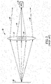
Figure 1 shows a schematic sectional view of alaser scanner 10 described inU.S. Pat. Pub. No. 2013/0003041 . In operation, alight source 12, such as a laser diode, emits a collimatedbeam 14 in the form of short (e.g., few nanoseconds) pulses toward a bending or foldingmirror 16, which reflects the beam toward a scanningmirror 18, which directs the beam toward ascanning area 20. If an object is present in thescanning area 20, thediffuse light 22 that is back-reflected by the object is reflected by thescanning mirror 18, collected by acollecting lens 24 and detected by a light detector 26 (e.g., a photodiode). A similar laser scanner is disclosed inUS5202784 . - A
motor 28 may be operatively coupled to thescanning mirror 18 to drive the scanning mirror in continuous rotation about a vertical axis of rotation. The angular position of thescanning mirror 18 may be detected by anangular position detector 30, such as an encoder. Thelight beam 14 generated by thelight source 12 therefore scans thescanning area 20 generated by the rotational movement. In instances where there is an object in thescanning area 20 and a reflected light signal is detected by thelight detector 26, the angular position of the object in the scanning area may be derived from the angular position of thescanning mirror 18, as detected by theangular position detector 30. - The time of flight of individual laser light pulses from their transmission until the reception after reflection by the object in the
scanning area 20 may be determined, which allows for calculation of the distance of the object from thelaser scanner 10 based on the known speed of light. This evaluation may be performed by acontroller 32 which is operatively coupled to thelight source 12, thelight detector 26, themotor 28, and/or theangular position detector 30. - The components of the
laser scanner 10 may be arranged in ahousing 34 which includes aprotective window 36 in the area where light enters and leaves the laser scanner. - As shown in
Figure 1 , thetransmission path 38 and thereception path 22 are coaxial, which avoids a parallax offset at short distances. However, the transmission optical elements (e.g., bending mirror 16) provide a central obstruction in the reception path. Thus, for light reflected back from objects at a relatively far distance, theincoming beam 22 fills the sensitive area of thelight detector 26 and the central obstruction causes a flux loss (e.g., 10 % flux loss). For objects at a relatively short distance, however, the incoming beam on the plane of thelight detector 26 will be defocused and the shadow of the central obstruction will be enlarged. Such shadow causes a strong reduction of the signal for objects near thelaser scanner 10, which could cause the laser scanner to fail to detect objects at short ranges (e.g., less than 1 meter). - As shown in
Figure 2 , to overcome this problem, acollecting lens 40 may be provided that is divided into two more sections or concentric rings, such as amarginal section 42 and acentral section 44. For anobject 46 which is relatively close to the laser scanner, themarginal rays 48 will not hit thelight detector 26 and thus will not contribute to the measured signal. Thecentral section 44 of thelens 40 has a shorter focal distance and will bend therays 50 coming from the near range toward thelight detector 26 to be detected thereby. -
Figure 3 shows a portion of anoptical system 60 for a laser scanner which includes a light source 62 (e.g., laser diode) which directs a collimatedbeam 64 toward afolding mirror 66 which directs the beam to ascanning area 68.Input light 70 reflected from objects in thescanning area 68 may be collected by acollecting lens 72, which focuses the light onto a light detector 74 (e.g., photodiode). Aninterference filter 76 may be positioned on top of (as shown) thelight detector 74 to block light which is outside the wavelength band of the light source. The optical path length (OPL) is also shown inFigure 2 . - The
interference filter 76 may have a transmission efficiency which is dependent on the incidence angle A1. In some instances, due to the working f-number of the collecting lens being close to 1, theinterference filter 76 typically must acceptrays 78 with an incidence angle of up to 30 degrees. With such a relatively wide acceptance angle for theinterference filter 76, the interference filter may be required to pass not only the rays from the reception path but also light which is scattered by unwanted reflections inside the housing of the laser scanner. - A laser scanner to detect objects in a scanning area may be summarized as including: a transmission subsystem and a reception subsystem, the transmission subsystem including: a light source which in operation emits a light beam; and a scanning mirror rotatable about an axis of rotation which reflects the light beam from the light source toward the scanning area and which directs return light from objects in the scanning area toward the reception subsystem; the reception subsystem, including: a collecting mirror dimensioned and positioned to receive the return light from the scanning mirror; an interference filter disposed between the collecting mirror and the scanning mirror, in operation the interference filter filters the return light from the scanning mirror and provides the filtered return light to the collecting mirror; and a light detector disposed between the interference filter and the collecting mirror, in operation the light detector receives the filtered return light reflected from the collecting mirror.
- The collecting mirror may have a reflective surface which has an aspheric profile. The collecting mirror may have a reflective surface which is defined at least in part by an N degree polynomial, where N is an integer greater than or equal to three. The collecting mirror may have a reflective surface which is defined at least in part by a Zernike polynomial or a Chebyshev polynomial. The collecting mirror may have a reflective surface which has a continuous curvature. The collecting mirror may have a reflective surface which comprises at least one layer of a reflective coating disposed over a plastic material. The reflective coating of the collecting mirror may include at least one of an aluminum coating, a silver coating, or a gold coating, and the plastic material comprises at least one of polycarbonate (PC), polymethylmethacrylate (PMMA), or cyclic olefin polymer (COP). The plastic material may be absorptive to the light beam emitted by the light source. The light source may include a laser diode, and the light detector may include an avalanche photodiode. The interference filter may include a bandpass filter which filters light having wavelengths which are outside a spectrum of the light beam emitted by the light source. The interference filter may include a colored glass substrate.
- The laser scanner may further include a first folding mirror disposed in an optical path between the light source and the scanning mirror.
- The first folding mirror may have a reflective surface which is parallel with a reflective surface of the scanning mirror. The first folding mirror may have a reflective surface which is non-parallel with a reflective surface of the scanning mirror. The first folding mirror may reflect the light beam at an angle of reflection other than 45 degrees with respect to normal. The laser scanner may further include a second folding mirror disposed in the optical path between the light source and the first folding mirror.
- The first folding mirror and the second folding mirror may have respective reflective surfaces which are parallel to each other. At least one of the first folding mirror and the second folding mirror may have a reflective surface which is non-parallel with a reflective surface of the scanning mirror. At least one of the first folding mirror and the second folding mirror may reflect the light beam at an angle of reflection other than 45 degrees with respect to normal. The collecting mirror may include a compound mirror comprising a central mirror which has a reflective surface which has a parabolic profile or an elliptical profile, and an outer ring mirror which surrounds the central mirror, the outer ring mirror having a reflective surface which has an aspheric profile. An outer edge of the reflective surface of the central mirror may have a first tangent value, and an inner edge of the reflective surface of the outer ring mirror may have a second tangent value, the second tangent value equal to the first tangent value to provide continuous curvature between the reflective surface of the central mirror and the reflective surface of the outer ring mirror. The reflective surface of the outer ring mirror may be defined at least in part by an N degree polynomial, where N is an integer greater than or equal to three. The reflective surface of the outer ring mirror may be defined at least in part by a Zernike polynomial or a Chebyshev polynomial.
- A method of operating a laser scanner is recited in
claim 10. - Reflecting, by a collecting mirror, the filtered return light toward a light detector may include reflecting by a collecting mirror which has a reflective surface having an aspheric profile. Reflecting, by a collecting mirror, the filtered return light toward a light detector may include reflecting by a collecting mirror which has a reflective surface defined at least in part by a Zernike polynomial, a Chebyshev polynomial, or an N degree polynomial, where N is an integer greater than or equal to three.
- The method of operating a laser scanner to detect objects in a scanning area may further include folding, by a first folding mirror disposed in an optical path between the light source and the scanning mirror, the light beam between the light source and the scanning mirror. Folding the light beam between the light source and the scanning mirror may include folding the light beam by a first folding mirror which has a reflective surface which is parallel with a reflective surface of the scanning mirror. Folding the light beam between the light source and the scanning mirror may include folding the light beam by a first folding mirror which has a reflective surface which is non-parallel with a reflective surface of the scanning mirror. Folding the light beam between the light source and the scanning mirror may include folding the light beam by the first folding mirror by an angle of reflection which is less than 45 degrees.
- The method of operating a laser scanner to detect objects in a scanning area may further include folding, by a second folding mirror disposed in the optical path between the light source and the first folding mirror, the light beam between the light source and the first folding mirror.
- Folding the light beam between the light source and the scanning mirror by the first folding mirror and the second folding mirror may include at least one of: folding the light beam by the first folding mirror by an angle of reflection which is less than 45 degrees, and folding the light beam by the second folding mirror by an angle of reflection which is less than 45 degrees. Folding the light beam between the light source and the scanning mirror by the first folding mirror and the second folding mirror may include folding the light beam by the first folding mirror by an angle of reflection which is less than 45 degrees and folding the light beam by the second folding mirror by an angle of reflection which is less than 45 degrees. Reflecting, by a collecting mirror, the filtered return light toward a light detector may include reflecting by a collecting mirror which comprises a compound mirror including a central mirror which has a reflective surface which has a parabolic profile or an elliptical profile, and an outer ring mirror which surrounds the central mirror, the outer ring mirror having a reflective surface which has an aspheric profile. Reflecting, by a collecting mirror, the filtered return light toward a light detector may include reflecting by the compound mirror, and an outer edge of the reflective surface of the central mirror may have a first tangent value, and an inner edge of the reflective surface of the outer ring mirror may have a second tangent value, the second tangent value equal to the first tangent value to provide continuous curvature between the reflective surface of the central mirror and the reflective surface of the outer ring mirror. Reflecting, by a collecting mirror, the filtered return light toward a light detector may include reflecting by the compound mirror, and the reflective surface of the outer ring mirror may be defined at least in part by an N degree polynomial, where N is an integer greater than or equal to three. Reflecting, by a collecting mirror, the filtered return light toward a light detector may include reflecting by the compound mirror, and the reflective surface of the outer ring mirror may be defined at least in part by a Zernike polynomial or a Chebyshev polynomial.
- An optical system for a laser scanner which detects objects in a scanning area may be summarized as including: a light source which in operation emits a laser beam; a scanning mirror rotatable about an axis of rotation which reflects the laser beam from the light source toward the scanning area and which reflects return light from objects in the scanning area; a collecting mirror dimensioned and positioned to receive the return light from the scanning mirror; an interference filter disposed between the collecting mirror and the scanning mirror; and a light detector disposed between the interference filter and the collecting mirror.
- In the drawings, identical reference numbers identify similar elements or acts. The sizes and relative positions of elements in the drawings are not necessarily drawn to scale. For example, the shapes of various elements and angles are not necessarily drawn to scale, and some of these elements may be arbitrarily enlarged and positioned to improve drawing legibility. Further, the particular shapes of the elements as drawn, are not necessarily intended to convey any information regarding the actual shape of the particular elements, and may have been solely selected for ease of recognition in the drawings.
-
Figure 1 is a schematic sectional view of a laser scanner. -
Figure 2 is a schematic diagram of a sectioned lens for a laser scanner. -
Figure 3 is a schematic sectional view of a portion of an optical system for a laser scanner, such as the laser scanner ofFigure 1 . -
Figure 4A is a schematic sectional view of a laser scanner showing a transmission period of the laser scanner, according to one illustrated implementation. -
Figure 4B is a schematic sectional view of the laser scanner ofFigure 4A showing a reception period of the laser scanner, according to one illustrated implementation. -
Figure 5 is a schematic sectional view of a portion of an optical system for the laser scanner ofFigure 4A , according to one illustrated implementation. -
Figure 6 is a schematic diagram showing the shape of a clear aperture of a reception subsystem for a laser scanner, according to one illustrated implementation. -
Figure 7A is a schematic diagram showing a focused image relative to a sensitive area of a light detector at a far-range distance, according to one illustrated implementation. -
Figure 7B is a schematic diagram showing a defocused image relative to a sensitive area of a light detector at a mid-rangedistance, according to one illustrated implementation. -
Figure 7C is a schematic diagram showing a defocused image relative to a sensitive area of a light detector at a near-range distance, according to one illustrated implementation. -
Figure 8 is a graphical plot of signal power as a function of distance for a sectioned lens, a parabolic reflector and an aspheric reflector, according to one illustrated implementation. -
Figure 9A is a schematic sectional view of a transmission subsystem of a laser scanner which includes a laser source aimed vertically upwards and two folding mirrors, according to one illustrated implementation. -
Figure 9B is a schematic sectional view of a transmission subsystem of a laser scanner which includes a laser: source aimed vertically downward and two folding mirrors, according to one illustrated implementation. -
Figure 9C is a schematic sectional view of a transmission subsystem of a laser scanner which includes a folding mirror tilted at an angle different from 45 degrees, according to one illustrated implementation. -
Figure 9D is a schematic sectional view of a transmission subsystem of a laser scanner which includes two folding mirrors each tilted at angles different from 45 degrees, according to one illustrated implementation. -
Figure 10A is an elevational view of a compound collecting mirror, according to one illustrated implementation. -
Figure 10B is a top plan view of the compound collecting mirror ofFigure 10A , according to one illustrated implementation. -
Figure 11 is a schematic sectional view of a reception subsystem of a laser scanner which includes a compound collecting mirror, showing light returned from a distant object, according to one illustrated implementation. -
Figure 12 is a schematic sectional view of a reception subsystem of a laser scanner which includes a compound collecting mirror, showing light returned from a near object, according to one illustrated implementation. -
Figure 13 is a schematic sectional view of a reception subsystem of a laser scanner which includes a compound collecting mirror, showing a tailored profile of an outer ring mirror of the compound collecting mirror which covers a short range by associating each point on the outer ring mirror to a determined object distance, according to one illustrated implementation. -
Figure 14 is a schematic sectional view of a reception subsystem of a laser scanner which includes a compound collecting mirror, showing a detailed view of a cut-off range for objects which are very close to a protective window of the laser scanner, according to one illustrated implementation. -
Figure 15 is a graphical plot of signal power as a function of distance for a parabolic reflector, an aspheric reflector, and a compound reflector, according to one illustrated implementation. -
Figure 16 is a schematic sectional view of a compound collecting mirror which comprises a central mirror and an outer ring mirror, showing a continuous curvature between an outer edge of the central mirror and an inner edge of the outer ring mirror, according to one illustrated implementation. - In the following description, certain specific details are set forth in order to provide a thorough understanding of various disclosed implementations. However, one skilled in the relevant art will recognize that implementations may be practiced without one or more of these specific details, or with other methods, components, materials, etc.
- Unless the context requires otherwise, throughout the specification and claims that follow, the word "comprising" is synonymous with "including," and is inclusive or open-ended (i.e., does not exclude additional, unrecited elements or method acts).
- Reference throughout this specification to "one implementation" or "an implementation" means that a particular feature, structure or characteristic described in connection with the implementation is included in at least one implementation. Thus, the appearances of the phrases "in one implementation" or "in an implementation" in various places throughout this specification are not necessarily all referring to the same implementation. Furthermore, the particular features, structures, or characteristics may be combined in any suitable manner in one or more implementations.
- As used in this specification and the appended claims, the singular forms "a," "an," and "the" include plural referents unless the context clearly dictates otherwise. It should also be noted that the term "or" is generally employed in its sense including "and/or" unless the context clearly dictates otherwise.
- The headings and Abstract of the Disclosure provided herein are for convenience only and do not interpret the scope or meaning of the implementations.
- One or more implementations of the present disclosure are directed to laser scanners and optical systems for laser scanners which may be used in any number of applications, such as safety applications. The optical system of one or more implementations may include an emitting or transmission subsystem which scans a scanning area using a laser beam. The optical system may also include a reception subsystem which detects light (visible or nonvisible, more generally "electromagnetic radiation") scattered back by an object positioned inside the scanning area. Compared to existing systems and methods, one or more of the implementations discussed herein provide relatively better performance and/or allow for relatively reduced dimensions.
- Referring to
Figures 4A, 4B and5 , alaser scanner 100 is shown, according to one illustrated implementation. As shown inFigure 4A , thelaser scanner 100 includes a light source oremitter 102, such as a laser diode, that emits a collimatedbeam 104 in the form of short (e.g., few nanoseconds) pulses toward a bending orfolding mirror 106, which reflects the beam toward ascanning mirror 108. Thelight source 102 may have an emission band in the near infrared (NTR) range and may have a peak wavelength of 905 nanometers, for example. Thescanning mirror 108 directs the beam toward ascanning area 110. - As shown in
Figure 4B , if an object is present in thescanning area 110, diffuse light 112 that is back-reflected by the object is reflected by thescanning mirror 108, and directed downward toward collecting optics which include a concave collecting reflector ormirror 114. The collectingmirror 114 is positioned below thefolding mirror 106 to direct and focus light from thescanning mirror 108 which has been reflected from one or more objects positioned within thescanning area 110 toward a light detector 116 (e.g., avalanche photodiode, other photodetector) which is supported by asupport arm 118. - The collecting
mirror 114 may be formed of a plastic material (e.g., polycarbonate (PC), polymethylmethacrylate (PMMA), cyclic olefin polymer (COP)) which has a one or more layers of a reflective coating thereon to provide a reflective surface 115 (Figure 5 ). The reflective coating may include a metal layer such as aluminum or gold, optionally with a protective layer of a transparent material (e.g., SiO2). Another example of a reflective coating is a dielectric multilayer coating that has a very high (e.g., 99%)reflectivity for a specific wavelength band. The collectingmirror 114 may be formed from a material with low water absorption properties which may reduce the likelihood that a reflective coating will peel off during the lifetime of thelaser scanner 100. In some implementations, the collectingmirror 114 is opaque to wavelengths of light emitted by thelight source 102 so that the small fraction of light which passes through thereflective surface 115 is absorbed by the material and is not diffused inside ahousing 122 of thelaser scanner 100. - The
laser scanner 100 also includes a dichroic orinterference filter 120 positioned above (as shown) thelight detector 116 to filter the returned light 112 from thescanning mirror 108 before the returned light reaches the collectingmirror 114. Theinterference filter 120 transmits spectral bands which correspond to the light emitted by thelight source 102 and reflects spectral bands outside of the spectral band emitted by the light source. Since theinterference filter 120 is placed in the optical path before the collectingmirror 114, the interference filter may be designed to accept rays with an relatively small incidence angle A2 (Figure 5 ), such as an incidence angle of only a few degrees (e.g., 3 degrees, 5 degrees, 10 degrees, 20 degrees). By allowing the acceptance angle of theinterference filter 120 to be relatively small, the interference filter may more effectively filter the scattered light from within thehousing 122 of thelaser scanner 100, thereby improving the signal to noise ratio. - In some implementations, the
interference filter 120 is made with a colored class filter substrate having a single or multilayer coating on one or both sides thereof. The glass material may be, for example, Schott RG830 glass offered by Schott Corporation or Hoya IR-83 glass offered by Hoya Corporation. Theinterference filter 120 may in some implementations have a black appearance because the glass material may not be transparent to visible light but has a relatively high transmittance (e.g., greater than 90%) in the NIR region emitted by thelight source 102. Additional layer(s) may be operative to filter wavelengths of light beyond the emission band of thelight source 102. The collectingmirror 114 andinterference filter 120 are discussed in further detail below. - The
laser scanner 100 may also include a motor/detector 124 which is operatively coupled to thescanning mirror 108 to drive the scanning mirror in continuous rotation about a vertical axis of rotation. For example, in some implementations thescanning mirror 108 may rotate at an approximate speed of 2000 rotations per minute. The angular position of thescanning mirror 108 may be detected by the motor/detector 124, which may include an angular position detector such as an encoder. Thelight beam 104 generated by thelight source 102 in the form of short pulses therefore scans thescanning area 110 generated by the rotational movement. In instances where there is an object in thescanning area 110 and a reflected light signal is detected by thelight detector 116, the angular position of the object in thescanning area 110 may be derived from the angular position of thescanning mirror 108, as detected by the motor/detector 124. - The time of flight of individual laser light pulses from their transmission until the reception after reflection on the object in the
scanning area 110 may be determined, which allows for calculation of the distance of the object from thelaser scanner 100 based on the known speed of light. This evaluation may be performed by acontroller 126 which is operatively coupled to thelight source 102, thelight detector 116, and/or the motor/detector 124. - The
controller 126 may be any suitable controller, and may include one or more central processing units (CPUs), microprocessors, digital signal processors (DSPs), application-specific integrated circuits (ASICs), field programmable gate arrays (FPGAs), programmable logic controllers (PLCs), etc. Thecontroller 126 may include or be operatively coupled to nontransitory processor-readable storage media (e.g., RAM, ROM, flash), input/output systems, wired/wireless communication systems, etc., as is known in the art. - The components of the
laser scanner 100 may be arranged in thehousing 122 which includes aprotective window 128 in the area where light enters and leaves the laser scanner. Theprotective window 128 may be made of a plastic material (e.g., polycarbonate, other polymer material) which has a high transmittance of light for wavelengths which are emitted by thelight source 102. In some implementations, the visual appearance of thewindow 128 may be black, which filters visible light and which hides the internal components of thelaser scanner 100. Thewindow 128 may have rotation symmetry about the vertical axis of rotation of thescanning mirror 108. - In some implementations, the
protective window 128 has a profile which is divided into anupper section 128A, amiddle section 128B, and alower section 128C. Themiddle section 128B of theprotective window 128 may be tilted with a relatively large angle (e.g., 30 degrees, 45 degrees) with respect to the vertical axis, which provides at least two benefits. First, for at least some coating processes the inner and outer surface of thewindow 128 can be effectively coated with an anti-reflective coating only if the tilt of the window is above a certain angle (e.g., more than 30 degrees). This is because the dielectric material in the vacuum deposition process comes from a direction which is parallel to the vertical symmetry axis and cannot substantially stack on vertical or nearly vertical surfaces. Second, by providing the tiltedmiddle section 128B of theprotective window 128; the small fraction of light transmitted from thelight source 102 which undergoes specular reflection is directed downward away from the optical path of the receiving subsystem and can be stopped by a light absorbing material positioned within thehousing 122 of thelaser scanner 100. - By utilizing the collecting
reflector 114 rather than a lens for the concentrator optics, several limitations of conventional collecting lenses may be mitigated. For example, the large numerical aperture requirements typically result in a relatively thick lens with a short radius of curvature. In such instances, the irradiance distribution spot at the focus point of the lens may be strongly affected by inhomogeneities in the lens material. Such is an issue when the lens is made of glass, and may be worse in cases where the lens is made from a plastic material. Additionally, due to the relatively large thickness of the lens, the birefringence of the lens material may introduce aberrations in the spot image at the focal plane of the lens. The thickness of the lens also increases the length of the optical system, which results in a larger housing requirement for the laser scanner. As shown inFigure 5 , the optical path length (OPL) of the optical system of thelaser scanner 100 may be substantially shorter than the OPL of a system which utilizes a thick lens (secFigure 3 ). Further, the index of refraction of a lens is temperature dependent and, in combination with the thermal expansion of the lens material, the focus position of the lens will shift due to variations in temperature. - Utilizing the
reflector 114 as the collecting optics for thelaser scanner 100 rather than a thick lens has further advantages. For example, thereflector 114 may have a relatively thin profile compared to a lens, due to the smaller thickness and larger radius of curvature of the reflector. Additionally, shapes having a larger radius of curvature are easier to mold with a given precision. Additionally, by using a reflector, the focus configuration is independent of the refractive index of the material which, as noted above, may change due to changes in environmental conditions. Further, when using a reflector the quality of the spot on the plane of thelight detector 116 is not affected by material inhomogeneities, internal stresses, bubbles and birefringence. Moreover, a reflector may be made of only one optical surface and the mold for the reflector may only require one optical mold insert, compared to two optical mold inserts required for using a lens for the collecting optics. - Additionally, in some instances, a reflector with a reflective coating (e.g., aluminum coating, silver coating, gold coating) may have a higher flux transfer efficiency than a lens, even when the lens has an anti-reflective coating on both sides thereof. Advantageously, during manufacturing a reflective surface may be coated with a layer of material by a single coating process, whereas an effective anti-reflective coating on a lens may require multiple coating processes (e.g., application of multiple coating layers on one or both sides of a lens).
-
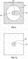
Figure 6 is a schematic diagram showing the shape of aclear aperture 140 of a reception subsystem for thelaser scanner 100, As shown, theclear aperture 140 is "C" shaped due to acentral obstruction 142 caused by thelight detector 116 and itssupport arm 118. InFigure 6 the portion of thecentral obstruction 142 caused by thelight detector 116 is identified byreference numeral 144 and the portion of the central obstruction caused by thesupport arm 118 is identified byreference numeral 146. -
Figure 7A is a schematic diagram showing a focused spot orimage 150 relative to asensitive area 152 of thelight detector 116 at a relatively far-range distance. As shown, when an object is at a relatively far distance, the entrance profile pupil is not visible because the rays which make up thefocused image 150 are focused on thesensitive area 152 of thelight detector 116. - As shown in
Figure 7B , when an object is at a mid-range distance, animage 154 is slightly defocused, which causes some of the image to appear outside of thesensitive area 152 of thelight detector 116. As shown inFigure 7C , when an object is closer than a minimum distance, adefocused image 156 is larger and surrounds thesensitive area 152 of thelight detector 116, causing substantially no signal to be detected by the light detector. In the condition shown inFigure 7C , thelight detector 116 is "blind" and cannot detect objects which are closer than the minimum distance to thelaser scanner 100. - If the collecting mirror has the shape of a simple parabolic profile, the blind zone shown in
Figure 7C for objects at short distances can extend out as far as 1 meter or more which, in many applications, may be unacceptable. For instance, in some applications, it may be desirable to detect objects at relatively short distances (e.g., 20 cm, 10 cm, 5 cm). - A fine-tuning of the "cut-off" detection distance may be implemented to set a balance between two opposing requirements: objects positioned at short distances should be detected, but the scattered light from the
protective window 128 should not disturb the object detection. Even if theprotective window 128 has clean and polished surfaces, a small amount of back scattering and the associated flux may be comparable or even higher than the signal from an object that is close to the device and has a low reflectance surface. Under such a condition, the object signal is blended with the scattered light from theprotective window 128 and no detection may occur. Further, in practical application environments, dust particles and/or droplets may gather on the outer surface of theprotective window 128, which increases the fraction of scattered light and potentially increases this problem. - To overcome these and other issues, in some implementations the collecting
reflector 114 may have an aspheric surface profile which can successfully modulate the width and position of the blind zone shown inFigure 7C . Such an aspheric profile may be described by a polynomial function having a degree N, where N is an integer greater than or equal to three, for example. As another example, the aspheric profile may be described by a Zernike polynomial or a Chebyshev polynomial. The cut-off distance is sensitive to profile of the collecting reflector and to the position and diameter of the obstruction. - The aspheric profile of the collecting
mirror 114 compresses a signal power function to extend the detection range of a laser scanner to relatively short distances and to block backscattered light from theprotection window 128 of thelaser scanner 100. In contrast to a sectioned lens (Figure 2 ), the aspheric profile of the collectingmirror 114 may have a smooth profile with no curvature discontinuity, for example. The particular profile of the collecting reflector may be designed to cover the blind zone while providing a smooth plot of signal power as a function of distance. -
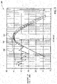
Figure 8 shows an examplegraphical plot 160 of signal power as a function of distance for a sectionedlens 162, aparabolic reflector 164 and anaspheric reflector 166. As can be seen from the plot, the signal power for a parabolic reflector 164 (i.e., collecting optics without near field coverage correction) drops significantly at short distances due to the blind zone discussed above. In the case of a sectioned lens 162 (seeFigure 2 ), the signal power shows an undesirable ripple in the near field due to the discontinuity in the lens profile. Conversely, the signal power for theaspheric reflector 166 is continuous without the ripple and maintains a relatively high signal power at short distances. - A non-limiting example equation for the surface profile of the collecting
reflector 114 is a third degree polynomial defined by:
- The r2 term defines a parabola with its focusing properties. The r term and the r3 term introduce a deviation which produces a more flat power function, as shown in
Figure 8 . Although a third degree polynomial is shown above as an example, depending on the system geometry for a particular application it may be desirable to define the surface profile of the collecting reflector with a polynomial of a higher degree (e.g., 4th degree, 6th degree). -
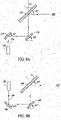
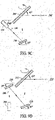
Figures 9A-9D show additional arrangements for the transmission path of a laser beam in a laser scanner, such as thelaser scanner 100 ofFigures 4A-4B discussed above, which may be used to provide a more compact design and/or to provide other benefits (e.g., beam alignment). - In
Figure 9A , alaser source 170 is aimed vertically upward (as shown) toward afirst bending mirror 172 which is tilted upward (from left to right) at a 45 degree angle. Thefirst bending mirror 172 reflects alaser beam 174 emitted by thelaser source 170 horizontally (as shown) at a right angle toward asecond bending mirror 176 tilted upward at a 45 degree angle. Thesecond bending mirror 176 reflects thelaser beam 174 vertically upward at a right angle toward arotating scanning mirror 178, which reflects thelaser beam 174 horizontally toward ascanning area 180. - In
Figure 9B , alaser source 182 is aimed vertically downward toward afirst bending mirror 184 which is tilted downward (from left to right) at a 45 degree angle. The first bending mirror reflects alaser beam 186 emitted by thelaser source 182 horizontally (as shown) at a right angle toward a second bending mirror 188 tilted upward at a 45 degree angle. The second bending mirror 188 reflects thelaser beam 186 vertically upward at a right angle toward arotating scanning mirror 190, which reflects the laser beam horizontally toward ascanning area 192. - By utilizing two bending mirrors as shown in
Figures 9A and 9B , the laser source of a laser scanner may be aimed in a vertical direction which in some applications may allow for a more compact design and/or may provide desirable beam alignment advantages. - In
Figure 9C , alaser source 194 is aimed downward at an angle of approximately 40 degrees from horizontal toward abending mirror 196 which is tilted upward at an angle of approximately 25 degrees. Thebending mirror 196 reflects alaser beam 198 emitted by thelaser source 194 vertically upward toward arotating scanning mirror 200, which reflects thelaser beam 198 horizontally toward a scanning area202. - In
Figure 9D , alaser source 204 is aimed vertically upward toward afirst bending mirror 206 which is tilted upward at an angle of approximately 20 degrees. Thefirst bending mirror 206 reflects alaser beam 208 emitted by thelaser source 204 downward toward asecond bending mirror 210 tilted upward at an angle of approximately 20 degrees. Thesecond bending mirror 210 reflects thelaser beam 208 vertically upward toward arotating scanning mirror 212, which reflects thelaser beam 208 horizontally toward ascanning area 214. - As shown in
Figures 9C and 9D , the tilt angle of the bending mirrors may be other than 45 degrees (e.g., 15 degrees, 30 degrees, 60 degrees) and in instances where more than one bending mirror (e.g., two, three) is used, the optical path may be more compact that instances where one or more bending mirrors are each tilted at 45 degrees. - The collecting mirror profiles discussed above achieve the goal of compressing the dynamic extension of the signal throughout the measurement range and covering short distances when the central obstruction of the bending mirror is generally less than 1/4 of the full diameter of the entrance pupil diameter (EPD) of the receiving optics. When the range extends further (e.g., 7-8 meters) and the central obstruction is larger, it may not be possible to match the efficiency at such a long range while providing coverage at the short range (e.g., a few centimeters). For instance, it has been found that when the central obstruction approaches 1/3 of the entrance pupil diameter (EPD), it may be desirable or necessary to focus most or all of the entrance beam which is captured by the scanning mirror and not obstructed by the central obstruction on the sensitive area of the detector to obtain the maximum efficiency.
-
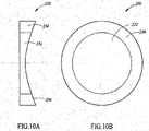
Figures 10A and 10B show an implementation of acompound collection mirror 250 which includes two concentric areas comprising aninner mirror 252 having atop surface 253 which is used to focus incoming light to detect long range objects and anouter ring mirror 254 which is used to focus incoming light to detect short range objects. Thetop surface 253 of theinner mirror 252 may have a parabolic profile, an elliptical profile or other suitable profile (e.g., aspheric). For example, thetop surface 253 of theinner mirror 252 may have a profile of an elongated ellipse, with a first (near) focus at the detector and a second (far) focus at a maximum ranging distance (e.g., 5 meters, 10 meters). Atop surface 256 of theouter ring mirror 254 may have a curvature which is tailored to cover the short range with a substantially constant efficiency in the short distance and a rapid drop in efficiency for objects which are very near the protective window of the scanner and for light reflected from the protective window itself. - As shown in
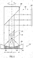
Figure 11 , when anobject 260 is far away (e.g., 5-8 meters) from the scanner, reflectedrays 262 are substantially parallel and the diameter (D1) of the illuminated area on the collectingmirror 250 is the same as or just slightly larger than the EPD determined by the dimensions of thescanning mirror 108. - When the
object 260 gets closer, as shown inFigure 12 , a reflectedbeam 264 becomes diverging from the spot projection on the target plane and the illuminated area of the collecting mirror surfaces has a diameter (D2) which extends to theouter ring mirror 254. As the distance of theobject 260 is reduced relative to the scanner, a larger area is illuminated by the incoming radiation. If the focal distance associated with thering mirror 254 is shorter than the focal distance of the inner orcentral mirror 252, thedetector 116 can see objects which are close to the scanner. As discussed below, a tailored design procedure can set a cut off distance so that a reflective signal from the protective window surface is nulled or minimized to cause little or no disturbance to the detection of objects in the scanning field. - Further, it may be desirable to compress the dynamic range of the detection signal as much as possible. Generally, the receiving optics should be designed to have the maximum efficiency at long distances, limited peak of efficiency in the intermediate range, and provide signal coverage at very short distances (e.g., a few centimeters).
- As shown in
Figure 13 , when an object is close to the scanner, the outer area of the collectingmirror 250 is illuminated by the reflected radiation and it is possible to deflect rays toward thedetector 116 by increasing the slope of thetop surface 256 of thering mirror 254. It is noted that thetop surface 253 of thecentral mirror 252 may be parabolic or elliptical to maintain maximum efficiency for long ranges (e.g., 2 or more meters). Thus, theouter ring mirror 254 may work in the medium and short ranges only (e.g., 0-2 meters). - As shown in
Figure 13 , reflected light 274 from an object at a relatively close distance 270 (e.g., a few centimeters) hits thetop surface 256 of thering mirror 252 at anouter edge 272 thereof due to the larger diameter of the reflected light. Reflected light 282 from an object at a relatively further distance (e.g., 1-2 meters) hits thetop surface 256 of thering mirror 252 at apoint 280 inward of theouter edge 272 of thering mirror 252 due to the relatively smaller diameter of the reflected light. As noted above, reflected light from an object at a relatively long range (e.g., greater than 2 meters) hits only thecentral mirror 252 due to the relatively smaller diameter (e.g., diameter D1 ofFigure 11 ) of the reflected light. It is noted that therays - Thus, as an object gets closer to the scanner, a gradually larger diameter of the collecting
mirror 250 is hit by the reflected light. In some implementations, the profile for thetop surface 256 of thering mirror 256 may be calculated using a process known in technical literature on non-imaging optics to match incoming rays angles with reflected rays so that the rays can hit thedetector 116. See, for example, W. Elmer, The Optical Design of Reflectors, Wiley, 1980, and J. Chaves, Introduction to Nonimaging optics, CRC Press, 2008. In some implementations, the profile for thetop surface 256 of thering mirror 254 may be calculated at discrete points that match incident and reflected ray angles, and then transformed into a smooth profile via interpolation with a polynomial (e.g., 3rd degree polynomial, 4th degree polynomial, etc.). As another example, the profile of thetop surface 256 of theouter ring mirror 254 may be described by a Zernike polynomial, a Chebyshev polynomial, or other suitable expression. -
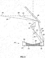
Figure 14 shows a detailed view of a cut-off range for objects that are very close to the protective window of the scanner. As discussed above with reference toFigure 13 ,rays 274 coming from an object at thedistance 270 hit theouter edge 272 of thering mirror 254 and are focused on thedetector 116.Rays 282 coming from an object at thedistance 278 hit thepoint 282 inward of theouter edge 272 and are focused on thedetector 116.Rays close distance 286 either miss the collectingmirror 250 altogether (ray 290) or are reflected by thering mirror 254 but miss the detector 116 (ray 288). Thus, the scanner will not detect objects which are very close to the protective window of the scanner, including the protective window itself. - Utilizing this design, it is possible to move the "knee" of the signal power function where the signal power changes its shape from nearly flat to the inverse square law. As can be seen in
Figure 14 , theedge ray 274 that hits thering mirror 254 at theshortest distance 270 in the cut-off range still hits thedetector 116, but rays 288 and 290 which are reflected from an object at theshorter distance 286 will miss thedetector 116 and/or the collectingmirror 250. - The tuning of this geometry allows the designer to set the cut-off distance and, due to a large angle α (see
Figure 13 ), the transition from a high signal to a very low or no signal may be reduced to a span of a few centimeters. The precise positioning of the cut-off distance may be tuned in a calibration stage of the manufacturing process so that the scanner receives a faint signal from light reflected by the protective window but a strong enough signal from an object just a few centimeters outside the protective window. -
Figure 15 shows a plot 300 of signal power as a function of object distance for aparabolic mirror 302, an aspheric mirror 304 (e.g., mirror 114), and a compound mirror 306 (e.g., compound mirror 250). As shown, thecompound mirror 306 has a relatively flat profile which drops off sharply at a "knee" 308. Thus, thecompound mirror 306 covers a blind zone at short distances while cutting off signals from the protective window or signals from objects very near the protective window. -
Figure 16 shows a detailed view of the curvature profile for thetop surface 253 of theinner mirror 252 and thetop surface 256 of theouter ring mirror 254 of thecompound mirror 250. A theoreticalparabolic surface 310 is shown below thetop surface 256 for reference to show the greater curvature of thetop surface 256 compared to a parabolic surface. The curvatures shown inFigure 16 are exaggerated for the purpose of illustration. At apoint 314 wherein thetop surface 253 of theinner mirror 252 joins thetop surface 256 of theouter ring mirror 254, atangent line 312 of thesurface 253 and thesurface 256 may be constrained to be the same. Such feature avoids a sudden deviation in the direction of rays that would otherwise cause a discontinuity in the signal power function at thepoint 314. - The implementations disclosed herein provide laser scanners which are compact, cost effective, less prone to molding tolerances, have higher optical efficiency, and provide a clear separation between the emission subsystem (e.g., upper part of the
housing 122 above the interference filter 120) and the receiving or reception subsystem (e.g., lower part of the housing below the interference filter). - The foregoing detailed description has set forth various implementations of the devices and/or processes via the use of block diagrams, schematics, and examples. Insofar as such block diagrams, schematics, and examples contain one or more functions and/or operations, it will be understood by those skilled in the art that each function and/or operation within such block diagrams, flowcharts, or examples can be implemented, individually and/or collectively, by a wide range of hardware, software, firmware, or virtually any combination thereof. Those of skill in the art will recognize that many of the methods or algorithms set out herein may employ additional acts, may omit some acts, and/or may execute acts in a different order than specified. The various implementations described above can be combined to provide further implementations.
- These and other changes can be made to the implementations in light of the above-detailed description. In general, in the following claims, the terms used should not be construed to limit the claims to the specific implementations disclosed in the specification and the claims, but should be construed to include all possible implementations along with the full scope of equivalents to which such claims are entitled. Accordingly, the claims are not limited by the disclosure.
Claims (15)
- A laser scanner (100) to detect objects in a scanning area (110), the laser scanner (100) comprising:a transmission subsystem and a reception subsystem, the transmission subsystem including:a light source (102) which in operation emits a light beam; anda scanning mirror (108) rotatable about an axis of rotation which reflects the light beam from the light source toward the scanning area (110) and which directs return light from objects in the scanning area (110) toward the reception subsystem;the reception subsystem, including:a collecting mirror (114) dimensioned and positioned to receive the return light from the scanning mirror (108);characterized by an interference filter (120) disposed between the collecting mirror (114) and the scanning mirror (108), in operation the interference filter (120) filters the return light from the scanning mirror (108) and provides the filtered return light to the collecting mirror (114); anda light detector (116) disposed between the interference filter (120) and the collecting mirror (114), in operation the light detector (116) receives the filtered return light reflected from the collecting mirror (114).
- The laser scanner (100) of claim 1 wherein the collecting mirror (114) has a reflective surface which has an aspheric profile or a continuous curvature, or which is defined at least in part by an N degree polynomial, where N is an integer greater than or equal to three, or by a Zernike polynomial or a Chebyshev polynomial.
- The laser scanner (100) of claim 1 wherein the light source (102) comprises a laser diode, and the light detector (116) comprises an avalanche photodiode.
- The laser scanner (100) of claim 1 wherein the interference filter (120) comprises at least one of a colored glass substrate or a bandpass filter which filters light having wavelengths which are outside a spectrum of the light beam emitted by the light source (102).
- The laser scanner (100) of claim 1, further comprising:
a first folding mirror disposed in an optical path between the light source (102) and the scanning mirror (108), wherein the first folding mirror reflects the light beam at an angle of reflection other than 45 degrees with respect to normal or has a reflective surface which is parallel with a reflective surface of the scanning mirror (108) or non-parallel with a reflective surface of the scanning mirror (108). - The laser scanner (100) of claim 5, further comprising:
a second folding mirror disposed in the optical path between the light source (102) and the first folding mirror, wherein the first folding mirror and the second folding mirror have respective reflective surfaces which are parallel to each other or non-parallel with a reflective surface of the scanning mirror (108), or wherein at least one of the first folding mirror and the second folding mirror reflect the light beam at an angle of reflection other than 45 degrees with respect to normal. - The laser scanner (100) of claim 1 wherein the collecting mirror (114) comprises a compound mirror comprising a central mirror which has a reflective surface which has a parabolic profile or an elliptical profile, and an outer ring mirror which surrounds the central mirror, the outer ring mirror having a reflective surface which has an aspheric profile.
- The laser scanner (100) of claim 7 wherein an outer edge of the reflective surface of the central mirror has a first tangent value, and an inner edge of the reflective surface of the outer ring mirror has a second tangent value, the second tangent value equal to the first tangent value to provide continuous curvature between the reflective surface of the central mirror and the reflective surface of the outer ring mirror.
- The laser scanner (100) of claim 7 wherein the reflective surface of the outer ring mirror is defined at least in part by an N degree polynomial, where N is an integer greater than or equal to three, or by a Zernike polynomial or a Chebyshev polynomial.
- A method of operating a laser scanner to detect objects in a scanning area (110), the method comprising:emitting, by a light source, a light beam;reflecting, by a scanning mirror (108) rotatable about an axis of rotation, the light beam emitted by the light source (102) toward the scanning area (110);characterized by reflecting, by the scanning mirror (108), return light reflected from objects in the scanning area (110) toward an interference filter (120) arranged between the scanning mirror (108) and a collecting mirror (114);filtering, by the interference filter (120), the return light from the scanning mirror (108) to provide filtered return light;reflecting, by the collecting mirror (114), the filtered return light toward a light detector (116) arranged between the interference filter (120) and the collecting mirror (114); anddetecting, by the light detector (116), the filtered return light reflected from the collecting mirror (114).
- The method of claim 10, further comprising:
folding, by a first folding mirror disposed in an optical path between the light source (102) and the scanning mirror (108), the light beam between the light source (102) and the scanning mirror (108). - The method of claim 11, further comprising:
folding, by a second folding mirror disposed in the optical path between the light source (102) and the first folding mirror, the light beam between the light source and the first folding mirror. - The method of claim 12 wherein folding the light beam between the light source (102) and the scanning mirror (108) by the first folding mirror and the second folding mirror comprises at least one of, or both of: folding the light beam by the first folding mirror by an angle of reflection which is less than 45 degrees, and folding the light beam by the second folding mirror by an angle of reflection which is less than 45 degrees.
- The method of claim 10 wherein reflecting, by a collecting mirror (114), the filtered return light toward a light detector (116) comprises reflecting by a collecting mirror (114) which comprises a compound mirror including a central mirror which has a reflective surface which has a parabolic profile or an elliptical profile, and an outer ring mirror which surrounds the central mirror, the outer ring mirror having a reflective surface which has an aspheric profile.
- The method of claim 14 wherein reflecting, by a collecting mirror (114), the filtered return light toward a light detector comprises reflecting by the compound mirror, and the reflective surface of the outer ring mirror is defined at least in part by an N degree polynomial, where N is an integer greater than or equal to three or by a Zernike polynomial or a Chebyshev polynomial.
Applications Claiming Priority (1)
| Application Number | Priority Date | Filing Date | Title |
|---|---|---|---|
| US15/145,532 US10048120B2 (en) | 2016-05-03 | 2016-05-03 | Laser scanner and optical system |
Publications (3)
| Publication Number | Publication Date |
|---|---|
| EP3246729A1 EP3246729A1 (en) | 2017-11-22 |
| EP3246729B1 EP3246729B1 (en) | 2019-04-24 |
| EP3246729B2 true EP3246729B2 (en) | 2022-08-24 |
Family
ID=58668799
Family Applications (1)
| Application Number | Title | Priority Date | Filing Date |
|---|---|---|---|
| EP17169257.7A Active EP3246729B2 (en) | 2016-05-03 | 2017-05-03 | Laser scanner and optical system |
Country Status (2)
| Country | Link |
|---|---|
| US (1) | US10048120B2 (en) |
| EP (1) | EP3246729B2 (en) |
Cited By (2)
| Publication number | Priority date | Publication date | Assignee | Title |
|---|---|---|---|---|
| DE102022129602A1 (en) | 2022-11-09 | 2024-05-16 | Ifm Electronic Gmbh | Cassegrain arrangement for an optical distance measuring system |
| DE102022129637A1 (en) | 2022-11-09 | 2024-05-16 | Ifm Electronic Gmbh | Optical scanner |
Families Citing this family (19)
| Publication number | Priority date | Publication date | Assignee | Title |
|---|---|---|---|---|
| US11585905B2 (en) | 2016-05-03 | 2023-02-21 | Datalogic Ip Tech S.R.L. | Laser scanner |
| US10061021B2 (en) | 2016-07-06 | 2018-08-28 | Datalogic IP Tech, S.r.l. | Clutter filter configuration for safety laser scanner |
| USD871412S1 (en) * | 2016-11-21 | 2019-12-31 | Datalogic Ip Tech S.R.L. | Optical scanner |
| US10545240B2 (en) | 2017-03-28 | 2020-01-28 | Luminar Technologies, Inc. | LIDAR transmitter and detector system using pulse encoding to reduce range ambiguity |
| CN108474654B (en) | 2017-03-29 | 2021-05-04 | 深圳市大疆创新科技有限公司 | Laser measuring devices and mobile platforms |
| CN108918093B (en) * | 2018-05-23 | 2020-08-04 | 精锐视觉智能科技(深圳)有限公司 | Optical filter mirror surface defect detection method and device and terminal equipment |
| CN109141257B (en) * | 2018-11-01 | 2024-10-11 | 北方民族大学 | Displacement sensor with refractive mirror capable of improving magnification and measuring method thereof |
| CN109141258B (en) * | 2018-11-01 | 2024-10-15 | 北方民族大学 | Optical path consistent displacement sensor with refractor and measurement method thereof |
| CN109084691B (en) * | 2018-11-05 | 2024-04-05 | 四川惠科达仪表制造有限公司 | Refractive displacement sensor and measuring method thereof |
| WO2020207908A1 (en) * | 2019-04-11 | 2020-10-15 | Koninklijke Philips N.V. | A particle sensing system for example for use in a pollution mask |
| EP3832346B1 (en) | 2019-12-06 | 2026-02-04 | Datalogic IP Tech S.r.l. | Safety laser scanner and related method for adjusting distance measurements to compensate for reflective backgrounds |
| JPWO2021125027A1 (en) | 2019-12-17 | 2021-06-24 | ||
| CN111398933B (en) * | 2020-04-29 | 2022-08-30 | 武汉海达数云技术有限公司 | Laser radar detection system and laser radar |
| EP4206735A4 (en) * | 2020-08-28 | 2024-05-22 | Hesai Technology Co., Ltd. | Laser radar and ranging method |
| CN112965070A (en) * | 2021-02-01 | 2021-06-15 | 江西欧迈斯微电子有限公司 | Sweeper and method for detecting foreign matters on surface of sweeper |
| EP4071504B1 (en) | 2021-04-09 | 2023-03-22 | Sick Ag | Optoelectronic sensor and method for detecting objects |
| EP4105682B1 (en) * | 2021-06-18 | 2023-08-02 | Sick Ag | Optoelectronic sensor and method for detecting objects |
| WO2023286114A1 (en) * | 2021-07-12 | 2023-01-19 | 三菱電機株式会社 | Ranging device |
| CN115096436B (en) * | 2022-05-31 | 2024-06-21 | 西北核技术研究所 | A lightweight laser protection device and high-energy laser detection system |
Family Cites Families (43)
| Publication number | Priority date | Publication date | Assignee | Title |
|---|---|---|---|---|
| US4687282A (en) | 1985-04-25 | 1987-08-18 | Ncr Corporation | Method and apparatus for making and utilizing a holographic bifocal lens element |
| JPS62254008A (en) | 1986-04-04 | 1987-11-05 | Toshihiro Tsumura | Apparatus for detecting position of moving body |
| US5202784A (en) | 1992-01-10 | 1993-04-13 | Spectra-Physics Scanning Systems, Inc. | Optical system for data reading applications |
| FR2691261B1 (en) | 1992-05-13 | 1994-08-19 | Aerospatiale | Scanning optical transmission-reception device. |
| US5455669A (en) | 1992-12-08 | 1995-10-03 | Erwin Sick Gmbh Optik-Elektronik | Laser range finding apparatus |
| US6491222B1 (en) | 1996-10-09 | 2002-12-10 | Symbol Technologies, Inc. | Optical path design for scanning assembly in compact bar code readers |
| US6073846A (en) | 1994-08-17 | 2000-06-13 | Metrologic Instruments, Inc. | Holographic laser scanning system and process and apparatus and method |
| FR2817339B1 (en) | 2000-11-24 | 2004-05-14 | Mensi | THREE-DIMENSIONAL LIFTING DEVICE OF A LASER EMISSION SCENE |
| DE10216405A1 (en) | 2002-04-12 | 2003-10-30 | Fraunhofer Ges Forschung | Device for generating a three-dimensional environment image |
| DE10326848B4 (en) | 2003-06-14 | 2005-06-23 | Leuze Lumiflex Gmbh + Co. Kg | Optical sensor |
| JP3908226B2 (en) | 2004-02-04 | 2007-04-25 | 日本電産株式会社 | Scanning range sensor |
| US7323670B2 (en) | 2004-03-16 | 2008-01-29 | Leica Geosystems Hds Llc | Laser operation for survey instruments |
| EP1584946A3 (en) | 2004-04-02 | 2006-03-22 | Omron Corporation | Method of adjusting monitor axis of optical sensors |
| DE102004034970A1 (en) | 2004-07-16 | 2006-02-02 | Carl Zeiss Jena Gmbh | Scanning microscope and use |
| DE102004034977A1 (en) | 2004-07-16 | 2006-02-02 | Carl Zeiss Jena Gmbh | Scanning microscope and use |
| DE102004055851A1 (en) | 2004-11-19 | 2006-05-24 | Leuze Electronic Gmbh & Co Kg | Optical sensor for seizing object, has evaluation unit generating object close position signal and deflecting unit with deflecting mirror whose reflector surface has preset curvature to compensate distortions of receiving rays beam width |
| US8356900B2 (en) | 2006-01-20 | 2013-01-22 | Clarity Medical Systems, Inc. | Large diopter range real time sequential wavefront sensor |
| EP1927957A1 (en) | 2006-11-29 | 2008-06-04 | Sick Ag | Method and apparatus for surveillance of an area |
| EP1965225A3 (en) | 2007-02-28 | 2009-07-15 | Denso Wave Incorporated | Laser radar apparatus for three-dimensional detection of objects |
| US7965384B2 (en) | 2007-09-27 | 2011-06-21 | Omron Scientific Technologies, Inc. | Clutter rejection in active object detection systems |
| DK2189814T3 (en) | 2008-11-21 | 2010-10-04 | Sick Ag | Optoelectronic sensor and method for measuring distances according to the principle of time of movement of light |
| JP2010175488A (en) | 2009-01-31 | 2010-08-12 | Keyence Corp | Optical scan type photoelectric switch |
| JP5473044B2 (en) | 2009-01-31 | 2014-04-16 | 株式会社キーエンス | Safety photoelectric switch |
| US8415609B2 (en) | 2009-01-31 | 2013-04-09 | Keyence Corporation | Safety photoelectric switch |
| EP2237063B1 (en) | 2009-03-31 | 2012-02-08 | Pepperl + Fuchs GmbH | Optical sensor according to the time-of-flight principle |
| EP2302416B1 (en) | 2009-09-28 | 2013-06-19 | Sick Ag | Safety scanner |
| DE202009015194U1 (en) | 2009-11-07 | 2010-02-18 | Sick Ag | security scanners |
| EP2375264B1 (en) | 2010-04-08 | 2012-05-30 | Sick AG | Security scanner with contamination monitoring |
| EP2378309B2 (en) | 2010-04-13 | 2023-08-09 | Sick Ag | Optoelectronic sensor and method for recording information about objects in a monitoring area |
| CN101916357A (en) | 2010-09-03 | 2010-12-15 | 西安富立叶微电子有限责任公司 | Laser barcode reading device and barcode reading method |
| EP2447733B1 (en) | 2010-10-29 | 2013-03-13 | Sick AG | Optoelectronic sensor |
| DE102010061382B4 (en) | 2010-12-21 | 2019-02-14 | Sick Ag | Opto-electronic sensor and method for detection and distance determination of objects |
| JP5532003B2 (en) | 2011-03-31 | 2014-06-25 | 株式会社デンソーウェーブ | Laser radar equipment |
| EP2541273B1 (en) | 2011-06-28 | 2013-05-22 | Sick Ag | Detection and measuring of distance between objects |
| DE102012100950B4 (en) | 2012-02-06 | 2019-06-13 | Sick Ag | Sensor for detecting an object |
| DE102012102395B3 (en) | 2012-03-21 | 2013-01-03 | Sick Ag | Optoelectronic sensor, particularly laser scanner, for detecting objects and measuring contamination, has test light detector arranged on side of front panel like reflector such that test light path of reflector guides over reflection |
| US9064165B2 (en) * | 2012-03-28 | 2015-06-23 | Metrologic Instruments, Inc. | Laser scanning system using laser beam sources for producing long and short wavelengths in combination with beam-waist extending optics to extend the depth of field thereof while resolving high resolution bar code symbols having minimum code element widths |
| EP2746808B1 (en) | 2012-12-18 | 2015-02-25 | Sick Ag | Opto-electronic sensor for detecting objects |
| DE102012112987B3 (en) | 2012-12-21 | 2013-12-05 | Sick Ag | Optoelectronic sensor i.e. laser scanner, for detection and distance determination of static machine parts in monitored area, has evaluation unit determining object distance from signal by considering visibility measure and angle-dependence |
| DE202013101807U1 (en) | 2013-04-26 | 2014-07-28 | Sick Ag | Laser scanner for the navigation of a vehicle |
| DE102014107353A1 (en) | 2014-05-26 | 2015-11-26 | Sick Ag | Optoelectronic sensor and method for detecting objects |
| US10061021B2 (en) | 2016-07-06 | 2018-08-28 | Datalogic IP Tech, S.r.l. | Clutter filter configuration for safety laser scanner |
| CN106324582A (en) | 2016-10-28 | 2017-01-11 | 深圳市镭神智能系统有限公司 | Laser radar system based on time of flight |
-
2016
- 2016-05-03 US US15/145,532 patent/US10048120B2/en active Active
-
2017
- 2017-05-03 EP EP17169257.7A patent/EP3246729B2/en active Active
Cited By (2)
| Publication number | Priority date | Publication date | Assignee | Title |
|---|---|---|---|---|
| DE102022129602A1 (en) | 2022-11-09 | 2024-05-16 | Ifm Electronic Gmbh | Cassegrain arrangement for an optical distance measuring system |
| DE102022129637A1 (en) | 2022-11-09 | 2024-05-16 | Ifm Electronic Gmbh | Optical scanner |
Also Published As
| Publication number | Publication date |
|---|---|
| US10048120B2 (en) | 2018-08-14 |
| EP3246729A1 (en) | 2017-11-22 |
| EP3246729B1 (en) | 2019-04-24 |
| US20170322074A1 (en) | 2017-11-09 |
Similar Documents
| Publication | Publication Date | Title |
|---|---|---|
| EP3246729B2 (en) | Laser scanner and optical system | |
| EP3242145B1 (en) | Laser scanner with reduced internal optical reflection | |
| US11086013B2 (en) | Micro-optics for imaging module with multiple converging lenses per channel | |
| KR102548146B1 (en) | Optical assemblies and lidar devices having optical assemblies of this type | |
| US4962311A (en) | Device for determining the direction of incident laser radiation | |
| EP3267218B1 (en) | Clutter filter configuration for safety laser scanner | |
| CN111398933B (en) | Laser radar detection system and laser radar | |
| CA2968663C (en) | Fresnel lens system | |
| KR20200102900A (en) | Lidar device | |
| KR101439411B1 (en) | Omnidirectional lens module | |
| JP6810454B2 (en) | Light receiving optical system | |
| JP7343657B2 (en) | Photoelectric sensor and object detection method | |
| US20040076217A1 (en) | Wave-collecting device of non-contact type thermometer | |
| WO2011097310A1 (en) | Apparatus for enhancing scattered light detection by re-directing scattered light outside the angular range of collection optics back to the sample and method of fabricating same | |
| CN116679286A (en) | A laser radar receiving optical system based on fine-tuning lens | |
| US20220236413A1 (en) | Laser scanner apparatus and method of operation | |
| US12204027B2 (en) | Safety laser scanner and related method for adjusting distance measurements to compensate for reflective backgrounds | |
| WO2022069801A1 (en) | Device for determining a distance, surface thickness and optical properties of an object and related method | |
| CN111750982A (en) | Laser Monitoring Module and Laser Monitoring System | |
| US20120242971A1 (en) | Omnidirectional Image Detection System With Range Information | |
| CN222379029U (en) | Deformation detection device applied to fan main shaft | |
| WO2022255187A1 (en) | Ranging device | |
| JP2024048705A (en) | measuring device | |
| Sakyan et al. | Using a comparison method in field studies of the optical characteristics of objects | |
| GB2302598A (en) | Reflective scatter detector |
Legal Events
| Date | Code | Title | Description |
|---|---|---|---|
| PUAI | Public reference made under article 153(3) epc to a published international application that has entered the european phase |
Free format text: ORIGINAL CODE: 0009012 |
|
| STAA | Information on the status of an ep patent application or granted ep patent |
Free format text: STATUS: THE APPLICATION HAS BEEN PUBLISHED |
|
| AK | Designated contracting states |
Kind code of ref document: A1 Designated state(s): AL AT BE BG CH CY CZ DE DK EE ES FI FR GB GR HR HU IE IS IT LI LT LU LV MC MK MT NL NO PL PT RO RS SE SI SK SM TR |
|
| AX | Request for extension of the european patent |
Extension state: BA ME |
|
| STAA | Information on the status of an ep patent application or granted ep patent |
Free format text: STATUS: REQUEST FOR EXAMINATION WAS MADE |
|
| 17P | Request for examination filed |
Effective date: 20180521 |
|
| RBV | Designated contracting states (corrected) |
Designated state(s): AL AT BE BG CH CY CZ DE DK EE ES FI FR GB GR HR HU IE IS IT LI LT LU LV MC MK MT NL NO PL PT RO RS SE SI SK SM TR |
|
| REG | Reference to a national code |
Ref country code: DE Ref legal event code: R079 Ref document number: 602017003437 Country of ref document: DE Free format text: PREVIOUS MAIN CLASS: G01S0017420000 Ipc: G01J0001040000 |
|
| GRAP | Despatch of communication of intention to grant a patent |
Free format text: ORIGINAL CODE: EPIDOSNIGR1 |
|
| STAA | Information on the status of an ep patent application or granted ep patent |
Free format text: STATUS: GRANT OF PATENT IS INTENDED |
|
| RIC1 | Information provided on ipc code assigned before grant |
Ipc: G01J 1/04 20060101AFI20181009BHEP Ipc: G01S 17/42 20060101ALI20181009BHEP Ipc: G01S 7/42 20060101ALI20181009BHEP Ipc: G01J 1/44 20060101ALI20181009BHEP Ipc: G01S 7/481 20060101ALI20181009BHEP |
|
| INTG | Intention to grant announced |
Effective date: 20181107 |
|
| RIC1 | Information provided on ipc code assigned before grant |
Ipc: G01S 7/481 20060101ALI20181019BHEP Ipc: G01J 1/04 20060101AFI20181019BHEP Ipc: G01S 17/42 20060101ALI20181019BHEP Ipc: G01J 1/44 20060101ALI20181019BHEP |
|
| GRAS | Grant fee paid |
Free format text: ORIGINAL CODE: EPIDOSNIGR3 |
|
| GRAA | (expected) grant |
Free format text: ORIGINAL CODE: 0009210 |
|
| STAA | Information on the status of an ep patent application or granted ep patent |
Free format text: STATUS: THE PATENT HAS BEEN GRANTED |
|
| AK | Designated contracting states |
Kind code of ref document: B1 Designated state(s): AL AT BE BG CH CY CZ DE DK EE ES FI FR GB GR HR HU IE IS IT LI LT LU LV MC MK MT NL NO PL PT RO RS SE SI SK SM TR |
|
| REG | Reference to a national code |
Ref country code: GB Ref legal event code: FG4D |
|
| REG | Reference to a national code |
Ref country code: CH Ref legal event code: EP |
|
| REG | Reference to a national code |
Ref country code: AT Ref legal event code: REF Ref document number: 1124687 Country of ref document: AT Kind code of ref document: T Effective date: 20190515 Ref country code: IE Ref legal event code: FG4D |
|
| REG | Reference to a national code |
Ref country code: DE Ref legal event code: R096 Ref document number: 602017003437 Country of ref document: DE |
|
| REG | Reference to a national code |
Ref country code: NL Ref legal event code: MP Effective date: 20190424 |
|
| REG | Reference to a national code |
Ref country code: LT Ref legal event code: MG4D |
|
| PG25 | Lapsed in a contracting state [announced via postgrant information from national office to epo] |
Ref country code: NL Free format text: LAPSE BECAUSE OF FAILURE TO SUBMIT A TRANSLATION OF THE DESCRIPTION OR TO PAY THE FEE WITHIN THE PRESCRIBED TIME-LIMIT Effective date: 20190424 |
|
| PG25 | Lapsed in a contracting state [announced via postgrant information from national office to epo] |
Ref country code: NO Free format text: LAPSE BECAUSE OF FAILURE TO SUBMIT A TRANSLATION OF THE DESCRIPTION OR TO PAY THE FEE WITHIN THE PRESCRIBED TIME-LIMIT Effective date: 20190724 Ref country code: AL Free format text: LAPSE BECAUSE OF FAILURE TO SUBMIT A TRANSLATION OF THE DESCRIPTION OR TO PAY THE FEE WITHIN THE PRESCRIBED TIME-LIMIT Effective date: 20190424 Ref country code: FI Free format text: LAPSE BECAUSE OF FAILURE TO SUBMIT A TRANSLATION OF THE DESCRIPTION OR TO PAY THE FEE WITHIN THE PRESCRIBED TIME-LIMIT Effective date: 20190424 Ref country code: SE Free format text: LAPSE BECAUSE OF FAILURE TO SUBMIT A TRANSLATION OF THE DESCRIPTION OR TO PAY THE FEE WITHIN THE PRESCRIBED TIME-LIMIT Effective date: 20190424 Ref country code: PT Free format text: LAPSE BECAUSE OF FAILURE TO SUBMIT A TRANSLATION OF THE DESCRIPTION OR TO PAY THE FEE WITHIN THE PRESCRIBED TIME-LIMIT Effective date: 20190824 Ref country code: HR Free format text: LAPSE BECAUSE OF FAILURE TO SUBMIT A TRANSLATION OF THE DESCRIPTION OR TO PAY THE FEE WITHIN THE PRESCRIBED TIME-LIMIT Effective date: 20190424 Ref country code: LT Free format text: LAPSE BECAUSE OF FAILURE TO SUBMIT A TRANSLATION OF THE DESCRIPTION OR TO PAY THE FEE WITHIN THE PRESCRIBED TIME-LIMIT Effective date: 20190424 Ref country code: ES Free format text: LAPSE BECAUSE OF FAILURE TO SUBMIT A TRANSLATION OF THE DESCRIPTION OR TO PAY THE FEE WITHIN THE PRESCRIBED TIME-LIMIT Effective date: 20190424 |
|
| PG25 | Lapsed in a contracting state [announced via postgrant information from national office to epo] |
Ref country code: PL Free format text: LAPSE BECAUSE OF FAILURE TO SUBMIT A TRANSLATION OF THE DESCRIPTION OR TO PAY THE FEE WITHIN THE PRESCRIBED TIME-LIMIT Effective date: 20190424 Ref country code: BG Free format text: LAPSE BECAUSE OF FAILURE TO SUBMIT A TRANSLATION OF THE DESCRIPTION OR TO PAY THE FEE WITHIN THE PRESCRIBED TIME-LIMIT Effective date: 20190724 Ref country code: RS Free format text: LAPSE BECAUSE OF FAILURE TO SUBMIT A TRANSLATION OF THE DESCRIPTION OR TO PAY THE FEE WITHIN THE PRESCRIBED TIME-LIMIT Effective date: 20190424 Ref country code: GR Free format text: LAPSE BECAUSE OF FAILURE TO SUBMIT A TRANSLATION OF THE DESCRIPTION OR TO PAY THE FEE WITHIN THE PRESCRIBED TIME-LIMIT Effective date: 20190725 Ref country code: LV Free format text: LAPSE BECAUSE OF FAILURE TO SUBMIT A TRANSLATION OF THE DESCRIPTION OR TO PAY THE FEE WITHIN THE PRESCRIBED TIME-LIMIT Effective date: 20190424 |
|
| REG | Reference to a national code |
Ref country code: AT Ref legal event code: MK05 Ref document number: 1124687 Country of ref document: AT Kind code of ref document: T Effective date: 20190424 |
|
| PG25 | Lapsed in a contracting state [announced via postgrant information from national office to epo] |
Ref country code: IS Free format text: LAPSE BECAUSE OF FAILURE TO SUBMIT A TRANSLATION OF THE DESCRIPTION OR TO PAY THE FEE WITHIN THE PRESCRIBED TIME-LIMIT Effective date: 20190824 |
|
| REG | Reference to a national code |
Ref country code: DE Ref legal event code: R026 Ref document number: 602017003437 Country of ref document: DE |
|
| PLBI | Opposition filed |
Free format text: ORIGINAL CODE: 0009260 |
|
| PG25 | Lapsed in a contracting state [announced via postgrant information from national office to epo] |
Ref country code: SK Free format text: LAPSE BECAUSE OF FAILURE TO SUBMIT A TRANSLATION OF THE DESCRIPTION OR TO PAY THE FEE WITHIN THE PRESCRIBED TIME-LIMIT Effective date: 20190424 Ref country code: RO Free format text: LAPSE BECAUSE OF FAILURE TO SUBMIT A TRANSLATION OF THE DESCRIPTION OR TO PAY THE FEE WITHIN THE PRESCRIBED TIME-LIMIT Effective date: 20190424 Ref country code: CZ Free format text: LAPSE BECAUSE OF FAILURE TO SUBMIT A TRANSLATION OF THE DESCRIPTION OR TO PAY THE FEE WITHIN THE PRESCRIBED TIME-LIMIT Effective date: 20190424 Ref country code: EE Free format text: LAPSE BECAUSE OF FAILURE TO SUBMIT A TRANSLATION OF THE DESCRIPTION OR TO PAY THE FEE WITHIN THE PRESCRIBED TIME-LIMIT Effective date: 20190424 Ref country code: AT Free format text: LAPSE BECAUSE OF FAILURE TO SUBMIT A TRANSLATION OF THE DESCRIPTION OR TO PAY THE FEE WITHIN THE PRESCRIBED TIME-LIMIT Effective date: 20190424 Ref country code: DK Free format text: LAPSE BECAUSE OF FAILURE TO SUBMIT A TRANSLATION OF THE DESCRIPTION OR TO PAY THE FEE WITHIN THE PRESCRIBED TIME-LIMIT Effective date: 20190424 Ref country code: MC Free format text: LAPSE BECAUSE OF FAILURE TO SUBMIT A TRANSLATION OF THE DESCRIPTION OR TO PAY THE FEE WITHIN THE PRESCRIBED TIME-LIMIT Effective date: 20190424 |
|
| REG | Reference to a national code |
Ref country code: BE Ref legal event code: MM Effective date: 20190531 |
|
| PLAX | Notice of opposition and request to file observation + time limit sent |
Free format text: ORIGINAL CODE: EPIDOSNOBS2 |
|
| 26 | Opposition filed |
Opponent name: LEUZE ELECTRONIC GMBH + CO. KG Effective date: 20200122 |
|
| PG25 | Lapsed in a contracting state [announced via postgrant information from national office to epo] |
Ref country code: IT Free format text: LAPSE BECAUSE OF FAILURE TO SUBMIT A TRANSLATION OF THE DESCRIPTION OR TO PAY THE FEE WITHIN THE PRESCRIBED TIME-LIMIT Effective date: 20190424 Ref country code: SM Free format text: LAPSE BECAUSE OF FAILURE TO SUBMIT A TRANSLATION OF THE DESCRIPTION OR TO PAY THE FEE WITHIN THE PRESCRIBED TIME-LIMIT Effective date: 20190424 Ref country code: LU Free format text: LAPSE BECAUSE OF NON-PAYMENT OF DUE FEES Effective date: 20190503 |
|
| PG25 | Lapsed in a contracting state [announced via postgrant information from national office to epo] |
Ref country code: TR Free format text: LAPSE BECAUSE OF FAILURE TO SUBMIT A TRANSLATION OF THE DESCRIPTION OR TO PAY THE FEE WITHIN THE PRESCRIBED TIME-LIMIT Effective date: 20190424 |
|
| PG25 | Lapsed in a contracting state [announced via postgrant information from national office to epo] |
Ref country code: IE Free format text: LAPSE BECAUSE OF NON-PAYMENT OF DUE FEES Effective date: 20190503 |
|
| PG25 | Lapsed in a contracting state [announced via postgrant information from national office to epo] |
Ref country code: SI Free format text: LAPSE BECAUSE OF FAILURE TO SUBMIT A TRANSLATION OF THE DESCRIPTION OR TO PAY THE FEE WITHIN THE PRESCRIBED TIME-LIMIT Effective date: 20190424 Ref country code: BE Free format text: LAPSE BECAUSE OF NON-PAYMENT OF DUE FEES Effective date: 20190531 |
|
| PLAF | Information modified related to communication of a notice of opposition and request to file observations + time limit |
Free format text: ORIGINAL CODE: EPIDOSCOBS2 |
|
| PG25 | Lapsed in a contracting state [announced via postgrant information from national office to epo] |
Ref country code: FR Free format text: LAPSE BECAUSE OF NON-PAYMENT OF DUE FEES Effective date: 20190624 |
|
| PLBB | Reply of patent proprietor to notice(s) of opposition received |
Free format text: ORIGINAL CODE: EPIDOSNOBS3 |
|
| PLAY | Examination report in opposition despatched + time limit |
Free format text: ORIGINAL CODE: EPIDOSNORE2 |
|
| PLAH | Information related to despatch of examination report in opposition + time limit modified |
Free format text: ORIGINAL CODE: EPIDOSCORE2 |
|
| PLBC | Reply to examination report in opposition received |
Free format text: ORIGINAL CODE: EPIDOSNORE3 |
|
| PG25 | Lapsed in a contracting state [announced via postgrant information from national office to epo] |
Ref country code: LI Free format text: LAPSE BECAUSE OF NON-PAYMENT OF DUE FEES Effective date: 20200531 Ref country code: CH Free format text: LAPSE BECAUSE OF NON-PAYMENT OF DUE FEES Effective date: 20200531 |
|
| PG25 | Lapsed in a contracting state [announced via postgrant information from national office to epo] |
Ref country code: CY Free format text: LAPSE BECAUSE OF FAILURE TO SUBMIT A TRANSLATION OF THE DESCRIPTION OR TO PAY THE FEE WITHIN THE PRESCRIBED TIME-LIMIT Effective date: 20190424 |
|
| PG25 | Lapsed in a contracting state [announced via postgrant information from national office to epo] |
Ref country code: MT Free format text: LAPSE BECAUSE OF FAILURE TO SUBMIT A TRANSLATION OF THE DESCRIPTION OR TO PAY THE FEE WITHIN THE PRESCRIBED TIME-LIMIT Effective date: 20190424 Ref country code: HU Free format text: LAPSE BECAUSE OF FAILURE TO SUBMIT A TRANSLATION OF THE DESCRIPTION OR TO PAY THE FEE WITHIN THE PRESCRIBED TIME-LIMIT; INVALID AB INITIO Effective date: 20170503 |
|
| GBPC | Gb: european patent ceased through non-payment of renewal fee |
Effective date: 20210503 |
|
| PG25 | Lapsed in a contracting state [announced via postgrant information from national office to epo] |
Ref country code: GB Free format text: LAPSE BECAUSE OF NON-PAYMENT OF DUE FEES Effective date: 20210503 |
|
| PG25 | Lapsed in a contracting state [announced via postgrant information from national office to epo] |
Ref country code: MK Free format text: LAPSE BECAUSE OF FAILURE TO SUBMIT A TRANSLATION OF THE DESCRIPTION OR TO PAY THE FEE WITHIN THE PRESCRIBED TIME-LIMIT Effective date: 20190424 |
|
| PUAH | Patent maintained in amended form |
Free format text: ORIGINAL CODE: 0009272 |
|
| STAA | Information on the status of an ep patent application or granted ep patent |
Free format text: STATUS: PATENT MAINTAINED AS AMENDED |
|
| 27A | Patent maintained in amended form |
Effective date: 20220824 |
|
| AK | Designated contracting states |
Kind code of ref document: B2 Designated state(s): AL AT BE BG CH CY CZ DE DK EE ES FI FR GB GR HR HU IE IS IT LI LT LU LV MC MK MT NL NO PL PT RO RS SE SI SK SM TR |
|
| REG | Reference to a national code |
Ref country code: DE Ref legal event code: R102 Ref document number: 602017003437 Country of ref document: DE |
|
| P01 | Opt-out of the competence of the unified patent court (upc) registered |
Effective date: 20230526 |
|
| PGFP | Annual fee paid to national office [announced via postgrant information from national office to epo] |
Ref country code: DE Payment date: 20250521 Year of fee payment: 9 |