EP3246701A1 - Ultrasonic transducer array and method of manufacture - Google Patents
Ultrasonic transducer array and method of manufacture Download PDFInfo
- Publication number
- EP3246701A1 EP3246701A1 EP17171249.0A EP17171249A EP3246701A1 EP 3246701 A1 EP3246701 A1 EP 3246701A1 EP 17171249 A EP17171249 A EP 17171249A EP 3246701 A1 EP3246701 A1 EP 3246701A1
- Authority
- EP
- European Patent Office
- Prior art keywords
- bonding wire
- face
- phased array
- ultrasonic transducer
- wire elements
- Prior art date
- Legal status (The legal status is an assumption and is not a legal conclusion. Google has not performed a legal analysis and makes no representation as to the accuracy of the status listed.)
- Pending
Links
- 238000000034 method Methods 0.000 title claims description 47
- 238000004519 manufacturing process Methods 0.000 title claims description 31
- 239000000463 material Substances 0.000 claims abstract description 81
- 238000013016 damping Methods 0.000 claims abstract description 73
- 239000011159 matrix material Substances 0.000 claims abstract description 10
- 239000012528 membrane Substances 0.000 claims description 28
- 239000004020 conductor Substances 0.000 claims description 15
- 239000000654 additive Substances 0.000 claims description 14
- 230000000996 additive effect Effects 0.000 claims description 14
- 238000000151 deposition Methods 0.000 claims description 13
- 238000009966 trimming Methods 0.000 claims description 11
- 230000008878 coupling Effects 0.000 claims description 10
- 238000010168 coupling process Methods 0.000 claims description 10
- 238000005859 coupling reaction Methods 0.000 claims description 10
- RYGMFSIKBFXOCR-UHFFFAOYSA-N Copper Chemical compound [Cu] RYGMFSIKBFXOCR-UHFFFAOYSA-N 0.000 claims description 4
- 229910052802 copper Inorganic materials 0.000 claims description 4
- 239000010949 copper Substances 0.000 claims description 4
- 238000010030 laminating Methods 0.000 claims description 4
- 238000010586 diagram Methods 0.000 description 30
- SXZSFWHOSHAKMN-UHFFFAOYSA-N 2,3,4,4',5-Pentachlorobiphenyl Chemical compound C1=CC(Cl)=CC=C1C1=CC(Cl)=C(Cl)C(Cl)=C1Cl SXZSFWHOSHAKMN-UHFFFAOYSA-N 0.000 description 17
- 230000008021 deposition Effects 0.000 description 5
- 238000013461 design Methods 0.000 description 5
- 238000002844 melting Methods 0.000 description 5
- 230000008018 melting Effects 0.000 description 5
- 230000008569 process Effects 0.000 description 5
- 230000004044 response Effects 0.000 description 5
- 238000003491 array Methods 0.000 description 4
- 238000003475 lamination Methods 0.000 description 4
- 239000000843 powder Substances 0.000 description 4
- 239000011347 resin Substances 0.000 description 4
- 229920005989 resin Polymers 0.000 description 4
- 238000010146 3D printing Methods 0.000 description 3
- 238000010894 electron beam technology Methods 0.000 description 3
- 239000007788 liquid Substances 0.000 description 3
- 229910052751 metal Inorganic materials 0.000 description 3
- 239000002184 metal Substances 0.000 description 3
- 238000005245 sintering Methods 0.000 description 3
- 239000007787 solid Substances 0.000 description 3
- 238000012360 testing method Methods 0.000 description 3
- 238000000149 argon plasma sintering Methods 0.000 description 2
- 230000008901 benefit Effects 0.000 description 2
- 230000008859 change Effects 0.000 description 2
- 239000000945 filler Substances 0.000 description 2
- -1 for example Substances 0.000 description 2
- 230000004927 fusion Effects 0.000 description 2
- 238000001465 metallisation Methods 0.000 description 2
- 239000004033 plastic Substances 0.000 description 2
- 229920003023 plastic Polymers 0.000 description 2
- 238000012545 processing Methods 0.000 description 2
- 238000000110 selective laser sintering Methods 0.000 description 2
- WFKWXMTUELFFGS-UHFFFAOYSA-N tungsten Chemical compound [W] WFKWXMTUELFFGS-UHFFFAOYSA-N 0.000 description 2
- ILBBNQMSDGAAPF-UHFFFAOYSA-N 1-(6-hydroxy-6-methylcyclohexa-2,4-dien-1-yl)propan-1-one Chemical compound CCC(=O)C1C=CC=CC1(C)O ILBBNQMSDGAAPF-UHFFFAOYSA-N 0.000 description 1
- OKTJSMMVPCPJKN-UHFFFAOYSA-N Carbon Chemical compound [C] OKTJSMMVPCPJKN-UHFFFAOYSA-N 0.000 description 1
- ATJFFYVFTNAWJD-UHFFFAOYSA-N Tin Chemical compound [Sn] ATJFFYVFTNAWJD-UHFFFAOYSA-N 0.000 description 1
- 229910052782 aluminium Inorganic materials 0.000 description 1
- XAGFODPZIPBFFR-UHFFFAOYSA-N aluminium Chemical compound [Al] XAGFODPZIPBFFR-UHFFFAOYSA-N 0.000 description 1
- 230000002238 attenuated effect Effects 0.000 description 1
- 238000009739 binding Methods 0.000 description 1
- 239000011230 binding agent Substances 0.000 description 1
- 230000005540 biological transmission Effects 0.000 description 1
- 239000000919 ceramic Substances 0.000 description 1
- 239000011248 coating agent Substances 0.000 description 1
- 238000000576 coating method Methods 0.000 description 1
- 239000002131 composite material Substances 0.000 description 1
- 238000001723 curing Methods 0.000 description 1
- 238000002059 diagnostic imaging Methods 0.000 description 1
- 230000000694 effects Effects 0.000 description 1
- 230000005670 electromagnetic radiation Effects 0.000 description 1
- 238000001125 extrusion Methods 0.000 description 1
- 239000000835 fiber Substances 0.000 description 1
- 239000011888 foil Substances 0.000 description 1
- 238000010100 freeform fabrication Methods 0.000 description 1
- 230000006870 function Effects 0.000 description 1
- 239000011521 glass Substances 0.000 description 1
- PCHJSUWPFVWCPO-UHFFFAOYSA-N gold Chemical compound [Au] PCHJSUWPFVWCPO-UHFFFAOYSA-N 0.000 description 1
- 229910052737 gold Inorganic materials 0.000 description 1
- 239000010931 gold Substances 0.000 description 1
- 238000010438 heat treatment Methods 0.000 description 1
- 238000002347 injection Methods 0.000 description 1
- 239000007924 injection Substances 0.000 description 1
- 238000001459 lithography Methods 0.000 description 1
- 238000005259 measurement Methods 0.000 description 1
- 150000002739 metals Chemical class 0.000 description 1
- 238000009659 non-destructive testing Methods 0.000 description 1
- 239000008188 pellet Substances 0.000 description 1
- 229920000642 polymer Polymers 0.000 description 1
- 238000003825 pressing Methods 0.000 description 1
- 238000007639 printing Methods 0.000 description 1
- 230000001902 propagating effect Effects 0.000 description 1
- 239000004576 sand Substances 0.000 description 1
- 230000035945 sensitivity Effects 0.000 description 1
- 238000007493 shaping process Methods 0.000 description 1
- 239000002002 slurry Substances 0.000 description 1
- 238000010408 sweeping Methods 0.000 description 1
- 229910052718 tin Inorganic materials 0.000 description 1
- 229910052721 tungsten Inorganic materials 0.000 description 1
- 239000010937 tungsten Substances 0.000 description 1
- 239000001993 wax Substances 0.000 description 1
Images


Classifications
-
- G—PHYSICS
- G01—MEASURING; TESTING
- G01N—INVESTIGATING OR ANALYSING MATERIALS BY DETERMINING THEIR CHEMICAL OR PHYSICAL PROPERTIES
- G01N29/00—Investigating or analysing materials by the use of ultrasonic, sonic or infrasonic waves; Visualisation of the interior of objects by transmitting ultrasonic or sonic waves through the object
- G01N29/04—Analysing solids
-
- B—PERFORMING OPERATIONS; TRANSPORTING
- B06—GENERATING OR TRANSMITTING MECHANICAL VIBRATIONS IN GENERAL
- B06B—METHODS OR APPARATUS FOR GENERATING OR TRANSMITTING MECHANICAL VIBRATIONS OF INFRASONIC, SONIC, OR ULTRASONIC FREQUENCY, e.g. FOR PERFORMING MECHANICAL WORK IN GENERAL
- B06B1/00—Methods or apparatus for generating mechanical vibrations of infrasonic, sonic, or ultrasonic frequency
- B06B1/02—Methods or apparatus for generating mechanical vibrations of infrasonic, sonic, or ultrasonic frequency making use of electrical energy
- B06B1/06—Methods or apparatus for generating mechanical vibrations of infrasonic, sonic, or ultrasonic frequency making use of electrical energy operating with piezoelectric effect or with electrostriction
- B06B1/0607—Methods or apparatus for generating mechanical vibrations of infrasonic, sonic, or ultrasonic frequency making use of electrical energy operating with piezoelectric effect or with electrostriction using multiple elements
- B06B1/0622—Methods or apparatus for generating mechanical vibrations of infrasonic, sonic, or ultrasonic frequency making use of electrical energy operating with piezoelectric effect or with electrostriction using multiple elements on one surface
-
- B—PERFORMING OPERATIONS; TRANSPORTING
- B06—GENERATING OR TRANSMITTING MECHANICAL VIBRATIONS IN GENERAL
- B06B—METHODS OR APPARATUS FOR GENERATING OR TRANSMITTING MECHANICAL VIBRATIONS OF INFRASONIC, SONIC, OR ULTRASONIC FREQUENCY, e.g. FOR PERFORMING MECHANICAL WORK IN GENERAL
- B06B1/00—Methods or apparatus for generating mechanical vibrations of infrasonic, sonic, or ultrasonic frequency
- B06B1/02—Methods or apparatus for generating mechanical vibrations of infrasonic, sonic, or ultrasonic frequency making use of electrical energy
- B06B1/06—Methods or apparatus for generating mechanical vibrations of infrasonic, sonic, or ultrasonic frequency making use of electrical energy operating with piezoelectric effect or with electrostriction
- B06B1/0607—Methods or apparatus for generating mechanical vibrations of infrasonic, sonic, or ultrasonic frequency making use of electrical energy operating with piezoelectric effect or with electrostriction using multiple elements
-
- G—PHYSICS
- G01—MEASURING; TESTING
- G01N—INVESTIGATING OR ANALYSING MATERIALS BY DETERMINING THEIR CHEMICAL OR PHYSICAL PROPERTIES
- G01N29/00—Investigating or analysing materials by the use of ultrasonic, sonic or infrasonic waves; Visualisation of the interior of objects by transmitting ultrasonic or sonic waves through the object
- G01N29/22—Details, e.g. general constructional or apparatus details
- G01N29/26—Arrangements for orientation or scanning by relative movement of the head and the sensor
- G01N29/262—Arrangements for orientation or scanning by relative movement of the head and the sensor by electronic orientation or focusing, e.g. with phased arrays
-
- G—PHYSICS
- G01—MEASURING; TESTING
- G01N—INVESTIGATING OR ANALYSING MATERIALS BY DETERMINING THEIR CHEMICAL OR PHYSICAL PROPERTIES
- G01N29/00—Investigating or analysing materials by the use of ultrasonic, sonic or infrasonic waves; Visualisation of the interior of objects by transmitting ultrasonic or sonic waves through the object
- G01N29/22—Details, e.g. general constructional or apparatus details
- G01N29/32—Arrangements for suppressing undesired influences, e.g. temperature or pressure variations, compensating for signal noise
-
- G—PHYSICS
- G10—MUSICAL INSTRUMENTS; ACOUSTICS
- G10K—SOUND-PRODUCING DEVICES; METHODS OR DEVICES FOR PROTECTING AGAINST, OR FOR DAMPING, NOISE OR OTHER ACOUSTIC WAVES IN GENERAL; ACOUSTICS NOT OTHERWISE PROVIDED FOR
- G10K11/00—Methods or devices for transmitting, conducting or directing sound in general; Methods or devices for protecting against, or for damping, noise or other acoustic waves in general
- G10K11/002—Devices for damping, suppressing, obstructing or conducting sound in acoustic devices
-
- H—ELECTRICITY
- H05—ELECTRIC TECHNIQUES NOT OTHERWISE PROVIDED FOR
- H05K—PRINTED CIRCUITS; CASINGS OR CONSTRUCTIONAL DETAILS OF ELECTRIC APPARATUS; MANUFACTURE OF ASSEMBLAGES OF ELECTRICAL COMPONENTS
- H05K3/00—Apparatus or processes for manufacturing printed circuits
- H05K3/30—Assembling printed circuits with electric components, e.g. with resistor
- H05K3/32—Assembling printed circuits with electric components, e.g. with resistor electrically connecting electric components or wires to printed circuits
-
- G—PHYSICS
- G01—MEASURING; TESTING
- G01N—INVESTIGATING OR ANALYSING MATERIALS BY DETERMINING THEIR CHEMICAL OR PHYSICAL PROPERTIES
- G01N2291/00—Indexing codes associated with group G01N29/00
- G01N2291/10—Number of transducers
- G01N2291/106—Number of transducers one or more transducer arrays
Definitions
- the field of the disclosure relates generally to phased array ultrasonic transducers and, more particularly, to a phased array transducer with integrated bonding wire structure and a method of manufacture.
- ultrasonic transducers In some present ultrasonic transducers, electrical energy is converted into ultrasonic waves, i.e., above 18 kilohertz (kHz), and vice versa.
- Ultrasonic transducers are sometimes referred to as ultrasonic transmitters, receivers, or transceivers, depending on their application.
- An ultrasonic transducer can include a membrane that oscillates in response to an alternating current (AC) signal applied to the ultrasonic transducer, or in response to a received ultrasonic signal. When transmitting, the membrane oscillates to produce an ultrasonic wave that propagates away from the membrane. When receiving, the membrane oscillates in a measurable manner, producing an AC signal in the ultrasonic transducer.
- AC alternating current
- Ultrasonic transducers are used in many fields for testing. For example, in medical fields, ultrasonic transducers are used for medical imaging. In other fields, ultrasonic transducers are used for nondestructive testing. Generally, ultrasonic transducers transmit an ultrasonic wave into an object. As the ultrasonic wave propagates through and reaches various features of the object, the ultrasonic wave can be partially reflected. The ultrasonic transducer detects the reflections. The reflections are interpreted based on the transmitted ultrasonic wave and the lapsed time between the transmission and receiving the reflections to analyze certain features of the object. Testing systems utilizing ultrasonic transducers can produce images, graphic displays, or measurements from the collected data.
- Single-element ultrasonic transducers can produce an ultrasonic wave characterized by its wavelength and its beam width, and propagating in a single direction.
- ultrasonic testing, single-element ultrasonic transducers offer limited utility, because of their narrow unidirectional beam.
- single-element ultrasonic transducers may be physically scanned, moved, or turned to sweep the ultrasonic beam over the area of the object being tested.
- multiple ultrasonic transducers can be arranged in a phased array. Phased array arrangements vary widely according to their application, arrangements including one-dimensional (1-D) arrays, two-dimensional (2-D) arrays, and three-dimensional (3-D) arrays.
- Phased array ultrasonic transducers can facilitate electronically sweeping the ultrasonic beam over the area of the object being tested.
- Each ultrasonic transducer in the phased array can be individually controlled in amplitude, frequency, and phase, allowing the phased array ultrasonic transducer to produce a directed ultrasonic beam that can be electronically swept over the area of the object being tested.
- the ultrasonic energy emitted by the phased array ultrasonic transducer can be generally concentrated in the main beam. However, some amount of ultrasonic energy can be emitted in other, less desirable directions.
- Some conventional ultrasonic transducers and phased array ultrasonic transducers are manufactured such that the transducer membrane is in direct contact with a printed circuit board (PCB).
- the PCB includes an integrated circuit (IC) that carries the AC signals to and from each ultrasonic transducer in the phased array.
- IC integrated circuit
- Certain phased arrays require multiple PCB layers to provide sufficient contacts for the numerous ultrasonic transducers. Consequently, the PCB may absorb at least some of the undesired ultrasonic energy, reducing performance of the PCB itself and the phased array ultrasonic transducer.
- a phased array ultrasonic transducer includes a bonding wire structure, a damping material, a plurality of ultrasonic transducers, and a printed circuit board.
- the bonding wire structure includes a plurality of bonding wire elements.
- the damping material surrounds the bonding wire structure and is interposed with the plurality of bonding wire elements.
- the plurality of ultrasonic transducers is arranged in a matrix beneath a membrane, each of the plurality of ultrasonic transducers being coupled to a corresponding bonding wire element of the plurality of bonding wire elements.
- the printed circuit board includes a plurality of circuits. Each of the plurality of circuits is coupled to a corresponding bonding wire element of the plurality of bonding wire elements.
- a method of manufacturing a phased array ultrasonic transducer includes forming a bonding wire structure of conductive material.
- the bonding wire structure includes a plurality of bonding wire elements arranged in a grid and coupled to a structural base.
- the method further includes positioning a damping material surrounding and interposed with the plurality of bonding wire elements.
- the damping material defines a first face that is substantially parallel to the grid and a second face that is opposite the first face.
- the method further includes trimming the structural base from the phased array ultrasonic transducer.
- a phased array ultrasonic transducer in yet another aspect, includes a bonding wire structure, a damping material, a plurality of ultrasonic transducers, and a printed circuit board.
- the bonding wire structure includes a plurality of bonding wire elements formed by sequentially depositing a conductive material in layers on a structural base. The plurality of bonding wire elements is arranged in a grid.
- the damping material extends across the bonding wire structure to surround the bonding wire structure.
- the damping material is interposed with the plurality of bonding wire elements.
- the damping material defines a first face that is substantially parallel to the grid of bonding wire elements.
- the plurality of ultrasonic transducers is arranged in a matrix beneath a membrane.
- Each of the plurality of ultrasonic transducers is coupled to a corresponding bonding wire element of the plurality of bonding wire elements.
- the membrane is laminated to the first face of the damping material.
- the printed circuit board includes a plurality of circuits, where each of the plurality of circuits is coupled to a corresponding bonding wire element of the plurality of bonding wire elements.
- the printed circuit board is laminated to a second face of the damping material, the second face defined opposite the first face.
- the present disclosure describes ultrasonic transducers and techniques for manufacturing a phased array ultrasonic transducer with integrated bonding wire.
- Ultrasonic transducers can be mounted indirectly to or directly to a printed circuit board that drives the ultrasonic transducers, which can expose the printed circuit board to some amount of ultrasonic energy during operation.
- some embodiments of the present disclosure provide a bonding wire structure that connects the ultrasonic transducer to the printed circuit board.
- the bonding wire structure can be surrounded by an ultrasonic damping material that reduces the amount of ultrasonic energy that reaches the printed circuit board.
- Such a bonding wire structure and damping material may be manufactured using additive manufacturing techniques.
- a bonding wire structure can be 3D-printed using a conductive material.
- a resin-based damping material is then applied to the bonding wire structure and cured, resulting in an integrated bonding wire structure.
- the integrated bonding wire structure can then be trimmed and mounted between ultrasonic transducers and a printed circuit board.
- Other embodiments are within the scope of the present disclosure.
- Embodiments of the present disclosure relate to phased array ultrasonic transducers. More specifically, the phased array ultrasonic transducers described herein include an integrated bonding wire structure that can couple the ultrasonic transducers to a printed circuit board.
- the bonding wire structure may be manufactured by additive manufacturing techniques, sequentially depositing layers of a conductive material to form multiple bonding wire elements on top of a structural base. A damping material is then added to the bonding wire structure and cured. The damping material can be trimmed to design dimensions, including removal of the structural base for the bonding wire structure.
- the membrane for the ultrasonic transducers may be laminated on a first face of the damping material, and a printed circuit board can be laminated to an opposite face.
- FIG. 1 is a cross-sectional diagram of an embodiment of a conventional phased array ultrasonic transducer 100.
- Phased array ultrasonic transducer 100 can include transducers 102, 104, and 106.
- Phased array ultrasonic transducer 100 may include additional or fewer transducers (not shown), however, for clarity, FIG. 1 illustrates only a portion of phased array ultrasonic transducer 100.
- Transducers 102, 104, and 106 can include respective membranes 108, 110, and 112 that oscillate in response to an alternating current (AC) signal applied to transducers 102, 104, and 106, and/or in response to a received ultrasonic wave.
- Transducers 102, 104, and 106 may be embodied by any suitable ultrasonic transducers, including a piezoelectric transducers and capacitive transducers.
- Transducers 102, 104, and 106 can be coupled to a printed circuit board (PCB) 114 through respective contacts 116, 118, and 120.
- PCB 114 can include multiple circuits (not shown) for carrying signals to and from each of transducers 102, 104, and 106. Voids between each of transducers 102, 104, and 106 and PCB 114 can be filled by a filler material 122.
- PCB 114 may include a rigid PCB or a flexible PCB, and may further include one or more PCB layers to accommodate the necessary circuits and contacts for transducers 102, 104, and 106.
- Phased array ultrasonic transducer 100 can include a damping material 124 fixed to a side, for example, the back side of PCB 114. Properties of damping material 124 further define the operating characteristics of phased array ultrasonic transducer 100, including frequency response and sensitivity.
- each of transducers 102, 104, and 106 produces an ultrasonic wave 126 that propagates away from respective membranes 108, 110, and 112.
- some of the generated ultrasonic energy is directed into PCB 114 and damping material 124.
- Such ultrasonic energy is illustrated as ultrasonic wave 128. Damping material 124 attenuates ultrasonic wave 128.
- FIG. 2 is a diagram of an exemplary 1-D phased array ultrasonic transducer 200.
- Phased array ultrasonic transducer 200 includes a plurality of ultrasonic transducers 210 arranged in a row 220.
- Phased array ultrasonic transducer 200 in certain embodiments, may be formed at least partially by dicing a larger rectangular transducer. During operation, the ultrasonic beam generated by phased array ultrasonic transducer 200 is steerable in a single plane.
- FIG. 3 is a diagram of an exemplary 2-D phased array ultrasonic transducer 300.
- Phased array ultrasonic transducer 300 includes a plurality of ultrasonic transducers 310 arranged in rows 320 and columns 330 to form a grid. During operation, the ultrasonic beam generated by phased array ultrasonic transducer 300 can be steerable in three dimensions.
- FIG. 4 is a diagram of an exemplary 3-D phased array ultrasonic transducer 400.
- Phased array ultrasonic transducer 400 includes a plurality of ultrasonic transducers 410 arranged in rows 420 and columns 430, also forming a grid.
- Each of rows 420 of ultrasonic transducers 410 is curved, allowing the generated ultrasonic beam to conform to the curve or the geometry of an object being tested.
- the generated ultrasonic beam is further steerable in three dimensions.
- rows 420 of ultrasonic transducers 410 may be curved in one direction and change to another, for example, in an "S" configuration or another shape to enable the ultrasonic beam to conform to the curve or the geometry of the object being tested.
- FIG. 5 is a diagram of the exemplary phased array ultrasonic transducer 500 with an integrated bonding wire structure 502.
- Integrated bonding wire structure 502 includes a plurality of bonding wire elements 504, 506, and 508 respectively coupled between PCB 114 and transducers 102, 104, and 106.
- Bonding wire elements 504, 506, and 508 conduct AC signals from PCB 114 to transducers 102, 104, and 106.
- Transducers 102, 104, and 106 are respectively coupled to bonding wire elements 504, 506, and 508, for instance, through contacts 510, 512, and 514.
- bonding wire elements 504, 506, and 508 are formed in various shapes.
- integrated bonding wire structure 502 includes a plurality of conductive cones, where the broad end is coupled to a transducer, such as transducers 102, 104, and 106, and the narrow end is coupled to a PCB, such as, for example, PCB 114.
- integrated bonding wire structure 502 includes a plurality of conductive cylinders.
- Phased array ultrasonic transducer 500 can include a damping material 516 that surrounds and is interposed with bonding wire elements 504, 506, and 508. Voids between each of transducers 102, 104, and 106 and damping material 516 can be filled by a filler material 518. During operation, each of transducers 102, 104, and 106 may produce an ultrasonic wave 520 that propagates away from respective membranes 108, 110, and 112. Likewise, some of the generated ultrasonic energy may be directed into damping material 516, where it is attenuated before reaching PCB 114. Such ultrasonic energy is illustrated as ultrasonic wave 522.
- Damping material 516 defines a first face 524 to which transducers 102, 104, and 106 may be coupled. Damping material 516 further defines a second face 526. PCB 114 can be coupled to second face 526.
- Phased array ultrasonic transducer 500 includes first face 524 and second face 526 that can be positioned opposite first face 524. In alternative embodiments, first face 524 and second face 526 may be configured otherwise. For example, second face 526 may be orthogonal and adjacent to first face 524.
- FIG. 6 is a perspective diagram of an exemplary 3D-printed integrated bonding wire structure 502 for phased array ultrasonic transducer 500 (shown in FIG. 5 ).
- Integrated bonding wire structure 502 is composed of a conductive material, such as, for example, and without limitation, copper, tin, aluminum, tungsten, or gold.
- Integrated bonding wire structure 502 includes a plurality of bonding wire elements 600 arranged in a grid 610. Grid 610 may have any suitable spacing for a given application.
- bonding wire elements 600 are arranged on a 1 millimeter (mm) grid. In another embodiment, for example, bonding wire elements 600 are arranged on a 0.5 mm grid.
- each of bonding wire elements 600 is configured to couple an ultrasonic transducer to a PCB, such as PCB 114 (shown in FIGs. 1 and 5 ).
- one or more bonding wire elements are configured to couple with an ultrasonic transducer PCB, such as PCB 114.
- Bonding wire elements 600 each may include a conductive column extending from a structural base 620.
- Integrated bonding wire structure 502 is at least partially formed using an additive manufacturing technique, sometimes referred to as 3D printing. More specifically, integrated bonding wire structure 502 is formed by depositing sequential layers of conductive material to form each of bonding wire elements 600.
- Such techniques include, for example, and without limitation, metal powder injection, fused deposition modeling, fused filament fabrication, robocasting, stereolithography, digital light processing, powder bed and inkjet head 3D printing, electron beam melting, selective laser melting, selective heat sintering, selective laser sintering, direct metal laser sintering, laminated object manufacturing, directed energy deposition, and electron beam freeform fabrication.
- the conductive material can be deposited in layers until a desired length of the conductive columns is reached. In certain embodiments, the conductive column length is 15 mm. The length of the conductive columns may vary based on the application of phased array ultrasonic transducer 500. The shape of each of bonding wire elements 600 may also vary based on the application.
- bonding wire elements 600 are round. In alternative embodiments, bonding wire elements 600 may be rectangular, conical, or any other suitable shape. Further, bonding wire elements 600 can be formed to match the geometry of the transducer surface. In certain embodiments, bonding wire elements 600 follow a defined 3-D spline.
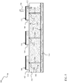
- FIG. 7 is a perspective diagram of an exemplary integrated bonding wire structure 700, including damping material 516 and integrated bonding wire structure 502.
- Damping material 516 can be added to integrated bonding wire structure 502 and can then be cured into a solid. Damping material 516 at least partially surrounds integrated bonding wire structure 502 and is at least partially interposed with bonding wire elements 600.
- Damping material 516 may include, for example, and without limitation, a resin based material, i.e., a curable resin. When cured, damping material 516 forms a coating that absorbs and attenuates ultrasonic energy.
- damping material 516 includes, for example, and without limitation, a plastic based material, an injectable material, tungsten powder, carbon powder, and other suitable materials for attenuating ultrasonic energy.
- FIG. 8 is a perspective diagram of an exemplary integrated bonding wire structure 700 (shown in FIG. 7 ) after trimming to design dimensions.
- structural base 620 shown in FIGs. 6 and 7
- damping material 516 defines first face 524, which can be positioned opposite second face 526.
- First face 524 can be oriented parallel to grid 610.
- FIG. 9 is a perspective diagram of an exemplary integrated bonding wire structure 700 (shown in FIGs. 7 and 8 ), forming phased array ultrasonic transducer 500.
- FIG. 9 further illustrates a transducer membrane 900 laminated to first face 524 and PCB 114 laminated to second face 526.
- Beneath transducer membrane 900 are a plurality of ultrasonic transducers 910 arranged in a matrix and respectively coupled to at least one of bonding wire elements 600 of integrated bonding wire structure 502.
- PCB 114 includes a plurality of circuits respectively coupled to opposite ends of at least one of bonding wire elements 600.
- FIG. 10 is a perspective cross-sectional diagram of an exemplary phased array ultrasonic transducer 500 shown in FIGs. 5 and 9.
- FIG. 10 illustrates bonding wire elements 600 of integrated bonding wire structure 700 coupling transducer membrane 900 and PCB 114.
- FIGs. 11-14 illustrate various shapes in which integrated bonding wire structure 502 may be formed.
- FIG. 11 is a cross-sectional diagram of an exemplary straight bonding wire structure 1100.
- FIG. 12 is a cross-sectional diagram of an exemplary straight bonding wire structure 1200 for a curved phased array ultrasonic transducer.
- FIG. 13 is a cross-sectional diagram of an exemplary 3-D shaped bonding wire structure 1300 for a 2-D phased array ultrasonic transducer.
- FIG. 14 is a cross-sectional diagram of another exemplary 3-D shaped bonding wire structure 1400 for a 3-D phased array ultrasonic transducer.
- other 3-D shaped bonding wire structures may be used.
- FIG. 15 is a flow diagram of an exemplary method 1500 of manufacturing phased array ultrasonic transducer 500 (shown in FIGs. 5-10 ).
- Method 1500 begins at a start step 1510.
- integrated bonding wire structure 502 is formed using a conductive material, such as, for example, copper.
- Additive manufacturing step 1520 includes, in certain embodiments, sequentially depositing layers of the conductive material to build up a plurality of bonding wire elements 600, or conductive columns on top of structural base 620, for example. Bonding wire elements 600 can be arranged in grid 610.
- damping material 516 is added to integrated bonding wire structure 502 to surround bonding wire elements 600, and interposed with bonding wire elements 600. Damping material 516 is then cured at a curing step 1540, forming a solid damping mass and further forming integrated bonding wire structure 700. Damping material 516 can be trimmed at a trimming step 1550 to design dimensions. Trimming step 1550, in certain embodiments, includes removing structural base 620, because each of bonding wire elements 600 are held in place by damping material 516. Trimming step 1550 defines first face 524 of damping material 516 and second face 526 of damping material 516. First face 524 is oriented parallel to grid 610 in which spacing among bonding wire elements 600 is defined. Second face 526 can be positioned opposite first face 524, where structural base 620 initially existed.
- transducer membrane 900 is laminated to first face 524 of damping material 516.
- Beneath transducer membrane 900 are a plurality of ultrasonic transducers 910 arranged in a matrix. At least one of ultrasonic transducers 910 is coupled to a corresponding bonding wire element of bonding wire elements 600.
- PCB 114 is laminated to second face 526 of damping material 516.
- PCB 114 includes a plurality of circuits for carrying AC signals to corresponding bonding wire elements, and ultimately conductively coupling to ultrasonic transducers 910 through integrated bonding wire structure 502.
- the method ends at an end step 1580.
- one or more of the steps may be omitted, additional steps may be performed, and/or the order of the steps may vary depending upon the application.
- an integrated bonding wire structure can be included that couples the ultrasonic transducers to a printed circuit board.
- the bonding wire structure can be manufactured by additive manufacturing techniques, sequentially depositing layers of a conductive material to form multiple bonding wire elements on top of a structural base.
- a damping material can be added to the bonding wire structure and cured.
- the damping material can be trimmed to design dimensions, including removal of the structural base for the bonding wire structure.
- the membrane for the ultrasonic transducers can be laminated on a first face of the damping material, and a printed circuit board is laminated to an opposite face.
- Additive manufacturing processes and systems include, for example, and without limitation, vat photopolymerization, powder bed fusion, binder jetting, material jetting, sheet lamination, material extrusion, directed energy deposition and hybrid systems. These processes and systems include, for example, and without limitation, SLA - Stereo lithography Apparatus, DLP - Digital Light Processing, 3SP - Scan, Spin, and Selectively Photocure, CLIP - Continuous Liquid Interface Production, SLS - Selective Laser Sintering, DMLS - Direct Metal Laser Sintering, SLM - Selective Laser Melting, EBM - Electron Beam Melting, SHS - Selective Heat Sintering, MJF - Multi-Jet Fusion, 3D Printing, Voxeljet, Polyjet, SCP - Smooth Curvatures Printing, MJM - Multi-Jet Modeling Projet, LOM - Laminated Object Manufacture, SDL - Selective Deposition Lamination, UAM - Ultrasonic Addi
- Additive manufacturing processes and systems employ materials including, for example, and without limitation, polymers, plastics, metals, ceramics, sand, glass, waxes, fibers, biological matter, composites, and hybrids of these materials. These materials may be used in these processes and systems in a variety of forms as appropriate for a given material and the process or system, including, for example, and without limitation, as liquids, solids, powders, sheets, foils, tapes, filaments, pellets, liquids, slurries, wires, atomized, pastes, and combinations of these forms.
- An exemplary technical effect of the methods, systems, and apparatus described herein can include at least one of: (a) positioning an ultrasonic damping mass between an ultrasonic transducer membrane and the PCB, (b) reducing ultrasonic energy passing through or absorbed into the PCB, (c) increasing contact density on the PCB for phased array ultrasonic transducers, (d) reducing number of PCB layers necessary for phased array ultrasonic transducers, (e) improving performance at high ultrasonic frequencies, (f) manufacturing a bonding wire structure integrated within the ultrasonic damping mass, (g) simplifying manufacture of integrated bonding wire structure through use of additive manufacturing techniques to form the bonding wire structure and the damping mass, (h) reducing manufacturing cost for phased array ultrasonic transducers through simplified additive manufacturing, (i) further reducing manufacturing cost for phased array ultrasonic transducers through reduced PCB layers, and (j) improving reliability of phased array ultrasonic transducers through reduced ultrasonic energy imparted on the PCB.
- Exemplary embodiments of methods, systems, and apparatus for phased array ultrasonic transducers are not limited to the specific embodiments described herein, but rather, components of systems and/or steps of the methods may be utilized independently and separately from other components and/or steps described herein.
- the methods may also be used in combination with other non-conventional bonding wire structures, and are not limited to practice with only the systems and methods as described herein.
- the exemplary embodiment can be implemented and utilized in connection with many other applications, equipment, and systems that may benefit from reduced cost, reduced complexity, commercial availability, improved reliability at high temperatures, and increased memory capacity.
- Approximating language may be applied to modify any quantitative representation that could permissibly vary without resulting in a change in the basic function to which it is related. Accordingly, a value modified by a term or terms, such as “about”, “approximately”, and “substantially”, are not to be limited to the precise value specified. In at least some instances, the approximating language may correspond to the precision of an instrument for measuring the value.
- range limitations may be combined and/or interchanged; such ranges are identified and include all the sub-ranges contained therein unless context or language indicates otherwise.
Abstract
Description
- The field of the disclosure relates generally to phased array ultrasonic transducers and, more particularly, to a phased array transducer with integrated bonding wire structure and a method of manufacture.
- In some present ultrasonic transducers, electrical energy is converted into ultrasonic waves, i.e., above 18 kilohertz (kHz), and vice versa. Ultrasonic transducers are sometimes referred to as ultrasonic transmitters, receivers, or transceivers, depending on their application. An ultrasonic transducer can include a membrane that oscillates in response to an alternating current (AC) signal applied to the ultrasonic transducer, or in response to a received ultrasonic signal. When transmitting, the membrane oscillates to produce an ultrasonic wave that propagates away from the membrane. When receiving, the membrane oscillates in a measurable manner, producing an AC signal in the ultrasonic transducer.
- Ultrasonic transducers are used in many fields for testing. For example, in medical fields, ultrasonic transducers are used for medical imaging. In other fields, ultrasonic transducers are used for nondestructive testing. Generally, ultrasonic transducers transmit an ultrasonic wave into an object. As the ultrasonic wave propagates through and reaches various features of the object, the ultrasonic wave can be partially reflected. The ultrasonic transducer detects the reflections. The reflections are interpreted based on the transmitted ultrasonic wave and the lapsed time between the transmission and receiving the reflections to analyze certain features of the object. Testing systems utilizing ultrasonic transducers can produce images, graphic displays, or measurements from the collected data.
- Single-element ultrasonic transducers can produce an ultrasonic wave characterized by its wavelength and its beam width, and propagating in a single direction. In some instances, ultrasonic testing, single-element ultrasonic transducers offer limited utility, because of their narrow unidirectional beam. In such instances, single-element ultrasonic transducers may be physically scanned, moved, or turned to sweep the ultrasonic beam over the area of the object being tested. In some instances, multiple ultrasonic transducers can be arranged in a phased array. Phased array arrangements vary widely according to their application, arrangements including one-dimensional (1-D) arrays, two-dimensional (2-D) arrays, and three-dimensional (3-D) arrays. Phased array ultrasonic transducers can facilitate electronically sweeping the ultrasonic beam over the area of the object being tested. Each ultrasonic transducer in the phased array can be individually controlled in amplitude, frequency, and phase, allowing the phased array ultrasonic transducer to produce a directed ultrasonic beam that can be electronically swept over the area of the object being tested.
- During operation, the ultrasonic energy emitted by the phased array ultrasonic transducer can be generally concentrated in the main beam. However, some amount of ultrasonic energy can be emitted in other, less desirable directions. Some conventional ultrasonic transducers and phased array ultrasonic transducers are manufactured such that the transducer membrane is in direct contact with a printed circuit board (PCB). The PCB includes an integrated circuit (IC) that carries the AC signals to and from each ultrasonic transducer in the phased array. Certain phased arrays require multiple PCB layers to provide sufficient contacts for the numerous ultrasonic transducers. Consequently, the PCB may absorb at least some of the undesired ultrasonic energy, reducing performance of the PCB itself and the phased array ultrasonic transducer.
- In one aspect, a phased array ultrasonic transducer includes a bonding wire structure, a damping material, a plurality of ultrasonic transducers, and a printed circuit board. The bonding wire structure includes a plurality of bonding wire elements. The damping material surrounds the bonding wire structure and is interposed with the plurality of bonding wire elements. The plurality of ultrasonic transducers is arranged in a matrix beneath a membrane, each of the plurality of ultrasonic transducers being coupled to a corresponding bonding wire element of the plurality of bonding wire elements. The printed circuit board includes a plurality of circuits. Each of the plurality of circuits is coupled to a corresponding bonding wire element of the plurality of bonding wire elements.
- In another aspect, a method of manufacturing a phased array ultrasonic transducer is provided. The method includes forming a bonding wire structure of conductive material. The bonding wire structure includes a plurality of bonding wire elements arranged in a grid and coupled to a structural base. The method further includes positioning a damping material surrounding and interposed with the plurality of bonding wire elements. The damping material defines a first face that is substantially parallel to the grid and a second face that is opposite the first face. The method further includes trimming the structural base from the phased array ultrasonic transducer.
- In yet another aspect a phased array ultrasonic transducer is provided. The phased array ultrasonic transducer includes a bonding wire structure, a damping material, a plurality of ultrasonic transducers, and a printed circuit board. The bonding wire structure includes a plurality of bonding wire elements formed by sequentially depositing a conductive material in layers on a structural base. The plurality of bonding wire elements is arranged in a grid. The damping material extends across the bonding wire structure to surround the bonding wire structure. The damping material is interposed with the plurality of bonding wire elements. The damping material defines a first face that is substantially parallel to the grid of bonding wire elements. The plurality of ultrasonic transducers is arranged in a matrix beneath a membrane. Each of the plurality of ultrasonic transducers is coupled to a corresponding bonding wire element of the plurality of bonding wire elements. The membrane is laminated to the first face of the damping material. The printed circuit board includes a plurality of circuits, where each of the plurality of circuits is coupled to a corresponding bonding wire element of the plurality of bonding wire elements. The printed circuit board is laminated to a second face of the damping material, the second face defined opposite the first face.
- These and other features, aspects, and advantages of the present disclosure will become better understood when the following detailed description is read with reference to the accompanying drawings in which like characters represent like parts throughout the drawings, wherein:
-
FIG. 1 is a cross-sectional diagram of a conventional phased array ultrasonic transducer; -
FIG. 2 is a diagram of an exemplary 1-D phased array ultrasonic transducer; -
FIG. 3 is a diagram of an exemplary 2-D phased array ultrasonic transducer; -
FIG. 4 is a diagram of an exemplary 3-D phased array ultrasonic transducer; -
FIG. 5 is a diagram of the exemplary phased array ultrasonic transducer with integrated bonding wire structure; -
FIG. 6 is a perspective diagram of an exemplary 3D-printed integrated bonding wire structure for the phased array ultrasonic transducer shown inFIG. 5 ; -
FIG. 7 is a perspective diagram of the integrated bonding wire structure, shown inFIG. 6 , with damping material added; -
FIG. 8 is a perspective diagram of the integrated bonding wire structure and damping material shown inFIGs. 6 and 7 after trimming to design dimensions; -
FIG. 9 is a perspective diagram of the trimmed integrated bonding wire structure and damping material, shown inFIG. 8 , having a transducer membrane laminate and a PCB laminate; -
FIG. 10 is a perspective cross-sectional diagram of the phased array ultrasonic transducer shown inFIG. 9 ; -
FIG. 11 is a cross-sectional diagram of an exemplary straight bonding wire structure; -
FIG. 12 is a cross-sectional diagram of an exemplary straight bonding wire structure for a curved phased array ultrasonic transducer; -
FIG. 13 is a cross-sectional diagram of an exemplary 3-D shaped bonding wire structure for a 2-D phased array ultrasonic transducer; -
FIG. 14 is a cross-sectional diagram of another exemplary 3-D shaped bonding wire structure for a 3-D phased array ultrasonic transducer; and -
FIG. 15 is a flow diagram of an exemplary method of manufacturing the phased array ultrasonic transducer shown inFIG. 10 . - Unless otherwise indicated, the drawings provided herein are meant to illustrate features of embodiments of this disclosure. These features are believed to be applicable in a wide variety of systems comprising one or more embodiments of this disclosure. As such, the drawings are not meant to include all conventional features known by those of ordinary skill in the art to be required for the practice of the embodiments disclosed herein.
- The present disclosure describes ultrasonic transducers and techniques for manufacturing a phased array ultrasonic transducer with integrated bonding wire. Ultrasonic transducers can be mounted indirectly to or directly to a printed circuit board that drives the ultrasonic transducers, which can expose the printed circuit board to some amount of ultrasonic energy during operation. As described more fully below, some embodiments of the present disclosure provide a bonding wire structure that connects the ultrasonic transducer to the printed circuit board. The bonding wire structure can be surrounded by an ultrasonic damping material that reduces the amount of ultrasonic energy that reaches the printed circuit board. Such a bonding wire structure and damping material may be manufactured using additive manufacturing techniques. For example, a bonding wire structure can be 3D-printed using a conductive material. A resin-based damping material is then applied to the bonding wire structure and cured, resulting in an integrated bonding wire structure. The integrated bonding wire structure can then be trimmed and mounted between ultrasonic transducers and a printed circuit board. Other embodiments are within the scope of the present disclosure.
- Embodiments of the present disclosure relate to phased array ultrasonic transducers. More specifically, the phased array ultrasonic transducers described herein include an integrated bonding wire structure that can couple the ultrasonic transducers to a printed circuit board. The bonding wire structure may be manufactured by additive manufacturing techniques, sequentially depositing layers of a conductive material to form multiple bonding wire elements on top of a structural base. A damping material is then added to the bonding wire structure and cured. The damping material can be trimmed to design dimensions, including removal of the structural base for the bonding wire structure. The membrane for the ultrasonic transducers may be laminated on a first face of the damping material, and a printed circuit board can be laminated to an opposite face.
-
FIG. 1 is a cross-sectional diagram of an embodiment of a conventional phased arrayultrasonic transducer 100. Phased arrayultrasonic transducer 100 can includetransducers ultrasonic transducer 100 may include additional or fewer transducers (not shown), however, for clarity,FIG. 1 illustrates only a portion of phased arrayultrasonic transducer 100.Transducers respective membranes transducers Transducers -
Transducers respective contacts PCB 114 can include multiple circuits (not shown) for carrying signals to and from each oftransducers transducers PCB 114 can be filled by afiller material 122.PCB 114 may include a rigid PCB or a flexible PCB, and may further include one or more PCB layers to accommodate the necessary circuits and contacts fortransducers - Phased array
ultrasonic transducer 100 can include a dampingmaterial 124 fixed to a side, for example, the back side ofPCB 114. Properties of dampingmaterial 124 further define the operating characteristics of phased arrayultrasonic transducer 100, including frequency response and sensitivity. During operation, each oftransducers ultrasonic wave 126 that propagates away fromrespective membranes PCB 114 and dampingmaterial 124. Such ultrasonic energy is illustrated asultrasonic wave 128. Dampingmaterial 124 attenuatesultrasonic wave 128. -
FIG. 2 is a diagram of an exemplary 1-D phased arrayultrasonic transducer 200. Phased arrayultrasonic transducer 200 includes a plurality ofultrasonic transducers 210 arranged in arow 220. Phased arrayultrasonic transducer 200, in certain embodiments, may be formed at least partially by dicing a larger rectangular transducer. During operation, the ultrasonic beam generated by phased arrayultrasonic transducer 200 is steerable in a single plane. -
FIG. 3 is a diagram of an exemplary 2-D phased arrayultrasonic transducer 300. Phased arrayultrasonic transducer 300 includes a plurality ofultrasonic transducers 310 arranged inrows 320 andcolumns 330 to form a grid. During operation, the ultrasonic beam generated by phased arrayultrasonic transducer 300 can be steerable in three dimensions. -
FIG. 4 is a diagram of an exemplary 3-D phased arrayultrasonic transducer 400. Phased arrayultrasonic transducer 400 includes a plurality ofultrasonic transducers 410 arranged inrows 420 andcolumns 430, also forming a grid. Each ofrows 420 ofultrasonic transducers 410 is curved, allowing the generated ultrasonic beam to conform to the curve or the geometry of an object being tested. The generated ultrasonic beam is further steerable in three dimensions. In other embodiments,rows 420 ofultrasonic transducers 410 may be curved in one direction and change to another, for example, in an "S" configuration or another shape to enable the ultrasonic beam to conform to the curve or the geometry of the object being tested. -
FIG. 5 is a diagram of the exemplary phased arrayultrasonic transducer 500 with an integratedbonding wire structure 502. Integratedbonding wire structure 502 includes a plurality ofbonding wire elements PCB 114 andtransducers Bonding wire elements PCB 114 totransducers Transducers bonding wire elements contacts - In certain embodiments,
bonding wire elements bonding wire structure 502 includes a plurality of conductive cones, where the broad end is coupled to a transducer, such astransducers PCB 114. In another embodiment, integratedbonding wire structure 502 includes a plurality of conductive cylinders. - Phased array
ultrasonic transducer 500 can include a dampingmaterial 516 that surrounds and is interposed withbonding wire elements transducers material 516 can be filled by afiller material 518. During operation, each oftransducers ultrasonic wave 520 that propagates away fromrespective membranes material 516, where it is attenuated before reachingPCB 114. Such ultrasonic energy is illustrated asultrasonic wave 522. Dampingmaterial 516 defines afirst face 524 to whichtransducers material 516 further defines asecond face 526.PCB 114 can be coupled tosecond face 526. Phased arrayultrasonic transducer 500 includesfirst face 524 andsecond face 526 that can be positioned oppositefirst face 524. In alternative embodiments,first face 524 andsecond face 526 may be configured otherwise. For example,second face 526 may be orthogonal and adjacent tofirst face 524. -
FIG. 6 is a perspective diagram of an exemplary 3D-printed integratedbonding wire structure 502 for phased array ultrasonic transducer 500 (shown inFIG. 5 ). Integratedbonding wire structure 502 is composed of a conductive material, such as, for example, and without limitation, copper, tin, aluminum, tungsten, or gold. Integratedbonding wire structure 502 includes a plurality ofbonding wire elements 600 arranged in agrid 610.Grid 610 may have any suitable spacing for a given application. For example, in one embodiment,bonding wire elements 600 are arranged on a 1 millimeter (mm) grid. In another embodiment, for example,bonding wire elements 600 are arranged on a 0.5 mm grid. - In some embodiments, each of
bonding wire elements 600, such asbonding wire elements FIG. 5 ) is configured to couple an ultrasonic transducer to a PCB, such as PCB 114 (shown inFIGs. 1 and5 ). In other embodiment, one or more bonding wire elements are configured to couple with an ultrasonic transducer PCB, such asPCB 114.Bonding wire elements 600 each may include a conductive column extending from astructural base 620. Integratedbonding wire structure 502 is at least partially formed using an additive manufacturing technique, sometimes referred to as 3D printing. More specifically, integratedbonding wire structure 502 is formed by depositing sequential layers of conductive material to form each ofbonding wire elements 600. Such techniques include, for example, and without limitation, metal powder injection, fused deposition modeling, fused filament fabrication, robocasting, stereolithography, digital light processing, powder bed and inkjet head 3D printing, electron beam melting, selective laser melting, selective heat sintering, selective laser sintering, direct metal laser sintering, laminated object manufacturing, directed energy deposition, and electron beam freeform fabrication. The conductive material can be deposited in layers until a desired length of the conductive columns is reached. In certain embodiments, the conductive column length is 15 mm. The length of the conductive columns may vary based on the application of phased arrayultrasonic transducer 500. The shape of each ofbonding wire elements 600 may also vary based on the application. In certain embodiments,bonding wire elements 600 are round. In alternative embodiments,bonding wire elements 600 may be rectangular, conical, or any other suitable shape. Further,bonding wire elements 600 can be formed to match the geometry of the transducer surface. In certain embodiments,bonding wire elements 600 follow a defined 3-D spline. -
FIG. 7 is a perspective diagram of an exemplary integratedbonding wire structure 700, including dampingmaterial 516 and integratedbonding wire structure 502. Dampingmaterial 516 can be added to integratedbonding wire structure 502 and can then be cured into a solid. Dampingmaterial 516 at least partially surrounds integratedbonding wire structure 502 and is at least partially interposed withbonding wire elements 600. Dampingmaterial 516 may include, for example, and without limitation, a resin based material, i.e., a curable resin. When cured, dampingmaterial 516 forms a coating that absorbs and attenuates ultrasonic energy. In alternative embodiments, dampingmaterial 516 includes, for example, and without limitation, a plastic based material, an injectable material, tungsten powder, carbon powder, and other suitable materials for attenuating ultrasonic energy. -
FIG. 8 is a perspective diagram of an exemplary integrated bonding wire structure 700 (shown inFIG. 7 ) after trimming to design dimensions. During trimming, structural base 620 (shown inFIGs. 6 and 7 ) can be removed fromsecond face 526 of dampingmaterial 516. Additional, dampingmaterial 516 definesfirst face 524, which can be positioned oppositesecond face 526.First face 524 can be oriented parallel togrid 610. -
FIG. 9 is a perspective diagram of an exemplary integrated bonding wire structure 700 (shown inFIGs. 7 and 8 ), forming phased arrayultrasonic transducer 500.FIG. 9 further illustrates atransducer membrane 900 laminated tofirst face 524 andPCB 114 laminated tosecond face 526. Beneathtransducer membrane 900 are a plurality ofultrasonic transducers 910 arranged in a matrix and respectively coupled to at least one ofbonding wire elements 600 of integratedbonding wire structure 502. Likewise,PCB 114 includes a plurality of circuits respectively coupled to opposite ends of at least one ofbonding wire elements 600. -
FIG. 10 is a perspective cross-sectional diagram of an exemplary phased arrayultrasonic transducer 500 shown inFIGs. 5 and9. FIG. 10 illustratesbonding wire elements 600 of integratedbonding wire structure 700coupling transducer membrane 900 andPCB 114. -
FIGs. 11-14 illustrate various shapes in which integratedbonding wire structure 502 may be formed.FIG. 11 is a cross-sectional diagram of an exemplary straightbonding wire structure 1100.FIG. 12 is a cross-sectional diagram of an exemplary straightbonding wire structure 1200 for a curved phased array ultrasonic transducer.FIG. 13 is a cross-sectional diagram of an exemplary 3-D shapedbonding wire structure 1300 for a 2-D phased array ultrasonic transducer.FIG. 14 is a cross-sectional diagram of another exemplary 3-D shapedbonding wire structure 1400 for a 3-D phased array ultrasonic transducer. In additional embodiments, other 3-D shaped bonding wire structures may be used. -
FIG. 15 is a flow diagram of anexemplary method 1500 of manufacturing phased array ultrasonic transducer 500 (shown inFIGs. 5-10 ).Method 1500 begins at astart step 1510. At anadditive manufacturing step 1520, integratedbonding wire structure 502 is formed using a conductive material, such as, for example, copper.Additive manufacturing step 1520 includes, in certain embodiments, sequentially depositing layers of the conductive material to build up a plurality ofbonding wire elements 600, or conductive columns on top ofstructural base 620, for example.Bonding wire elements 600 can be arranged ingrid 610. - At a second
additive manufacturing step 1530, dampingmaterial 516 is added to integratedbonding wire structure 502 to surroundbonding wire elements 600, and interposed withbonding wire elements 600. Dampingmaterial 516 is then cured at acuring step 1540, forming a solid damping mass and further forming integratedbonding wire structure 700. Dampingmaterial 516 can be trimmed at atrimming step 1550 to design dimensions. Trimmingstep 1550, in certain embodiments, includes removingstructural base 620, because each ofbonding wire elements 600 are held in place by dampingmaterial 516. Trimmingstep 1550 definesfirst face 524 of dampingmaterial 516 andsecond face 526 of dampingmaterial 516.First face 524 is oriented parallel togrid 610 in which spacing amongbonding wire elements 600 is defined.Second face 526 can be positioned oppositefirst face 524, wherestructural base 620 initially existed. - At a
first lamination step 1560,transducer membrane 900 is laminated tofirst face 524 of dampingmaterial 516. Beneathtransducer membrane 900 are a plurality ofultrasonic transducers 910 arranged in a matrix. At least one ofultrasonic transducers 910 is coupled to a corresponding bonding wire element ofbonding wire elements 600. - At a
second lamination step 1570,PCB 114 is laminated tosecond face 526 of dampingmaterial 516.PCB 114 includes a plurality of circuits for carrying AC signals to corresponding bonding wire elements, and ultimately conductively coupling toultrasonic transducers 910 through integratedbonding wire structure 502. - The method ends at an
end step 1580. In various embodiments ofmethod 1500, one or more of the steps may be omitted, additional steps may be performed, and/or the order of the steps may vary depending upon the application. - In the embodiments of the above described phased array ultrasonic transducers, an integrated bonding wire structure can be included that couples the ultrasonic transducers to a printed circuit board. The bonding wire structure can be manufactured by additive manufacturing techniques, sequentially depositing layers of a conductive material to form multiple bonding wire elements on top of a structural base. A damping material can be added to the bonding wire structure and cured. The damping material can be trimmed to design dimensions, including removal of the structural base for the bonding wire structure. The membrane for the ultrasonic transducers can be laminated on a first face of the damping material, and a printed circuit board is laminated to an opposite face.
- Additive manufacturing processes and systems include, for example, and without limitation, vat photopolymerization, powder bed fusion, binder jetting, material jetting, sheet lamination, material extrusion, directed energy deposition and hybrid systems. These processes and systems include, for example, and without limitation, SLA - Stereo lithography Apparatus, DLP - Digital Light Processing, 3SP - Scan, Spin, and Selectively Photocure, CLIP - Continuous Liquid Interface Production, SLS - Selective Laser Sintering, DMLS - Direct Metal Laser Sintering, SLM - Selective Laser Melting, EBM - Electron Beam Melting, SHS - Selective Heat Sintering, MJF - Multi-Jet Fusion, 3D Printing, Voxeljet, Polyjet, SCP - Smooth Curvatures Printing, MJM - Multi-Jet Modeling Projet, LOM - Laminated Object Manufacture, SDL - Selective Deposition Lamination, UAM - Ultrasonic Additive Manufacturing, FFF - Fused Filament Fabrication, FDM - Fused Deposition Modeling, LMD - Laser Metal Deposition, LENS - Laser Engineered Net Shaping, DMD - Direct Metal Deposition, Hybrid Systems, and combinations of these processes and systems. These processes and systems may employ, for example, and without limitation, all forms of electromagnetic radiation, heating, sintering, melting, curing, binding, consolidating, pressing, embedding, and combinations thereof.
- Additive manufacturing processes and systems employ materials including, for example, and without limitation, polymers, plastics, metals, ceramics, sand, glass, waxes, fibers, biological matter, composites, and hybrids of these materials. These materials may be used in these processes and systems in a variety of forms as appropriate for a given material and the process or system, including, for example, and without limitation, as liquids, solids, powders, sheets, foils, tapes, filaments, pellets, liquids, slurries, wires, atomized, pastes, and combinations of these forms.
- An exemplary technical effect of the methods, systems, and apparatus described herein can include at least one of: (a) positioning an ultrasonic damping mass between an ultrasonic transducer membrane and the PCB, (b) reducing ultrasonic energy passing through or absorbed into the PCB, (c) increasing contact density on the PCB for phased array ultrasonic transducers, (d) reducing number of PCB layers necessary for phased array ultrasonic transducers, (e) improving performance at high ultrasonic frequencies, (f) manufacturing a bonding wire structure integrated within the ultrasonic damping mass, (g) simplifying manufacture of integrated bonding wire structure through use of additive manufacturing techniques to form the bonding wire structure and the damping mass, (h) reducing manufacturing cost for phased array ultrasonic transducers through simplified additive manufacturing, (i) further reducing manufacturing cost for phased array ultrasonic transducers through reduced PCB layers, and (j) improving reliability of phased array ultrasonic transducers through reduced ultrasonic energy imparted on the PCB.
- Exemplary embodiments of methods, systems, and apparatus for phased array ultrasonic transducers are not limited to the specific embodiments described herein, but rather, components of systems and/or steps of the methods may be utilized independently and separately from other components and/or steps described herein. For example, the methods may also be used in combination with other non-conventional bonding wire structures, and are not limited to practice with only the systems and methods as described herein. Rather, the exemplary embodiment can be implemented and utilized in connection with many other applications, equipment, and systems that may benefit from reduced cost, reduced complexity, commercial availability, improved reliability at high temperatures, and increased memory capacity.
- In the preceding specification and the claims, a number of terms are referenced that have the following meanings.
- The singular forms "a", "an", and "the" include plural references unless the context clearly dictates otherwise.
- "Optional" or "optionally" means that the subsequently described event or circumstance may or may not occur, and that the description includes instances where the event occurs and instances where it does not.
- Approximating language, as used herein throughout the specification and claims, may be applied to modify any quantitative representation that could permissibly vary without resulting in a change in the basic function to which it is related. Accordingly, a value modified by a term or terms, such as "about", "approximately", and "substantially", are not to be limited to the precise value specified. In at least some instances, the approximating language may correspond to the precision of an instrument for measuring the value. Here and throughout the specification and claims, range limitations may be combined and/or interchanged; such ranges are identified and include all the sub-ranges contained therein unless context or language indicates otherwise.
- Although specific features of various embodiments of the disclosure may be shown in some drawings and not in others, this is for convenience only. In accordance with the principles of the disclosure, any feature of a drawing may be referenced and/or claimed in combination with any feature of any other drawing.
- This written description uses examples to disclose the embodiments, including the best mode, and also to enable any person skilled in the art to practice the embodiments, including making and using any devices or systems and performing any incorporated methods. The patentable scope of the disclosure is defined by the claims, and may include other examples that occur to those skilled in the art. Such other examples are intended to be within the scope of the claims if they have structural elements that do not differ from the literal language of the claims, or if they include equivalent structural elements with insubstantial differences from the literal language of the claims.
- Various aspects and embodiments of the present invention are defined by the following numbered clauses:
- 1. A phased array ultrasonic transducer comprising:
- a bonding wire structure comprising a plurality of bonding wire elements;
- a damping material surrounding the bonding wire structure and interposed with the plurality of bonding wire elements;
- a plurality of ultrasonic transducers arranged in a matrix, each of said ultrasonic transducers coupled to at least one of said plurality of bonding wire elements; and
- a printed circuit board comprising a plurality of circuits, each said circuit coupled to a wire element of said plurality of bonding wire elements.
- 2. The phased array ultrasonic transducer of Clause 1, wherein said printed circuit board further comprises a flexible printed circuit board.
- 3. The phased array ultrasonic transducer of Clause 1 or Clause 2, wherein each of said plurality of bonding wire elements comprises a conductive column.
- 4. The phased array ultrasonic transducer of any preceding Clause, wherein said conductive column comprises copper.
- 5. The phased array ultrasonic transducer of any preceding Clause, wherein each of said plurality of bonding wire elements comprises a conductive cylinder comprising a first end coupled to a structural base.
- 6. The phased array ultrasonic transducer of any preceding Clause, wherein each of said plurality of bonding wire elements comprises a conductive cone comprising a broad end coupled to a corresponding one of said plurality of ultrasonic transducers, and a narrow end coupled to said printed circuit board.
- 7. The phased array ultrasonic transducer of any preceding Clause, wherein said damping material defines:
- a first face coupled to said plurality of ultrasonic transducers and to a membrane; and
- a second face opposite said first face and coupled to said printed circuit board.
- 8. A method of manufacturing a phased array ultrasonic transducer, said method comprising:
- forming a bonding wire structure of conductive material, wherein the bonding wire structure includes a plurality of bonding wire elements arranged in a grid and coupled to a structural base; and
- positioning a damping material to surround and to interpose with the plurality of bonding wire elements, wherein the damping material defines a first face that is substantially parallel to the grid and to a second face that is opposite the first face.
- 9. The method of any preceding Clause, further comprising curing the damping material.
- 10. The method of any preceding Clause, further comprising trimming the damping material to predefined dimensions.
- 11. The method of any preceding Clause, further comprising coupling a plurality of ultrasonic transducers to the first face, such that the plurality of ultrasonic transducers are arranged in a matrix beneath a membrane, wherein each of the plurality of ultrasonic transducers is coupled to a corresponding one of the plurality of bonding wire elements.
- 12. The method of any preceding Clause, wherein coupling the plurality of ultrasonic transducers to the first face comprises laminating the membrane to the first face.
- 13. The method of any preceding Clause, further comprising coupling a printed circuit board to the second face, wherein the printed circuit board includes a plurality of circuits that are each coupled to a corresponding one of the plurality of bonding wire elements.
- 14. The method of any preceding Clause, wherein coupling the printed circuit board to the second face comprises laminating the printed circuit board to the second face.
- 15. The method of any preceding Clause, wherein forming the bonding wire structure comprises sequentially depositing the conductive material in layers using an additive manufacturing technique.
- 16. The method of any preceding Clause, further comprising trimming the structural base from the phased array ultrasonic transducer.
- 17. A phased array ultrasonic transducer comprising:
- a bonding wire structure comprising a plurality of bonding wire elements formed by sequentially depositing a conductive material in layers on a structural base such that said plurality of bonding wire elements are arranged in a grid of bonding wire elements;
- a damping material extending across said bonding wire structure such that said bonding wire structure is surrounded and such that said damping material is interposed with said plurality of bonding wire elements, wherein said damping material defines a first face that is substantially parallel to the grid of bonding wire elements;
- a plurality of ultrasonic transducers arranged in a matrix beneath a membrane, each of said plurality of ultrasonic transducers is coupled to a corresponding one of said plurality of bonding wire elements, and wherein said membrane is laminated to said first face of said damping material; and
- a printed circuit board comprising a plurality of circuits, each of said plurality of circuits coupled to a corresponding one of said plurality of bonding wire elements, said printed circuit board laminated to a second face of said damping material, said second face defined opposite said first face.
- 18. The phased array ultrasonic transducer of any preceding Clause, wherein said damping material comprises a curable resin.
- 19. The phased array ultrasonic transducer of any preceding Clause, wherein said first face and said second face of said damping material are further defined by trimming of said damping material to predefined dimensions.
- 20. The phased array ultrasonic transducer of any preceding Clause, wherein said bonding wire structure comprises a plurality of conductive cones, each conductive cone comprising a broad end coupled to a corresponding one of said plurality of ultrasonic transducers, and a narrow end coupled to said printed circuit board.
- 21. The phased array ultrasonic transducer of any preceding Clause, wherein said printed circuit board comprises a flexible printed circuit board.
Claims (15)
- A phased array ultrasonic transducer (100;200;300;400;500) comprising:a bonding wire structure (502;700;1100;1200;1300;1400) comprising a plurality of bonding wire elements (504,506,508;600);a damping material (124;516) surrounding the bonding wire structure and interposed with the plurality of bonding wire elements;a plurality of ultrasonic transducers (102,104,106;210;310;410;910) arranged in a matrix, each of said ultrasonic transducers coupled to at least one of said plurality of bonding wire elements; anda printed circuit board (114) comprising a plurality of circuits, each said circuit coupled to a wire element of said plurality of bonding wire elements.
- The phased array ultrasonic transducer (100;200;300;400;500) of Claim 1, wherein said printed circuit board (114) further comprises a flexible printed circuit board.
- The phased array ultrasonic transducer (100;200;300;400;500) of Claim 1 or Claim 2, wherein each of said plurality of bonding wire elements (504,506,508;600) comprises a conductive column.
- The phased array ultrasonic transducer (100;200;300;400;500) of any preceding Claim, wherein said conductive column comprises copper.
- The phased array ultrasonic transducer (100;200;300;400;500) of any preceding Claim, wherein each of said plurality of bonding wire elements (504,506,508;600) comprises a conductive cylinder comprising a first end coupled to a structural base (620).
- The phased array ultrasonic transducer (100;200;300;400;500) of any preceding Claim, wherein each of said plurality of bonding wire elements (504,506,508;600) comprises a conductive cone comprising a broad end coupled to a corresponding one of said plurality of ultrasonic transducers (102,104,106;210;310;410;910), and a narrow end coupled to said printed circuit board (114).
- The phased array ultrasonic transducer (100;200;300;400;500) of any preceding Claim, wherein said damping material (124;516) defines:a first face (524) coupled to said plurality of ultrasonic transducers (102,104,106;210;310;410;910) and to a membrane (108,110,112;900); anda second face (526) opposite said first face and coupled to said printed circuit board (114).
- A method (1500) of manufacturing a phased array ultrasonic transducer (100;200;300;400;500), said method comprising:forming (1520) a bonding wire structure (502;700;1100;1200;1300;1400) of conductive material, wherein the bonding wire structure includes a plurality of bonding wire elements (504,506,508;600) arranged in a grid and coupled to a structural base (620); andpositioning (1530) a damping material (124;516) to surround and to interpose with the plurality of bonding wire elements, wherein the damping material defines a first face (524) that is substantially parallel to the grid and to a second face (526) that is opposite the first face.
- The method (1500) of Claim 8, further comprising curing the damping material (124;516).
- The method (1500) of Claim 8 or Claim 9, further comprising trimming (1550) the damping material (124;516) to predefined dimensions.
- The method (1500) of any of Claims 8 to 10, further comprising coupling (1560) a plurality of ultrasonic transducers (102,104,106;210;310;410;910) to the first face (524), such that the plurality of ultrasonic transducers are arranged in a matrix beneath a membrane (108,110,112;900), wherein each of the plurality of ultrasonic transducers is coupled to a corresponding one of the plurality of bonding wire elements (504,506,508;600).
- The method (1500) of any of Claims 8 to 11, wherein coupling (1560) the plurality of ultrasonic transducers (102,104,106;210;310;410;910) to the first face (524) comprises laminating the membrane (108,110,112;900) to the first face.
- The method (1500) of any of Claims 8 to 12, further comprising coupling (1570) a printed circuit board (114) to the second face (526), wherein the printed circuit board includes a plurality of circuits that are each coupled to a corresponding one of the plurality of bonding wire elements (504,506,508;600).
- The method (1500) of any of Claims 8 to 13, wherein coupling (1570) the printed circuit board (114) to the second face (526) comprises laminating the printed circuit board to the second face.
- The method (1500) of any of Claims 8 to 14, wherein forming (1520) the bonding wire structure (502;700;1100;1200;1300;1400) comprises sequentially depositing the conductive material in layers using an additive manufacturing technique.
Applications Claiming Priority (2)
| Application Number | Priority Date | Filing Date | Title |
|---|---|---|---|
| US201662337075P | 2016-05-16 | 2016-05-16 | |
| US15/595,122 US11471911B2 (en) | 2016-05-16 | 2017-05-15 | Phased array ultrasonic transducer and method of manufacture |
Publications (1)
| Publication Number | Publication Date |
|---|---|
| EP3246701A1 true EP3246701A1 (en) | 2017-11-22 |
Family
ID=58714958
Family Applications (1)
| Application Number | Title | Priority Date | Filing Date |
|---|---|---|---|
| EP17171249.0A Pending EP3246701A1 (en) | 2016-05-16 | 2017-05-16 | Ultrasonic transducer array and method of manufacture |
Country Status (2)
| Country | Link |
|---|---|
| US (1) | US11471911B2 (en) |
| EP (1) | EP3246701A1 (en) |
Cited By (1)
| Publication number | Priority date | Publication date | Assignee | Title |
|---|---|---|---|---|
| DE102020102248A1 (en) | 2020-01-30 | 2021-08-05 | Sick Engineering Gmbh | Basic transducer element for an ultrasonic transducer |
Families Citing this family (6)
| Publication number | Priority date | Publication date | Assignee | Title |
|---|---|---|---|---|
| US11090688B2 (en) * | 2016-08-10 | 2021-08-17 | The Ultran Group, Inc. | Gas matrix piezoelectric ultrasound array transducer |
| US10104759B2 (en) | 2016-11-29 | 2018-10-16 | Nxp Usa, Inc. | Microelectronic modules with sinter-bonded heat dissipation structures and methods for the fabrication thereof |
| US10485091B2 (en) * | 2016-11-29 | 2019-11-19 | Nxp Usa, Inc. | Microelectronic modules with sinter-bonded heat dissipation structures and methods for the fabrication thereof |
| CN108770215B (en) * | 2018-07-27 | 2023-06-02 | 四川长虹智能制造技术有限公司 | 3D printed circuit board processing method and spray head thereof |
| EP3680030A1 (en) * | 2019-01-14 | 2020-07-15 | Continental Automotive GmbH | Ultrasonic transducer device and air suspension device comprising the ultrasonic transducer device |
| JP7309552B2 (en) * | 2019-09-19 | 2023-07-18 | 新光電気工業株式会社 | Backing material, ultrasonic probe |
Citations (3)
| Publication number | Priority date | Publication date | Assignee | Title |
|---|---|---|---|---|
| US5267221A (en) * | 1992-02-13 | 1993-11-30 | Hewlett-Packard Company | Backing for acoustic transducer array |
| US6467138B1 (en) * | 2000-05-24 | 2002-10-22 | Vermon | Integrated connector backings for matrix array transducers, matrix array transducers employing such backings and methods of making the same |
| US20150311424A1 (en) * | 2014-04-24 | 2015-10-29 | General Electric Company | Piezoelectric composite and method of forming same |
Family Cites Families (10)
| Publication number | Priority date | Publication date | Assignee | Title |
|---|---|---|---|---|
| US20040123666A1 (en) | 2002-12-31 | 2004-07-01 | Ao Xiaolei S. | Ultrasonic damping material |
| JP2007513563A (en) | 2003-12-04 | 2007-05-24 | コーニンクレッカ フィリップス エレクトロニクス エヌ ヴィ | Apparatus and method for mounting an IC mounted sensor with a high attenuation backing |
| JP5175853B2 (en) * | 2006-09-25 | 2013-04-03 | コーニンクレッカ フィリップス エレクトロニクス エヌ ヴィ | Flip chip interconnect through chip vias |
| US7808157B2 (en) * | 2007-03-30 | 2010-10-05 | Gore Enterprise Holdings, Inc. | Ultrasonic attenuation materials |
| US9788813B2 (en) | 2010-10-13 | 2017-10-17 | Maui Imaging, Inc. | Multiple aperture probe internal apparatus and cable assemblies |
| US8207652B2 (en) * | 2009-06-16 | 2012-06-26 | General Electric Company | Ultrasound transducer with improved acoustic performance |
| JP2011250119A (en) * | 2010-05-26 | 2011-12-08 | Toshiba Corp | Ultrasonic probe |
| JP5620345B2 (en) * | 2010-06-23 | 2014-11-05 | 株式会社東芝 | Ultrasonic transducer and manufacturing method thereof |
| US9035532B2 (en) | 2012-11-02 | 2015-05-19 | University Of Windsor | Ultrasonic sensor microarray and method of manufacturing same |
| DE102013101097A1 (en) | 2013-02-04 | 2014-08-21 | Ge Sensing & Inspection Technologies Gmbh | Method for contacting an ultrasonic transducer; Ultrasonic transducer component with contacted ultrasonic transducer for use in an ultrasonic probe; Ultrasonic test head and device for non-destructive testing of a test specimen by means of ultrasound |
-
2017
- 2017-05-15 US US15/595,122 patent/US11471911B2/en active Active
- 2017-05-16 EP EP17171249.0A patent/EP3246701A1/en active Pending
Patent Citations (3)
| Publication number | Priority date | Publication date | Assignee | Title |
|---|---|---|---|---|
| US5267221A (en) * | 1992-02-13 | 1993-11-30 | Hewlett-Packard Company | Backing for acoustic transducer array |
| US6467138B1 (en) * | 2000-05-24 | 2002-10-22 | Vermon | Integrated connector backings for matrix array transducers, matrix array transducers employing such backings and methods of making the same |
| US20150311424A1 (en) * | 2014-04-24 | 2015-10-29 | General Electric Company | Piezoelectric composite and method of forming same |
Cited By (1)
| Publication number | Priority date | Publication date | Assignee | Title |
|---|---|---|---|---|
| DE102020102248A1 (en) | 2020-01-30 | 2021-08-05 | Sick Engineering Gmbh | Basic transducer element for an ultrasonic transducer |
Also Published As
| Publication number | Publication date |
|---|---|
| US11471911B2 (en) | 2022-10-18 |
| US20170326592A1 (en) | 2017-11-16 |
Similar Documents
| Publication | Publication Date | Title |
|---|---|---|
| US11471911B2 (en) | Phased array ultrasonic transducer and method of manufacture | |
| Hu et al. | Stretchable ultrasonic transducer arrays for three-dimensional imaging on complex surfaces | |
| US6467138B1 (en) | Integrated connector backings for matrix array transducers, matrix array transducers employing such backings and methods of making the same | |
| JP6208933B2 (en) | Transducer structure for transducer probe and method of manufacturing the same | |
| CN101495247B (en) | Ultrasound transducer featuring a pitch independent interposer and method of making the same | |
| US6859984B2 (en) | Method for providing a matrix array ultrasonic transducer with an integrated interconnection means | |
| CN105983531B (en) | Modularization assembling for multidimensional transducer array | |
| US10583616B2 (en) | Forming tools and flexible ultrasonic transducer arrays | |
| CN105596027B (en) | Two dimensional array ultrasound energy converter based on 3-D supersonic imaging and preparation method thereof | |
| CN105381943B (en) | Ultrasonic transducer, gradual change acoustic impedance matching layer and preparation method thereof | |
| EP3499498B1 (en) | Backing component in ultrasound probe | |
| CN111465455A (en) | High frequency ultrasonic transducer | |
| CN110026329A (en) | Ultrasonic transducer and preparation method thereof | |
| CN105579841A (en) | Probe, ultrasonic flaw detection apparatus, and ultrasonic flaw detection control method | |
| JP6023581B2 (en) | Ultrasonic vibrator unit and manufacturing method thereof | |
| CN111248939B (en) | Method and system for acoustically attenuating material | |
| Wodnicki et al. | PIN-PMN-PT single crystal composite and 3D printed interposer backing for ASIC integration of large aperture 2D array | |
| CN102594278A (en) | Combined piezoelectric vibrator and preparation method thereof | |
| JP6594807B2 (en) | Ultrasonic probe | |
| CN206209765U (en) | Fingerprint sensor and fingerprint recognition module | |
| KR102093248B1 (en) | Ultrasound prove array and fabrication method of thereof | |
| KR102319011B1 (en) | Acoustic matching layer films materials using b-stage thermosetting polymer resin | |
| JP5618507B2 (en) | Manufacturing method of ultrasonic sensor | |
| CN116833082A (en) | Flexible piezoelectric ultrasonic transducer and preparation method thereof | |
| CN117907443A (en) | Ultrasonic probe and signal path preparation method thereof |
Legal Events
| Date | Code | Title | Description |
|---|---|---|---|
| PUAI | Public reference made under article 153(3) epc to a published international application that has entered the european phase |
Free format text: ORIGINAL CODE: 0009012 |
|
| STAA | Information on the status of an ep patent application or granted ep patent |
Free format text: STATUS: THE APPLICATION HAS BEEN PUBLISHED |
|
| AK | Designated contracting states |
Kind code of ref document: A1 Designated state(s): AL AT BE BG CH CY CZ DE DK EE ES FI FR GB GR HR HU IE IS IT LI LT LU LV MC MK MT NL NO PL PT RO RS SE SI SK SM TR |
|
| AX | Request for extension of the european patent |
Extension state: BA ME |
|
| STAA | Information on the status of an ep patent application or granted ep patent |
Free format text: STATUS: REQUEST FOR EXAMINATION WAS MADE |
|
| 17P | Request for examination filed |
Effective date: 20180522 |
|
| RBV | Designated contracting states (corrected) |
Designated state(s): AL AT BE BG CH CY CZ DE DK EE ES FI FR GB GR HR HU IE IS IT LI LT LU LV MC MK MT NL NO PL PT RO RS SE SI SK SM TR |
|
| STAA | Information on the status of an ep patent application or granted ep patent |
Free format text: STATUS: EXAMINATION IS IN PROGRESS |
|
| 17Q | First examination report despatched |
Effective date: 20200408 |
|
| STAA | Information on the status of an ep patent application or granted ep patent |
Free format text: STATUS: EXAMINATION IS IN PROGRESS |
|
| RAP1 | Party data changed (applicant data changed or rights of an application transferred) |
Owner name: BAKER HUGHES HOLDINGS LLC |
|
| P01 | Opt-out of the competence of the unified patent court (upc) registered |
Effective date: 20230526 |