EP3244701A1 - Method for manufacturing organic electronic element - Google Patents
Method for manufacturing organic electronic element Download PDFInfo
- Publication number
- EP3244701A1 EP3244701A1 EP15877017.2A EP15877017A EP3244701A1 EP 3244701 A1 EP3244701 A1 EP 3244701A1 EP 15877017 A EP15877017 A EP 15877017A EP 3244701 A1 EP3244701 A1 EP 3244701A1
- Authority
- EP
- European Patent Office
- Prior art keywords
- base material
- organic
- electronic element
- organic electronic
- manufacturing
- Prior art date
- Legal status (The legal status is an assumption and is not a legal conclusion. Google has not performed a legal analysis and makes no representation as to the accuracy of the status listed.)
- Ceased
Links
Images




Classifications
-
- H—ELECTRICITY
- H10—SEMICONDUCTOR DEVICES; ELECTRIC SOLID-STATE DEVICES NOT OTHERWISE PROVIDED FOR
- H10K—ORGANIC ELECTRIC SOLID-STATE DEVICES
- H10K71/00—Manufacture or treatment specially adapted for the organic devices covered by this subclass
- H10K71/10—Deposition of organic active material
-
- H—ELECTRICITY
- H10—SEMICONDUCTOR DEVICES; ELECTRIC SOLID-STATE DEVICES NOT OTHERWISE PROVIDED FOR
- H10K—ORGANIC ELECTRIC SOLID-STATE DEVICES
- H10K71/00—Manufacture or treatment specially adapted for the organic devices covered by this subclass
- H10K71/10—Deposition of organic active material
- H10K71/12—Deposition of organic active material using liquid deposition, e.g. spin coating
- H10K71/13—Deposition of organic active material using liquid deposition, e.g. spin coating using printing techniques, e.g. ink-jet printing or screen printing
-
- H—ELECTRICITY
- H10—SEMICONDUCTOR DEVICES; ELECTRIC SOLID-STATE DEVICES NOT OTHERWISE PROVIDED FOR
- H10D—INORGANIC ELECTRIC SEMICONDUCTOR DEVICES
- H10D30/00—Field-effect transistors [FET]
- H10D30/60—Insulated-gate field-effect transistors [IGFET]
- H10D30/67—Thin-film transistors [TFT]
-
- H—ELECTRICITY
- H10—SEMICONDUCTOR DEVICES; ELECTRIC SOLID-STATE DEVICES NOT OTHERWISE PROVIDED FOR
- H10K—ORGANIC ELECTRIC SOLID-STATE DEVICES
- H10K10/00—Organic devices specially adapted for rectifying, amplifying, oscillating or switching; Organic capacitors or resistors having potential barriers
-
- H—ELECTRICITY
- H10—SEMICONDUCTOR DEVICES; ELECTRIC SOLID-STATE DEVICES NOT OTHERWISE PROVIDED FOR
- H10K—ORGANIC ELECTRIC SOLID-STATE DEVICES
- H10K30/00—Organic devices sensitive to infrared radiation, light, electromagnetic radiation of shorter wavelength or corpuscular radiation
-
- H—ELECTRICITY
- H10—SEMICONDUCTOR DEVICES; ELECTRIC SOLID-STATE DEVICES NOT OTHERWISE PROVIDED FOR
- H10K—ORGANIC ELECTRIC SOLID-STATE DEVICES
- H10K50/00—Organic light-emitting devices
-
- H—ELECTRICITY
- H10—SEMICONDUCTOR DEVICES; ELECTRIC SOLID-STATE DEVICES NOT OTHERWISE PROVIDED FOR
- H10K—ORGANIC ELECTRIC SOLID-STATE DEVICES
- H10K71/00—Manufacture or treatment specially adapted for the organic devices covered by this subclass
-
- H—ELECTRICITY
- H10—SEMICONDUCTOR DEVICES; ELECTRIC SOLID-STATE DEVICES NOT OTHERWISE PROVIDED FOR
- H10K—ORGANIC ELECTRIC SOLID-STATE DEVICES
- H10K71/00—Manufacture or treatment specially adapted for the organic devices covered by this subclass
- H10K71/10—Deposition of organic active material
- H10K71/191—Deposition of organic active material characterised by provisions for the orientation or alignment of the layer to be deposited
-
- H—ELECTRICITY
- H10—SEMICONDUCTOR DEVICES; ELECTRIC SOLID-STATE DEVICES NOT OTHERWISE PROVIDED FOR
- H10K—ORGANIC ELECTRIC SOLID-STATE DEVICES
- H10K77/00—Constructional details of devices covered by this subclass and not covered by groups H10K10/80, H10K30/80, H10K50/80 or H10K59/80
- H10K77/10—Substrates, e.g. flexible substrates
- H10K77/111—Flexible substrates
-
- H—ELECTRICITY
- H10—SEMICONDUCTOR DEVICES; ELECTRIC SOLID-STATE DEVICES NOT OTHERWISE PROVIDED FOR
- H10W—GENERIC PACKAGES, INTERCONNECTIONS, CONNECTORS OR OTHER CONSTRUCTIONAL DETAILS OF DEVICES COVERED BY CLASS H10
- H10W72/00—Interconnections or connectors in packages
- H10W72/01—Manufacture or treatment
- H10W72/0198—Manufacture or treatment batch processes
-
- B—PERFORMING OPERATIONS; TRANSPORTING
- B05—SPRAYING OR ATOMISING IN GENERAL; APPLYING FLUENT MATERIALS TO SURFACES, IN GENERAL
- B05D—PROCESSES FOR APPLYING FLUENT MATERIALS TO SURFACES, IN GENERAL
- B05D1/00—Processes for applying liquids or other fluent materials
- B05D1/26—Processes for applying liquids or other fluent materials performed by applying the liquid or other fluent material from an outlet device in contact with, or almost in contact with, the surface
-
- B—PERFORMING OPERATIONS; TRANSPORTING
- B05—SPRAYING OR ATOMISING IN GENERAL; APPLYING FLUENT MATERIALS TO SURFACES, IN GENERAL
- B05D—PROCESSES FOR APPLYING FLUENT MATERIALS TO SURFACES, IN GENERAL
- B05D2201/00—Polymeric substrate or laminate
-
- B—PERFORMING OPERATIONS; TRANSPORTING
- B05—SPRAYING OR ATOMISING IN GENERAL; APPLYING FLUENT MATERIALS TO SURFACES, IN GENERAL
- B05D—PROCESSES FOR APPLYING FLUENT MATERIALS TO SURFACES, IN GENERAL
- B05D2252/00—Sheets
- B05D2252/02—Sheets of indefinite length
-
- H—ELECTRICITY
- H10—SEMICONDUCTOR DEVICES; ELECTRIC SOLID-STATE DEVICES NOT OTHERWISE PROVIDED FOR
- H10K—ORGANIC ELECTRIC SOLID-STATE DEVICES
- H10K10/00—Organic devices specially adapted for rectifying, amplifying, oscillating or switching; Organic capacitors or resistors having potential barriers
- H10K10/40—Organic transistors
-
- H—ELECTRICITY
- H10—SEMICONDUCTOR DEVICES; ELECTRIC SOLID-STATE DEVICES NOT OTHERWISE PROVIDED FOR
- H10K—ORGANIC ELECTRIC SOLID-STATE DEVICES
- H10K30/00—Organic devices sensitive to infrared radiation, light, electromagnetic radiation of shorter wavelength or corpuscular radiation
- H10K30/50—Photovoltaic [PV] devices
-
- H—ELECTRICITY
- H10—SEMICONDUCTOR DEVICES; ELECTRIC SOLID-STATE DEVICES NOT OTHERWISE PROVIDED FOR
- H10K—ORGANIC ELECTRIC SOLID-STATE DEVICES
- H10K50/00—Organic light-emitting devices
- H10K50/10—OLEDs or polymer light-emitting diodes [PLED]
-
- Y—GENERAL TAGGING OF NEW TECHNOLOGICAL DEVELOPMENTS; GENERAL TAGGING OF CROSS-SECTIONAL TECHNOLOGIES SPANNING OVER SEVERAL SECTIONS OF THE IPC; TECHNICAL SUBJECTS COVERED BY FORMER USPC CROSS-REFERENCE ART COLLECTIONS [XRACs] AND DIGESTS
- Y02—TECHNOLOGIES OR APPLICATIONS FOR MITIGATION OR ADAPTATION AGAINST CLIMATE CHANGE
- Y02E—REDUCTION OF GREENHOUSE GAS [GHG] EMISSIONS, RELATED TO ENERGY GENERATION, TRANSMISSION OR DISTRIBUTION
- Y02E10/00—Energy generation through renewable energy sources
- Y02E10/50—Photovoltaic [PV] energy
- Y02E10/549—Organic PV cells
-
- Y—GENERAL TAGGING OF NEW TECHNOLOGICAL DEVELOPMENTS; GENERAL TAGGING OF CROSS-SECTIONAL TECHNOLOGIES SPANNING OVER SEVERAL SECTIONS OF THE IPC; TECHNICAL SUBJECTS COVERED BY FORMER USPC CROSS-REFERENCE ART COLLECTIONS [XRACs] AND DIGESTS
- Y02—TECHNOLOGIES OR APPLICATIONS FOR MITIGATION OR ADAPTATION AGAINST CLIMATE CHANGE
- Y02P—CLIMATE CHANGE MITIGATION TECHNOLOGIES IN THE PRODUCTION OR PROCESSING OF GOODS
- Y02P70/00—Climate change mitigation technologies in the production process for final industrial or consumer products
- Y02P70/50—Manufacturing or production processes characterised by the final manufactured product
Definitions
- the present invention relates to a method for manufacturing an organic electronic element such as an organic EL element, an organic solar cell, and an organic transistor.
- An organic electronic element such as an organic EL (Electro Luminescence) element, an organic solar cell, and an organic transistor is known.
- Such an organic electronic element includes various functional layers such as a light emitting layer, a hole injection layer, a hole transport layer, an electron transport layer, an electron injection layer, an active layer, a semiconductor layer, and an insulating layer containing an organic material.
- Such an organic electronic element is formed on a film-shaped substrate (a substrate having flexibility or a flexible substrate) and is formed in a film shape.
- Non-Patent Literature 1 discloses a die coater coating method (a slit coat coating method).
- a film-shaped base material including a substrate is conveyed by a roll-to-roll structure including an unwinding roller 10 and a winding roller 13 and conveying rollers 11, 12, 14, and 15 and a coating solution including an organic material is coated onto the base material by a slit coat applicator 30X, thereby forming a functional layer thin film.
- the base material is fixed and stabilized by using a backup roller 15 in order to stabilize an underlying base material.
- Fixing and stabilizing an underlying base material by using an adsorption stage instead of the backup roller 15 are also known.
- Non-Patent Literature 1 Techno Smart Co., Ltd., Multi-layer Die Coater, [online], [Accessed on November 17, 2014], the Internet ⁇ URL:http://www.ctiweb.co.jp/soran/products/410>
- Non-Patent Literature 1 The slit coat coating method disclosed in Non-Patent Literature 1 is suitable for a case in which a coating solution having high viscosity is used. Incidentally, there is a case in which a coating solution having low viscosity is used to form a thinner film. However, when the coating solution having low viscosity is used in the slit coat coating method disclosed in Non-Patent Literature 1, dripping occurs.
- Non-Patent Literature 1 When the backup roller is used as in the slit coat coating method disclosed in Non-Patent Literature 1, a film thickness becomes uneven due to a mechanical vibration of the backup roller. Meanwhile, since the base material is temporarily adsorbed when the adsorption stage is used, the base material is conveyed intermittently and thus productivity is degraded.
- the base material is horizontally conveyed and a coating solution is coated onto a top surface of the base material by a coater disposed above the base material
- a case in which the base material is horizontally conveyed and a coating solution is coated onto a top surface of the base material by a coater disposed above the base material may be conceived.
- the mechanical vibration and the intermittent conveying a case in which the backup roller and the adsorption stage are not used may be conceived.
- the substrate may be horizontally conveyed by two conveying rollers separated from each other by a predetermined distance, and a coating solution may be coated onto the top surface of the base material from above between two conveying rollers without using the backup roller and the adsorption stage.
- the base material droops due to its own weight between two conveying rollers and thus the base material is vibrated up and down. Due to this vibration, the film thickness of the coating film becomes uneven.
- the invention is to provide a method for manufacturing an organic electronic element capable of reducing unevenness in thickness of a coating film.
- a method for manufacturing an organic electronic element of the invention is a method for manufacturing an organic electronic element including a functional layer containing an organic material, including a coating step of forming the functional layer by horizontally conveying a base material having flexibility using a roll-to-roll process and coating a coating solution containing the organic material onto the base material using a slit coat applicator disposed above the base material, wherein in the coating step, the base material is made to float on air using an air floating stage disposed below the base material and the coating solution is coated onto the base material.
- the coating step can be applied to form various functional layers such as a light emitting layer, a hole injection layer, a hole transport layer, an electron transport layer, an electron injection layer, an active layer, a semiconductor layer, and an insulating layer containing an organic material in an organic electronic element such as an organic EL element, an organic solar cell, and an organic transistor.
- a light emitting layer a hole injection layer, a hole transport layer, an electron transport layer, an electron injection layer, an active layer, a semiconductor layer, and an insulating layer containing an organic material in an organic electronic element such as an organic EL element, an organic solar cell, and an organic transistor.
- the base material is made to float on air, it is possible to suppress drooping of the base material due to its the own weight and to suppress vertical vibration of the base material. Thus, it is possible to reduce unevenness in film thickness of the coating film caused by the vertical vibration of the base material.
- the base material is horizontally conveyed and the coating solution is coated onto the base material from above, it is possible to prevent dripping when the coating solution has a low viscosity.
- the coating film (functional layer) can be continuously and stably formed in the roll-to-roll process, it is possible to continuously manufacture a high-quality organic electronic element having no unevenness in film thickness of the coating film with high throughput.
- the air floating stage may be formed of a porous material.
- the air floating stage is not used to convey the base material, but is used to float a part of the base material which droops due to its own weight. A relatively large amount of air produced by relatively large holes formed by processing is thus too strong.
- a vertical vibration amount (displacement amount) of the base material may be equal to or smaller than 70 ⁇ m ( ⁇ 35 ⁇ m). According to this embodiment, since the vertical vibration amount of the base material is as small as equal to or smaller than 70 ⁇ m (displacement amount of ⁇ 35 ⁇ m), it is possible to reduce unevenness in film thickness of the coating film caused by the vertical vibration of the base material.
- a gap between the air floating stage and the base material may be equal to or larger than 30 ⁇ m and equal to or smaller than 1 mm. According to this embodiment, it is possible to appropriately suppress the vertical vibration of the film caused by the blowing air between the air floating stage and the base material.
- the gap is smaller than 30 ⁇ m, there is a concern that the back surface of the base material may be damaged due to contact between the air floating stage and the base material.
- the gap is larger than 1 mm, an air layer between the air floating stage and the base material becomes uneven and thus an effect of suppressing the vertical vibration becomes small.
- the viscosity of the coating solution may be equal to or larger than 1 cp and equal to or smaller than 20 cp. According to this embodiment, even with a low-viscosity coating solution of equal to or larger than 1 cp and equal to or smaller than 20 cp, it is possible to reduce unevenness in film thickness of the coating film caused by the vertical vibration of the base material. Further, dripping can be prevented as described above.
- a tensile force (tension) of the base material may be equal to or larger than 20 N and equal to or smaller than 150 N. According to this embodiment, since wrinkles and slack in the conveying direction do not occur in the film itself conveyed to enter the air floating stage, it is possible to form a stable and uniform coating film while suppressing a vertical vibration.
- An air flow speed of the air floating stage may be equal to or greater than 0.001 m/sec and equal to or less than 0.3 m/sec.
- the air floating stage is not used to convey the base material, but is used to float a part of the base material which droops due to its own weight.
- a relatively large amount of air produced by relatively large holes formed by processing is too strong.
- the air flow speed is as low as equal to or greater than 0.001 m/sec and equal to or less than 0.3 m/sec, it is possible to float a part of the base material which droops due to its own weight in the base material.
- the organic electronic element may be an organic EL element. According to this embodiment, it is possible to reduce uneven emission luminance (uneven light emission).
- the organic electronic element may be an organic solar cell. According to this embodiment, it is possible to select a material in a wide viscosity range for a coating process of an organic semiconductor material or an electrode material formed of metallic nano-particles.
- the organic electronic element may be an organic transistor. According to this embodiment, it is possible to select a wide range of materials without considering the viscosity range when an organic semiconductor material for an organic transistor, a material for a gate insulating film, and a printing material formed of metallic nano particles for source/drain electrodes are used.
- an organic electronic element such as an organic EL element, an organic solar cell, and an organic transistor.
- Fig. 1 is a diagram showing a method for manufacturing an organic EL element (organic electronic element) according to an embodiment of the invention and Fig. 2 is a diagram showing a processing area A shown in Fig. 1 when viewed from above.
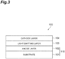
- Fig. 3 is a cross-sectional view of the organic EL element (organic electronic element) according to the embodiment.
- an organic EL element 100 of the embodiment has a configuration in which an anode layer 102, a light emitting layer (functional layer) 103, and a cathode layer 104 are sequentially laminated on a film-shaped substrate (substrate having flexibility or a flexible substrate) 101.
- a film-shaped substrate 101 for example, a transparent plastic, more specifically, PEN (Polyethylene Naphthalate) may be exemplified.
- PEN Polyethylene Naphthalate
- a substrate having a thickness of about 100 ⁇ m is typically exemplified.
- an electrode having light transmittance more specifically, a conductive metal oxide thin film formed of a relatively transparent material such as ITO (Tin-doped Indium Oxide) and IZO (Indium Zinc Oxide) is exemplified.
- the light emitting layer 103 includes various known organic EL materials such as a low-molecular-weight type material and a high-molecular-weight type material.
- an electrode having light reflectivity more specifically, a conductive metal thin film formed of a metal material is exemplified.
- a step (coating step) of forming the light emitting layer 103 on a film-shaped base material 110 including the substrate 101 and the anode layer 102 will be described and a known step of forming the anode layer 102 and the cathode layer 104 will be omitted.
- the anode layer 102 and the cathode layer 104 can be formed by, for example, a known method such as a vapor deposition method and a coating method for forming an electrode layer.
- the film base material 110 is horizontally conveyed by the roll-to-roll process. Specifically, the film base material 110 is unwound from the unwinding roller 10, and the film base material 110 is horizontally conveyed in the processing area A by the conveying rollers 11 and 12, and is wound by the winding roller 13.
- a conveying speed of the film base material 110 is set to, for example, be equal to or greater than 2 m/min and equal to or less than 6 m/min and a tension applied in the conveying direction of the film base material 110 is set to, for example, be equal to or larger than 20 N and equal to or smaller than 150 N and desirably equal to or larger than 30 N and equal to or smaller than 100 N.
- the tension (tensile force) applied in the conveying direction of the film base material 110 may be adjusted by a tension adjusting mechanism (not shown).
- the film base material 110 is floated by air using three air floating stages 20 disposed below the film base material 110.
- Each of the air floating stages 20 is formed of porous carbon and blows air from a plurality of minute holes.
- a width Wa of a top surface facing the film base material 110 in the air floating stage 20 is about 100 mm and a length La thereof is about 500 mm.
- the air floating stages 20 are arranged in the conveying direction at an interval Sa of 100 mm.
- the PEN film base material 110 having a thickness of 125 ⁇ m and a width Wf of 320 mm is assumed and an air blowing flow rate is set to be equal to or greater than 1 ⁇ 10 -4 L/(cm 2 ⁇ sec) and equal to or less than 3 ⁇ 10 -2 L/(cm 2 ⁇ sec) (air flow speed conversion which is equal to or greater than 0.001 m/sec and equal to or less than 0.3 m/sec) and desirably equal to or greater than 1 ⁇ 10 -4 L/(cm 2 ⁇ sec) and equal to or less than 1 ⁇ 10 -2 L/(cm 2 ⁇ sec).
- a gap between the air floating stage 20 and the film base material 110 is set to be equal to or larger than 30 ⁇ m and equal to or smaller than 1 mm and desirably equal to or larger than 50 ⁇ m and equal to or smaller than 500 ⁇ m.
- a vibration amount (highest position minus lowest position) of the film base material 110 is equal to or smaller than 70 ⁇ m and desirably equal to or smaller than 40 ⁇ m.
- a displacement amount of the film base material 110 is equal to or smaller than ⁇ 35 ⁇ m and desirably equal to or smaller than ⁇ 20 ⁇ m.
- the air floating stage 20 is not used to convey the film base material 110, but is used to float a part of the film base material 110 which droops due to its own weight. Thus, a relatively large amount of air produced by relatively large holes formed by processing is too strong. According to the air floating stage 20 of the embodiment, it is possible to float a part of the film base material 110 which droops due to its own weight by the use of a relatively small amount of air produced by relatively minute holes of the porous material.
- ink (coating solution) including an organic EL material is coated onto the film base material 110 by the slit coat applicator 30 disposed above the film base material 110 and the air floating stage 20 to form the light emitting layer 103.
- a layer having a thickness after drying of 20 nm to 100 nm is typically exemplified.
- the slit coat applicator 30 includes a slit which extends in a direction of the width Wf of the film base material 110.
- the ink relatively low-viscosity ink having a viscosity which is equal to or larger than 1 cP and equal to or smaller than 20 cP and desirably equal to or larger than 2 cP and equal to or smaller than 10 cP is used.
- a solution including an organic EL material and an organic solvent is used as the ink.
- the organic EL material a low-molecular-weight type material, a high-molecular-weight type material, or a mixture thereof may be used.
- the organic solvent may be any solvent as long as the solvent dissolves an organic EL material and is appropriately selected in consideration of the evaporation speed of the solvent, the surface tension and the viscosity of the solution, and the like.
- a single solvent or a mixed solvent may be used as the organic solvent.
- the film base material 110 is floated by air, it is possible to suppress the film base material 110 from drooping due to its own weight and to suppress the vertical vibration of the film base material 110.
- the film base material 110 is horizontally conveyed and the ink (coating solution) is coated onto the film base material 110 from above, it is possible to prevent dripping when the ink has low viscosity.
- the coating film (light emitting layer) 103 can be continuously and stably formed in the roll-to-roll process, the film thickness of the coating film is not uneven. As a result, it is possible to continuously manufacture a high-quality organic EL element (organic electronic element) having no uneven emission luminance (uneven light emission) with high throughput.
- a light emitting layer was formed in such a manner that an ink (coating solution) containing an organic EL material was coated onto a glass substrate instead of the film base material 110 using an inkjet applicator instead of the slit coat applicator 30.
- a polymer white light emitting material SCW 140 (having a solid content concentration of 7% and a viscosity of 5 cp) manufactured by Sumitomo Chemical Co., Ltd. was used as an ink and the thickness of the light emitting layer after drying was set to 70 nm.
- a vertical vibration was applied to the glass substrate when coating the ink thereon.
- uneven emission luminance uneven light emission
- the emission luminance was uneven at a vertical vibration amount (highest position minus lowest position) of 130 ⁇ m (displacement amount of ⁇ 65 ⁇ m) and the emission luminance was even at a vertical vibration amount of 70 ⁇ m (displacement amount of ⁇ 35 ⁇ m) and a vertical vibration amount of 40 ⁇ m ( ⁇ 20 ⁇ m).
- uneven emission luminance is reduced, that is, unevenness in film thickness of the light emitting layer (coating film) is reduced at a vertical vibration amount of 70 ⁇ m or less, more desirably 40 ⁇ m or less, in other words, a vertical displacement amount of ⁇ 35 ⁇ m or less, more desirably ⁇ 20 ⁇ m or less.
- the PEN film base material 110 having a thickness of 125 ⁇ m and a width Wf of 320 mm was horizontally conveyed.
- comparison verification was performed between a case of performing the air floating using the air floating stage 20 and a case of not performing the air floating.
- the verification conditions in the case of performing the air floating were as below.
- the vertical displacement amount of the film base material 110 was measured by measuring the vertical position of the film base material 110 at intervals of 1 msec for 20 seconds using a laser displacement sensor instead of the slit coat applicator 30. Verification results are shown in Fig. 4 .
- the vertical vibration amount (highest position minus lowest position) was 315 ⁇ m as shown in a curve 51.
- the vertical vibration amount was reduced to 17 ⁇ m as shown in a curve 50.
- the invention is not limited to the above-described embodiment and can be modified into various forms.
- a step of coating the light emitting layer of the organic EL element including the light emitting layer (functional layer) between a pair of electrodes has been exemplified.
- features of the invention can also be applied to steps of coating functional layers containing various organic materials, such as a hole injection layer, a hole transport layer, an electron transport layer, and an electron injection layer of various organic EL elements below.
- the sign "/" indicates a state where layers which are adjacent to each other with the sign "/" interposed therebetween are laminated on each other.
- the ink (coating solution) containing the organic EL material for the light emitting layer in the step of coating the light emitting layer may be replaced by the ink (coating solution) containing the organic material for the hole injection layer.
- the ink (coating solution) containing the organic EL material for the light emitting layer in the step of coating the light emitting layer may be replaced by the ink (coating solution) containing the organic material for the hole transport layer and further the film base material 110 may be replaced by the film base material including the substrate 101, the anode layer 102, and the hole injection layer 105.
- the film base material 110 may be replaced by the film base material including the substrate 101, the anode layer 102, the hole injection layer 105, and the hole transport layer 106.
- the ink (coating solution) containing the organic EL material for the light emitting layer in the step of coating the light emitting layer may be replaced by the ink (coating solution) containing the organic material of the electron transport layer and further the film base material 110 may be replaced by the film base material including the substrate 101, the anode layer 102, the hole injection layer 105, the hole transport layer 106, and the light emitting layer 103.
- the ink (coating solution) containing the organic EL material for the light emitting layer in the step of coating the light emitting layer may be replaced by the ink (coating solution) containing the organic material of the electron injection layer and further the film base material 110 may be replaced by the film base material including the substrate 101, the anode layer 102, the hole injection layer 105, the hole transport layer 106, the light emitting layer 103, and the electron transport layer 107.
- a manufacturing method in which the anode layer is disposed on the substrate side relative to the light emitting layer and the cathode layer is disposed on the opposite side to the substrate relative to the light emitting layer has been exemplified.
- features of the invention can also be applied to a manufacturing method in which the cathode layer is disposed on the substrate side relative to the light emitting layer and the anode layer is disposed on the opposite side to the substrate relative to the light emitting layer.
- a method for manufacturing the organic EL element has been exemplified.
- features of the invention can also be applied to a method for manufacturing an organic solar cell (organic electronic element) or an organic transistor (organic electronic element).
- features of the invention can also be applied to a step of forming an active layer (photoelectric conversion layer), a hole injection layer, a hole transport layer, an electron transport layer, and an electron injection layer in the method for manufacturing an organic solar cell.
- features of the invention can be also applied to a step of forming a semiconductor layer and an insulating layer in the method for manufacturing an organic transistor.
- a barrier layer is formed on any one of or both surfaces of the film base material.
- porous carbon has been exemplified as the material of the air floating stage, but various porous materials capable of blowing air can be employed.
- various conditions such as the air blowing flow rate, the number, the size, and the intervals of the air floating stages, the gap between the air floating stage and the film base material, and the tension applied in the conveying direction of the film base material have been exemplified.
- these conditions are set by assuming a PEN film base material having a thickness of 125 ⁇ m and a width of 320 mm.
- these conditions may be appropriately changed so that the vertical vibration amount of the film base material becomes equal to or smaller than 70 ⁇ m, in other words, the vertical displacement amount becomes equal to or smaller than ⁇ 35 ⁇ m.
Landscapes
- Engineering & Computer Science (AREA)
- Manufacturing & Machinery (AREA)
- Physics & Mathematics (AREA)
- Electromagnetism (AREA)
- Optics & Photonics (AREA)
- Electroluminescent Light Sources (AREA)
- Thin Film Transistor (AREA)
- Photovoltaic Devices (AREA)
Abstract
Description
- The present invention relates to a method for manufacturing an organic electronic element such as an organic EL element, an organic solar cell, and an organic transistor.
- An organic electronic element such as an organic EL (Electro Luminescence) element, an organic solar cell, and an organic transistor is known. Such an organic electronic element includes various functional layers such as a light emitting layer, a hole injection layer, a hole transport layer, an electron transport layer, an electron injection layer, an active layer, a semiconductor layer, and an insulating layer containing an organic material. Such an organic electronic element is formed on a film-shaped substrate (a substrate having flexibility or a flexible substrate) and is formed in a film shape.
- As a method for manufacturing the film-shaped organic electronic element, a method for forming various functional layers by a coating method such as an inkjet coating method and a die coater coating method using a roll-to-roll process is known.
Non-Patent Literature 1 discloses a die coater coating method (a slit coat coating method). - A case of forming the functional layer in the organic electronic element using the slit coat coating method will be described with reference to
Fig. 6 . In the slit coat coating method shown inFig. 6 , a film-shaped base material including a substrate is conveyed by a roll-to-roll structure including anunwinding roller 10 and awinding roller 13 andconveying rollers slit coat applicator 30X, thereby forming a functional layer thin film. At that time, the base material is fixed and stabilized by using abackup roller 15 in order to stabilize an underlying base material. - Fixing and stabilizing an underlying base material by using an adsorption stage instead of the
backup roller 15 are also known. - [Non-Patent Literature 1] Techno Smart Co., Ltd., Multi-layer Die Coater, [online], [Accessed on November 17, 2014], the Internet <URL:http://www.ctiweb.co.jp/soran/products/410>
- The slit coat coating method disclosed in Non-Patent
Literature 1 is suitable for a case in which a coating solution having high viscosity is used. Incidentally, there is a case in which a coating solution having low viscosity is used to form a thinner film. However, when the coating solution having low viscosity is used in the slit coat coating method disclosed in Non-PatentLiterature 1, dripping occurs. - When the backup roller is used as in the slit coat coating method disclosed in Non-Patent
Literature 1, a film thickness becomes uneven due to a mechanical vibration of the backup roller. Meanwhile, since the base material is temporarily adsorbed when the adsorption stage is used, the base material is conveyed intermittently and thus productivity is degraded. - Regarding the dripping, a case in which the base material is horizontally conveyed and a coating solution is coated onto a top surface of the base material by a coater disposed above the base material may be conceived. Regarding the mechanical vibration and the intermittent conveying, a case in which the backup roller and the adsorption stage are not used may be conceived. For example, the substrate may be horizontally conveyed by two conveying rollers separated from each other by a predetermined distance, and a coating solution may be coated onto the top surface of the base material from above between two conveying rollers without using the backup roller and the adsorption stage.
- However, in a configuration in which the backup roller and the adsorption stage are not used for the horizontal conveying in the case of the film-shaped base material, the base material droops due to its own weight between two conveying rollers and thus the base material is vibrated up and down. Due to this vibration, the film thickness of the coating film becomes uneven.
- Here, the invention is to provide a method for manufacturing an organic electronic element capable of reducing unevenness in thickness of a coating film.
- A method for manufacturing an organic electronic element of the invention is a method for manufacturing an organic electronic element including a functional layer containing an organic material, including a coating step of forming the functional layer by horizontally conveying a base material having flexibility using a roll-to-roll process and coating a coating solution containing the organic material onto the base material using a slit coat applicator disposed above the base material, wherein in the coating step, the base material is made to float on air using an air floating stage disposed below the base material and the coating solution is coated onto the base material. The coating step can be applied to form various functional layers such as a light emitting layer, a hole injection layer, a hole transport layer, an electron transport layer, an electron injection layer, an active layer, a semiconductor layer, and an insulating layer containing an organic material in an organic electronic element such as an organic EL element, an organic solar cell, and an organic transistor.
- According to the method for manufacturing an organic electronic element, since the base material is made to float on air, it is possible to suppress drooping of the base material due to its the own weight and to suppress vertical vibration of the base material. Thus, it is possible to reduce unevenness in film thickness of the coating film caused by the vertical vibration of the base material.
- According to the method for manufacturing the organic electronic element, since the base material is horizontally conveyed and the coating solution is coated onto the base material from above, it is possible to prevent dripping when the coating solution has a low viscosity.
- According to the method for manufacturing the organic electronic element, since the coating film (functional layer) can be continuously and stably formed in the roll-to-roll process, it is possible to continuously manufacture a high-quality organic electronic element having no unevenness in film thickness of the coating film with high throughput.
- The air floating stage may be formed of a porous material. The air floating stage is not used to convey the base material, but is used to float a part of the base material which droops due to its own weight. A relatively large amount of air produced by relatively large holes formed by processing is thus too strong. However, according to the embodiment, it is possible to float a part of the base material which droops due to its own weight by the use of a relatively small amount of air produced by the relatively small holes of the porous material.
- A vertical vibration amount (displacement amount) of the base material may be equal to or smaller than 70 µm (±35 µm). According to this embodiment, since the vertical vibration amount of the base material is as small as equal to or smaller than 70 µm (displacement amount of ±35 µm), it is possible to reduce unevenness in film thickness of the coating film caused by the vertical vibration of the base material.
- A gap between the air floating stage and the base material may be equal to or larger than 30 µm and equal to or smaller than 1 mm. According to this embodiment, it is possible to appropriately suppress the vertical vibration of the film caused by the blowing air between the air floating stage and the base material. When the gap is smaller than 30 µm, there is a concern that the back surface of the base material may be damaged due to contact between the air floating stage and the base material. In contrast, when the gap is larger than 1 mm, an air layer between the air floating stage and the base material becomes uneven and thus an effect of suppressing the vertical vibration becomes small.
- The viscosity of the coating solution may be equal to or larger than 1 cp and equal to or smaller than 20 cp. According to this embodiment, even with a low-viscosity coating solution of equal to or larger than 1 cp and equal to or smaller than 20 cp, it is possible to reduce unevenness in film thickness of the coating film caused by the vertical vibration of the base material. Further, dripping can be prevented as described above.
- A tensile force (tension) of the base material may be equal to or larger than 20 N and equal to or smaller than 150 N. According to this embodiment, since wrinkles and slack in the conveying direction do not occur in the film itself conveyed to enter the air floating stage, it is possible to form a stable and uniform coating film while suppressing a vertical vibration.
- An air flow speed of the air floating stage may be equal to or greater than 0.001 m/sec and equal to or less than 0.3 m/sec. As described above, the air floating stage is not used to convey the base material, but is used to float a part of the base material which droops due to its own weight. Thus, a relatively large amount of air produced by relatively large holes formed by processing is too strong. However, according to this configuration, since the air flow speed is as low as equal to or greater than 0.001 m/sec and equal to or less than 0.3 m/sec, it is possible to float a part of the base material which droops due to its own weight in the base material.
- The organic electronic element may be an organic EL element. According to this embodiment, it is possible to reduce uneven emission luminance (uneven light emission).
- The organic electronic element may be an organic solar cell. According to this embodiment, it is possible to select a material in a wide viscosity range for a coating process of an organic semiconductor material or an electrode material formed of metallic nano-particles.
- The organic electronic element may be an organic transistor. According to this embodiment, it is possible to select a wide range of materials without considering the viscosity range when an organic semiconductor material for an organic transistor, a material for a gate insulating film, and a printing material formed of metallic nano particles for source/drain electrodes are used.
- According to the invention, it is possible to reduce unevenness in film thickness of a coating film in an organic electronic element such as an organic EL element, an organic solar cell, and an organic transistor.
-
-
Fig. 1 is a diagram showing a method for manufacturing an organic EL element (organic electronic element) according to an embodiment of the invention. -
Fig. 2 is a diagram showing a processing area A shown inFig. 1 when viewed from above. -
Fig. 3 is a cross-sectional view of the organic EL element (organic electronic element) according to the embodiment. -
Fig. 4 is a diagram showing verification results. -
Fig. 5 is a cross-sectional view of an organic EL element (organic electronic element) according to a modified example. -
Fig. 6 is a diagram showing a method for manufacturing an organic EL element (organic electronic element) of the related art. - Hereinafter, a preferred embodiment of the invention will be described in detail with reference to the drawings. In the drawings, the same reference numerals will be given to the same or equivalent parts.
-
Fig. 1 is a diagram showing a method for manufacturing an organic EL element (organic electronic element) according to an embodiment of the invention andFig. 2 is a diagram showing a processing area A shown inFig. 1 when viewed from above.Fig. 3 is a cross-sectional view of the organic EL element (organic electronic element) according to the embodiment. - As shown in
Fig. 3 , anorganic EL element 100 of the embodiment has a configuration in which ananode layer 102, a light emitting layer (functional layer) 103, and acathode layer 104 are sequentially laminated on a film-shaped substrate (substrate having flexibility or a flexible substrate) 101. As a material of the film-shapedsubstrate 101, for example, a transparent plastic, more specifically, PEN (Polyethylene Naphthalate) may be exemplified. For the film-shapedsubstrate 101, a substrate having a thickness of about 100 µm is typically exemplified. As theanode layer 102, for example, an electrode having light transmittance, more specifically, a conductive metal oxide thin film formed of a relatively transparent material such as ITO (Tin-doped Indium Oxide) and IZO (Indium Zinc Oxide) is exemplified. Thelight emitting layer 103 includes various known organic EL materials such as a low-molecular-weight type material and a high-molecular-weight type material. As thecathode layer 104, for example, an electrode having light reflectivity, more specifically, a conductive metal thin film formed of a metal material is exemplified. - In a method for manufacturing an organic EL element shown below, a step (coating step) of forming the
light emitting layer 103 on a film-shapedbase material 110 including thesubstrate 101 and theanode layer 102 will be described and a known step of forming theanode layer 102 and thecathode layer 104 will be omitted. Theanode layer 102 and thecathode layer 104 can be formed by, for example, a known method such as a vapor deposition method and a coating method for forming an electrode layer. - First, as shown in
Figs. 1 and2 , thefilm base material 110 is horizontally conveyed by the roll-to-roll process. Specifically, thefilm base material 110 is unwound from the unwindingroller 10, and thefilm base material 110 is horizontally conveyed in the processing area A by the conveyingrollers roller 13. - For example, on the assumption of the PEN
film base material 110 having a thickness of 125 µm and a width Wf of 320 mm, a conveying speed of thefilm base material 110 is set to, for example, be equal to or greater than 2 m/min and equal to or less than 6 m/min and a tension applied in the conveying direction of thefilm base material 110 is set to, for example, be equal to or larger than 20 N and equal to or smaller than 150 N and desirably equal to or larger than 30 N and equal to or smaller than 100 N. The tension (tensile force) applied in the conveying direction of thefilm base material 110 may be adjusted by a tension adjusting mechanism (not shown). - In the processing area A in which the
film base material 110 is horizontally conveyed, thefilm base material 110 is floated by air using threeair floating stages 20 disposed below thefilm base material 110. Each of theair floating stages 20 is formed of porous carbon and blows air from a plurality of minute holes. For example, a width Wa of a top surface facing thefilm base material 110 in theair floating stage 20 is about 100 mm and a length La thereof is about 500 mm. Theair floating stages 20 are arranged in the conveying direction at an interval Sa of 100 mm. - For example, the PEN
film base material 110 having a thickness of 125 µm and a width Wf of 320 mm is assumed and an air blowing flow rate is set to be equal to or greater than 1×10⁻⁴ L/(cm2·sec) and equal to or less than 3×10⁻² L/(cm2·sec) (air flow speed conversion which is equal to or greater than 0.001 m/sec and equal to or less than 0.3 m/sec) and desirably equal to or greater than 1×10⁻⁴L/(cm2·sec) and equal to or less than 1×10⁻²L/(cm2·sec). - Accordingly, a gap between the
air floating stage 20 and thefilm base material 110 is set to be equal to or larger than 30 µm and equal to or smaller than 1 mm and desirably equal to or larger than 50 µm and equal to or smaller than 500 µm. As a result, a vibration amount (highest position minus lowest position) of thefilm base material 110 is equal to or smaller than 70 µm and desirably equal to or smaller than 40 µm. In other words, a displacement amount of thefilm base material 110 is equal to or smaller than ±35 µm and desirably equal to or smaller than ±20 µm. - The
air floating stage 20 is not used to convey thefilm base material 110, but is used to float a part of thefilm base material 110 which droops due to its own weight. Thus, a relatively large amount of air produced by relatively large holes formed by processing is too strong. According to theair floating stage 20 of the embodiment, it is possible to float a part of thefilm base material 110 which droops due to its own weight by the use of a relatively small amount of air produced by relatively minute holes of the porous material. - In the case of a relatively large amount of air produced by relatively large holes formed by processing, there is a case in which ink of a nozzle of a
slit coat applicator 30 to be described later may dry. However, in the case of a relatively small amount of air produced by relatively small holes of the porous material of the embodiment, such a problem does not arise. - In the processing area A in which the
film base material 110 is horizontally conveyed, ink (coating solution) including an organic EL material is coated onto thefilm base material 110 by theslit coat applicator 30 disposed above thefilm base material 110 and theair floating stage 20 to form thelight emitting layer 103. For thelight emitting layer 103, a layer having a thickness after drying of 20 nm to 100 nm (for example, a coating thickness of 0.4 µm to 2 µm) is typically exemplified. - The
slit coat applicator 30 includes a slit which extends in a direction of the width Wf of thefilm base material 110. - As the ink, relatively low-viscosity ink having a viscosity which is equal to or larger than 1 cP and equal to or smaller than 20 cP and desirably equal to or larger than 2 cP and equal to or smaller than 10 cP is used. For example, a solution including an organic EL material and an organic solvent is used as the ink. As the organic EL material, a low-molecular-weight type material, a high-molecular-weight type material, or a mixture thereof may be used. The organic solvent may be any solvent as long as the solvent dissolves an organic EL material and is appropriately selected in consideration of the evaporation speed of the solvent, the surface tension and the viscosity of the solution, and the like. As the organic solvent, a single solvent or a mixed solvent may be used.
- According to the method for manufacturing the organic EL element (organic electronic element) of the embodiment, since the
film base material 110 is floated by air, it is possible to suppress thefilm base material 110 from drooping due to its own weight and to suppress the vertical vibration of thefilm base material 110. Thus, it is possible to reduce unevenness in film thickness of the light emitting layer (coating film) caused by the vertical vibration of thefilm base material 110. As a result, it is possible to reduce uneven light emission luminance (uneven light emission). - According to the method for manufacturing the organic EL element (organic electronic element) of the embodiment, since the
film base material 110 is horizontally conveyed and the ink (coating solution) is coated onto thefilm base material 110 from above, it is possible to prevent dripping when the ink has low viscosity. - Further, according to the method for manufacturing the organic EL element (organic electronic element) of the embodiment, since the coating film (light emitting layer) 103 can be continuously and stably formed in the roll-to-roll process, the film thickness of the coating film is not uneven. As a result, it is possible to continuously manufacture a high-quality organic EL element (organic electronic element) having no uneven emission luminance (uneven light emission) with high throughput.
- Hereinafter, the above-described effect will be verified.
- A light emitting layer was formed in such a manner that an ink (coating solution) containing an organic EL material was coated onto a glass substrate instead of the
film base material 110 using an inkjet applicator instead of theslit coat applicator 30. A polymer white light emitting material SCW 140 (having a solid content concentration of 7% and a viscosity of 5 cp) manufactured by Sumitomo Chemical Co., Ltd. was used as an ink and the thickness of the light emitting layer after drying was set to 70 nm. A vertical vibration was applied to the glass substrate when coating the ink thereon. In the present verification, uneven emission luminance (uneven light emission) was visually checked for by irradiating UV rays from an UV lamp to the light emitting layer. - According to this verification, the emission luminance was uneven at a vertical vibration amount (highest position minus lowest position) of 130 µm (displacement amount of ±65 µm) and the emission luminance was even at a vertical vibration amount of 70 µm (displacement amount of ±35 µm) and a vertical vibration amount of 40 µm (±20 µm). From this, it could be understood that uneven emission luminance is reduced, that is, unevenness in film thickness of the light emitting layer (coating film) is reduced at a vertical vibration amount of 70 µm or less, more desirably 40 µm or less, in other words, a vertical displacement amount of ±35 µm or less, more desirably ±20 µm or less.
- According to the manufacturing method shown in
Figs. 1 and2 , the PENfilm base material 110 having a thickness of 125 µm and a width Wf of 320 mm was horizontally conveyed. At that time, comparison verification was performed between a case of performing the air floating using theair floating stage 20 and a case of not performing the air floating. The verification conditions in the case of performing the air floating were as below. - Air blowing flow rate: 3×10⁻⁴ L/(cm2·sec) (air flow speed conversion: 0.003 m/sec)
- Gap between
air floating stage 20 and film base material 110: 50 µm - Further, the other common verification conditions were as below.
- Conveying speed of film base material 110: 6 m/min
- Tension applied in conveying direction of film base material 110: 30 N
- In the present verification, the vertical displacement amount of the
film base material 110 was measured by measuring the vertical position of thefilm base material 110 at intervals of 1 msec for 20 seconds using a laser displacement sensor instead of theslit coat applicator 30. Verification results are shown inFig. 4 . - According to
Fig. 4 , in the case of not performing the air floating using theair floating stage 20, the vertical vibration amount (highest position minus lowest position) was 315 µm as shown in acurve 51. In contrast, in the case of performing the air floating using theair floating stage 20, the vertical vibration amount was reduced to 17 µm as shown in acurve 50. - From both the
verification 1 and theverification 2, it was verified that the uneven emission luminance could be reduced, that is, unevenness in film thickness of the light emitting layer (coating film) could be reduced by the air floating using theair floating stage 20. - The invention is not limited to the above-described embodiment and can be modified into various forms. For example, in the embodiment, a step of coating the light emitting layer of the organic EL element including the light emitting layer (functional layer) between a pair of electrodes has been exemplified. However, features of the invention can also be applied to steps of coating functional layers containing various organic materials, such as a hole injection layer, a hole transport layer, an electron transport layer, and an electron injection layer of various organic EL elements below.
- a) Anode/Light Emitting Layer/Cathode
- b) Anode/Hole Injection Layer/Light Emitting Layer/Cathode
- c) Anode/Hole Injection Layer/Light Emitting Layer/Electron Injection Layer/Cathode
- d) Anode/Hole Injection Layer/Light Emitting Layer/Electron Transport Layer/Electron Injection Layer/Cathode
- e) Anode/Hole Injection Layer/Hole Transport Layer/Light Emitting Layer/Cathode
- f) Anode/Hole Injection Layer/Hole Transport Layer/Light Emitting Layer/Electron Injection Layer/Cathode
- g) Anode/Hole Injection Layer/Hole Transport Layer/Light Emitting Layer/Electron Transport Layer/Electron Injection Layer/Cathode
- h) Anode/Light Emitting Layer/Electron Injection Layer/Cathode
- i) Anode/Light Emitting Layer/Electron Transport Layer/Electron Injection Layer/Cathode
- Here, the sign "/" indicates a state where layers which are adjacent to each other with the sign "/" interposed therebetween are laminated on each other.
- For example, in a step of coating the
hole injection layer 105 shown inFig. 5 , the ink (coating solution) containing the organic EL material for the light emitting layer in the step of coating the light emitting layer may be replaced by the ink (coating solution) containing the organic material for the hole injection layer. In a step of coating thehole transport layer 106 shown inFig. 5 , the ink (coating solution) containing the organic EL material for the light emitting layer in the step of coating the light emitting layer may be replaced by the ink (coating solution) containing the organic material for the hole transport layer and further thefilm base material 110 may be replaced by the film base material including thesubstrate 101, theanode layer 102, and thehole injection layer 105. In a step of coating thelight emitting layer 103 shown inFig. 5 , thefilm base material 110 may be replaced by the film base material including thesubstrate 101, theanode layer 102, thehole injection layer 105, and thehole transport layer 106. In a step of coating theelectron transport layer 107 shown inFig. 5 , the ink (coating solution) containing the organic EL material for the light emitting layer in the step of coating the light emitting layer may be replaced by the ink (coating solution) containing the organic material of the electron transport layer and further thefilm base material 110 may be replaced by the film base material including thesubstrate 101, theanode layer 102, thehole injection layer 105, thehole transport layer 106, and thelight emitting layer 103. In a step of coating theelectron injection layer 108 shown inFig. 5 , the ink (coating solution) containing the organic EL material for the light emitting layer in the step of coating the light emitting layer may be replaced by the ink (coating solution) containing the organic material of the electron injection layer and further thefilm base material 110 may be replaced by the film base material including thesubstrate 101, theanode layer 102, thehole injection layer 105, thehole transport layer 106, thelight emitting layer 103, and theelectron transport layer 107. - In the embodiment, as a method for manufacturing the organic EL element, a manufacturing method in which the anode layer is disposed on the substrate side relative to the light emitting layer and the cathode layer is disposed on the opposite side to the substrate relative to the light emitting layer has been exemplified. However, features of the invention can also be applied to a manufacturing method in which the cathode layer is disposed on the substrate side relative to the light emitting layer and the anode layer is disposed on the opposite side to the substrate relative to the light emitting layer.
- In the embodiment, a method for manufacturing the organic EL element (organic electronic element) has been exemplified. However, features of the invention can also be applied to a method for manufacturing an organic solar cell (organic electronic element) or an organic transistor (organic electronic element). For example, features of the invention can also be applied to a step of forming an active layer (photoelectric conversion layer), a hole injection layer, a hole transport layer, an electron transport layer, and an electron injection layer in the method for manufacturing an organic solar cell. Features of the invention can be also applied to a step of forming a semiconductor layer and an insulating layer in the method for manufacturing an organic transistor.
- Features of the invention can be also applied to a manufacturing method in which a barrier layer is formed on any one of or both surfaces of the film base material.
- In the embodiment, porous carbon has been exemplified as the material of the air floating stage, but various porous materials capable of blowing air can be employed.
- In the embodiment, various conditions such as the air blowing flow rate, the number, the size, and the intervals of the air floating stages, the gap between the air floating stage and the film base material, and the tension applied in the conveying direction of the film base material have been exemplified. However, these conditions are set by assuming a PEN film base material having a thickness of 125 µm and a width of 320 mm. When at least one of the size and the material of the film base material is greatly changed, these conditions may be appropriately changed so that the vertical vibration amount of the film base material becomes equal to or smaller than 70 µm, in other words, the vertical displacement amount becomes equal to or smaller than ±35 µm.
-
- 10 Unwinding roller
- 11, 12, 14 Conveying roller
- 13 Winding roller
- 15 Backup roller (conveying roller)
- 20 Air floating stage
- 30, 30X Slit coat applicator
- 100 Organic EL element (organic electronic element)
- 101 Substrate
- 102 Anode layer
- 103 Light emitting layer
- 104 Cathode layer
- 105 Hole injection layer
- 106 Hole transport layer
- 107 Electron transport layer
- 108 Electron injection layer
- 110 Film base material (base material).
Claims (10)
- A method for manufacturing an organic electronic element including a functional layer containing an organic material, comprising:a coating step of forming the functional layer by horizontally conveying a base material having flexibility using a roll-to-roll process and coating a coating solution containing the organic material onto the base material using a slit coat applicator disposed above the base material,wherein in the coating step, the base material is floated by air using an air floating stage disposed below the base material and the coating solution is coated onto the base material.
- The method for manufacturing the organic electronic element according to claim 1,
wherein the air floating stage is formed of a porous material. - The method for manufacturing the organic electronic element according to claim 1 or 2,
wherein a vertical vibration amount of the base material is equal to or smaller than 70 µm. - The method for manufacturing the organic electronic element according to claim 3,
wherein a gap between the air floating stage and the base material is equal to or larger than 30 µm and equal to or smaller than 1 mm. - The method for manufacturing the organic electronic element according to claim 3,
wherein a viscosity of the coating solution is equal to or larger than 1 cp and equal to or smaller than 20 cp. - The method for manufacturing the organic electronic element according to claim 3,
wherein a tensile force of the base material is equal to or larger than 20 N and equal to or smaller than 150 N. - The method for manufacturing the organic electronic element according to claim 3,
wherein an air flow speed generated by the air floating stage is equal to or greater than 0.001 m/sec and equal to or less than 0.3 m/sec. - The method for manufacturing the organic electronic element according to any one of claims 1 to 7,
wherein the organic electronic element is an organic EL element. - The method for manufacturing the organic electronic element according to any one of claims 1 to 7,
wherein the organic electronic element is an organic solar cell. - The method for manufacturing the organic electronic element according to any one of claims 1 to 7,
wherein the organic electronic element is an organic transistor.
Applications Claiming Priority (2)
| Application Number | Priority Date | Filing Date | Title |
|---|---|---|---|
| JP2015001583A JP5799181B1 (en) | 2015-01-07 | 2015-01-07 | Method for manufacturing organic electronic device |
| PCT/JP2015/085555 WO2016111144A1 (en) | 2015-01-07 | 2015-12-18 | Method for manufacturing organic electronic element |
Publications (2)
| Publication Number | Publication Date |
|---|---|
| EP3244701A1 true EP3244701A1 (en) | 2017-11-15 |
| EP3244701A4 EP3244701A4 (en) | 2018-10-03 |
Family
ID=54348664
Family Applications (1)
| Application Number | Title | Priority Date | Filing Date |
|---|---|---|---|
| EP15877017.2A Ceased EP3244701A4 (en) | 2015-01-07 | 2015-12-18 | Method for manufacturing organic electronic element |
Country Status (6)
| Country | Link |
|---|---|
| US (1) | US10319909B2 (en) |
| EP (1) | EP3244701A4 (en) |
| JP (1) | JP5799181B1 (en) |
| KR (1) | KR20170101980A (en) |
| CN (1) | CN107211501B (en) |
| WO (1) | WO2016111144A1 (en) |
Families Citing this family (5)
| Publication number | Priority date | Publication date | Assignee | Title |
|---|---|---|---|---|
| JP6254108B2 (en) | 2015-01-07 | 2017-12-27 | 住友化学株式会社 | Manufacturing method of organic EL panel |
| JP2017195115A (en) * | 2016-04-21 | 2017-10-26 | 住友化学株式会社 | Method for manufacturing organic EL device |
| KR102458991B1 (en) * | 2018-03-30 | 2022-10-25 | 제이에프이 스틸 가부시키가이샤 | Manufacturing method and continuous film forming apparatus for grain-oriented electrical steel sheet |
| KR102611146B1 (en) * | 2021-06-28 | 2023-12-06 | 세메스 주식회사 | Method for preheating substrate treating apparatus and computer program therefor |
| CN120857832A (en) * | 2025-07-21 | 2025-10-28 | 浙江大学 | Organic semiconductor single crystal thin film and its preparation method and use |
Family Cites Families (26)
| Publication number | Priority date | Publication date | Assignee | Title |
|---|---|---|---|---|
| JPS6436077U (en) * | 1987-08-28 | 1989-03-06 | ||
| US5136966A (en) | 1988-10-28 | 1992-08-11 | Konica Corporation | Web coating apparatus |
| JP2724400B2 (en) * | 1989-02-13 | 1998-03-09 | コニカ株式会社 | Web coating device |
| JP2724398B2 (en) * | 1989-02-13 | 1998-03-09 | コニカ株式会社 | Web coating device |
| JP4129861B2 (en) * | 2002-08-02 | 2008-08-06 | 大日本印刷株式会社 | Coating equipment |
| JP2004131215A (en) * | 2002-10-09 | 2004-04-30 | Ushio Inc | Conveyor for belt-like work |
| JP2004335492A (en) | 2003-03-07 | 2004-11-25 | Junji Kido | Coater of organic electronic material and process for producing organic electronic element using it |
| JP4767251B2 (en) * | 2004-04-14 | 2011-09-07 | コアフロー サイエンティフィック ソリューションズ リミテッド | A method for focusing an optical inspection apparatus on a contact surface of a flat object |
| US7966743B2 (en) | 2007-07-31 | 2011-06-28 | Eastman Kodak Company | Micro-structured drying for inkjet printers |
| KR101296659B1 (en) | 2008-11-14 | 2013-08-14 | 엘지디스플레이 주식회사 | Washing device |
| JP2010140705A (en) * | 2008-12-10 | 2010-06-24 | Konica Minolta Holdings Inc | Organic electroluminescent panel and manufacturing method therefor and lighting device and display using the organic electroluminescent panel |
| JP5418505B2 (en) * | 2009-02-03 | 2014-02-19 | コニカミノルタ株式会社 | Organic electronic device and method for manufacturing the same |
| JP5831228B2 (en) * | 2009-05-09 | 2015-12-09 | コニカミノルタ株式会社 | Application method |
| WO2012039218A1 (en) * | 2010-09-25 | 2012-03-29 | コニカミノルタホールディングス株式会社 | Coating method, and process for production of organic electronics element |
| JP2012192332A (en) | 2011-03-16 | 2012-10-11 | Toray Ind Inc | Coating apparatus, coating method, and method for manufacturing display member |
| WO2012172919A1 (en) * | 2011-06-14 | 2012-12-20 | コニカミノルタホールディングス株式会社 | Method for manufacturing organic electroluminescent element |
| KR20130003560A (en) * | 2011-06-30 | 2013-01-09 | 주식회사 에스에프에이 | Printer |
| JP2013016405A (en) * | 2011-07-06 | 2013-01-24 | Konica Minolta Holdings Inc | Organic electronic device and manufacturing method thereof |
| CN106919003B (en) | 2011-11-04 | 2018-10-16 | 株式会社尼康 | Pattern forming method and device, pattern exposure method and manufacturing method |
| JP5494899B2 (en) * | 2012-04-09 | 2014-05-21 | 三菱化学株式会社 | Composition for organic electroluminescent device and organic electroluminescent device |
| JP2014079708A (en) * | 2012-10-17 | 2014-05-08 | Tokyo Ohka Kogyo Co Ltd | Double-side coating device |
| JP6036249B2 (en) * | 2012-12-11 | 2016-11-30 | コニカミノルタ株式会社 | Method for manufacturing organic electroluminescence device |
| JP2014120350A (en) * | 2012-12-17 | 2014-06-30 | Konica Minolta Inc | Manufacturing method of organic electroluminescent element |
| JP6151053B2 (en) * | 2013-03-18 | 2017-06-21 | 東レ株式会社 | Coating apparatus, coating method, and display member manufacturing method |
| JP6312959B2 (en) * | 2013-07-17 | 2018-04-18 | セーレン株式会社 | Inkjet recording device |
| JP6254108B2 (en) | 2015-01-07 | 2017-12-27 | 住友化学株式会社 | Manufacturing method of organic EL panel |
-
2015
- 2015-01-07 JP JP2015001583A patent/JP5799181B1/en not_active Expired - Fee Related
- 2015-12-18 CN CN201580072619.6A patent/CN107211501B/en not_active Expired - Fee Related
- 2015-12-18 WO PCT/JP2015/085555 patent/WO2016111144A1/en not_active Ceased
- 2015-12-18 KR KR1020177021432A patent/KR20170101980A/en not_active Ceased
- 2015-12-18 EP EP15877017.2A patent/EP3244701A4/en not_active Ceased
- 2015-12-18 US US15/541,599 patent/US10319909B2/en not_active Expired - Fee Related
Also Published As
| Publication number | Publication date |
|---|---|
| US20180006222A1 (en) | 2018-01-04 |
| EP3244701A4 (en) | 2018-10-03 |
| JP5799181B1 (en) | 2015-10-21 |
| CN107211501B (en) | 2020-01-07 |
| WO2016111144A1 (en) | 2016-07-14 |
| JP2016126964A (en) | 2016-07-11 |
| US10319909B2 (en) | 2019-06-11 |
| KR20170101980A (en) | 2017-09-06 |
| CN107211501A (en) | 2017-09-26 |
Similar Documents
| Publication | Publication Date | Title |
|---|---|---|
| US10319909B2 (en) | Method for manufacturing organic electronic element | |
| JP5522170B2 (en) | Application method | |
| US20210359259A1 (en) | Display panel and display device | |
| JP5831228B2 (en) | Application method | |
| TW201448312A (en) | Organic electroluminescent device and method for manufacturing same | |
| US20180277781A1 (en) | Light-emitting device and display device | |
| US10686162B2 (en) | Method for manufacturing organic EL panel | |
| KR20150085604A (en) | organic light emitting diode and manufacturing method of the same | |
| JP5316415B2 (en) | Thin film forming method and organic electronics element | |
| JP2011131116A (en) | Coating method and organic electroluminescence element | |
| JP5677253B2 (en) | Film forming method and film forming apparatus | |
| JP5700043B2 (en) | Method for forming organic thin film layer, method for producing organic electroluminescence element | |
| JP5772826B2 (en) | Method for manufacturing organic electroluminescence element | |
| US10651430B2 (en) | Organic electronic element manufacturing method and organic electronic element | |
| JP6777477B2 (en) | Electric module manufacturing method and electric module manufacturing equipment | |
| JP6595894B2 (en) | Viscous material supply device and method for producing dye-sensitized solar cell | |
| JP6574563B2 (en) | Film manufacturing method and film conveying method for electronic member | |
| JP2018037556A (en) | Method for manufacturing electric module, and device for manufacturing electric module |
Legal Events
| Date | Code | Title | Description |
|---|---|---|---|
| STAA | Information on the status of an ep patent application or granted ep patent |
Free format text: STATUS: THE INTERNATIONAL PUBLICATION HAS BEEN MADE |
|
| PUAI | Public reference made under article 153(3) epc to a published international application that has entered the european phase |
Free format text: ORIGINAL CODE: 0009012 |
|
| STAA | Information on the status of an ep patent application or granted ep patent |
Free format text: STATUS: REQUEST FOR EXAMINATION WAS MADE |
|
| 17P | Request for examination filed |
Effective date: 20170707 |
|
| AK | Designated contracting states |
Kind code of ref document: A1 Designated state(s): AL AT BE BG CH CY CZ DE DK EE ES FI FR GB GR HR HU IE IS IT LI LT LU LV MC MK MT NL NO PL PT RO RS SE SI SK SM TR |
|
| AX | Request for extension of the european patent |
Extension state: BA ME |
|
| DAV | Request for validation of the european patent (deleted) | ||
| DAX | Request for extension of the european patent (deleted) | ||
| A4 | Supplementary search report drawn up and despatched |
Effective date: 20180903 |
|
| RIC1 | Information provided on ipc code assigned before grant |
Ipc: H01L 51/48 20060101ALI20180828BHEP Ipc: H01L 21/336 20060101ALI20180828BHEP Ipc: H01L 29/786 20060101ALI20180828BHEP Ipc: H01L 51/50 20060101ALI20180828BHEP Ipc: H01L 51/56 20060101ALI20180828BHEP Ipc: B05D 1/26 20060101ALI20180828BHEP Ipc: H05B 33/10 20060101AFI20180828BHEP |
|
| STAA | Information on the status of an ep patent application or granted ep patent |
Free format text: STATUS: EXAMINATION IS IN PROGRESS |
|
| 17Q | First examination report despatched |
Effective date: 20201016 |
|
| REG | Reference to a national code |
Ref country code: DE Ref legal event code: R003 |
|
| STAA | Information on the status of an ep patent application or granted ep patent |
Free format text: STATUS: THE APPLICATION HAS BEEN REFUSED |
|
| 18R | Application refused |
Effective date: 20211224 |