EP3244452A1 - Layout for device fabrication - Google Patents
Layout for device fabrication Download PDFInfo
- Publication number
- EP3244452A1 EP3244452A1 EP17161435.7A EP17161435A EP3244452A1 EP 3244452 A1 EP3244452 A1 EP 3244452A1 EP 17161435 A EP17161435 A EP 17161435A EP 3244452 A1 EP3244452 A1 EP 3244452A1
- Authority
- EP
- European Patent Office
- Prior art keywords
- trenches
- source
- gate
- forming
- lines
- Prior art date
- Legal status (The legal status is an assumption and is not a legal conclusion. Google has not performed a legal analysis and makes no representation as to the accuracy of the status listed.)
- Withdrawn
Links
Images


Classifications
-
- H—ELECTRICITY
- H10—SEMICONDUCTOR DEVICES; ELECTRIC SOLID-STATE DEVICES NOT OTHERWISE PROVIDED FOR
- H10D—INORGANIC ELECTRIC SEMICONDUCTOR DEVICES
- H10D12/00—Bipolar devices controlled by the field effect, e.g. insulated-gate bipolar transistors [IGBT]
- H10D12/211—Gated diodes
-
- H—ELECTRICITY
- H10—SEMICONDUCTOR DEVICES; ELECTRIC SOLID-STATE DEVICES NOT OTHERWISE PROVIDED FOR
- H10D—INORGANIC ELECTRIC SEMICONDUCTOR DEVICES
- H10D30/00—Field-effect transistors [FET]
- H10D30/60—Insulated-gate field-effect transistors [IGFET]
- H10D30/64—Double-diffused metal-oxide semiconductor [DMOS] FETs
- H10D30/66—Vertical DMOS [VDMOS] FETs
- H10D30/668—Vertical DMOS [VDMOS] FETs having trench gate electrodes, e.g. UMOS transistors
-
- H—ELECTRICITY
- H10—SEMICONDUCTOR DEVICES; ELECTRIC SOLID-STATE DEVICES NOT OTHERWISE PROVIDED FOR
- H10B—ELECTRONIC MEMORY DEVICES
- H10B43/00—EEPROM devices comprising charge-trapping gate insulators
- H10B43/20—EEPROM devices comprising charge-trapping gate insulators characterised by three-dimensional [3D] arrangements, e.g. with cells on different height levels
- H10B43/23—EEPROM devices comprising charge-trapping gate insulators characterised by three-dimensional [3D] arrangements, e.g. with cells on different height levels with source and drain on different levels, e.g. with sloping channels
- H10B43/27—EEPROM devices comprising charge-trapping gate insulators characterised by three-dimensional [3D] arrangements, e.g. with cells on different height levels with source and drain on different levels, e.g. with sloping channels the channels comprising vertical portions, e.g. U-shaped channels
-
- H—ELECTRICITY
- H10—SEMICONDUCTOR DEVICES; ELECTRIC SOLID-STATE DEVICES NOT OTHERWISE PROVIDED FOR
- H10D—INORGANIC ELECTRIC SEMICONDUCTOR DEVICES
- H10D1/00—Resistors, capacitors or inductors
-
- H—ELECTRICITY
- H10—SEMICONDUCTOR DEVICES; ELECTRIC SOLID-STATE DEVICES NOT OTHERWISE PROVIDED FOR
- H10D—INORGANIC ELECTRIC SEMICONDUCTOR DEVICES
- H10D12/00—Bipolar devices controlled by the field effect, e.g. insulated-gate bipolar transistors [IGBT]
- H10D12/01—Manufacture or treatment
- H10D12/021—Manufacture or treatment of gated diodes, e.g. field-controlled diodes [FCD]
-
- H—ELECTRICITY
- H10—SEMICONDUCTOR DEVICES; ELECTRIC SOLID-STATE DEVICES NOT OTHERWISE PROVIDED FOR
- H10D—INORGANIC ELECTRIC SEMICONDUCTOR DEVICES
- H10D30/00—Field-effect transistors [FET]
- H10D30/01—Manufacture or treatment
- H10D30/021—Manufacture or treatment of FETs having insulated gates [IGFET]
- H10D30/028—Manufacture or treatment of FETs having insulated gates [IGFET] of double-diffused metal oxide semiconductor [DMOS] FETs
- H10D30/0291—Manufacture or treatment of FETs having insulated gates [IGFET] of double-diffused metal oxide semiconductor [DMOS] FETs of vertical DMOS [VDMOS] FETs
- H10D30/0297—Manufacture or treatment of FETs having insulated gates [IGFET] of double-diffused metal oxide semiconductor [DMOS] FETs of vertical DMOS [VDMOS] FETs using recessing of the gate electrodes, e.g. to form trench gate electrodes
-
- H—ELECTRICITY
- H10—SEMICONDUCTOR DEVICES; ELECTRIC SOLID-STATE DEVICES NOT OTHERWISE PROVIDED FOR
- H10D—INORGANIC ELECTRIC SEMICONDUCTOR DEVICES
- H10D62/00—Semiconductor bodies, or regions thereof, of devices having potential barriers
- H10D62/10—Shapes, relative sizes or dispositions of the regions of the semiconductor bodies; Shapes of the semiconductor bodies
- H10D62/124—Shapes, relative sizes or dispositions of the regions of semiconductor bodies or of junctions between the regions
- H10D62/126—Top-view geometrical layouts of the regions or the junctions
- H10D62/127—Top-view geometrical layouts of the regions or the junctions of cellular field-effect devices, e.g. multicellular DMOS transistors or IGBTs
-
- H—ELECTRICITY
- H10—SEMICONDUCTOR DEVICES; ELECTRIC SOLID-STATE DEVICES NOT OTHERWISE PROVIDED FOR
- H10D—INORGANIC ELECTRIC SEMICONDUCTOR DEVICES
- H10D64/00—Electrodes of devices having potential barriers
- H10D64/111—Field plates
- H10D64/117—Recessed field plates, e.g. trench field plates or buried field plates
-
- H—ELECTRICITY
- H10—SEMICONDUCTOR DEVICES; ELECTRIC SOLID-STATE DEVICES NOT OTHERWISE PROVIDED FOR
- H10D—INORGANIC ELECTRIC SEMICONDUCTOR DEVICES
- H10D64/00—Electrodes of devices having potential barriers
- H10D64/20—Electrodes characterised by their shapes, relative sizes or dispositions
- H10D64/27—Electrodes not carrying the current to be rectified, amplified, oscillated or switched, e.g. gates
- H10D64/311—Gate electrodes for field-effect devices
- H10D64/411—Gate electrodes for field-effect devices for FETs
- H10D64/511—Gate electrodes for field-effect devices for FETs for IGFETs
- H10D64/512—Disposition of the gate electrodes, e.g. buried gates
- H10D64/513—Disposition of the gate electrodes, e.g. buried gates within recesses in the substrate, e.g. trench gates, groove gates or buried gates
-
- H—ELECTRICITY
- H10—SEMICONDUCTOR DEVICES; ELECTRIC SOLID-STATE DEVICES NOT OTHERWISE PROVIDED FOR
- H10D—INORGANIC ELECTRIC SEMICONDUCTOR DEVICES
- H10D62/00—Semiconductor bodies, or regions thereof, of devices having potential barriers
- H10D62/10—Shapes, relative sizes or dispositions of the regions of the semiconductor bodies; Shapes of the semiconductor bodies
- H10D62/13—Semiconductor regions connected to electrodes carrying current to be rectified, amplified or switched, e.g. source or drain regions
- H10D62/149—Source or drain regions of field-effect devices
- H10D62/151—Source or drain regions of field-effect devices of IGFETs
- H10D62/152—Source regions of DMOS transistors
- H10D62/154—Dispositions
-
- H—ELECTRICITY
- H10—SEMICONDUCTOR DEVICES; ELECTRIC SOLID-STATE DEVICES NOT OTHERWISE PROVIDED FOR
- H10D—INORGANIC ELECTRIC SEMICONDUCTOR DEVICES
- H10D64/00—Electrodes of devices having potential barriers
- H10D64/20—Electrodes characterised by their shapes, relative sizes or dispositions
- H10D64/27—Electrodes not carrying the current to be rectified, amplified, oscillated or switched, e.g. gates
- H10D64/311—Gate electrodes for field-effect devices
- H10D64/411—Gate electrodes for field-effect devices for FETs
- H10D64/511—Gate electrodes for field-effect devices for FETs for IGFETs
- H10D64/517—Gate electrodes for field-effect devices for FETs for IGFETs characterised by the conducting layers
- H10D64/519—Gate electrodes for field-effect devices for FETs for IGFETs characterised by the conducting layers characterised by their top-view geometrical layouts
Definitions
- Trench gate technology is commonly used for improved break down voltage characteristics in semiconductor devices, especially high voltage devices.
- the gate is vertically buried in the source, typically separated by an isolation cover.
- Other advantages of the trench gate technology include reduced junction gate field effect transistor (JFET) effect that may be undesirable at least in some applications.
- JFET junction gate field effect transistor
- the trench gate technology does offer some disadvantages when lower voltage configurations are desired due to a need to reduce the width of the embedded gate.
- a device in one embodiment, includes a semiconductor substrate, a plurality of source lines formed on a surface of the semiconductor substrate. The plurality of source lines are laid in both X and Y directions. The device further includes a plurality of gate lines laid out over source lines in X direction in the plurality of source lines, a source contact line that connects source lines in the plurality of source lines that are terminating in Y direction, a gate contact line that connects the plurality of gate lines and a drain contact.
- the surface of the semiconductor substrate includes an epitaxial layer wherein the top surface of the epitaxial layer includes a p-type body implant.
- N-type layers run along the source lines in the plurality of source lines in Y direction.
- the gate lines protrude the surface of the semiconductor surface.
- An isolation layer exists between the source layer and the gate layer. The isolation layer exists only in X direction. The distance between individual source lines in the plurality of source lines is user defined based for desired electrical characteristics of the device.
- a second isolation layer is buried in trenches to cover buried parts of the plurality of source lines.
- a process of manufacturing a device includes forming an epitaxial layer in top surface of a wafer, forming a body layer in top surface of the epitaxial layer, forming a plurality of source implant strips in Y direction only, forming an intersecting network of trenches including trenches in X and Y directions.
- the trenches in Y direction cuts through each of the plurality of source implant strips.
- the process further includes filling trenches in the intersecting network of trenches with a dielectric material, forming source trenches in the dielectric material, filling the source trenches with source polysilicon, forming gate trenches in the source trenches, and filling the gate trenches with gate polysilicon such that a part thereof protrude over the top surface of the wafer.
- isolation trenches are formed in the source trenches and filled with an isolation material.
- the process of forming the source trenches includes forming a source contact trench for forming a source contact strip.
- Forming the gate trenches includes forming a gate contact trench for forming a gate contact strip.
- FIG. 1 depicts a schematic of a section of a device showing an initial fabrication stage.
- a wafer 100 is doped with n-type implants.
- An epitaxial layer 102 of type n or n+ is implanted on the upper surface of the wafer 100. Note that the depth of various layers shown in figures are not drawn to scale.
- a p-type body region 104 is implanted on the upper surface of the epitaxial layer 102.
- N-type stripps 106 are then implanted in Y direction at regular interval pursuant to a desired source pitch, significant thereof to be discussed later in this document.
- Trenches are then etched in cross section pattern. Trenches in Y direction overlaps the n-type layers 106. For the ease of description, only on portion of the trench pattern is being shown. In practice, the trench network will appear as shown in the plan view in Figure 5 .
- a dielectric material deposited on the trench walls.
- the trenches are filled with a dielectric material 108. If the entire trench is filled with the dielectric material, a part of the dielectric material will need to be etched to create trenches for the source layer.
- the process for performing above steps e.g., implanting impurities, etching trenches, etc. is well known in the art.
- the thickness of the dielectric layer 108 is typically between 100nm and 600nm depending upon desired drain characteristics.
- the packaging includes forming metal contacts.
- the trench width may be 6 micron for a 100v device and 4.5 micron for a 50v device.
- FIG. 2 illustrates a source layer 110 deposited in trenches.
- the dielectric material 108 may be deposited on the walls of trenches described in Figure 1 .
- trenches are etched in the dielectric layer 108 when the first trenches are filled with the dielectric material 108. These new trenches have smaller width and depth than the width of the dielectric layer 108 such that a desired amount of dielectric is left between the trench wall and the body region layer 104 and the epitaxial layer 102.
- n-type polysilicon layer (source layer) 110 is deposited. After depositing the source layer 110, the chemical mechanical planarization (CMP) may be performed to make the top surface plain.
- CMP chemical mechanical planarization
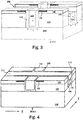
- FIG. 3 depicts a new set of trenches 109 in X direction.
- photoresist is deposited over the surface such that the source layer 110 and adjacent oxide dielectric layer 108 are exposed in X direction only.
- Etching is then performed to etch away the dielectric layer 108 and the source layer 110 in X direction to a desired depth, as shown, based on desired electrical characteristics of the device being formed.
- the gate oxidation process is performed to deposit a thin layer 113 ( Fig. 4 ) of dielectric on the bottom and walls of the trenches in X direction.
- the gate layer 112 is formed by depositing n-type polysilicon in these trenches.
- the CMP process may be performed after forming the gate layer 112.
- a top isolation layer and contacts (not shown) for the source, the drain and the gate may be formed.
- FIG. 5 depicts a top view of the device cut out from the wafer 100 showing gate 112 and source 110 lines and a gate contact 124 and a source contact 126.
- a trench for the source contact line 126 is formed together with the formation of the source layer 110 and the gate contact line 124 is formed with the trench in which the gate layer 112 is formed, as described in Fig. 3 .
- the source contact line 126 is used for attaching a source metal contact and the gate contact line 124 is used for attaching a gate metal contact.
- a drain contact is attached to the wafer 100. As depicted the source contact line 126 is connected to the gate layer 110 in Y direction and the gate contact line 124 connects the gate layer 112 in X direction. Even though not shown in Fig.
- the source layer 110 is also located under the gate layer 112. Further, as depicted, the source layer 110 comprises source lines laid out in both X and Y directions with the source lines in X direction intersects with the source lines in Y direction. The source lines in X direction are overlapped by the gate lines of the gate layer 112. In some embodiments, not all source lines in X direction may be overlapped by the gate lines.
- the gate pitch 120 and the source pitch 122 may be varied for changing electrical characteristics of the device. With this square layout scheme the breakdown voltage (BVdss) can be greatly enhanced.
- the dynamic performance of the device can be optimized as the gate pitch 120 can be greater than the source pitch 122. Therefore, the gate-drain charge (Q gd ) can be smaller than the gate-source charge (Q gs ). Having Q gd ⁇ Q gs improves gate bounce and spiking performance.
- the layout provided herein can be used to easily change the switching performance of a device depending upon a type of application simply by changing gate and source pitches.
- the dynamic performance can be improved due to a reduced density of gate polysilicon with a minimal impact of state resistance of the device (R dson ) because channel resistance is less than the distance between the top and bottom trenches (epitaxial resistance) for higher voltages.
Landscapes
- Electrodes Of Semiconductors (AREA)
- Engineering & Computer Science (AREA)
- General Engineering & Computer Science (AREA)
Abstract
A device is disclosed. The device includes a semiconductor substrate, a plurality of source lines formed on a surface of the semiconductor substrate as polysilicon layers formed in trenches having a dielectric layer at their bottom and walls. The plurality of source lines are laid in both X and Y directions. The device further includes a plurality of gate lines as polysilicon layers laid out over and insulated from the source lines in X direction in the plurality of source lines, a source contact line that connects source lines in the plurality of source lines that are terminating in Y direction, a gate contact line that connects the plurality of gate lines and a drain contact.
Description
- Trench gate technology is commonly used for improved break down voltage characteristics in semiconductor devices, especially high voltage devices. In the trench gate technology, the gate is vertically buried in the source, typically separated by an isolation cover. Other advantages of the trench gate technology include reduced junction gate field effect transistor (JFET) effect that may be undesirable at least in some applications. However, the trench gate technology does offer some disadvantages when lower voltage configurations are desired due to a need to reduce the width of the embedded gate.
- This Summary is provided to introduce a selection of concepts in a simplified form that are further described below in the Detailed Description. This Summary is not intended to identify key features or essential features of the claimed subject matter, nor is it intended to be used to limit the scope of the claimed subject matter.
- In one embodiment, a device is disclosed. The device includes a semiconductor substrate, a plurality of source lines formed on a surface of the semiconductor substrate. The plurality of source lines are laid in both X and Y directions. The device further includes a plurality of gate lines laid out over source lines in X direction in the plurality of source lines, a source contact line that connects source lines in the plurality of source lines that are terminating in Y direction, a gate contact line that connects the plurality of gate lines and a drain contact.
- In some embodiments, the surface of the semiconductor substrate includes an epitaxial layer wherein the top surface of the epitaxial layer includes a p-type body implant. N-type layers run along the source lines in the plurality of source lines in Y direction. The gate lines protrude the surface of the semiconductor surface. An isolation layer exists between the source layer and the gate layer. The isolation layer exists only in X direction. The distance between individual source lines in the plurality of source lines is user defined based for desired electrical characteristics of the device. A second isolation layer is buried in trenches to cover buried parts of the plurality of source lines.
- In another embodiment, a process of manufacturing a device is disclosed. The process includes forming an epitaxial layer in top surface of a wafer, forming a body layer in top surface of the epitaxial layer, forming a plurality of source implant strips in Y direction only, forming an intersecting network of trenches including trenches in X and Y directions. The trenches in Y direction cuts through each of the plurality of source implant strips. The process further includes filling trenches in the intersecting network of trenches with a dielectric material, forming source trenches in the dielectric material, filling the source trenches with source polysilicon, forming gate trenches in the source trenches, and filling the gate trenches with gate polysilicon such that a part thereof protrude over the top surface of the wafer.
- In some embodiments, prior to filling the gate trenches with gate polysilicon, isolation trenches are formed in the source trenches and filled with an isolation material. The process of forming the source trenches includes forming a source contact trench for forming a source contact strip. Forming the gate trenches includes forming a gate contact trench for forming a gate contact strip.
- So that the manner in which the above recited features of the present invention can be understood in detail, a more particular description of the invention, briefly summarized above, may be had by reference to embodiments, some of which are illustrated in the appended drawings. It is to be noted, however, that the appended drawings illustrate only typical embodiments of this invention and are therefore not to be considered limiting of its scope, for the invention may admit to other equally effective embodiments. Advantages of the subject matter claimed will become apparent to those skilled in the art upon reading this description in conjunction with the accompanying drawings, in which like reference numerals have been used to designate like elements, and in which:
-
FIG. 1 depicts a schematic of a section of a device showing an isolation material deposited in trenches in both X and Y directions in accordance with one or more embodiments of the present disclosure; -
FIG. 2 illustrates a source layer deposited in trenches in the isolation layer in accordance with one of more embodiments of the present disclosure; -
FIG. 3 depicts etched isolation and source layers in X direction in accordance with one or more embodiments of the present disclosure; -
FIG. 4 depicts the gate layer formed over the source layer in X direction in accordance with one of more embodiments of the present disclosure; and -
FIG. 5 depicts a top view of the device showing gate and source formations and gate and source contacts in accordance with one or more embodiments. - Note that figures are not drawn to scale. Intermediate steps between figure transitions have been omitted so as not to obfuscate the disclosure. Those intermediate steps are known to a person skilled in the art.
- It should be noted that the embodiments described herein use n-channel device for example only. A person skilled in the art would realize that these embodiments can also be applied for p-channel devices. Many well-known fabrication steps, components, and connectors have been omitted from the description so as not to obfuscate the present disclosure.
-
FIG. 1 depicts a schematic of a section of a device showing an initial fabrication stage. Awafer 100 is doped with n-type implants. Anepitaxial layer 102 of type n or n+ is implanted on the upper surface of thewafer 100. Note that the depth of various layers shown in figures are not drawn to scale. A p-type body region 104 is implanted on the upper surface of theepitaxial layer 102. N-type stripps 106 are then implanted in Y direction at regular interval pursuant to a desired source pitch, significant thereof to be discussed later in this document. - Trenches are then etched in cross section pattern. Trenches in Y direction overlaps the n-
type layers 106. For the ease of description, only on portion of the trench pattern is being shown. In practice, the trench network will appear as shown in the plan view inFigure 5 . In one embodiment a dielectric material deposited on the trench walls. In another embodiment, the trenches are filled with adielectric material 108. If the entire trench is filled with the dielectric material, a part of the dielectric material will need to be etched to create trenches for the source layer. As noted earlier, the process for performing above steps (e.g., implanting impurities, etching trenches, etc.) is well known in the art. If thedielectric material 108 is deposited on the walls of trenches or if a second set of trenches is etched after filling the first set of trenches with thedielectric material 108, the thickness of thedielectric layer 108 is typically between 100nm and 600nm depending upon desired drain characteristics. - It should be noted that patterns can be repeated on the
wafer 100 and after the process described herein is completed, individual discrete devices can be cut out and packaged. The packaging includes forming metal contacts. In some embodiments and for example only, the trench width may be 6 micron for a 100v device and 4.5 micron for a 50v device. -
FIG. 2 illustrates asource layer 110 deposited in trenches. As stated above, thedielectric material 108 may be deposited on the walls of trenches described inFigure 1 . Alternatively, trenches are etched in thedielectric layer 108 when the first trenches are filled with thedielectric material 108. These new trenches have smaller width and depth than the width of thedielectric layer 108 such that a desired amount of dielectric is left between the trench wall and thebody region layer 104 and theepitaxial layer 102. In these trenches, n-type polysilicon layer (source layer) 110 is deposited. After depositing thesource layer 110, the chemical mechanical planarization (CMP) may be performed to make the top surface plain. -
FIG. 3 depicts a new set oftrenches 109 in X direction. After the CMP process described above, photoresist is deposited over the surface such that thesource layer 110 and adjacentoxide dielectric layer 108 are exposed in X direction only. Etching is then performed to etch away thedielectric layer 108 and thesource layer 110 in X direction to a desired depth, as shown, based on desired electrical characteristics of the device being formed. After forming thesetrenches 109 in X direction only, the gate oxidation process is performed to deposit a thin layer 113 (Fig. 4 ) of dielectric on the bottom and walls of the trenches in X direction. - After depositing
dielectric layer 113 on the walls and bottom on these trenches in X direction over thesource layer 110, thegate layer 112 is formed by depositing n-type polysilicon in these trenches. The CMP process may be performed after forming thegate layer 112. Subsequently, a top isolation layer and contacts (not shown) for the source, the drain and the gate may be formed. -
FIG. 5 depicts a top view of the device cut out from thewafer 100showing gate 112 andsource 110 lines and agate contact 124 and asource contact 126. A trench for thesource contact line 126 is formed together with the formation of thesource layer 110 and thegate contact line 124 is formed with the trench in which thegate layer 112 is formed, as described inFig. 3 . Thesource contact line 126 is used for attaching a source metal contact and thegate contact line 124 is used for attaching a gate metal contact. A drain contact is attached to thewafer 100. As depicted thesource contact line 126 is connected to thegate layer 110 in Y direction and thegate contact line 124 connects thegate layer 112 in X direction. Even though not shown inFig. 5 , it should be noted that thesource layer 110 is also located under thegate layer 112. Further, as depicted, thesource layer 110 comprises source lines laid out in both X and Y directions with the source lines in X direction intersects with the source lines in Y direction. The source lines in X direction are overlapped by the gate lines of thegate layer 112. In some embodiments, not all source lines in X direction may be overlapped by the gate lines. - The
gate pitch 120 and thesource pitch 122 may be varied for changing electrical characteristics of the device. With this square layout scheme the breakdown voltage (BVdss) can be greatly enhanced. The dynamic performance of the device can be optimized as thegate pitch 120 can be greater than thesource pitch 122. Therefore, the gate-drain charge (Qgd) can be smaller than the gate-source charge (Qgs). Having Qgd <<< Qgs improves gate bounce and spiking performance. The layout provided herein can be used to easily change the switching performance of a device depending upon a type of application simply by changing gate and source pitches. The dynamic performance can be improved due to a reduced density of gate polysilicon with a minimal impact of state resistance of the device (Rdson) because channel resistance is less than the distance between the top and bottom trenches (epitaxial resistance) for higher voltages. - Some or all of these embodiments may be combined, some may be omitted altogether, and additional process steps can be added while still achieving the products described herein. Thus, the subject matter described herein can be embodied in many different variations, and all such variations are contemplated to be within the scope of what is claimed.
- While one or more implementations have been described by way of example and in terms of the specific embodiments, it is to be understood that one or more implementations are not limited to the disclosed embodiments. To the contrary, it is intended to cover various modifications and similar arrangements as would be apparent to those skilled in the art. Therefore, the scope of the appended claims should be accorded the broadest interpretation so as to encompass all such modifications and similar arrangements.
- The use of the terms "a" and "an" and "the" and similar referents in the context of describing the subject matter (particularly in the context of the following claims) are to be construed to cover both the singular and the plural, unless otherwise indicated herein or clearly contradicted by context. Recitation of ranges of values herein are merely intended to serve as a shorthand method of referring individually to each separate value falling within the range, unless otherwise indicated herein, and each separate value is incorporated into the specification as if it were individually recited herein. Furthermore, the foregoing description is for the purpose of illustration only, and not for the purpose of limitation, as the scope of protection sought is defined by the claims as set forth hereinafter together with any equivalents thereof entitled to. The use of any and all examples, or exemplary language (e.g., "such as") provided herein, is intended merely to better illustrate the subject matter and does not pose a limitation on the scope of the subject matter unless otherwise claimed. The use of the term "based on" and other like phrases indicating a condition for bringing about a result, both in the claims and in the written description, is not intended to foreclose any other conditions that bring about that result. No language in the specification should be construed as indicating any non-claimed element as essential to the practice of the invention as claimed.
- Preferred embodiments are described herein, including the best mode known to the inventor for carrying out the claimed subject matter. Of course, variations of those preferred embodiments will become apparent to those of ordinary skill in the art upon reading the foregoing description. The inventor expects skilled artisans to employ such variations as appropriate, and the inventor intends for the claimed subject matter to be practiced otherwise than as specifically described herein. Accordingly, this claimed subject matter includes all modifications and equivalents of the subject matter recited in the claims appended hereto as permitted by applicable law. Moreover, any combination of the above-described elements in all possible variations thereof is encompassed unless otherwise indicated herein or otherwise clearly contradicted by context.
Claims (13)
- A device comprising:a semiconductor substrate;a plurality of source lines formed on a surface of the semiconductor substrate, wherein the plurality of source lines are laid in both X and Y directions;a plurality of gate lines laid out over source lines in X direction in the plurality of source lines;a source contact line that connects source lines in the plurality of source lines that are terminating in Y direction;a gate contact line that connects the plurality of gate lines; anda drain contact.
- The device of claim 1, wherein the surface of the semiconductor substrate includes an epitaxial layer.
- The device of claim 2, wherein a top surface of the epitaxial layer includes a p-type body implant.
- The device of any preceding claim, wherein n-type layers run along the source lines in the plurality of source lines in Y direction.
- The device of any preceding claim, wherein the gate lines protrude the surface of the semiconductor surface.
- The device of any preceding claim, further including an isolation layer between the source layer and the gate layer.
- The device of claim 6, wherein the isolation layer exists only in X direction.
- The device of any preceding claim, wherein a distance between individual source lines in the plurality of source lines is user defined based for desired electrical characteristics of the device.
- The device of any preceding claim, further includes an isolation layer buried in trenches to cover buried parts of the plurality of source lines.
- A process of manufacturing a device, the process comprising:forming an epitaxial layer in top surface of a wafer;forming a body layer in top surface of the epitaxial layer;forming a plurality of source implant strips in Y direction only;forming an intersecting network of trenches including trenches in X and Y directions, wherein the trenches in Y direction cuts through each of the plurality of source implant strips;depositing a dielectric material on walls of trenches in the intersecting network of trenches;filling the trenches in the intersecting network of trenches with source polysilicon;forming gate trenches in the source trenches in X direction only; andfilling the gate trenches with gate polysilicon such that a part thereof protrude over the top surface of the wafer.
- The process of claim 10, wherein prior to filling the gate trenches with gate polysilicon, depositing a dielectric material on walls of the gate trenches.
- The process of any of claims 10 to 11, wherein the forming source trenches includes forming a source contact trench for forming a source contact strip.
- The process of any of claims 10 to 12, wherein the forming gate trenches includes forming a gate contact trench for forming a gate contact strip.
Applications Claiming Priority (1)
| Application Number | Priority Date | Filing Date | Title |
|---|---|---|---|
| US15/150,225 US9570605B1 (en) | 2016-05-09 | 2016-05-09 | Semiconductor device having a plurality of source lines being laid in both X and Y directions |
Publications (1)
| Publication Number | Publication Date |
|---|---|
| EP3244452A1 true EP3244452A1 (en) | 2017-11-15 |
Family
ID=57964989
Family Applications (1)
| Application Number | Title | Priority Date | Filing Date |
|---|---|---|---|
| EP17161435.7A Withdrawn EP3244452A1 (en) | 2016-05-09 | 2017-03-16 | Layout for device fabrication |
Country Status (3)
| Country | Link |
|---|---|
| US (1) | US9570605B1 (en) |
| EP (1) | EP3244452A1 (en) |
| CN (1) | CN107452789B (en) |
Cited By (1)
| Publication number | Priority date | Publication date | Assignee | Title |
|---|---|---|---|---|
| EP3817067A1 (en) * | 2019-10-30 | 2021-05-05 | Nexperia B.V. | Combined mcd and mos transistor semiconductor device |
Families Citing this family (3)
| Publication number | Priority date | Publication date | Assignee | Title |
|---|---|---|---|---|
| CN108321193B (en) * | 2018-02-05 | 2019-12-10 | 电子科技大学 | A trench gate charge storage type IGBT and its manufacturing method |
| CN112992682A (en) * | 2019-12-13 | 2021-06-18 | 华润微电子(重庆)有限公司 | Groove type field effect transistor structure and preparation method thereof |
| KR20230159452A (en) * | 2021-03-26 | 2023-11-21 | 세미컨덕터 콤포넨츠 인더스트리즈 엘엘씨 | Shield contact layout for power MOSFETs |
Citations (3)
| Publication number | Priority date | Publication date | Assignee | Title |
|---|---|---|---|---|
| US20050151190A1 (en) * | 2003-11-14 | 2005-07-14 | Infineon Technologies Ag | Power transistor arrangement and method for fabricating it |
| US20110037120A1 (en) * | 2009-08-14 | 2011-02-17 | Alpha & Omega Semiconductor, Inc. | Shielded gate trench MOSFET device and fabrication |
| US20130105886A1 (en) * | 2011-11-01 | 2013-05-02 | Alpha And Omega Semiconductor Incorporated | Two-dimensional shielded gate transistor device and method of manufacture |
Family Cites Families (2)
| Publication number | Priority date | Publication date | Assignee | Title |
|---|---|---|---|---|
| JP2003133444A (en) * | 2001-08-10 | 2003-05-09 | Mitsubishi Electric Corp | Semiconductor storage device and method of manufacturing the same |
| JP5609939B2 (en) * | 2011-09-27 | 2014-10-22 | 株式会社デンソー | Semiconductor device |
-
2016
- 2016-05-09 US US15/150,225 patent/US9570605B1/en active Active
-
2017
- 2017-03-16 EP EP17161435.7A patent/EP3244452A1/en not_active Withdrawn
- 2017-05-03 CN CN201710303374.4A patent/CN107452789B/en active Active
Patent Citations (3)
| Publication number | Priority date | Publication date | Assignee | Title |
|---|---|---|---|---|
| US20050151190A1 (en) * | 2003-11-14 | 2005-07-14 | Infineon Technologies Ag | Power transistor arrangement and method for fabricating it |
| US20110037120A1 (en) * | 2009-08-14 | 2011-02-17 | Alpha & Omega Semiconductor, Inc. | Shielded gate trench MOSFET device and fabrication |
| US20130105886A1 (en) * | 2011-11-01 | 2013-05-02 | Alpha And Omega Semiconductor Incorporated | Two-dimensional shielded gate transistor device and method of manufacture |
Non-Patent Citations (1)
| Title |
|---|
| MATSUMOTO S ET AL: "A HIGH-PERFORMANCE SELF-ALIGNED UMOSFET WITH A VERTICAL TRENCH CONTACT STRUCTURE", IEEE TRANSACTIONS ON ELECTRON DEVICES, IEEE SERVICE CENTER, PISACATAWAY, NJ, US, vol. 41, no. 5, 1 May 1994 (1994-05-01), pages 814 - 818, XP000483880, ISSN: 0018-9383, DOI: 10.1109/16.285036 * |
Cited By (2)
| Publication number | Priority date | Publication date | Assignee | Title |
|---|---|---|---|---|
| EP3817067A1 (en) * | 2019-10-30 | 2021-05-05 | Nexperia B.V. | Combined mcd and mos transistor semiconductor device |
| US11335677B2 (en) | 2019-10-30 | 2022-05-17 | Nexperia B.V. | Combined MCD and MOS transistor semiconductor device |
Also Published As
| Publication number | Publication date |
|---|---|
| US9570605B1 (en) | 2017-02-14 |
| CN107452789A (en) | 2017-12-08 |
| CN107452789B (en) | 2022-07-01 |
Similar Documents
| Publication | Publication Date | Title |
|---|---|---|
| US8252647B2 (en) | Fabrication of trench DMOS device having thick bottom shielding oxide | |
| JP5298565B2 (en) | Semiconductor device and manufacturing method thereof | |
| US20150221734A1 (en) | Thicker bottom oxide for reduced miller capacitance in trench metal oxide semiconductor field effect transistor (mosfet) | |
| JP5404550B2 (en) | Semiconductor device manufacturing method and semiconductor device | |
| US12205996B2 (en) | LDMOS device and method for preparation thereof | |
| US8445958B2 (en) | Power semiconductor device with trench bottom polysilicon and fabrication method thereof | |
| TW201336083A (en) | Method for preparing gate oxide with step thickness in trench DMOS | |
| TW201628187A (en) | Ditch type lateral diffusion metal oxide semiconductor component and manufacturing method thereof | |
| CN208127215U (en) | Electronic equipment including termination structure | |
| CN101834204B (en) | Semiconductor device and manufacturing method thereof | |
| US9570605B1 (en) | Semiconductor device having a plurality of source lines being laid in both X and Y directions | |
| JP2016219495A (en) | Semiconductor device and manufacturing method thereof | |
| US20130011985A1 (en) | Shallow-trench cmos-compatible super junction device structure for low and medium voltage power management applications | |
| EP2724378B1 (en) | Method of forming a dmos transistor with cavity below drift region | |
| US9735244B2 (en) | Quasi-vertical structure having a sidewall implantation for high voltage MOS device and method of forming the same | |
| CN119604010B (en) | LDMOS devices and their fabrication methods | |
| US9806150B2 (en) | High voltage device and method of fabricating the same | |
| CN102820321B (en) | Trench type metal oxide semiconductor structure and manufacturing method thereof | |
| KR101097469B1 (en) | Semiconductor device and method for fabricating the same | |
| CN101355036A (en) | Trench gate semiconductor device and manufacturing method thereof | |
| US20190198611A1 (en) | Buried Trench Isolation in Integrated Circuits | |
| EP3293768A1 (en) | Improved powermos | |
| US20240250168A1 (en) | High voltage semiconductor device and method of manufacturing same | |
| KR100586077B1 (en) | 3D high voltage transistor and manufacturing method thereof | |
| JP2011029214A (en) | Method for manufacturing semiconductor device and semiconductor device |
Legal Events
| Date | Code | Title | Description |
|---|---|---|---|
| PUAI | Public reference made under article 153(3) epc to a published international application that has entered the european phase |
Free format text: ORIGINAL CODE: 0009012 |
|
| AK | Designated contracting states |
Kind code of ref document: A1 Designated state(s): AL AT BE BG CH CY CZ DE DK EE ES FI FR GB GR HR HU IE IS IT LI LT LU LV MC MK MT NL NO PL PT RO RS SE SI SK SM TR |
|
| AX | Request for extension of the european patent |
Extension state: BA ME |
|
| STAA | Information on the status of an ep patent application or granted ep patent |
Free format text: STATUS: THE APPLICATION IS DEEMED TO BE WITHDRAWN |
|
| 18D | Application deemed to be withdrawn |
Effective date: 20180516 |