EP3244428A2 - Plzt capacitor and method to increase the dielectric constant - Google Patents
Plzt capacitor and method to increase the dielectric constant Download PDFInfo
- Publication number
- EP3244428A2 EP3244428A2 EP17169639.6A EP17169639A EP3244428A2 EP 3244428 A2 EP3244428 A2 EP 3244428A2 EP 17169639 A EP17169639 A EP 17169639A EP 3244428 A2 EP3244428 A2 EP 3244428A2
- Authority
- EP
- European Patent Office
- Prior art keywords
- layer
- plzt
- capacitor
- dielectric
- electrically
- Prior art date
- Legal status (The legal status is an assumption and is not a legal conclusion. Google has not performed a legal analysis and makes no representation as to the accuracy of the status listed.)
- Withdrawn
Links
- 238000000034 method Methods 0.000 title claims abstract description 25
- 239000003990 capacitor Substances 0.000 title description 18
- 239000003985 ceramic capacitor Substances 0.000 claims abstract description 37
- 239000000463 material Substances 0.000 claims abstract description 16
- 238000000151 deposition Methods 0.000 claims abstract description 8
- 230000005284 excitation Effects 0.000 claims abstract description 8
- 238000010438 heat treatment Methods 0.000 claims abstract description 7
- 239000000443 aerosol Substances 0.000 claims description 4
- 239000007921 spray Substances 0.000 claims description 4
- 239000000758 substrate Substances 0.000 description 11
- PXHVJJICTQNCMI-UHFFFAOYSA-N Nickel Chemical compound [Ni] PXHVJJICTQNCMI-UHFFFAOYSA-N 0.000 description 8
- BASFCYQUMIYNBI-UHFFFAOYSA-N platinum Chemical compound [Pt] BASFCYQUMIYNBI-UHFFFAOYSA-N 0.000 description 8
- 238000004519 manufacturing process Methods 0.000 description 7
- 229910052782 aluminium Inorganic materials 0.000 description 6
- XAGFODPZIPBFFR-UHFFFAOYSA-N aluminium Chemical compound [Al] XAGFODPZIPBFFR-UHFFFAOYSA-N 0.000 description 6
- 239000002245 particle Substances 0.000 description 5
- RYGMFSIKBFXOCR-UHFFFAOYSA-N Copper Chemical compound [Cu] RYGMFSIKBFXOCR-UHFFFAOYSA-N 0.000 description 4
- 230000015556 catabolic process Effects 0.000 description 4
- 229910052802 copper Inorganic materials 0.000 description 4
- 239000010949 copper Substances 0.000 description 4
- 239000003989 dielectric material Substances 0.000 description 4
- 238000005566 electron beam evaporation Methods 0.000 description 4
- 229910052759 nickel Inorganic materials 0.000 description 4
- 229910052697 platinum Inorganic materials 0.000 description 4
- 239000000919 ceramic Substances 0.000 description 3
- 238000010304 firing Methods 0.000 description 3
- 238000004806 packaging method and process Methods 0.000 description 3
- 229920000307 polymer substrate Polymers 0.000 description 3
- 239000004743 Polypropylene Substances 0.000 description 2
- 229910010293 ceramic material Inorganic materials 0.000 description 2
- 239000011888 foil Substances 0.000 description 2
- 230000008018 melting Effects 0.000 description 2
- 238000002844 melting Methods 0.000 description 2
- 229910052751 metal Inorganic materials 0.000 description 2
- 239000002184 metal Substances 0.000 description 2
- 229920001721 polyimide Polymers 0.000 description 2
- -1 polypropylene Polymers 0.000 description 2
- 229920001155 polypropylene Polymers 0.000 description 2
- 238000003672 processing method Methods 0.000 description 2
- 238000002207 thermal evaporation Methods 0.000 description 2
- 238000004814 ceramic processing Methods 0.000 description 1
- 238000001816 cooling Methods 0.000 description 1
- 230000008021 deposition Effects 0.000 description 1
- 238000005137 deposition process Methods 0.000 description 1
- 239000011521 glass Substances 0.000 description 1
- 238000004151 rapid thermal annealing Methods 0.000 description 1
- 239000007787 solid Substances 0.000 description 1
Images
Classifications
-
- H—ELECTRICITY
- H01—ELECTRIC ELEMENTS
- H01G—CAPACITORS; CAPACITORS, RECTIFIERS, DETECTORS, SWITCHING DEVICES, LIGHT-SENSITIVE OR TEMPERATURE-SENSITIVE DEVICES OF THE ELECTROLYTIC TYPE
- H01G4/00—Fixed capacitors; Processes of their manufacture
- H01G4/002—Details
- H01G4/018—Dielectrics
- H01G4/06—Solid dielectrics
- H01G4/08—Inorganic dielectrics
- H01G4/12—Ceramic dielectrics
- H01G4/1209—Ceramic dielectrics characterised by the ceramic dielectric material
- H01G4/1218—Ceramic dielectrics characterised by the ceramic dielectric material based on titanium oxides or titanates
-
- H—ELECTRICITY
- H01—ELECTRIC ELEMENTS
- H01G—CAPACITORS; CAPACITORS, RECTIFIERS, DETECTORS, SWITCHING DEVICES, LIGHT-SENSITIVE OR TEMPERATURE-SENSITIVE DEVICES OF THE ELECTROLYTIC TYPE
- H01G4/00—Fixed capacitors; Processes of their manufacture
- H01G4/002—Details
- H01G4/018—Dielectrics
- H01G4/06—Solid dielectrics
- H01G4/08—Inorganic dielectrics
- H01G4/12—Ceramic dielectrics
- H01G4/1209—Ceramic dielectrics characterised by the ceramic dielectric material
- H01G4/1236—Ceramic dielectrics characterised by the ceramic dielectric material based on zirconium oxides or zirconates
- H01G4/1245—Ceramic dielectrics characterised by the ceramic dielectric material based on zirconium oxides or zirconates containing also titanates
-
- C—CHEMISTRY; METALLURGY
- C04—CEMENTS; CONCRETE; ARTIFICIAL STONE; CERAMICS; REFRACTORIES
- C04B—LIME, MAGNESIA; SLAG; CEMENTS; COMPOSITIONS THEREOF, e.g. MORTARS, CONCRETE OR LIKE BUILDING MATERIALS; ARTIFICIAL STONE; CERAMICS; REFRACTORIES; TREATMENT OF NATURAL STONE
- C04B35/00—Shaped ceramic products characterised by their composition; Ceramics compositions; Processing powders of inorganic compounds preparatory to the manufacturing of ceramic products
- C04B35/01—Shaped ceramic products characterised by their composition; Ceramics compositions; Processing powders of inorganic compounds preparatory to the manufacturing of ceramic products based on oxide ceramics
- C04B35/48—Shaped ceramic products characterised by their composition; Ceramics compositions; Processing powders of inorganic compounds preparatory to the manufacturing of ceramic products based on oxide ceramics based on zirconium or hafnium oxides, zirconates, zircon or hafnates
- C04B35/49—Shaped ceramic products characterised by their composition; Ceramics compositions; Processing powders of inorganic compounds preparatory to the manufacturing of ceramic products based on oxide ceramics based on zirconium or hafnium oxides, zirconates, zircon or hafnates containing also titanium oxides or titanates
- C04B35/491—Shaped ceramic products characterised by their composition; Ceramics compositions; Processing powders of inorganic compounds preparatory to the manufacturing of ceramic products based on oxide ceramics based on zirconium or hafnium oxides, zirconates, zircon or hafnates containing also titanium oxides or titanates based on lead zirconates and lead titanates, e.g. PZT
-
- C—CHEMISTRY; METALLURGY
- C04—CEMENTS; CONCRETE; ARTIFICIAL STONE; CERAMICS; REFRACTORIES
- C04B—LIME, MAGNESIA; SLAG; CEMENTS; COMPOSITIONS THEREOF, e.g. MORTARS, CONCRETE OR LIKE BUILDING MATERIALS; ARTIFICIAL STONE; CERAMICS; REFRACTORIES; TREATMENT OF NATURAL STONE
- C04B35/00—Shaped ceramic products characterised by their composition; Ceramics compositions; Processing powders of inorganic compounds preparatory to the manufacturing of ceramic products
- C04B35/622—Forming processes; Processing powders of inorganic compounds preparatory to the manufacturing of ceramic products
- C04B35/62222—Forming processes; Processing powders of inorganic compounds preparatory to the manufacturing of ceramic products obtaining ceramic coatings
-
- H—ELECTRICITY
- H01—ELECTRIC ELEMENTS
- H01G—CAPACITORS; CAPACITORS, RECTIFIERS, DETECTORS, SWITCHING DEVICES, LIGHT-SENSITIVE OR TEMPERATURE-SENSITIVE DEVICES OF THE ELECTROLYTIC TYPE
- H01G4/00—Fixed capacitors; Processes of their manufacture
- H01G4/002—Details
- H01G4/018—Dielectrics
- H01G4/06—Solid dielectrics
- H01G4/08—Inorganic dielectrics
- H01G4/085—Vapour deposited
-
- H—ELECTRICITY
- H01—ELECTRIC ELEMENTS
- H01G—CAPACITORS; CAPACITORS, RECTIFIERS, DETECTORS, SWITCHING DEVICES, LIGHT-SENSITIVE OR TEMPERATURE-SENSITIVE DEVICES OF THE ELECTROLYTIC TYPE
- H01G4/00—Fixed capacitors; Processes of their manufacture
- H01G4/30—Stacked capacitors
-
- H—ELECTRICITY
- H01—ELECTRIC ELEMENTS
- H01G—CAPACITORS; CAPACITORS, RECTIFIERS, DETECTORS, SWITCHING DEVICES, LIGHT-SENSITIVE OR TEMPERATURE-SENSITIVE DEVICES OF THE ELECTROLYTIC TYPE
- H01G4/00—Fixed capacitors; Processes of their manufacture
- H01G4/33—Thin- or thick-film capacitors (thin- or thick-film circuits; capacitors without a potential-jump or surface barrier specially adapted for integrated circuits, details thereof, multistep manufacturing processes therefor)
-
- H—ELECTRICITY
- H10—SEMICONDUCTOR DEVICES; ELECTRIC SOLID-STATE DEVICES NOT OTHERWISE PROVIDED FOR
- H10D—INORGANIC ELECTRIC SEMICONDUCTOR DEVICES
- H10D1/00—Resistors, capacitors or inductors
- H10D1/60—Capacitors
- H10D1/68—Capacitors having no potential barriers
- H10D1/682—Capacitors having no potential barriers having dielectrics comprising perovskite structures
-
- C—CHEMISTRY; METALLURGY
- C04—CEMENTS; CONCRETE; ARTIFICIAL STONE; CERAMICS; REFRACTORIES
- C04B—LIME, MAGNESIA; SLAG; CEMENTS; COMPOSITIONS THEREOF, e.g. MORTARS, CONCRETE OR LIKE BUILDING MATERIALS; ARTIFICIAL STONE; CERAMICS; REFRACTORIES; TREATMENT OF NATURAL STONE
- C04B2235/00—Aspects relating to ceramic starting mixtures or sintered ceramic products
- C04B2235/02—Composition of constituents of the starting material or of secondary phases of the final product
- C04B2235/30—Constituents and secondary phases not being of a fibrous nature
- C04B2235/32—Metal oxides, mixed metal oxides, or oxide-forming salts thereof, e.g. carbonates, nitrates, (oxy)hydroxides, chlorides
- C04B2235/3224—Rare earth oxide or oxide forming salts thereof, e.g. scandium oxide
- C04B2235/3227—Lanthanum oxide or oxide-forming salts thereof
Definitions
- This disclosure generally relates to a ceramic-capacitor, and more particularly relates to a ceramic-capacitor with a lead-lanthanum-zirconium-titanate (PLZT) dielectric material.
- PZT lead-lanthanum-zirconium-titanate
- DC-link capacitors used in electric vehicle invertors require large packaging volumes.
- the DC-link capacitor is the heaviest single component, accounts for nearly forty percent (40%) of the total inverter volume, and is a significant portion of the inverter cost.
- DC-link capacitors are typically wound polypropylene film capacitors, with packaging volumes of greater than, or equal to, one liter.
- polypropylene film capacitors are limited in their service temperature by the film material, which can be as low as 85 degrees Celsius (85° C).
- ceramic capacitors are capable of service temperatures of greater than 140° C, but require high firing temperatures in excess of 650° C to sinter the ceramic particles into a monolithic layer.
- Described herein is a ceramic-capacitor that can be fabricated with film manufacturing processes and heat-treated to significantly increase the dielectric constant of the lead-lanthanum-zirconium-titanate (PLZT) dielectric material, thereby greatly reducing the amount of capacitive material required to meet the targeted capacitance / voltage rating characteristics.
- the significant reduction in the amount of capacitive material will, in turn, greatly reduce the packaging volume of the DC-link capacitor.
- a ceramic-capacitor in accordance with one embodiment, includes a first electrically-conductive-layer.
- the ceramic-capacitor also includes a second electrically-conductive-layer arranged proximate to the first electrically-conductive-layer.
- the ceramic-capacitor also includes a dielectric-layer interposed between the first electrically-conductive-layer and the second electrically-conductive-layer.
- the dielectric-layer is formed of a lead-lanthanum-zirconium-titanate material (PLZT), wherein the PLZT is characterized by a dielectric-constant greater than 125 when measured at 25 degrees Celsius, zero Volts bias, and an excitation frequency of ten-thousand Hertz (10kHz).
- PZT lead-lanthanum-zirconium-titanate material
- the dielectric-layer may be deposited using an aerosol spray process.
- a first side of the dielectric-layer may be in direct contact with the first electrically-conductive-layer, and a second side of the dielectric-layer opposite the first side may be in direct contact with the second electrically-conductive-layer.
- a method for increasing a dielectric constant of lead-lanthanum-zirconium-titanate material includes the step of depositing PLZT to form a dielectric-layer of a ceramic-capacitor. The method also includes the step of heating the ceramic-capacitor to a temperature not greater than 300 degrees Celsius.
- the PLZT may be performed at a deposition-temperature between 10 degrees Celsius and 38 degrees Celsius
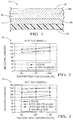
- Fig. 1 illustrates a non-limiting example of a ceramic-capacitor 10.
- the relative thickness of the layers illustrated is not meant to infer anything regarding relative thickness of the actual layers of materials used to form the ceramic-capacitor 10, but are only shown to easier visualize the description presented below.
- Other features of the ceramic-capacitor 10 are contemplated, but not illustrated, such as contacts or terminations that electrically connect the ceramic-capacitor 10 to other circuitry, as will be recognized by those skilled in the capacitor fabrication arts.
- the ceramic-capacitor 10 includes a substrate 12.
- the substrate 12 may be formed of a polymeric material such as APICAL® AV polyimide film from Kaneka Texas Corporation of Pasadena Texas, with a thickness of 50 micrometers (50 ⁇ m). Such polymeric substrates are commonly used in the fabrication of film-type capacitors and are suitable for use in high-volume, roll-to-roll, manufacturing processes. Alternatively, the substrate may be a metal foil.
- the ceramic-capacitor 10 also includes a first electrically-conductive-layer 14.
- the first electrically-conductive-layer 14 may be deposited by the known electron-beam evaporation process onto the substrate 12.
- the first electrically-conductive-layer 14 is aluminum, with a thickness of 100 nanometers (nm) to a thickness of 200 nm, and preferably 120 nm.
- the first electrically-conductive-layer 14 may be formed of platinum, copper, or nickel.
- a second electrically-conductive-layer 18 is arranged proximate to the first electrically-conductive-layer 14.
- the second electrically-conductive-layer 18 may be deposited by the known electron-beam evaporation process onto a dielectric-layer 16 (described below) that may overlay the first electrically-conductive-layer 14.
- the second electrically-conductive-layer 18 is aluminum, with a thickness of 100 nanometers (nm) to a thickness of 200 nm, and preferably 120 nm.
- the second electrically-conductive-layer 18 may be formed of platinum, copper, or nickel.
- the dielectric-layer 16 is interposed between the first electrically-conductive-layer 14 and the second electrically-conductive-layer 18, such that the first side 16A of the dielectric-layer 16 is in direct contact with the first electrically-conductive-layer 14, and the second side 16B of the dielectric-layer 16, opposite the first side, is in direct contact with second electrically-conductive-layer 18.
- the dielectric-layer 16 is formed of a lead-lanthanum-zirconium-titanate material (PLZT).
- PLZT is a ceramic material that has a relatively high dielectric constant when compared to other common dielectric materials, and is capable of operating at temperatures greater than 140° C.
- Empirical testing has indicated that a thickness for the PLZT layer of 8 ⁇ m provides for a good balance between reliability and dielectric breakdown, where the desired maximum capacitor voltage is 600 Volts.
- the PLZT, deposited according to the process described elsewhere herein, is generally observed to have a linear relationship of the dielectric constant over voltage, frequency and temperature, and is characterized by a dielectric constant greater than one-hundred-twenty-five (125), when measured at 25° C, zero Volts bias, and an excitation frequency of ten-thousand Hertz (10kHz).
- the dielectric constant is dimensionless, as it is defined as the ratio of the permittivity (in Farads per meter) of the dielectric material used in the capacitor, to the permittivity of a vacuum.
- Fig. 2 is a non-limiting example of a graph 40 that illustrates the increase in the dielectric constant of the PLZT, having an elemental ratio of Pb0.92/La0.08/Zr0.52/Ti0.48/O ⁇ , after heat-treating the ceramic-capacitor 10 for one hour (1-hour) at a temperature of 250° C, as will be described by the method, herein.
- the heat-treated PLZT is characterized by a relative permittivity or dielectric constant greater than 125 at 25° C, zero Volts bias, and an excitation frequency of 10kHz, compared to the non-heat-treated PLZT capacitor in the as-deposited, or zero-hour, state, which is less than 125 at 25° C, zero Volts bias, and an excitation frequency of 10kHz. It was discovered that the dielectric constant of the heat-treated PLZT was increased by twenty percent (20%) over the non-heat-treated PLZT. The details of the heat-treating process are described elsewhere herein. Note also the relatively linear relationship of the dielectric constant over the temperature range of -40° C to a temperature of 140° C, for both the non-heat-treated and heat-treated PLZT, as previously described.
- Fig. 3 is a non-limiting example of a graph 42 that illustrates the increase in the dielectric constant of the PLZT after the heat-treating of another sample of the ceramic-capacitor 10, fabricated by the same process, and containing the same elemental ratios, as the ceramic-capacitor 10 of Fig. 2 .
- the heat-treated PLZT is characterized by a dielectric constant of greater than 125 at 25° C, zero Volts bias, and an excitation frequency of 10kHz, compared to the non-heat-treated PLZT capacitor in the as-deposited, or zero-hour, state.
- the dielectric constant of the PLZT was increased by 32%, after heat-treating for 356-hours at a temperature of 250° C, over the non-heat-treated PLZT.
- the dielectric constant of the heat-treated PLZT was increased by 52% over the non-heat-treated PLZT.
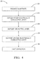
- Fig. 4 is a flowchart that illustrates a non-limiting example of a method 20 of fabricating and heat-treating the ceramic-capacitor 10 characterized by a dielectric constant of greater than 125 at 25° C, zero Volts bias, and an excitation frequency of 10kHz.
- Step 22, PROVIDE SUBSTRATE may include providing the substrate 12 formed of one of a glass, a ceramic, and a polymeric material.
- the substrate 12 may be formed of a polymeric material such as APICAL® AV polyimide film from Kaneka Texas Corporation of Pasadena Texas, with a thickness of 50 micrometers (50 ⁇ m).
- Such polymeric substrates are commonly used in the fabrication of film-type capacitors and are suitable for use in high-volume, roll-to-roll, manufacturing processes.
- the substrate may be a metal foil.
- Step 24, DEPOSIT FIRST ELECTRICALLY CONDUCTIVE LAYER may include depositing the first electrically-conductive-layer 14 on top of the substrate 12, formed of one of platinum, nickel, copper, and aluminum, utilizing an evaporative deposition process, such as electron-beam evaporation.
- the first electrically-conductive-layer 14 is aluminum, with a thickness of 100 nm to a thickness of 200 nm, and preferably 120 nm, which provides adequate electrical conductivity and flexibility.
- Step 26, DEPOSIT DIELECTRIC LAYER may include depositing the dielectric-layer 16 formed of PLZT deposited on top of the first electrically-conductive-layer 14 preferably using an aerosol spray process.
- the aerosol spray process may be performed at a deposition-temperature between 10° C and 38° C, and preferably room temperature, which advantageously requires neither heating nor cooling of the manufacturing facility.
- the velocity of impact of the submicron air-born PLZT particles generates the required heat to sinter the particles together upon deposition onto the first electrically-conductive-layer 14.
- PLZT is a ceramic material that has a high dielectric constant and is capable of operating at temperatures greater than 140° C.
- Empirical testing has indicated that a thickness for the PLZT layer of 8 ⁇ m provides for a good balance between dielectric breakdown and reliability, where the desired maximum capacitor voltage is 600 Volts.
- This deposition process is desirable in that the PLZT material is a ceramic that would typically require a firing process in excess of 650° C to sinter the particles into a solid monolithic structure.
- the firing temperatures required to sinter the PLZT particles would melt a polymer substrate 12.
- it is the ability to deposit the PLZT at temperatures not greater than the melting point of the polymer substrate 12 that enables the use of high-volume film processing methods for a ceramic-capacitor 10.
- Step 28 DEPOSIT SECOND ELECTRICALLY CONDUCTIVE LAYER, may include depositing the second electrically-conductive-layer 18 on top of the dielectric-layer 16, formed of one of platinum, nickel, copper, and aluminum, utilizing an evaporative deposition process, such as electron-beam evaporation.
- the second electrically-conductive-layer 18 is aluminum, with a thickness of 100 nm to a thickness of 200 nm, and preferably 120 nm, which provides adequate electrical conductivity and flexibility.
- Step 30, HEAT CAPACITOR may include heating the ceramic-capacitor 10 to a temperature not greater than 300° C. The heating may be conducted for a period of time such that the capacitance remains relatively linear as a function of voltage, frequency and temperature (much like a film capacitor), as opposed to the bell shaped curve that defines capacitance, of a traditional ceramic capacitor, as variable based on applied frequency, voltage or temperature. The capacitance of a traditional ceramic capacitor follows a bell shaped curve.
- the heating of ceramic-capacitor 10 may be performed in an oven where a controlled source of heat may include one of electric resistive elements, gas-fired burners, rapid thermal annealing, infrared and ultraviolet light sources, and a laser.
- a controlled source of heat may include one of electric resistive elements, gas-fired burners, rapid thermal annealing, infrared and ultraviolet light sources, and a laser.
- a ceramic-capacitor 10 and a method 20 of increasing the dielectric constant of the PLZT is provided.
- By increasing the dielectric constant of the PLZT less capacitive material is required to meet the targeted capacitance which, in turn, reduces the overall volume of the finished DC-link capacitor.
- it is the ability to deposit the PLZT at temperatures not greater than the melting point of the polymer substrate 12 that enables the use of high-volume film processing methods for a ceramic-capacitor 10.
- the ability to affect the dielectric constant by adjusting the heat-treating time and heat-treating temperature allows the ability to both increase the dielectric constant and reduce the variation of the population of dielectric constant values, without sacrificing the dielectric breakdown strength.
Landscapes
- Engineering & Computer Science (AREA)
- Chemical & Material Sciences (AREA)
- Power Engineering (AREA)
- Ceramic Engineering (AREA)
- Manufacturing & Machinery (AREA)
- Microelectronics & Electronic Packaging (AREA)
- Inorganic Chemistry (AREA)
- Materials Engineering (AREA)
- Structural Engineering (AREA)
- Organic Chemistry (AREA)
- Composite Materials (AREA)
- Fixed Capacitors And Capacitor Manufacturing Machines (AREA)
- Ceramic Capacitors (AREA)
Abstract
Description
- This disclosure generally relates to a ceramic-capacitor, and more particularly relates to a ceramic-capacitor with a lead-lanthanum-zirconium-titanate (PLZT) dielectric material.
- It is known that the high-voltage, DC-link capacitors used in electric vehicle invertors require large packaging volumes. In one example of a typical electric vehicle invertor, the DC-link capacitor is the heaviest single component, accounts for nearly forty percent (40%) of the total inverter volume, and is a significant portion of the inverter cost. DC-link capacitors are typically wound polypropylene film capacitors, with packaging volumes of greater than, or equal to, one liter. Disadvantageously, polypropylene film capacitors are limited in their service temperature by the film material, which can be as low as 85 degrees Celsius (85° C). In contrast, ceramic capacitors are capable of service temperatures of greater than 140° C, but require high firing temperatures in excess of 650° C to sinter the ceramic particles into a monolithic layer.
- Described herein is a ceramic-capacitor that can be fabricated with film manufacturing processes and heat-treated to significantly increase the dielectric constant of the lead-lanthanum-zirconium-titanate (PLZT) dielectric material, thereby greatly reducing the amount of capacitive material required to meet the targeted capacitance / voltage rating characteristics. The significant reduction in the amount of capacitive material will, in turn, greatly reduce the packaging volume of the DC-link capacitor.
- In accordance with one embodiment, a ceramic-capacitor is provided. The ceramic-capacitor includes a first electrically-conductive-layer. The ceramic-capacitor also includes a second electrically-conductive-layer arranged proximate to the first electrically-conductive-layer. The ceramic-capacitor also includes a dielectric-layer interposed between the first electrically-conductive-layer and the second electrically-conductive-layer. The dielectric-layer is formed of a lead-lanthanum-zirconium-titanate material (PLZT), wherein the PLZT is characterized by a dielectric-constant greater than 125 when measured at 25 degrees Celsius, zero Volts bias, and an excitation frequency of ten-thousand Hertz (10kHz).
- The dielectric-layer may be deposited using an aerosol spray process. A first side of the dielectric-layer may be in direct contact with the first electrically-conductive-layer, and a second side of the dielectric-layer opposite the first side may be in direct contact with the second electrically-conductive-layer.
- In another embodiment, a method for increasing a dielectric constant of lead-lanthanum-zirconium-titanate material (PLZT) is provided. The method includes the step of depositing PLZT to form a dielectric-layer of a ceramic-capacitor. The method also includes the step of heating the ceramic-capacitor to a temperature not greater than 300 degrees Celsius.
- The PLZT may be performed at a deposition-temperature between 10 degrees Celsius and 38 degrees Celsius
- Further features and advantages will appear more clearly on a reading of the following detailed description of the preferred embodiment, which is given by way of non-limiting example only and with reference to the accompanying drawings.
- The present invention will now be described, by way of example with reference to the accompanying drawings, in which:
-
Fig. 1 is a cross-sectional end view of a ceramic-capacitor in accordance with one embodiment; -
Fig. 2 is a graph showing an increase in the dielectric constant after heat-treating in accordance with one embodiment; -
Fig. 3 is a graph showing an increase in the dielectric constant after heat-treating in accordance with one embodiment; and -
Fig. 4 is a flowchart of a method for increasing a dielectric constant of the ceramic-capacitor ofFig. 1 in accordance with one embodiment. -
Fig. 1 illustrates a non-limiting example of a ceramic-capacitor 10. The relative thickness of the layers illustrated is not meant to infer anything regarding relative thickness of the actual layers of materials used to form the ceramic-capacitor 10, but are only shown to easier visualize the description presented below. Other features of the ceramic-capacitor 10 are contemplated, but not illustrated, such as contacts or terminations that electrically connect the ceramic-capacitor 10 to other circuitry, as will be recognized by those skilled in the capacitor fabrication arts. - The ceramic-
capacitor 10 includes asubstrate 12. Byway of example and not limitation, thesubstrate 12 may be formed of a polymeric material such as APICAL® AV polyimide film from Kaneka Texas Corporation of Pasadena Texas, with a thickness of 50 micrometers (50µm). Such polymeric substrates are commonly used in the fabrication of film-type capacitors and are suitable for use in high-volume, roll-to-roll, manufacturing processes. Alternatively, the substrate may be a metal foil. The ceramic-capacitor 10 also includes a first electrically-conductive-layer 14. By way of example and not limitation, the first electrically-conductive-layer 14 may be deposited by the known electron-beam evaporation process onto thesubstrate 12. Preferably the first electrically-conductive-layer 14 is aluminum, with a thickness of 100 nanometers (nm) to a thickness of 200 nm, and preferably 120 nm. Alternatively, the first electrically-conductive-layer 14 may be formed of platinum, copper, or nickel. - A second electrically-conductive-
layer 18 is arranged proximate to the first electrically-conductive-layer 14. By way of example and not limitation, the second electrically-conductive-layer 18 may be deposited by the known electron-beam evaporation process onto a dielectric-layer 16 (described below) that may overlay the first electrically-conductive-layer 14. Preferably the second electrically-conductive-layer 18 is aluminum, with a thickness of 100 nanometers (nm) to a thickness of 200 nm, and preferably 120 nm. Alternatively, the second electrically-conductive-layer 18 may be formed of platinum, copper, or nickel. - The dielectric-
layer 16 is interposed between the first electrically-conductive-layer 14 and the second electrically-conductive-layer 18, such that thefirst side 16A of the dielectric-layer 16 is in direct contact with the first electrically-conductive-layer 14, and thesecond side 16B of the dielectric-layer 16, opposite the first side, is in direct contact with second electrically-conductive-layer 18. The dielectric-layer 16 is formed of a lead-lanthanum-zirconium-titanate material (PLZT). PLZT is a ceramic material that has a relatively high dielectric constant when compared to other common dielectric materials, and is capable of operating at temperatures greater than 140° C. Empirical testing has indicated that a thickness for the PLZT layer of 8µm provides for a good balance between reliability and dielectric breakdown, where the desired maximum capacitor voltage is 600 Volts. The PLZT, deposited according to the process described elsewhere herein, is generally observed to have a linear relationship of the dielectric constant over voltage, frequency and temperature, and is characterized by a dielectric constant greater than one-hundred-twenty-five (125), when measured at 25° C, zero Volts bias, and an excitation frequency of ten-thousand Hertz (10kHz). The dielectric constant is dimensionless, as it is defined as the ratio of the permittivity (in Farads per meter) of the dielectric material used in the capacitor, to the permittivity of a vacuum. -
Fig. 2 is a non-limiting example of agraph 40 that illustrates the increase in the dielectric constant of the PLZT, having an elemental ratio of Pb0.92/La0.08/Zr0.52/Ti0.48/Oδ, after heat-treating the ceramic-capacitor 10 for one hour (1-hour) at a temperature of 250° C, as will be described by the method, herein. The heat-treated PLZT is characterized by a relative permittivity or dielectric constant greater than 125 at 25° C, zero Volts bias, and an excitation frequency of 10kHz, compared to the non-heat-treated PLZT capacitor in the as-deposited, or zero-hour, state, which is less than 125 at 25° C, zero Volts bias, and an excitation frequency of 10kHz. It was discovered that the dielectric constant of the heat-treated PLZT was increased by twenty percent (20%) over the non-heat-treated PLZT. The details of the heat-treating process are described elsewhere herein. Note also the relatively linear relationship of the dielectric constant over the temperature range of -40° C to a temperature of 140° C, for both the non-heat-treated and heat-treated PLZT, as previously described. -
Fig. 3 is a non-limiting example of agraph 42 that illustrates the increase in the dielectric constant of the PLZT after the heat-treating of another sample of the ceramic-capacitor 10, fabricated by the same process, and containing the same elemental ratios, as the ceramic-capacitor 10 ofFig. 2 . The heat-treated PLZT is characterized by a dielectric constant of greater than 125 at 25° C, zero Volts bias, and an excitation frequency of 10kHz, compared to the non-heat-treated PLZT capacitor in the as-deposited, or zero-hour, state. In this example, the dielectric constant of the PLZT was increased by 32%, after heat-treating for 356-hours at a temperature of 250° C, over the non-heat-treated PLZT. Upon further heat-treating for an additional 144-hours at a temperature of 300° C, the dielectric constant of the heat-treated PLZT was increased by 52% over the non-heat-treated PLZT. Note again the relatively linear relationship of the dielectric constant over the temperature range of -40° C to a temperature of 140° C, for both the non-heat-treated and heat-treated PLZT, as was previously described. Testing has indicated that the impact of heat-treating at temperatures greater than 300 °C resulted in a reduction in the dielectric breakdown strength. -
Fig. 4 is a flowchart that illustrates a non-limiting example of amethod 20 of fabricating and heat-treating the ceramic-capacitor 10 characterized by a dielectric constant of greater than 125 at 25° C, zero Volts bias, and an excitation frequency of 10kHz. -
Step 22, PROVIDE SUBSTRATE, may include providing thesubstrate 12 formed of one of a glass, a ceramic, and a polymeric material. By way of example and not limitation, thesubstrate 12 may be formed of a polymeric material such as APICAL® AV polyimide film from Kaneka Texas Corporation of Pasadena Texas, with a thickness of 50 micrometers (50µm). Such polymeric substrates are commonly used in the fabrication of film-type capacitors and are suitable for use in high-volume, roll-to-roll, manufacturing processes. Alternatively, the substrate may be a metal foil. -
Step 24, DEPOSIT FIRST ELECTRICALLY CONDUCTIVE LAYER, may include depositing the first electrically-conductive-layer 14 on top of thesubstrate 12, formed of one of platinum, nickel, copper, and aluminum, utilizing an evaporative deposition process, such as electron-beam evaporation. Preferably the first electrically-conductive-layer 14 is aluminum, with a thickness of 100 nm to a thickness of 200 nm, and preferably 120 nm, which provides adequate electrical conductivity and flexibility. -
Step 26, DEPOSIT DIELECTRIC LAYER, may include depositing the dielectric-layer 16 formed of PLZT deposited on top of the first electrically-conductive-layer 14 preferably using an aerosol spray process. The aerosol spray process may be performed at a deposition-temperature between 10° C and 38° C, and preferably room temperature, which advantageously requires neither heating nor cooling of the manufacturing facility. Preferably, the velocity of impact of the submicron air-born PLZT particles generates the required heat to sinter the particles together upon deposition onto the first electrically-conductive-layer 14. PLZT is a ceramic material that has a high dielectric constant and is capable of operating at temperatures greater than 140° C. Empirical testing has indicated that a thickness for the PLZT layer of 8µm provides for a good balance between dielectric breakdown and reliability, where the desired maximum capacitor voltage is 600 Volts. This deposition process is desirable in that the PLZT material is a ceramic that would typically require a firing process in excess of 650° C to sinter the particles into a solid monolithic structure. Using conventional ceramic processing methods, the firing temperatures required to sinter the PLZT particles would melt apolymer substrate 12. Advantageously, it is the ability to deposit the PLZT at temperatures not greater than the melting point of thepolymer substrate 12 that enables the use of high-volume film processing methods for a ceramic-capacitor 10. -
Step 28, DEPOSIT SECOND ELECTRICALLY CONDUCTIVE LAYER, may include depositing the second electrically-conductive-layer 18 on top of the dielectric-layer 16, formed of one of platinum, nickel, copper, and aluminum, utilizing an evaporative deposition process, such as electron-beam evaporation. Preferably the second electrically-conductive-layer 18 is aluminum, with a thickness of 100 nm to a thickness of 200 nm, and preferably 120 nm, which provides adequate electrical conductivity and flexibility. -
Step 30, HEAT CAPACITOR, may include heating the ceramic-capacitor 10 to a temperature not greater than 300° C. The heating may be conducted for a period of time such that the capacitance remains relatively linear as a function of voltage, frequency and temperature (much like a film capacitor), as opposed to the bell shaped curve that defines capacitance, of a traditional ceramic capacitor, as variable based on applied frequency, voltage or temperature. The capacitance of a traditional ceramic capacitor follows a bell shaped curve. - The heating of ceramic-
capacitor 10 may be performed in an oven where a controlled source of heat may include one of electric resistive elements, gas-fired burners, rapid thermal annealing, infrared and ultraviolet light sources, and a laser. - Accordingly, a ceramic-
capacitor 10, and amethod 20 of increasing the dielectric constant of the PLZT is provided. By increasing the dielectric constant of the PLZT, less capacitive material is required to meet the targeted capacitance which, in turn, reduces the overall volume of the finished DC-link capacitor. Additionally, it is the ability to deposit the PLZT at temperatures not greater than the melting point of thepolymer substrate 12 that enables the use of high-volume film processing methods for a ceramic-capacitor 10. The ability to affect the dielectric constant by adjusting the heat-treating time and heat-treating temperature allows the ability to both increase the dielectric constant and reduce the variation of the population of dielectric constant values, without sacrificing the dielectric breakdown strength. - While this invention has been described in terms of the preferred embodiments thereof, it is not intended to be so limited, but rather only to the extent set forth in the claims that follow.
Claims (5)
- A ceramic-capacitor (10) comprising:a first electrically-conductive-layer (14);a second electrically-conductive-layer (18) arranged proximate to the first electrically-conductive-layer (14); anda dielectric-layer (16) interposed between the first electrically-conductive-layer (14) and the second electrically-conductive-layer (18), said dielectric-layer (16) formed of a lead-lanthanum-zirconium-titanate material (PLZT), wherein the PLZT is characterized by a dielectric-constant greater than 125 when measured at 25 degrees Celsius, zero Volts bias, and an excitation frequency of ten-thousand Hertz (10kHz).
- The ceramic-capacitor (10) in accordance with claim 1 wherein the dielectric-layer (16) is deposited using an aerosol spray process.
- The ceramic-capacitor (10) according to any one of the preceding claims wherein a first side of the dielectric-layer (16) is in direct contact with the first electrically-conductive-layer (14), and a second side of the dielectric-layer (16) opposite the first side is in direct contact with the second electrically-conductive-layer (18).
- A method (20) for increasing a dielectric constant of lead-lanthanum-zirconium-titanate material (PLZT), said method (20) comprising:depositing PLZT to form a dielectric-layer (16) of a ceramic-capacitor (10); andheating the ceramic-capacitor (10) to a temperature not greater than 300 degrees Celsius.
- The method (20) of claim 4, wherein depositing the PLZT is performed at a deposition-temperature between 10 degrees Celsius and 38 degrees Celsius.
Applications Claiming Priority (1)
| Application Number | Priority Date | Filing Date | Title |
|---|---|---|---|
| US15/151,830 US9842695B2 (en) | 2016-05-11 | 2016-05-11 | PLZT capacitor and method to increase the dielectric constant |
Publications (2)
| Publication Number | Publication Date |
|---|---|
| EP3244428A2 true EP3244428A2 (en) | 2017-11-15 |
| EP3244428A3 EP3244428A3 (en) | 2017-11-29 |
Family
ID=58672432
Family Applications (1)
| Application Number | Title | Priority Date | Filing Date |
|---|---|---|---|
| EP17169639.6A Withdrawn EP3244428A3 (en) | 2016-05-11 | 2017-05-05 | Plzt capacitor and method to increase the dielectric constant |
Country Status (3)
| Country | Link |
|---|---|
| US (1) | US9842695B2 (en) |
| EP (1) | EP3244428A3 (en) |
| CN (1) | CN107369555B (en) |
Families Citing this family (1)
| Publication number | Priority date | Publication date | Assignee | Title |
|---|---|---|---|---|
| DE102020210516A1 (en) | 2020-08-19 | 2022-02-24 | Volkswagen Aktiengesellschaft | Conductor arrangement designed as a filter capacitor |
Family Cites Families (12)
| Publication number | Priority date | Publication date | Assignee | Title |
|---|---|---|---|---|
| JPS53116499A (en) * | 1977-03-23 | 1978-10-11 | Sharp Corp | Preparing high dielectric thin film |
| US4219866A (en) * | 1979-01-12 | 1980-08-26 | Sprague Electric Company | Ceramic capacitor having a dielectric of (Pb,La) (Zr,Ti)O3 and BaTiO3 |
| US5950292A (en) * | 1997-03-04 | 1999-09-14 | Sandia Corporation | Methods of fabricating applique circuits |
| US6623865B1 (en) * | 2000-03-04 | 2003-09-23 | Energenius, Inc. | Lead zirconate titanate dielectric thin film composites on metallic foils |
| TWI330672B (en) * | 2002-05-28 | 2010-09-21 | Nat Inst Of Advanced Ind Scien | Method for forming ultrafine particle brittle material at low temperature |
| KR100703077B1 (en) * | 2005-06-03 | 2007-04-06 | 삼성전기주식회사 | Method for manufacturing crystalline dielectric thin film, and crystalline dielectric thin film manufactured thereby and thin film capacitor having same |
| CN1937174A (en) * | 2005-07-11 | 2007-03-28 | E.I.内穆尔杜邦公司 | Capacitive devices, organic dielectric laminates, multilayer structures incorporating such devices, and methods of making thereof |
| WO2010137448A1 (en) * | 2009-05-29 | 2010-12-02 | 三洋電機株式会社 | Multilayer structure and method for manufacturing same |
| US8647737B2 (en) * | 2011-09-30 | 2014-02-11 | Uchicago Argonne, Llc | Method for fabrication of crack-free ceramic dielectric films |
| US9646766B2 (en) * | 2012-06-14 | 2017-05-09 | Uchicago Argonne, Llc | Method of making dielectric capacitors with increased dielectric breakdown strength |
| US9230739B2 (en) * | 2013-10-29 | 2016-01-05 | Uchicago Argonne, Llc | PLZT capacitor on glass substrate |
| US10128046B2 (en) * | 2014-06-16 | 2018-11-13 | Uchicago Argonne, Llc | Wound/stacked ceramic film capacitors, method for making ceramic film capacitors |
-
2016
- 2016-05-11 US US15/151,830 patent/US9842695B2/en active Active
-
2017
- 2017-05-05 EP EP17169639.6A patent/EP3244428A3/en not_active Withdrawn
- 2017-05-10 CN CN201710325781.5A patent/CN107369555B/en active Active
Non-Patent Citations (1)
| Title |
|---|
| None |
Also Published As
| Publication number | Publication date |
|---|---|
| US9842695B2 (en) | 2017-12-12 |
| EP3244428A3 (en) | 2017-11-29 |
| CN107369555B (en) | 2020-05-08 |
| US20170330685A1 (en) | 2017-11-16 |
| CN107369555A (en) | 2017-11-21 |
Similar Documents
| Publication | Publication Date | Title |
|---|---|---|
| CN102099880B (en) | Laminated ceramic electronic component and manufacturing method therefor | |
| EP4208698A1 (en) | Sensor element and method for producing a sensor element | |
| KR19980081733A (en) | Metal Deposition Film, Manufacturing Method and Capacitor Using the Same | |
| JP2014053589A (en) | Multilayer ceramic electronic component and manufacturing method therefor | |
| US9153380B2 (en) | Shapeable short circuit resistant capacitor | |
| JPH04118901A (en) | Positive temperature coefficient thermistor and its manufacture | |
| JP2013219094A (en) | Metalization film capacitor | |
| US20160027580A1 (en) | PLZT Capacitor On Glass Substrate | |
| US9842695B2 (en) | PLZT capacitor and method to increase the dielectric constant | |
| Alshatnawi et al. | High stability and reliability additively manufactured metal-insulator-metal capacitors for high-temperature applications | |
| Ma et al. | Flexible ceramic film capacitors for high-temperature power electronics | |
| WO2024079096A1 (en) | Sensor element and method for producing a sensor element | |
| JP4915947B2 (en) | Metallized film capacitors | |
| JPH098246A (en) | Semiconductor device and manufacturing method thereof | |
| FR3058256A1 (en) | ALUMINA CERAMIC-BASED ELECTRICAL INSULATION, METHOD FOR PRODUCING THE INSULATOR, AND VACUUM TUBE COMPRISING THE INSULATION | |
| JP2017037956A (en) | Metallized film capacitors | |
| CA2885675A1 (en) | Method for producing a capacitor and capacitor | |
| Heidary et al. | Redesigning multilayer ceramic capacitors by preservation of electrode conductivity and localized doping | |
| JP5974275B2 (en) | Film capacitor | |
| US20130215552A1 (en) | Laminated electronic component and manufacturing method thereof | |
| KR100302106B1 (en) | Metal deposition film for capacitor with two reinforcement layers and manufacturing method | |
| KR20020068561A (en) | Plastic film of metal evaporation and condenser manufactured method using thereof | |
| JPH02222129A (en) | Film capacitor and manufacture thereof | |
| JP2007109845A (en) | Metal-deposited film for capacitors and capacitors | |
| JP2010182859A (en) | Metal deposited film and manufacturing method of the same |
Legal Events
| Date | Code | Title | Description |
|---|---|---|---|
| PUAI | Public reference made under article 153(3) epc to a published international application that has entered the european phase |
Free format text: ORIGINAL CODE: 0009012 |
|
| PUAL | Search report despatched |
Free format text: ORIGINAL CODE: 0009013 |
|
| AK | Designated contracting states |
Kind code of ref document: A2 Designated state(s): AL AT BE BG CH CY CZ DE DK EE ES FI FR GB GR HR HU IE IS IT LI LT LU LV MC MK MT NL NO PL PT RO RS SE SI SK SM TR |
|
| AX | Request for extension of the european patent |
Extension state: BA ME |
|
| AK | Designated contracting states |
Kind code of ref document: A3 Designated state(s): AL AT BE BG CH CY CZ DE DK EE ES FI FR GB GR HR HU IE IS IT LI LT LU LV MC MK MT NL NO PL PT RO RS SE SI SK SM TR |
|
| AX | Request for extension of the european patent |
Extension state: BA ME |
|
| RIC1 | Information provided on ipc code assigned before grant |
Ipc: C04B 35/01 20060101ALI20171025BHEP Ipc: H01G 4/08 20060101ALI20171025BHEP Ipc: H01G 4/12 20060101AFI20171025BHEP Ipc: H01G 4/33 20060101ALI20171025BHEP Ipc: H01L 49/02 20060101ALI20171025BHEP |
|
| STAA | Information on the status of an ep patent application or granted ep patent |
Free format text: STATUS: THE APPLICATION IS DEEMED TO BE WITHDRAWN |
|
| 18D | Application deemed to be withdrawn |
Effective date: 20180530 |
|
| RIC1 | Information provided on ipc code assigned before grant |
Ipc: H01G 4/12 20060101AFI20181022BHEP Ipc: H01L 49/02 20060101ALI20181022BHEP Ipc: C04B 35/01 20060101ALI20181022BHEP Ipc: H01G 4/08 20060101ALI20181022BHEP Ipc: H01G 4/33 20060101ALI20181022BHEP |