EP3244281A1 - An on chip temperature independent current generator - Google Patents
An on chip temperature independent current generator Download PDFInfo
- Publication number
- EP3244281A1 EP3244281A1 EP16169716.4A EP16169716A EP3244281A1 EP 3244281 A1 EP3244281 A1 EP 3244281A1 EP 16169716 A EP16169716 A EP 16169716A EP 3244281 A1 EP3244281 A1 EP 3244281A1
- Authority
- EP
- European Patent Office
- Prior art keywords
- chip
- current
- current generator
- temperature independent
- ptat
- Prior art date
- Legal status (The legal status is an assumption and is not a legal conclusion. Google has not performed a legal analysis and makes no representation as to the accuracy of the status listed.)
- Granted
Links
Images


Classifications
-
- G—PHYSICS
- G05—CONTROLLING; REGULATING
- G05F—SYSTEMS FOR REGULATING ELECTRIC OR MAGNETIC VARIABLES
- G05F3/00—Non-retroactive systems for regulating electric variables by using an uncontrolled element, or an uncontrolled combination of elements, such element or such combination having self-regulating properties
- G05F3/02—Regulating voltage or current
- G05F3/08—Regulating voltage or current wherein the variable is DC
- G05F3/10—Regulating voltage or current wherein the variable is DC using uncontrolled devices with non-linear characteristics
- G05F3/16—Regulating voltage or current wherein the variable is DC using uncontrolled devices with non-linear characteristics being semiconductor devices
- G05F3/20—Regulating voltage or current wherein the variable is DC using uncontrolled devices with non-linear characteristics being semiconductor devices using diode- transistor combinations
- G05F3/26—Current mirrors
- G05F3/267—Current mirrors using both bipolar and field-effect technology
-
- G—PHYSICS
- G05—CONTROLLING; REGULATING
- G05F—SYSTEMS FOR REGULATING ELECTRIC OR MAGNETIC VARIABLES
- G05F1/00—Automatic systems in which deviations of an electric quantity from one or more predetermined values are detected at the output of the system and fed back to a device within the system to restore the detected quantity to its predetermined value or values, i.e. retroactive systems
- G05F1/10—Regulating voltage or current
- G05F1/46—Regulating voltage or current wherein the variable actually regulated by the final control device is DC
- G05F1/462—Regulating voltage or current wherein the variable actually regulated by the final control device is DC as a function of the requirements of the load, e.g. delay, temperature, specific voltage/current characteristic
- G05F1/463—Sources providing an output which depends on temperature
Definitions
- the invention relates to an on chip temperature independent current generator for generating a temperature independent current which can be supplied to other circuit elements of an integrated circuit.
- thermo independent current generators comprising current DACs and a set of current mirrors in which a first current proportional to the absolute temperature and a second current complementary to the absolute temperature are mixed in proper proportion to provide a temperature independent current.
- providing a temperature independent current this way requires a precise trimming of the temperature dependency compensation.
- the invention provides an on chip temperature independent current generator for generating a temperature independent current
- said on chip temperature independent current generator comprises an on chip current generator having an output to provide an electrical current being proportional to an absolute temperature of the chip, an on chip transistor having a base connected to a temperature independent reference voltage generator, a collector connected to a current mirror and an emitter connected to the output of the on chip current generator and connected via an on chip resistor to a reference potential, wherein the current mirror is adapted to mirror a collector current flowing to the collector of said on chip transistor to generate the temperature independent current.
- the on chip transistor comprises an on chip bipolar NPN transistor.
- the current mirror comprises a CMOS or BJT current mirror.
- the on chip current generator comprises an operation amplifier having an inverting input to which a first bipolar transistor is connected and a non-inverting input to which a second bipolar transistor is connected via a resistor having a predetermined resistance and having an output connected to an integrated CMOS current mirror of said on chip current generator.
- the on chip resistor is of the same type as the resistor of the on chip current generator.
- the on chip resistor has a resistance being m times the resistance of the resistor of said on chip current generator, wherein m is a positive real number.
- the resistance of the resistor of said on chip current generator is dependent on the temperature of said chip.
- the resistance of the resistor of said on chip current generator is temperature independent.
- the current generated by said temperature independent current generator is temperature independent in a wide temperature range between about -60° Celsius and about +200° Celsius.
- the current generated by the temperature independent current generator comprises a nominal current amplitude in a range of about 0,6 to 1,0 ⁇ Amp.
- an on chip temperature independent current generator 1 is configured to generate a temperature independent current output by the on chip temperature independent current generator 1 at an output terminal 2 as illustrated in Fig. 1 .
- the on chip temperature independent current generator 1 comprises in the illustrated embodiment an on chip current generator 3 having an output 4 to provide an electrical current I PTAT having a current amplitude being proportional to an absolute temperature T of the chip.
- the output 4 of the on chip current generator 4 is connected via a line 5 to an internal node 6 connected to the emitter E of an on chip transistor 9 which is formed in the illustrated embodiment by an on chip bipolar NPN transistor.
- the on chip transistor 9 has a base B connected to a temperature independent reference voltage generator 10 via an internal line 11.
- the temperature independent reference voltage generator 10 can be in a possible embodiment formed by a band gap voltage generator.
- the on chip transistor 9 further comprises a collector C connected to a current mirror 12 via a line 13.
- the on chip transistor 9 comprises an emitter E connected to the internal node 6 and connected via the line 5 to the output 4 of the on chip current generator 3.
- the emitter E of the on chip transistor 9 is further connected via an on chip resistor 14 to a reference potential GND (Ground).
- the current mirror 12 is adapted to mirror the collector current I C flowing through the collector C of the on chip transistor 9 to generate the temperature independent current I out at the output terminal 2 of the on chip temperature independent current generator 1.
- the current mirror 12 is in a preferred embodiment a CMOS current mirror or a BJT current mirror.
- the on chip independent reference voltage generator 10 can be in a possible embodiment formed by an on chip reference voltage generator integrated on the chip. In an alternative embodiment, the reference voltage generator 10 can also be formed by an external voltage reference source.
- the current mirror 12 can be adapted to mirror, multiply and/or replicate the collector current I C of the on chip bipolar NPN transistor 9.
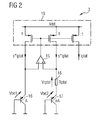
- the on chip current generator 3 can be implemented in a possible exemplary embodiment by a circuit as illustrated in Fig. 2 .
- the on chip current generator 3 comprises an operation amplifier 15 having an inverting input (-) and a non-inverting input (+).
- the inverting input (-) of the operation amplifier 15 is connected to a first bipolar transistor 16 and the non-inverting input (+) of the operation amplifier 15 is connected to a second bipolar transistor 17 via a resistor 18 as illustrated in Fig. 2 .
- the resistor 18 comprises a predetermined resistance R PTAT .
- the operation amplifier 15 comprises an output connected to an integrated CMOS current mirror 19 of the on chip current generator 3.
- the on chip resistor 14 as illustrated in Fig.
- the on chip resistor 14 comprises in a possible embodiment a resistance m*R PTAT being m times the resistance R PTAT of the resistor 18 of the on chip current generator 3 wherein m is an integer number equal or greater than 1.
- the resistance R PTAT of the resistor 18 of the on chip current generator 3 as illustrated in Fig. 2 is in a possible embodiment dependent on the temperature T of the chip. In an alternative embodiment, the resistance R PTAT of the resistor 18 of the on chip current generator 3 is temperature independent.
- the current I out generated by the temperature independent current generator 1 is in a possible embodiment temperature independent in a wide temperature range between e.g. about -60° Celsius and about +200° Celsius.
- the generated temperature independent current I out at the output terminal 2 of the on chip temperature independent current generator 1 can comprise in a possible embodiment a nominal current amplitude in a range of about 0,6 to 1,0 ⁇ Amp.
- the base emitter voltage V be 1 of the bipolar transistor 16 is equal to the base emitter voltage V be2 of the second bipolar transistor 17 reduced by the voltage drop across the resistor 18:
- V be 1 V be 2 + V rptat
- Expression (9) is a formula for calculating the generated current I PTAT output by the on chip current generator 3 at the output 4 via the line 5 to the internal node 6 of the on chip temperature independent current generator 1.
- the generated electrical current I PTAT depends on design parameters n, s, R PTAT and a physical parameter, i.e. the temperature T in Kelvin.
- the output current I out has the same temperature dependency as the collector current I C . Accordingly, it is sufficient to make the collector current I C temperature independent.
- I C V REF ⁇ V BEQ 0 m * R PTAT + T * ⁇ V BEQ m * R PTAT ⁇ K * T e * 1 n n * / s * R PTAT
- the resistance of the resistor 18 can be either temperature independent or temperature dependent.
- the resistance R PTAT of the resistor 18 is temperature dependent.
- the resistance of the resistor can have a first order temperature coefficient T C . Further, order temperature coefficients can be ignored because of their small influence.
- R PTAT R PTAT 0 * 1 + T C * T wherein R PTAT0 is the resistor value at 0°K.
- I C * m * R PTAT 0 V REF ⁇ V BEQ 0 1 + T C * T + T * ⁇ V BEQ 1 + T C * T ⁇ K * T * m e * s * 1 + T C * T * 1 n n
- Fig. 3 is a diagram illustrating the temperature dependency of an electrical current generated by a conventional current generator and by an embodiment of an on chip temperature independent current generator 1 according to the present invention.
- the curve I illustrates the current I generated by the on chip temperature independent current generator 1 in a wide temperature range between about -60° Celsius and about +200° Celsius.
- Curve II illustrates an electrical current provided by a conventional current generator.
- the current I out generated by the temperature independent current generator 1 according to the present invention (curve I) is almost completely temperature independent in the wide temperature range between -60° Celsius and +200° Celsius.
- the conventional current generator (curve II) generates a temperature dependent current. With increasing temperature, the current generated by the conventional current generator increases steadily.
- Fig. 3 shows a simulation plot of the generated currents depending on temperature T of the chip.
- the current I out generated by the temperature independent current generator 1 comprises a nominal current amplitude of about 0,8 ⁇ Amp, i.e. in a range of about 0,6 to 1,0 ⁇ Amp.
Landscapes
- Engineering & Computer Science (AREA)
- Physics & Mathematics (AREA)
- Electromagnetism (AREA)
- General Physics & Mathematics (AREA)
- Radar, Positioning & Navigation (AREA)
- Automation & Control Theory (AREA)
- Microelectronics & Electronic Packaging (AREA)
- Nonlinear Science (AREA)
- Control Of Electrical Variables (AREA)
Abstract
Description
- The invention relates to an on chip temperature independent current generator for generating a temperature independent current which can be supplied to other circuit elements of an integrated circuit.
- Conventional current generators which can generate a temperature independent current can be based on voltage to current converter circuits and require a temperature independent reference voltage band gap as well as a temperature independent resistance. However, it is difficult to implement this kind of current generator in CMOS technology.
- Further, there are known conventional temperature independent current generators comprising current DACs and a set of current mirrors in which a first current proportional to the absolute temperature and a second current complementary to the absolute temperature are mixed in proper proportion to provide a temperature independent current. However, providing a temperature independent current this way requires a precise trimming of the temperature dependency compensation.
- Accordingly, it is an object to provide an on chip temperature independent current generator which does not require a trimming.
- This object is achieved by an on chip temperature independent current generator comprising the features of claim 1.
- The invention provides an on chip temperature independent current generator for generating a temperature independent current wherein said on chip temperature independent current generator comprises
an on chip current generator having an output to provide an electrical current being proportional to an absolute temperature of the chip,
an on chip transistor having a base connected to a temperature independent reference voltage generator, a collector connected to a current mirror and an emitter connected to the output of the on chip current generator and connected via an on chip resistor to a reference potential,
wherein the current mirror is adapted to mirror a collector current flowing to the collector of said on chip transistor to generate the temperature independent current. - In a possible embodiment of the on chip temperature independent current generator according to the present invention, the on chip transistor comprises an on chip bipolar NPN transistor.
- In a further possible embodiment of the on chip temperature independent current generator according to the present invention, the current mirror comprises a CMOS or BJT current mirror.
- In a further possible embodiment of the on chip temperature independent current generator according to the present invention, the on chip current generator comprises an operation amplifier having an inverting input to which a first bipolar transistor is connected and a non-inverting input to which a second bipolar transistor is connected via a resistor having a predetermined resistance and having an output connected to an integrated CMOS current mirror of said on chip current generator.
- In a further possible embodiment of the on chip temperature independent current generator according to the present invention, the on chip resistor is of the same type as the resistor of the on chip current generator.
- In a further possible embodiment of the on chip temperature independent current generator according to the present invention, the on chip resistor has a resistance being m times the resistance of the resistor of said on chip current generator, wherein m is a positive real number.
- In a still further possible embodiment of the on chip temperature independent current generator according to the first aspect of the present invention, the resistance of the resistor of said on chip current generator is dependent on the temperature of said chip.
- In a still further possible embodiment of the on chip temperature independent current generator according to the present invention, the resistance of the resistor of said on chip current generator is temperature independent.
- In a further possible embodiment of the on chip temperature independent current generator according to the present invention, the current generated by said temperature independent current generator is temperature independent in a wide temperature range between about -60° Celsius and about +200° Celsius.
- In a further possible embodiment of the on chip temperature independent current generator according to the present invention, the current generated by the temperature independent current generator comprises a nominal current amplitude in a range of about 0,6 to 1,0 µAmp.
- In the following, possible embodiments of the on chip temperature independent current generator according to the present invention are described in more detail with reference to the enclosed figures.
- Fig. 1
- shows a circuit diagram for illustrating a possible exemplary embodiment of an on chip temperature independent current generator according to the present invention;
- Fig. 2
- shows a circuit diagram of a possible exemplary implementation of an on chip current generator integrated in the on chip temperature independent current generator according to the present invention as illustrated in the embodiment of
Fig. 1 ; - Fig. 3
- shows a diagram for illustrating the operation of an on chip temperature independent current generator according to the present invention in comparison to a conventional current generator.
- As can be seen in
Fig. 1 , an on chip temperature independent current generator 1 is configured to generate a temperature independent current output by the on chip temperature independent current generator 1 at anoutput terminal 2 as illustrated inFig. 1 . The on chip temperature independent current generator 1 comprises in the illustrated embodiment an on chipcurrent generator 3 having an output 4 to provide an electrical current IPTAT having a current amplitude being proportional to an absolute temperature T of the chip. The output 4 of the on chip current generator 4 is connected via a line 5 to aninternal node 6 connected to the emitter E of an onchip transistor 9 which is formed in the illustrated embodiment by an on chip bipolar NPN transistor. The onchip transistor 9 has a base B connected to a temperature independentreference voltage generator 10 via aninternal line 11. The temperature independentreference voltage generator 10 can be in a possible embodiment formed by a band gap voltage generator. The onchip transistor 9 further comprises a collector C connected to acurrent mirror 12 via aline 13. The onchip transistor 9 comprises an emitter E connected to theinternal node 6 and connected via the line 5 to the output 4 of the on chipcurrent generator 3. The emitter E of the onchip transistor 9 is further connected via an onchip resistor 14 to a reference potential GND (Ground). Thecurrent mirror 12 is adapted to mirror the collector current IC flowing through the collector C of the onchip transistor 9 to generate the temperature independent current Iout at theoutput terminal 2 of the on chip temperature independent current generator 1. Thecurrent mirror 12 is in a preferred embodiment a CMOS current mirror or a BJT current mirror. The on chip independentreference voltage generator 10 can be in a possible embodiment formed by an on chip reference voltage generator integrated on the chip. In an alternative embodiment, thereference voltage generator 10 can also be formed by an external voltage reference source. Thecurrent mirror 12 can be adapted to mirror, multiply and/or replicate the collector current IC of the on chipbipolar NPN transistor 9. - The on chip
current generator 3 can be implemented in a possible exemplary embodiment by a circuit as illustrated inFig. 2 . In the illustrated embodiment, the on chipcurrent generator 3 comprises anoperation amplifier 15 having an inverting input (-) and a non-inverting input (+). In a possible embodiment, the inverting input (-) of theoperation amplifier 15 is connected to a firstbipolar transistor 16 and the non-inverting input (+) of theoperation amplifier 15 is connected to a secondbipolar transistor 17 via aresistor 18 as illustrated inFig. 2 . Theresistor 18 comprises a predetermined resistance RPTAT. Theoperation amplifier 15 comprises an output connected to an integrated CMOScurrent mirror 19 of the on chipcurrent generator 3. The onchip resistor 14 as illustrated inFig. 1 is in a preferred embodiment of the same type and/or material as theresistor 18 of the on chipcurrent generator 3. The onchip resistor 14 comprises in a possible embodiment a resistance m*RPTAT being m times the resistance RPTAT of theresistor 18 of the on chipcurrent generator 3 wherein m is an integer number equal or greater than 1. The resistance RPTAT of theresistor 18 of the on chipcurrent generator 3 as illustrated inFig. 2 is in a possible embodiment dependent on the temperature T of the chip. In an alternative embodiment, the resistance RPTAT of theresistor 18 of the on chipcurrent generator 3 is temperature independent. - The current Iout generated by the temperature independent current generator 1 is in a possible embodiment temperature independent in a wide temperature range between e.g. about -60° Celsius and about +200° Celsius. The generated temperature independent current Iout at the
output terminal 2 of the on chip temperature independent current generator 1 can comprise in a possible embodiment a nominal current amplitude in a range of about 0,6 to 1,0 µAmp. - As can be seen in the circuit diagram of
Fig. 2 , the base emitter voltage V be1 of thebipolar transistor 16 is equal to the base emitter voltage Vbe2 of the secondbipolar transistor 17 reduced by the voltage drop across the resistor 18:
- The
current mirror 19 supplies theresistor 18 with a current s*IPTAT as shown inFig. 2 so that the voltage drop across theresistor 18 is given by:
- The base emitter voltage Vbe across the
bipolar transistors 

- Further,

- K is a Boltzmann constant
- T is the temperature in Kelvin and
- e is the charge of an electron.
- Is is the temperature current of a pn-junction of a bipolar transistor,
- s is the number of the current mirror sections in the PTAT current generator.
- Consequently:


- Expression (9) is a formula for calculating the generated current IPTAT output by the on chip
current generator 3 at the output 4 via the line 5 to theinternal node 6 of the on chip temperature independent current generator 1. The generated electrical current IPTAT depends on design parameters n, s, RPTAT and a physical parameter, i.e. the temperature T in Kelvin. - The
resistor 14 is of the same type and/or material as theresistor 18 used for the PTAT current generator 3:
resistor 14 and RPTAT is the resistance ofresistor 18 and m can be any positive real number. - The output current Iout can be a replica or multiplied product of the current IPTAT:

- The output current Iout has the same temperature dependency as the collector current IC. Accordingly, it is sufficient to make the collector current IC temperature independent.
- Based on the first Kirchhoff law and ignoring the base current IB of the
NPN transistor 9 gives:



- The collector current IC can be expressed as follows:

- VBEQ is the voltage between the base B and the emitter E terminals of the
bipolar transistor 9. This voltage can have a negative temperature dependency ΔVbeq around 2 mV/Kelvin. Because of the small temperature dependency, it is possible to write:
transistor 9 at 0°K. - Using the equation (9) one can re-write equation (16) in the following way:

- The resistance of the
resistor 18 can be either temperature independent or temperature dependent. - To provide a temperature independent current by the on chip temperature independent current generator 1 it is necessary that the collector current IC is temperature independent. By differentiating both sides of
equation 18 with the temperature T and by assuming that the reference voltage VREF provided by the temperature independentreference voltage generator 10 and the voltage VBEQ0 are constant one arrives to the following equation:
- Equation (19) can be rewritten as:

- Equation (20) can be rewritten as follows:

- Accordingly, by knowing the voltage ΔVbeq from a technology specification and by fixing two of the three free selectable design parameters m, n, s, it is possible to determine the third design parameter from equation (21) such that the collector current IC is temperature independent.
- In a second alternative embodiment, the resistance RPTAT of the
resistor 18 is temperature dependent. In this case, the resistance of the resistor can have a first order temperature coefficient TC. Further, order temperature coefficients can be ignored because of their small influence. - The resistance RPTAT of the
resistor 18 can be written as follows:
- Rewriting equation (18) leads to the following equation:


- Since m*RPTAT0 is constant, both sides of equation (24) can be multiplied with this value:

- Differentiating equation (25) on both sides with the temperature T gives:


- From this follows:

- Consequently, by knowing ΔVbeq, VBEQ0 and the temperature coefficient TC from the technology specification, it is possible by fixing two of the three free selectable design parameters m, n, s to determine the third design parameter from equation (29) such that the collector current IC becomes temperature independent.
-
Fig. 3 is a diagram illustrating the temperature dependency of an electrical current generated by a conventional current generator and by an embodiment of an on chip temperature independent current generator 1 according to the present invention. The curve I illustrates the current I generated by the on chip temperature independent current generator 1 in a wide temperature range between about -60° Celsius and about +200° Celsius. Curve II illustrates an electrical current provided by a conventional current generator. As can be seen from the curves illustrated inFig. 3 , the current Iout generated by the temperature independent current generator 1 according to the present invention (curve I) is almost completely temperature independent in the wide temperature range between -60° Celsius and +200° Celsius. In contrast, the conventional current generator (curve II) generates a temperature dependent current. With increasing temperature, the current generated by the conventional current generator increases steadily.Fig. 3 shows a simulation plot of the generated currents depending on temperature T of the chip. As can be seen fromFig. 3 , the current Iout generated by the temperature independent current generator 1 comprises a nominal current amplitude of about 0,8 µAmp, i.e. in a range of about 0,6 to 1,0 µAmp.
Claims (9)
- An on chip temperature independent current generator, TICG, (1) for generating a temperature independent current (Iout),
said TICG (1) comprising:- an on chip current generator (3) having an output (4) to provide an electrical current (IPTAT) being proportional to an absolute temperature (T) of said chip;- an on chip transistor (9) having a base (B) connected to a temperature independent reference voltage generator (10), a collector (C) connected to a current mirror (12) and an emitter (E) connected to the output (4) of the on chip current generator (3) and connected via an on chip resistor (14) to a reference potential (GND);- wherein the current mirror (12) is adapted to mirror a collector current (Ic) flowing to the collector (C) of said on chip transistor (9) to generate the temperature independent current (Iout). - The on chip temperature independent current generator according to claim 1, wherein said on chip transistor (9) is an on chip bipolar NPN transistor.
- The on chip temperature independent current generator according to claim 1 and 2, wherein said current mirror (12) is a CMOS or BJT current mirror.
- The on chip temperature independent current generator according to any of the preceding claims 1 to 3, wherein said on chip current generator (3) comprises an operation amplifier (15) having an inverting input (-) to which a first bipolar transistor (10) is connected and a non-inverting input (+) to which a second bipolar transistor (17) is connected via a resistor (18) having a predetermined resistance (RPTAT) and having an output connected to an integrated CMOS current mirror (19) of said on chip current generator (3).
- The on chip temperature independent current generator according to claim 4, wherein said on chip resistor (14) is of the same type as the resistor (18) of said on chip current generator (3).
- The on chip temperature independent current generator according to claim 5, wherein said on chip resistor (14) has a resistance (mRPTAT) being m times the resistance (RPTAT) of the resistor (18) of said on chip current generator (3), wherein m is a positive real number.
- The on chip temperature independent current generator according to any of the preceding claims 1 to 6, wherein the resistance (RPTAT) of the resistor (18) of said on chip current generator (3) is dependent on the temperature (T) of said chip.
- The on chip temperature independent current generator according to any of the preceding claims 1 to 6, wherein the resistance (RPTAT) of the resistor (18) of said on chip current generator (3) is temperature independent.
- The on chip temperature independent current generator according to any of the preceding claims 1 to 8, wherein the current (Iout) generated by said temperature independent current generator, TICG, (1) is temperature independent in a wide temperature range between about -60° Celsius and about +200° Celsius.
Priority Applications (2)
| Application Number | Priority Date | Filing Date | Title |
|---|---|---|---|
| EP16169716.4A EP3244281B1 (en) | 2016-05-13 | 2016-05-13 | An on chip temperature independent current generator |
| US15/592,596 US10042378B2 (en) | 2016-05-13 | 2017-05-11 | On chip temperature independent current generator |
Applications Claiming Priority (1)
| Application Number | Priority Date | Filing Date | Title |
|---|---|---|---|
| EP16169716.4A EP3244281B1 (en) | 2016-05-13 | 2016-05-13 | An on chip temperature independent current generator |
Publications (2)
| Publication Number | Publication Date |
|---|---|
| EP3244281A1 true EP3244281A1 (en) | 2017-11-15 |
| EP3244281B1 EP3244281B1 (en) | 2022-07-20 |
Family
ID=56014842
Family Applications (1)
| Application Number | Title | Priority Date | Filing Date |
|---|---|---|---|
| EP16169716.4A Active EP3244281B1 (en) | 2016-05-13 | 2016-05-13 | An on chip temperature independent current generator |
Country Status (2)
| Country | Link |
|---|---|
| US (1) | US10042378B2 (en) |
| EP (1) | EP3244281B1 (en) |
Families Citing this family (2)
| Publication number | Priority date | Publication date | Assignee | Title |
|---|---|---|---|---|
| US12068747B2 (en) * | 2021-08-12 | 2024-08-20 | Taiwan Semiconductor Manufacturing Company, Ltd. | Semiconductor device and method of monitoring a temperature thereof |
| TWI831526B (en) * | 2022-12-16 | 2024-02-01 | 天鈺科技股份有限公司 | Bandgap reference circuit and method of generating reference voltage and reference current simultaneously |
Citations (3)
| Publication number | Priority date | Publication date | Assignee | Title |
|---|---|---|---|---|
| US20080136504A1 (en) * | 2006-12-07 | 2008-06-12 | Young Ho Kim | Low-voltage band-gap reference voltage bias circuit |
| US7728575B1 (en) * | 2008-12-18 | 2010-06-01 | Texas Instruments Incorporated | Methods and apparatus for higher-order correction of a bandgap voltage reference |
| WO2013133733A1 (en) * | 2012-03-05 | 2013-09-12 | Freescale Semiconductor, Inc | Reference voltage source and method for providing a curvature-compensated reference voltage |
Family Cites Families (4)
| Publication number | Priority date | Publication date | Assignee | Title |
|---|---|---|---|---|
| US6087820A (en) * | 1999-03-09 | 2000-07-11 | Siemens Aktiengesellschaft | Current source |
| US7915882B2 (en) * | 2007-09-17 | 2011-03-29 | Texas Instruments Incorporated | Start-up circuit and method for a self-biased zero-temperature-coefficient current reference |
| US8710901B2 (en) * | 2012-07-23 | 2014-04-29 | Lsi Corporation | Reference circuit with curvature correction using additional complementary to temperature component |
| US9246479B2 (en) * | 2014-01-20 | 2016-01-26 | Via Technologies, Inc. | Low-offset bandgap circuit and offset-cancelling circuit therein |
-
2016
- 2016-05-13 EP EP16169716.4A patent/EP3244281B1/en active Active
-
2017
- 2017-05-11 US US15/592,596 patent/US10042378B2/en active Active
Patent Citations (3)
| Publication number | Priority date | Publication date | Assignee | Title |
|---|---|---|---|---|
| US20080136504A1 (en) * | 2006-12-07 | 2008-06-12 | Young Ho Kim | Low-voltage band-gap reference voltage bias circuit |
| US7728575B1 (en) * | 2008-12-18 | 2010-06-01 | Texas Instruments Incorporated | Methods and apparatus for higher-order correction of a bandgap voltage reference |
| WO2013133733A1 (en) * | 2012-03-05 | 2013-09-12 | Freescale Semiconductor, Inc | Reference voltage source and method for providing a curvature-compensated reference voltage |
Also Published As
| Publication number | Publication date |
|---|---|
| US20170329362A1 (en) | 2017-11-16 |
| EP3244281B1 (en) | 2022-07-20 |
| US10042378B2 (en) | 2018-08-07 |
Similar Documents
| Publication | Publication Date | Title |
|---|---|---|
| US7750728B2 (en) | Reference voltage circuit | |
| CN207457889U (en) | Pedestal generator circuit and circuit system | |
| CN101859158B (en) | Reference current circuit and reference current generation method | |
| EP2480947B1 (en) | Compensated bandgap | |
| US8269548B2 (en) | Zero-temperature-coefficient voltage or current generator | |
| CN102369495B (en) | Method and circuit for low power voltage reference and bias current generator | |
| US7636009B2 (en) | Bias current generating apparatus with adjustable temperature coefficient | |
| US8587368B2 (en) | Bandgap reference circuit with an output insensitive to offset voltage | |
| JP2007157055A (en) | Reference voltage generation circuit | |
| JP2004146576A (en) | Semiconductor temperature measuring circuit | |
| TW201533559A (en) | Voltage reference circuit | |
| US7161340B2 (en) | Method and apparatus for generating N-order compensated temperature independent reference voltage | |
| TW586000B (en) | Temperature detection circuit and method | |
| US7511567B2 (en) | Bandgap reference voltage circuit | |
| US6507238B1 (en) | Temperature-dependent reference generator | |
| JP2001510609A (en) | Reference voltage source with temperature compensated output reference voltage | |
| CN103365330A (en) | Reference voltage/current generator | |
| US7675353B1 (en) | Constant current and voltage generator | |
| EP3244281A1 (en) | An on chip temperature independent current generator | |
| US9304528B2 (en) | Reference voltage generator with op-amp buffer | |
| EP2555078B1 (en) | Reference circuit arrangement and method for generating a reference voltage | |
| US20200057464A1 (en) | Reference voltage generator circuit generating reference voltage based on band gap by controlling currents flowing in first and second voltage generator circuits | |
| US20130265083A1 (en) | Voltage and current reference generator | |
| US9618952B2 (en) | Current generator circuit and method of calibration thereof | |
| US20110140769A1 (en) | Circuit for generating a reference electrical quantity |
Legal Events
| Date | Code | Title | Description |
|---|---|---|---|
| PUAI | Public reference made under article 153(3) epc to a published international application that has entered the european phase |
Free format text: ORIGINAL CODE: 0009012 |
|
| STAA | Information on the status of an ep patent application or granted ep patent |
Free format text: STATUS: THE APPLICATION HAS BEEN PUBLISHED |
|
| AK | Designated contracting states |
Kind code of ref document: A1 Designated state(s): AL AT BE BG CH CY CZ DE DK EE ES FI FR GB GR HR HU IE IS IT LI LT LU LV MC MK MT NL NO PL PT RO RS SE SI SK SM TR |
|
| AX | Request for extension of the european patent |
Extension state: BA ME |
|
| STAA | Information on the status of an ep patent application or granted ep patent |
Free format text: STATUS: REQUEST FOR EXAMINATION WAS MADE |
|
| 17P | Request for examination filed |
Effective date: 20180323 |
|
| RBV | Designated contracting states (corrected) |
Designated state(s): AL AT BE BG CH CY CZ DE DK EE ES FI FR GB GR HR HU IE IS IT LI LT LU LV MC MK MT NL NO PL PT RO RS SE SI SK SM TR |
|
| STAA | Information on the status of an ep patent application or granted ep patent |
Free format text: STATUS: EXAMINATION IS IN PROGRESS |
|
| 17Q | First examination report despatched |
Effective date: 20190305 |
|
| GRAP | Despatch of communication of intention to grant a patent |
Free format text: ORIGINAL CODE: EPIDOSNIGR1 |
|
| STAA | Information on the status of an ep patent application or granted ep patent |
Free format text: STATUS: GRANT OF PATENT IS INTENDED |
|
| RIC1 | Information provided on ipc code assigned before grant |
Ipc: G05F 3/26 20060101ALI20220131BHEP Ipc: G05F 1/46 20060101AFI20220131BHEP |
|
| INTG | Intention to grant announced |
Effective date: 20220218 |
|
| RAP3 | Party data changed (applicant data changed or rights of an application transferred) |
Owner name: ROHM CO., LTD. |
|
| GRAS | Grant fee paid |
Free format text: ORIGINAL CODE: EPIDOSNIGR3 |
|
| GRAA | (expected) grant |
Free format text: ORIGINAL CODE: 0009210 |
|
| STAA | Information on the status of an ep patent application or granted ep patent |
Free format text: STATUS: THE PATENT HAS BEEN GRANTED |
|
| AK | Designated contracting states |
Kind code of ref document: B1 Designated state(s): AL AT BE BG CH CY CZ DE DK EE ES FI FR GB GR HR HU IE IS IT LI LT LU LV MC MK MT NL NO PL PT RO RS SE SI SK SM TR |
|
| REG | Reference to a national code |
Ref country code: CH Ref legal event code: EP |
|
| REG | Reference to a national code |
Ref country code: DE Ref legal event code: R096 Ref document number: 602016073591 Country of ref document: DE |
|
| REG | Reference to a national code |
Ref country code: AT Ref legal event code: REF Ref document number: 1505941 Country of ref document: AT Kind code of ref document: T Effective date: 20220815 |
|
| REG | Reference to a national code |
Ref country code: IE Ref legal event code: FG4D |
|
| REG | Reference to a national code |
Ref country code: LT Ref legal event code: MG9D |
|
| REG | Reference to a national code |
Ref country code: NL Ref legal event code: MP Effective date: 20220720 |
|
| PG25 | Lapsed in a contracting state [announced via postgrant information from national office to epo] |
Ref country code: SE Free format text: LAPSE BECAUSE OF FAILURE TO SUBMIT A TRANSLATION OF THE DESCRIPTION OR TO PAY THE FEE WITHIN THE PRESCRIBED TIME-LIMIT Effective date: 20220720 Ref country code: RS Free format text: LAPSE BECAUSE OF FAILURE TO SUBMIT A TRANSLATION OF THE DESCRIPTION OR TO PAY THE FEE WITHIN THE PRESCRIBED TIME-LIMIT Effective date: 20220720 Ref country code: PT Free format text: LAPSE BECAUSE OF FAILURE TO SUBMIT A TRANSLATION OF THE DESCRIPTION OR TO PAY THE FEE WITHIN THE PRESCRIBED TIME-LIMIT Effective date: 20221121 Ref country code: NO Free format text: LAPSE BECAUSE OF FAILURE TO SUBMIT A TRANSLATION OF THE DESCRIPTION OR TO PAY THE FEE WITHIN THE PRESCRIBED TIME-LIMIT Effective date: 20221020 Ref country code: NL Free format text: LAPSE BECAUSE OF FAILURE TO SUBMIT A TRANSLATION OF THE DESCRIPTION OR TO PAY THE FEE WITHIN THE PRESCRIBED TIME-LIMIT Effective date: 20220720 Ref country code: LV Free format text: LAPSE BECAUSE OF FAILURE TO SUBMIT A TRANSLATION OF THE DESCRIPTION OR TO PAY THE FEE WITHIN THE PRESCRIBED TIME-LIMIT Effective date: 20220720 Ref country code: LT Free format text: LAPSE BECAUSE OF FAILURE TO SUBMIT A TRANSLATION OF THE DESCRIPTION OR TO PAY THE FEE WITHIN THE PRESCRIBED TIME-LIMIT Effective date: 20220720 Ref country code: FI Free format text: LAPSE BECAUSE OF FAILURE TO SUBMIT A TRANSLATION OF THE DESCRIPTION OR TO PAY THE FEE WITHIN THE PRESCRIBED TIME-LIMIT Effective date: 20220720 Ref country code: ES Free format text: LAPSE BECAUSE OF FAILURE TO SUBMIT A TRANSLATION OF THE DESCRIPTION OR TO PAY THE FEE WITHIN THE PRESCRIBED TIME-LIMIT Effective date: 20220720 |
|
| REG | Reference to a national code |
Ref country code: AT Ref legal event code: MK05 Ref document number: 1505941 Country of ref document: AT Kind code of ref document: T Effective date: 20220720 |
|
| PG25 | Lapsed in a contracting state [announced via postgrant information from national office to epo] |
Ref country code: PL Free format text: LAPSE BECAUSE OF FAILURE TO SUBMIT A TRANSLATION OF THE DESCRIPTION OR TO PAY THE FEE WITHIN THE PRESCRIBED TIME-LIMIT Effective date: 20220720 Ref country code: IS Free format text: LAPSE BECAUSE OF FAILURE TO SUBMIT A TRANSLATION OF THE DESCRIPTION OR TO PAY THE FEE WITHIN THE PRESCRIBED TIME-LIMIT Effective date: 20221120 Ref country code: HR Free format text: LAPSE BECAUSE OF FAILURE TO SUBMIT A TRANSLATION OF THE DESCRIPTION OR TO PAY THE FEE WITHIN THE PRESCRIBED TIME-LIMIT Effective date: 20220720 Ref country code: GR Free format text: LAPSE BECAUSE OF FAILURE TO SUBMIT A TRANSLATION OF THE DESCRIPTION OR TO PAY THE FEE WITHIN THE PRESCRIBED TIME-LIMIT Effective date: 20221021 |
|
| REG | Reference to a national code |
Ref country code: DE Ref legal event code: R097 Ref document number: 602016073591 Country of ref document: DE |
|
| PG25 | Lapsed in a contracting state [announced via postgrant information from national office to epo] |
Ref country code: SM Free format text: LAPSE BECAUSE OF FAILURE TO SUBMIT A TRANSLATION OF THE DESCRIPTION OR TO PAY THE FEE WITHIN THE PRESCRIBED TIME-LIMIT Effective date: 20220720 Ref country code: RO Free format text: LAPSE BECAUSE OF FAILURE TO SUBMIT A TRANSLATION OF THE DESCRIPTION OR TO PAY THE FEE WITHIN THE PRESCRIBED TIME-LIMIT Effective date: 20220720 Ref country code: DK Free format text: LAPSE BECAUSE OF FAILURE TO SUBMIT A TRANSLATION OF THE DESCRIPTION OR TO PAY THE FEE WITHIN THE PRESCRIBED TIME-LIMIT Effective date: 20220720 Ref country code: CZ Free format text: LAPSE BECAUSE OF FAILURE TO SUBMIT A TRANSLATION OF THE DESCRIPTION OR TO PAY THE FEE WITHIN THE PRESCRIBED TIME-LIMIT Effective date: 20220720 Ref country code: AT Free format text: LAPSE BECAUSE OF FAILURE TO SUBMIT A TRANSLATION OF THE DESCRIPTION OR TO PAY THE FEE WITHIN THE PRESCRIBED TIME-LIMIT Effective date: 20220720 |
|
| PLBE | No opposition filed within time limit |
Free format text: ORIGINAL CODE: 0009261 |
|
| STAA | Information on the status of an ep patent application or granted ep patent |
Free format text: STATUS: NO OPPOSITION FILED WITHIN TIME LIMIT |
|
| PG25 | Lapsed in a contracting state [announced via postgrant information from national office to epo] |
Ref country code: SK Free format text: LAPSE BECAUSE OF FAILURE TO SUBMIT A TRANSLATION OF THE DESCRIPTION OR TO PAY THE FEE WITHIN THE PRESCRIBED TIME-LIMIT Effective date: 20220720 Ref country code: EE Free format text: LAPSE BECAUSE OF FAILURE TO SUBMIT A TRANSLATION OF THE DESCRIPTION OR TO PAY THE FEE WITHIN THE PRESCRIBED TIME-LIMIT Effective date: 20220720 |
|
| P01 | Opt-out of the competence of the unified patent court (upc) registered |
Effective date: 20230512 |
|
| 26N | No opposition filed |
Effective date: 20230421 |
|
| PG25 | Lapsed in a contracting state [announced via postgrant information from national office to epo] |
Ref country code: AL Free format text: LAPSE BECAUSE OF FAILURE TO SUBMIT A TRANSLATION OF THE DESCRIPTION OR TO PAY THE FEE WITHIN THE PRESCRIBED TIME-LIMIT Effective date: 20220720 |
|
| PG25 | Lapsed in a contracting state [announced via postgrant information from national office to epo] |
Ref country code: SI Free format text: LAPSE BECAUSE OF FAILURE TO SUBMIT A TRANSLATION OF THE DESCRIPTION OR TO PAY THE FEE WITHIN THE PRESCRIBED TIME-LIMIT Effective date: 20220720 |
|
| REG | Reference to a national code |
Ref country code: CH Ref legal event code: PL |
|
| PG25 | Lapsed in a contracting state [announced via postgrant information from national office to epo] |
Ref country code: MC Free format text: LAPSE BECAUSE OF FAILURE TO SUBMIT A TRANSLATION OF THE DESCRIPTION OR TO PAY THE FEE WITHIN THE PRESCRIBED TIME-LIMIT Effective date: 20220720 |
|
| GBPC | Gb: european patent ceased through non-payment of renewal fee |
Effective date: 20230513 |
|
| REG | Reference to a national code |
Ref country code: BE Ref legal event code: MM Effective date: 20230531 |
|
| PG25 | Lapsed in a contracting state [announced via postgrant information from national office to epo] |
Ref country code: MC Free format text: LAPSE BECAUSE OF FAILURE TO SUBMIT A TRANSLATION OF THE DESCRIPTION OR TO PAY THE FEE WITHIN THE PRESCRIBED TIME-LIMIT Effective date: 20220720 Ref country code: LU Free format text: LAPSE BECAUSE OF NON-PAYMENT OF DUE FEES Effective date: 20230513 Ref country code: LI Free format text: LAPSE BECAUSE OF NON-PAYMENT OF DUE FEES Effective date: 20230531 Ref country code: CH Free format text: LAPSE BECAUSE OF NON-PAYMENT OF DUE FEES Effective date: 20230531 |
|
| REG | Reference to a national code |
Ref country code: IE Ref legal event code: MM4A |
|
| PG25 | Lapsed in a contracting state [announced via postgrant information from national office to epo] |
Ref country code: IE Free format text: LAPSE BECAUSE OF NON-PAYMENT OF DUE FEES Effective date: 20230513 |
|
| PG25 | Lapsed in a contracting state [announced via postgrant information from national office to epo] |
Ref country code: IE Free format text: LAPSE BECAUSE OF NON-PAYMENT OF DUE FEES Effective date: 20230513 Ref country code: GB Free format text: LAPSE BECAUSE OF NON-PAYMENT OF DUE FEES Effective date: 20230513 |
|
| PG25 | Lapsed in a contracting state [announced via postgrant information from national office to epo] |
Ref country code: IT Free format text: LAPSE BECAUSE OF FAILURE TO SUBMIT A TRANSLATION OF THE DESCRIPTION OR TO PAY THE FEE WITHIN THE PRESCRIBED TIME-LIMIT Effective date: 20220720 Ref country code: FR Free format text: LAPSE BECAUSE OF NON-PAYMENT OF DUE FEES Effective date: 20230531 Ref country code: BE Free format text: LAPSE BECAUSE OF NON-PAYMENT OF DUE FEES Effective date: 20230531 |
|
| PGFP | Annual fee paid to national office [announced via postgrant information from national office to epo] |
Ref country code: DE Payment date: 20240328 Year of fee payment: 9 |
|
| PG25 | Lapsed in a contracting state [announced via postgrant information from national office to epo] |
Ref country code: BG Free format text: LAPSE BECAUSE OF FAILURE TO SUBMIT A TRANSLATION OF THE DESCRIPTION OR TO PAY THE FEE WITHIN THE PRESCRIBED TIME-LIMIT Effective date: 20220720 |
|
| PG25 | Lapsed in a contracting state [announced via postgrant information from national office to epo] |
Ref country code: BG Free format text: LAPSE BECAUSE OF FAILURE TO SUBMIT A TRANSLATION OF THE DESCRIPTION OR TO PAY THE FEE WITHIN THE PRESCRIBED TIME-LIMIT Effective date: 20220720 |
|
| PG25 | Lapsed in a contracting state [announced via postgrant information from national office to epo] |
Ref country code: CY Free format text: LAPSE BECAUSE OF FAILURE TO SUBMIT A TRANSLATION OF THE DESCRIPTION OR TO PAY THE FEE WITHIN THE PRESCRIBED TIME-LIMIT; INVALID AB INITIO Effective date: 20160513 |
|
| PG25 | Lapsed in a contracting state [announced via postgrant information from national office to epo] |
Ref country code: HU Free format text: LAPSE BECAUSE OF FAILURE TO SUBMIT A TRANSLATION OF THE DESCRIPTION OR TO PAY THE FEE WITHIN THE PRESCRIBED TIME-LIMIT; INVALID AB INITIO Effective date: 20160513 |
|
| REG | Reference to a national code |
Ref country code: DE Ref legal event code: R119 Ref document number: 602016073591 Country of ref document: DE |
|
| PG25 | Lapsed in a contracting state [announced via postgrant information from national office to epo] |
Ref country code: TR Free format text: LAPSE BECAUSE OF FAILURE TO SUBMIT A TRANSLATION OF THE DESCRIPTION OR TO PAY THE FEE WITHIN THE PRESCRIBED TIME-LIMIT Effective date: 20220720 |
|
| PG25 | Lapsed in a contracting state [announced via postgrant information from national office to epo] |
Ref country code: DE Free format text: LAPSE BECAUSE OF NON-PAYMENT OF DUE FEES Effective date: 20251202 |