EP3242114A1 - Arrangement of an aperture and a filter region for a filter sensor device and filter sensor device - Google Patents
Arrangement of an aperture and a filter region for a filter sensor device and filter sensor device Download PDFInfo
- Publication number
- EP3242114A1 EP3242114A1 EP16174001.4A EP16174001A EP3242114A1 EP 3242114 A1 EP3242114 A1 EP 3242114A1 EP 16174001 A EP16174001 A EP 16174001A EP 3242114 A1 EP3242114 A1 EP 3242114A1
- Authority
- EP
- European Patent Office
- Prior art keywords
- filter
- filter region
- region
- aperture
- central
- Prior art date
- Legal status (The legal status is an assumption and is not a legal conclusion. Google has not performed a legal analysis and makes no representation as to the accuracy of the status listed.)
- Granted
Links
Images


Classifications
-
- G—PHYSICS
- G01—MEASURING; TESTING
- G01J—MEASUREMENT OF INTENSITY, VELOCITY, SPECTRAL CONTENT, POLARISATION, PHASE OR PULSE CHARACTERISTICS OF INFRARED, VISIBLE OR ULTRAVIOLET LIGHT; COLORIMETRY; RADIATION PYROMETRY
- G01J3/00—Spectrometry; Spectrophotometry; Monochromators; Measuring colours
- G01J3/46—Measurement of colour; Colour measuring devices, e.g. colorimeters
- G01J3/50—Measurement of colour; Colour measuring devices, e.g. colorimeters using electric radiation detectors
- G01J3/51—Measurement of colour; Colour measuring devices, e.g. colorimeters using electric radiation detectors using colour filters
- G01J3/513—Measurement of colour; Colour measuring devices, e.g. colorimeters using electric radiation detectors using colour filters having fixed filter-detector pairs
-
- G—PHYSICS
- G01—MEASURING; TESTING
- G01J—MEASUREMENT OF INTENSITY, VELOCITY, SPECTRAL CONTENT, POLARISATION, PHASE OR PULSE CHARACTERISTICS OF INFRARED, VISIBLE OR ULTRAVIOLET LIGHT; COLORIMETRY; RADIATION PYROMETRY
- G01J1/00—Photometry, e.g. photographic exposure meter
- G01J1/02—Details
- G01J1/04—Optical or mechanical part supplementary adjustable parts
- G01J1/0407—Optical elements not provided otherwise, e.g. manifolds, windows, holograms, gratings
- G01J1/0437—Optical elements not provided otherwise, e.g. manifolds, windows, holograms, gratings using masks, aperture plates, spatial light modulators, spatial filters, e.g. reflective filters
-
- G—PHYSICS
- G01—MEASURING; TESTING
- G01J—MEASUREMENT OF INTENSITY, VELOCITY, SPECTRAL CONTENT, POLARISATION, PHASE OR PULSE CHARACTERISTICS OF INFRARED, VISIBLE OR ULTRAVIOLET LIGHT; COLORIMETRY; RADIATION PYROMETRY
- G01J1/00—Photometry, e.g. photographic exposure meter
- G01J1/02—Details
- G01J1/04—Optical or mechanical part supplementary adjustable parts
- G01J1/0488—Optical or mechanical part supplementary adjustable parts with spectral filtering
- G01J1/0492—Optical or mechanical part supplementary adjustable parts with spectral filtering using at least two different filters
-
- G—PHYSICS
- G01—MEASURING; TESTING
- G01J—MEASUREMENT OF INTENSITY, VELOCITY, SPECTRAL CONTENT, POLARISATION, PHASE OR PULSE CHARACTERISTICS OF INFRARED, VISIBLE OR ULTRAVIOLET LIGHT; COLORIMETRY; RADIATION PYROMETRY
- G01J3/00—Spectrometry; Spectrophotometry; Monochromators; Measuring colours
- G01J3/02—Details
- G01J3/0205—Optical elements not provided otherwise, e.g. optical manifolds, diffusers, windows
- G01J3/0229—Optical elements not provided otherwise, e.g. optical manifolds, diffusers, windows using masks, aperture plates, spatial light modulators or spatial filters, e.g. reflective filters
-
- G—PHYSICS
- G01—MEASURING; TESTING
- G01J—MEASUREMENT OF INTENSITY, VELOCITY, SPECTRAL CONTENT, POLARISATION, PHASE OR PULSE CHARACTERISTICS OF INFRARED, VISIBLE OR ULTRAVIOLET LIGHT; COLORIMETRY; RADIATION PYROMETRY
- G01J3/00—Spectrometry; Spectrophotometry; Monochromators; Measuring colours
- G01J3/02—Details
- G01J3/0256—Compact construction
- G01J3/0259—Monolithic
-
- G—PHYSICS
- G01—MEASURING; TESTING
- G01J—MEASUREMENT OF INTENSITY, VELOCITY, SPECTRAL CONTENT, POLARISATION, PHASE OR PULSE CHARACTERISTICS OF INFRARED, VISIBLE OR ULTRAVIOLET LIGHT; COLORIMETRY; RADIATION PYROMETRY
- G01J3/00—Spectrometry; Spectrophotometry; Monochromators; Measuring colours
- G01J3/02—Details
- G01J3/0289—Field-of-view determination; Aiming or pointing of a spectrometer; Adjusting alignment; Encoding angular position; Size of measurement area; Position tracking
-
- G—PHYSICS
- G02—OPTICS
- G02B—OPTICAL ELEMENTS, SYSTEMS OR APPARATUS
- G02B13/00—Optical objectives specially designed for the purposes specified below
- G02B13/14—Optical objectives specially designed for the purposes specified below for use with infrared or ultraviolet radiation
- G02B13/146—Optical objectives specially designed for the purposes specified below for use with infrared or ultraviolet radiation with corrections for use in multiple wavelength bands, such as infrared and visible light, e.g. FLIR systems
-
- G—PHYSICS
- G02—OPTICS
- G02B—OPTICAL ELEMENTS, SYSTEMS OR APPARATUS
- G02B5/00—Optical elements other than lenses
- G02B5/20—Filters
- G02B5/204—Filters in which spectral selection is performed by means of a conductive grid or array, e.g. frequency selective surfaces
-
- G—PHYSICS
- G02—OPTICS
- G02B—OPTICAL ELEMENTS, SYSTEMS OR APPARATUS
- G02B5/00—Optical elements other than lenses
- G02B5/20—Filters
- G02B5/208—Filters for use with infrared or ultraviolet radiation, e.g. for separating visible light from infrared and/or ultraviolet radiation
-
- G—PHYSICS
- G02—OPTICS
- G02B—OPTICAL ELEMENTS, SYSTEMS OR APPARATUS
- G02B5/00—Optical elements other than lenses
- G02B5/20—Filters
- G02B5/28—Interference filters
- G02B5/281—Interference filters designed for the infrared light
-
- H—ELECTRICITY
- H10—SEMICONDUCTOR DEVICES; ELECTRIC SOLID-STATE DEVICES NOT OTHERWISE PROVIDED FOR
- H10F—INORGANIC SEMICONDUCTOR DEVICES SENSITIVE TO INFRARED RADIATION, LIGHT, ELECTROMAGNETIC RADIATION OF SHORTER WAVELENGTH OR CORPUSCULAR RADIATION
- H10F39/00—Integrated devices, or assemblies of multiple devices, comprising at least one element covered by group H10F30/00, e.g. radiation detectors comprising photodiode arrays
- H10F39/10—Integrated devices
- H10F39/107—Integrated devices having multiple elements covered by H10F30/00 in a repetitive configuration, e.g. radiation detectors comprising photodiode arrays
-
- H—ELECTRICITY
- H10—SEMICONDUCTOR DEVICES; ELECTRIC SOLID-STATE DEVICES NOT OTHERWISE PROVIDED FOR
- H10F—INORGANIC SEMICONDUCTOR DEVICES SENSITIVE TO INFRARED RADIATION, LIGHT, ELECTROMAGNETIC RADIATION OF SHORTER WAVELENGTH OR CORPUSCULAR RADIATION
- H10F39/00—Integrated devices, or assemblies of multiple devices, comprising at least one element covered by group H10F30/00, e.g. radiation detectors comprising photodiode arrays
- H10F39/10—Integrated devices
- H10F39/12—Image sensors
- H10F39/18—Complementary metal-oxide-semiconductor [CMOS] image sensors; Photodiode array image sensors
- H10F39/184—Infrared image sensors
-
- H—ELECTRICITY
- H10—SEMICONDUCTOR DEVICES; ELECTRIC SOLID-STATE DEVICES NOT OTHERWISE PROVIDED FOR
- H10F—INORGANIC SEMICONDUCTOR DEVICES SENSITIVE TO INFRARED RADIATION, LIGHT, ELECTROMAGNETIC RADIATION OF SHORTER WAVELENGTH OR CORPUSCULAR RADIATION
- H10F39/00—Integrated devices, or assemblies of multiple devices, comprising at least one element covered by group H10F30/00, e.g. radiation detectors comprising photodiode arrays
- H10F39/80—Constructional details of image sensors
- H10F39/805—Coatings
- H10F39/8053—Colour filters
-
- G—PHYSICS
- G01—MEASURING; TESTING
- G01J—MEASUREMENT OF INTENSITY, VELOCITY, SPECTRAL CONTENT, POLARISATION, PHASE OR PULSE CHARACTERISTICS OF INFRARED, VISIBLE OR ULTRAVIOLET LIGHT; COLORIMETRY; RADIATION PYROMETRY
- G01J3/00—Spectrometry; Spectrophotometry; Monochromators; Measuring colours
- G01J3/12—Generating the spectrum; Monochromators
- G01J2003/1213—Filters in general, e.g. dichroic, band
Definitions
- Optical sensor devices comprise sensor elements like photodiodes. Filters are placed above the sensor elements for the purpose of selecting spectral ranges.
- Optical interference filters are formed by successive layers of different optical materials of distinct refractive indexes. The spectral response, which is represented by the wavelength filter curve, can be adjusted by controlling the thickness of the filter layers.
- Such interference filters are rather sensitive to the angle of incidence. The transition wavelength of the filter tends to shift to progressively shorter wavelengths with increasing angle of incidence. Hence the color measurement depends on the angle of incidence. This effect may also adversely affect the computation of derived quantities like color temperature.
- WO 2016/005097 A1 discloses an optoelectronic package with lens assembly comprising a lens having an upper surface, a lateral surface surrounding the lens, and a bottom surface.
- An optoelectronic component is arranged at or near the bottom surface, and an aperture is arranged at the upper surface, so that the lens is arranged between the optoelectronic component and the aperture.
- Widths of the lens that are defined in a specified lateral direction decrease from a maximal width at or near the bottom surface to a non-vanishing minimal width at the upper surface.
- the entire lens may be tapered.
- the arrangement of an aperture and a filter region for sensor devices comprises a filter region provided to filter electromagnetic radiation, a shielding component provided to inhibit propagation of electromagnetic radiation, and an aperture of the shielding component.
- the filter region comprises a central filter region and a peripheral filter region, which are separate from one another and provided with differently designed filters for individual sensor regions.
- the aperture is arranged above the central filter region.
- the peripheral filter region surrounds the central filter region at a distance from the central filter region.
- the central filter region and the peripheral filter region may be symmetrical with respect to rotations. In particular, they may be limited by regular polygons.
- the central filter region has an infrared cut-off wavelength for normal incidence
- the peripheral filter region has a different infrared cut-off wavelength for normal incidence.
- the cut-off wavelength for normal incidence onto the central filter region may be the same as the cut-off wavelength for inclined incidence at a selected angle of incidence onto the peripheral filter region.
- inventions of the arrangement comprise a further aperture of the shielding component, the aperture and the further aperture being separated from one another by an intermediate portion of the shielding component, the further aperture surrounding the aperture.
- the aperture and the further aperture may be symmetrical with respect to rotations. In particular, they may be limited by regular polygons.
- At least one of the central filter region and the peripheral filter region is divided into partial areas each of which is clear or provided with a filter selected from the group consisting of red filter, green filter, blue filter and infrared filter.
- the partial areas may each be arranged within one of a plurality of circular sectors of the filter region that do not overlap.
- the filter sensor device comprises a body, an integrated circuit in the body, a sensor region, a filter region provided to filter electromagnetic radiation, the filter region being arranged above the sensor region, a shielding component provided to inhibit propagation of electromagnetic radiation, and an aperture of the shielding component.
- the filter region comprises a central filter region and a separate peripheral filter region, which are provided for individual measurements in a central sensor region and a peripheral sensor region.
- the aperture is arranged above the central filter region.
- the central filter region and the peripheral filter region may be symmetrical with respect to rotations, and their areas may in particular be limited by regular polygons.
- Embodiments of the filter sensor device comprise a further aperture of the shielding component, the aperture and the further aperture being separated from one another by an intermediate portion of the shielding component, the further aperture surrounding the aperture.
- the body comprises a semiconductor material, and components of the integrated circuit and the sensor region are formed in the semiconductor material.
- the central filter region has an infrared cut-off wavelength for normal incidence
- the peripheral filter region has a different infrared cut-off wavelength for normal incidence
- At least one of the central filter region and the peripheral filter region is divided into partial areas each of which is clear or provided with a filter selected from the group consisting of red filter, green filter, blue filter and infrared filter.
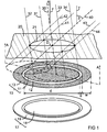
- FIG. 1 shows an arrangement of an aperture, a filter region and a sensor region in a perspective view.
- the filter region 10 comprises a central filter region 11 and a peripheral filter region 13, which are separated by a gap 12 in between.
- the filter region 10 is arranged on or above the sensor region 17, which is provided for spatially individual measurements using a central sensor region 18 and a peripheral sensor region 19.
- a shielding component 20 comprising an aperture 21 is arranged above the filter region 10, so that the aperture 21 is placed above the central filter region 11.
- Figure 1 indicates the diameter D of the aperture 21, the diameter d of the central filter region 11, the width g of the gap 12 between the central filter region 11 and the peripheral filter region 13, and the width w of the peripheral filter region 13.
- the boundaries of the aperture 21, the central filter region 11 and the peripheral filter region 13 may be circular, for instance. In particular, the boundaries of the central filter region 11 and the peripheral filter region 13 may be concentric circles.
- Figure 1 shows two incident central rays 30, 40, which pass the center of the aperture 21, and their angles of incidence ⁇ and ⁇ with respect to the vertical direction v, which is normal to the plane of the filter region 10.
- the angle of incidence ⁇ of the central ray 30 is smaller than the angle of incidence ⁇ of the central ray 40, by way of example.
- Four peripheral rays 31, 32, 33, 34, 41, 42, 43, 44, which pass four selected points at the edge of the aperture 21, are shown for each central ray 30, 40.
- the projections of the area of the aperture 21 onto the filter region 10 in the directions of the central rays 30, 40 are indicated by broken elliptical contours.
- Figure 2 is a schematical cross section of a filter sensor device comprising the elements shown in Figure 1 .
- the line of section is indicated in Figure 1 with letter A.
- the elements of Figure 2 that are similar to corresponding elements of Figure 1 are designated with the same reference numerals.
- Figure 2 shows the height h of the aperture 21 above the filter region 10, i. e. the distance between the plane of the filter region 10 and the shielding component 20.
- the filter sensor device shown in Figure 2 may include a body 14, which may especially comprise semiconductor material.
- An integrated circuit 15 may be provided in the body 14 for the operation of the sensor, especially for the performance and/or the evaluation of the measurements.
- Components of the integrated circuit 15 may be semiconductor devices.
- Electric interconnections 16 like a wiring, for instance, may be provided between the integrated circuit 15 and the central and peripheral sensor regions 18, 19, corresponding to the central filter region 11 and the peripheral filter region 13, respectively.
- the central and peripheral sensor regions 18, 19 are schematically represented adjacent to the filter region 10. They may instead be arranged at a distance from the filter region 10.
- the central and peripheral sensor regions 18, 19 may especially form part of the integrated circuit 15.
- Figure 2 shows two incident central rays 1, 2, which pass the center of the aperture 21.
- Ray 1 is perpendicular to the plane of the filter region 10 and hence impinges on the center of the central filter region 11.
- Rays 3 and 4 define limit paths from opposite points at the edge of the aperture 21 to the farthest points at the boundary of the central filter region 11.
- the angles of incidence ⁇ 3 and ⁇ 4 of rays 3 and 4 are equal because of the symmetry of their directions with respect to ray 1. These angles of incidence ⁇ 3 and ⁇ 4 are maximal for the central filter region 11.
- Figure 2 shows the direction of ray 2 inclined with respect to the normal to the plane of the filter region 10.
- the angle of incidence ⁇ > 0 of ray 2 is sufficiently large to make ray 2 impinge on the peripheral filter region 13.
- Its target point is at equal distances from the concentric circles defining the inner and outer boundaries of the annular peripheral filter region 13 in this embodiment.
- Ray 5 at the angle of incidence ⁇ 5 defines the limit path from one of the points at the edge of the aperture 21 to the nearest target point at the inner boundary of the peripheral filter region 13.
- Ray 6 at the angle of incidence ⁇ 6 defines the limit path from the opposite point at the edge of the aperture 21 to the farthest point at the outer boundary of the peripheral filter region 13.
- the rays 2, 5 and 6 intersect between the aperture 21 and the peripheral filter region 13.
- ⁇ 1 and ⁇ 2 are the maximal deviations from the angle of incidence ⁇ of ray 2.
- the central filter region 11 can be optimized for normal incidence (i. e. angle of incidence being equal to 0°).
- the peripheral filter region 13 can simultaneously be optimized for an angle of incidence ⁇ that can be suitably selected different from zero. Examination of the wavelength shift versus angle of incidence shows the IR (infrared) cut-off wavelength of an IR filter to follow a quadratic relation. As an example, if the transition point (1 ⁇ 2 power point) of the IR filter characteristic is assumed to be at about 665 nm for normal incident light, the IR filter in the central filter region 11 may be designed with a 665 nm transition point.
- the filter response is shifted to counteract the shift induced by the non-zero angle of incidence.
- the filter of the peripheral filter region 13 thus adjusted will transition at about 665 nm as desired for light impinging at an angle of incidence of 30°.
- Figures 1 and 2 show an embodiment comprising two separate filter regions 11, 13.
- the filter region 10 may comprise more than two separate filter regions.
- the separate filter regions can be arranged in different suitable ways.
- the filter region 10 may comprise a plurality of concentric annular filter regions, for example.
- the use of a small aperture 21 allows to limit the ranges of suitable angles of incidence, which are confined by minimal and maximal angles, like ⁇ 5 and ⁇ 6 in the above example.
- the filter arrangement may comprise infrared cut-off filters as described above. Instead or additionally, filter devices may employ color filters.
- Figure 3 is a top view in the direction indicated in Figure 2 by the arrow pointing downwards.
- Figure 3 depicts a typical array of color filters, which may correspond to an arrangement of individual sensor regions.
- the color filters may comprise different filter types, which may especially include absorptive organic filters and/or interference filters, for instance.
- Figure 3 shows an array comprising four types of partial areas of the filter region 10, by way of example. Each of the partial areas may be clear, a red filter, a blue filter or a green filter, for instance.
- the filter region 10 is divided into a plurality of circular sectors that do not overlap, and the partial areas are each arranged within one of the sectors.
- each color filter could be an interference filter that filters a particular color and blocks infrared radiation.
- RGBC filters an X, Y or Z tri-stimulus filter, which is known per se, can be employed.
- the clear filter may typically embody an IR cut filter to reject IR light. If the segmented array according to Figure 3 is used, each of the filters in the peripheral filter region 13 may be shifted in terms of its design as described above, so as to provide the proper transition wavelengths for the particular nominal angle of incidence relevant to that filter region.
- Figure 4 shows an arrangement according to Figure 1 for a further embodiment. Elements of the embodiment according to Figure 4 that are similar to corresponding elements of the embodiment according to Figure 1 are designated with the same reference numerals.
- the embodiment according to Figure 4 comprises a central aperture 21 and a peripheral aperture 23 with an intermediate portion 22 of the shielding component 20 separating the apertures 21, 23.
- the peripheral aperture 23 may be an annular aperture, for instance. It is added to provide additional light gathering area for the peripheral filter region 13.
- the diameter D of the central aperture 21 is smaller than the diameter d of the central filter region 11.
- the width G of the intermediate portion 22 of the shielding component 20 between the apertures 21, 23 is larger than the width W of the peripheral aperture 23.
- the diameter of the inner boundary of the peripheral aperture 23, which is D + 2G, is greater than the diameter of the outer boundary of the peripheral filter region 13, which is d + 2g + 2w.
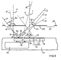
- Figure 5 is a schematical cross section of a filter device comprising elements shown in Figures 2 and 4 .
- the line of section is indicated in Figure 4 with letter B.
- the elements of Figure 5 that are similar to corresponding elements of Figures 2 and 4 are designated with the same reference numerals.
- the arrangement of the rays 2*, 5* and 6* with respect to the peripheral aperture 23 corresponds to the arrangement of the rays 2, 5 and 6 with respect to the central aperture 21.
- the arrangement of the peripheral filter region 13 and the peripheral aperture 23 is provided for a range of angles of incidence from ⁇ 5* to ⁇ 6* .
- the described arrangement of an aperture and a filter region comprising separate subregions has the advantage of reducing errors caused by different angles of incidence, in particular errors that are due to a shift of the transition wavelengths in interference filters.
- Different sensor regions may be employed for individual measurements using different filter characteristics.
- the division into different filter subregions allows to optimize the filters for either perpendicular or inclined incidence.
Landscapes
- Physics & Mathematics (AREA)
- Spectroscopy & Molecular Physics (AREA)
- General Physics & Mathematics (AREA)
- Optics & Photonics (AREA)
- Health & Medical Sciences (AREA)
- Toxicology (AREA)
- Photometry And Measurement Of Optical Pulse Characteristics (AREA)
- Engineering & Computer Science (AREA)
- Multimedia (AREA)
- Signal Processing (AREA)
- Solid State Image Pick-Up Elements (AREA)
Abstract
Description
- Optical sensor devices comprise sensor elements like photodiodes. Filters are placed above the sensor elements for the purpose of selecting spectral ranges. Optical interference filters are formed by successive layers of different optical materials of distinct refractive indexes. The spectral response, which is represented by the wavelength filter curve, can be adjusted by controlling the thickness of the filter layers. Such interference filters are rather sensitive to the angle of incidence. The transition wavelength of the filter tends to shift to progressively shorter wavelengths with increasing angle of incidence. Hence the color measurement depends on the angle of incidence. This effect may also adversely affect the computation of derived quantities like color temperature.
-
WO 2016/005097 A1 discloses an optoelectronic package with lens assembly comprising a lens having an upper surface, a lateral surface surrounding the lens, and a bottom surface. An optoelectronic component is arranged at or near the bottom surface, and an aperture is arranged at the upper surface, so that the lens is arranged between the optoelectronic component and the aperture. Widths of the lens that are defined in a specified lateral direction decrease from a maximal width at or near the bottom surface to a non-vanishing minimal width at the upper surface. The entire lens may be tapered. - It is an object of the present invention to improve the accuracy of optical interference filter-based sensors. This object is achieved with the arrangement of an aperture and a filter region according to claim 1 and with the filter sensor device according to
claim 10. Embodiments derive from the dependent claims. - The arrangement of an aperture and a filter region for sensor devices comprises a filter region provided to filter electromagnetic radiation, a shielding component provided to inhibit propagation of electromagnetic radiation, and an aperture of the shielding component. The filter region comprises a central filter region and a peripheral filter region, which are separate from one another and provided with differently designed filters for individual sensor regions. The aperture is arranged above the central filter region.
- In embodiments of the arrangement, the peripheral filter region surrounds the central filter region at a distance from the central filter region. The central filter region and the peripheral filter region may be symmetrical with respect to rotations. In particular, they may be limited by regular polygons.
- In further embodiments of the arrangement, the central filter region has an infrared cut-off wavelength for normal incidence, and the peripheral filter region has a different infrared cut-off wavelength for normal incidence. In particular, the cut-off wavelength for normal incidence onto the central filter region may be the same as the cut-off wavelength for inclined incidence at a selected angle of incidence onto the peripheral filter region.
- Further embodiments of the arrangement comprise a further aperture of the shielding component, the aperture and the further aperture being separated from one another by an intermediate portion of the shielding component, the further aperture surrounding the aperture. The aperture and the further aperture may be symmetrical with respect to rotations. In particular, they may be limited by regular polygons.
- In further embodiments of the arrangement, at least one of the central filter region and the peripheral filter region is divided into partial areas each of which is clear or provided with a filter selected from the group consisting of red filter, green filter, blue filter and infrared filter. In particular, the partial areas may each be arranged within one of a plurality of circular sectors of the filter region that do not overlap.
- The filter sensor device comprises a body, an integrated circuit in the body, a sensor region, a filter region provided to filter electromagnetic radiation, the filter region being arranged above the sensor region, a shielding component provided to inhibit propagation of electromagnetic radiation, and an aperture of the shielding component. The filter region comprises a central filter region and a separate peripheral filter region, which are provided for individual measurements in a central sensor region and a peripheral sensor region. The aperture is arranged above the central filter region. The central filter region and the peripheral filter region may be symmetrical with respect to rotations, and their areas may in particular be limited by regular polygons.
- Embodiments of the filter sensor device comprise a further aperture of the shielding component, the aperture and the further aperture being separated from one another by an intermediate portion of the shielding component, the further aperture surrounding the aperture.
- In further embodiments of the filter sensor device, the body comprises a semiconductor material, and components of the integrated circuit and the sensor region are formed in the semiconductor material.
- In further embodiments of the filter sensor device, the central filter region has an infrared cut-off wavelength for normal incidence, and the peripheral filter region has a different infrared cut-off wavelength for normal incidence.
- In further embodiments of the filter sensor device, at least one of the central filter region and the peripheral filter region is divided into partial areas each of which is clear or provided with a filter selected from the group consisting of red filter, green filter, blue filter and infrared filter.
- The following is a more detailed description of the arrangement of an aperture and a filter region and the filter sensor device with reference to the accompanying figures.
- Figure 1
- shows an arrangement of an aperture, a filter region and a sensor region.
- Figure 2
- shows the cross section indicated in
Figure 1 . - Figure 3
- shows an arrangement of partial areas of the filter region in a top view.
- Figure 4
- shows a further arrangement of an aperture and a filter region.
- Figure 5
- shows the cross section indicated in
Figure 4 . -
Figure 1 shows an arrangement of an aperture, a filter region and a sensor region in a perspective view. Thefilter region 10 comprises acentral filter region 11 and aperipheral filter region 13, which are separated by agap 12 in between. Thefilter region 10 is arranged on or above thesensor region 17, which is provided for spatially individual measurements using acentral sensor region 18 and aperipheral sensor region 19. Ashielding component 20 comprising anaperture 21 is arranged above thefilter region 10, so that theaperture 21 is placed above thecentral filter region 11. -
Figure 1 indicates the diameter D of theaperture 21, the diameter d of thecentral filter region 11, the width g of thegap 12 between thecentral filter region 11 and theperipheral filter region 13, and the width w of theperipheral filter region 13. The boundaries of theaperture 21, thecentral filter region 11 and theperipheral filter region 13 may be circular, for instance. In particular, the boundaries of thecentral filter region 11 and theperipheral filter region 13 may be concentric circles. -
Figure 1 shows two incidentcentral rays 30, 40, which pass the center of theaperture 21, and their angles of incidence α and β with respect to the vertical direction v, which is normal to the plane of thefilter region 10. The angle of incidence α of thecentral ray 30 is smaller than the angle of incidence β of the central ray 40, by way of example. Fourperipheral rays aperture 21, are shown for eachcentral ray 30, 40. The projections of the area of theaperture 21 onto thefilter region 10 in the directions of thecentral rays 30, 40 are indicated by broken elliptical contours. -
Figure 2 is a schematical cross section of a filter sensor device comprising the elements shown inFigure 1 . The line of section is indicated inFigure 1 with letter A. The elements ofFigure 2 that are similar to corresponding elements ofFigure 1 are designated with the same reference numerals. Further to the dimensions indicated inFigure 1 ,Figure 2 shows the height h of theaperture 21 above thefilter region 10, i. e. the distance between the plane of thefilter region 10 and theshielding component 20. - The filter sensor device shown in
Figure 2 may include abody 14, which may especially comprise semiconductor material. Anintegrated circuit 15 may be provided in thebody 14 for the operation of the sensor, especially for the performance and/or the evaluation of the measurements. Components of theintegrated circuit 15 may be semiconductor devices.Electric interconnections 16 like a wiring, for instance, may be provided between theintegrated circuit 15 and the central andperipheral sensor regions central filter region 11 and theperipheral filter region 13, respectively. - In
Figure 2 , the central andperipheral sensor regions filter region 10. They may instead be arranged at a distance from thefilter region 10. The central andperipheral sensor regions integrated circuit 15. -
Figure 2 shows two incidentcentral rays 1, 2, which pass the center of theaperture 21. Ray 1 is perpendicular to the plane of thefilter region 10 and hence impinges on the center of thecentral filter region 11.Rays 3 and 4 define limit paths from opposite points at the edge of theaperture 21 to the farthest points at the boundary of thecentral filter region 11. The angles of incidence θ3 and θ4 ofrays 3 and 4 are equal because of the symmetry of their directions with respect to ray 1. These angles of incidence θ3 and θ4 are maximal for thecentral filter region 11. -
Figure 2 shows the direction ofray 2 inclined with respect to the normal to the plane of thefilter region 10. The angle of incidence θ > 0 ofray 2 is sufficiently large to makeray 2 impinge on theperipheral filter region 13. Its target point is at equal distances from the concentric circles defining the inner and outer boundaries of the annularperipheral filter region 13 in this embodiment.Ray 5 at the angle of incidence θ5 defines the limit path from one of the points at the edge of theaperture 21 to the nearest target point at the inner boundary of theperipheral filter region 13.Ray 6 at the angle of incidence θ6 defines the limit path from the opposite point at the edge of theaperture 21 to the farthest point at the outer boundary of theperipheral filter region 13. Therays aperture 21 and theperipheral filter region 13. θ1 and θ2 are the maximal deviations from the angle of incidence θ ofray 2. The following equations for θ1 and θ2 are read fromFigure 2 : θk = (-1) k { arctan [ tan θ + (-1) k (w + D) / (2h)] - θ }, where k is either 1 or 2, and tan θ = (½ w + q + ½ d) /h. In this embodiment theperipheral filter region 13 is arranged for angles of incidence in the range from θ5 = θ - θ1 to θ6 = θ + θ2. - The
central filter region 11 can be optimized for normal incidence (i. e. angle of incidence being equal to 0°). Theperipheral filter region 13 can simultaneously be optimized for an angle of incidence θ that can be suitably selected different from zero. Examination of the wavelength shift versus angle of incidence shows the IR (infrared) cut-off wavelength of an IR filter to follow a quadratic relation. As an example, if the transition point (½ power point) of the IR filter characteristic is assumed to be at about 665 nm for normal incident light, the IR filter in thecentral filter region 11 may be designed with a 665 nm transition point. If the transition point is at about 635 nm for rays incident at an angle of 30°, for instance, the filter of theperipheral filter region 13 is designed to transition at the wavelength 665 nm + 30 nm = 695 nm for rays incident in the normal direction (zero angle of incidence). Thus the filter response is shifted to counteract the shift induced by the non-zero angle of incidence. - As a result, the filter of the
peripheral filter region 13 thus adjusted will transition at about 665 nm as desired for light impinging at an angle of incidence of 30°. This is only one example for the filter design, which can be adapted to the requirements of individual embodiments of a filter sensor device. In this way sections of the filter region can be designed such that their characteristics are similar and/or appropriate although each section is illuminated with rays impinging at angles belonging to different ranges. -
Figures 1 and2 show an embodiment comprising twoseparate filter regions filter region 10 may comprise more than two separate filter regions. The separate filter regions can be arranged in different suitable ways. In particular, thefilter region 10 may comprise a plurality of concentric annular filter regions, for example. The use of asmall aperture 21 allows to limit the ranges of suitable angles of incidence, which are confined by minimal and maximal angles, like θ5 and θ6 in the above example. The filter arrangement may comprise infrared cut-off filters as described above. Instead or additionally, filter devices may employ color filters. -
Figure 3 is a top view in the direction indicated inFigure 2 by the arrow pointing downwards.Figure 3 depicts a typical array of color filters, which may correspond to an arrangement of individual sensor regions. The color filters may comprise different filter types, which may especially include absorptive organic filters and/or interference filters, for instance.Figure 3 shows an array comprising four types of partial areas of thefilter region 10, by way of example. Each of the partial areas may be clear, a red filter, a blue filter or a green filter, for instance. In the example ofFigure 3 , thefilter region 10 is divided into a plurality of circular sectors that do not overlap, and the partial areas are each arranged within one of the sectors. - In yet another embodiment each color filter could be an interference filter that filters a particular color and blocks infrared radiation. Instead of RGBC filters, an X, Y or Z tri-stimulus filter, which is known per se, can be employed. The clear filter may typically embody an IR cut filter to reject IR light. If the segmented array according to
Figure 3 is used, each of the filters in theperipheral filter region 13 may be shifted in terms of its design as described above, so as to provide the proper transition wavelengths for the particular nominal angle of incidence relevant to that filter region. -
Figure 4 shows an arrangement according toFigure 1 for a further embodiment. Elements of the embodiment according toFigure 4 that are similar to corresponding elements of the embodiment according toFigure 1 are designated with the same reference numerals. The embodiment according toFigure 4 comprises acentral aperture 21 and aperipheral aperture 23 with anintermediate portion 22 of theshielding component 20 separating theapertures peripheral aperture 23 may be an annular aperture, for instance. It is added to provide additional light gathering area for theperipheral filter region 13. - In the embodiment according to
Figure 4 , the diameter D of thecentral aperture 21 is smaller than the diameter d of thecentral filter region 11. The width G of theintermediate portion 22 of theshielding component 20 between theapertures peripheral aperture 23. The diameter of the inner boundary of theperipheral aperture 23, which is D + 2G, is greater than the diameter of the outer boundary of theperipheral filter region 13, which is d + 2g + 2w. These dimensions may be adapted to the requirements of individual embodiments, so that the relations between the dimensions may differ from the embodiment according toFigure 4 . -
Figure 5 is a schematical cross section of a filter device comprising elements shown inFigures 2 and4 . The line of section is indicated inFigure 4 with letter B. The elements ofFigure 5 that are similar to corresponding elements ofFigures 2 and4 are designated with the same reference numerals. The arrangement of therays 2*, 5* and 6* with respect to theperipheral aperture 23 corresponds to the arrangement of therays central aperture 21. The respective angles of incidence are θ*, θ5* = θ* - θ1* and θ6* = θ* + θ2*. In the embodiment according toFigure 5 , the arrangement of theperipheral filter region 13 and theperipheral aperture 23 is provided for a range of angles of incidence from θ5* to θ6*. - The described arrangement of an aperture and a filter region comprising separate subregions has the advantage of reducing errors caused by different angles of incidence, in particular errors that are due to a shift of the transition wavelengths in interference filters. Different sensor regions may be employed for individual measurements using different filter characteristics. The division into different filter subregions allows to optimize the filters for either perpendicular or inclined incidence.
-
- 1
- perpendicular central ray
- 2
- inclined central ray
- 3
- ray from aperture edge to farthest target on center
- 4
- ray from aperture edge to farthest target on center
- 5
- ray from aperture edge to nearest target on periphery
- 6
- ray from aperture edge to farthest target on periphery
- 1*
- perpendicular straight line
- 2*
- further inclined central ray
- 5*
- shortest ray from peripheral aperture to filter region
- 6*
- shortest ray from outermost aperture edge to the gap
- 10
- filter region
- 11
- central filter region
- 12
- gap between filter regions
- 13
- peripheral filter region
- 14
- body
- 15
- integrated circuit
- 16
- electric interconnection
- 17
- sensor region
- 18
- central sensor region
- 19
- peripheral sensor region
- 20
- shielding component
- 21
- central aperture
- 22
- intermediate portion between apertures
- 23
- peripheral aperture
- 30
- central ray
- 31
- first peripheral ray
- 32
- second peripheral ray
- 33
- third peripheral ray
- 34
- fourth peripheral ray
- 40
- further central ray
- 41
- first further peripheral ray
- 42
- second further peripheral ray
- 43
- third further peripheral ray
- 44
- fourth further peripheral ray
- D
- diameter of central aperture
- d
- diameter of central filter region
- G
- width of intermediate portion between apertures
- g
- width of gap between filter regions
- h
- height of the aperture above the filter region
- v
- vertical direction
- W
- width of peripheral aperture
- w
- width of peripheral filter region
- α
- angle of incidence
- β
- further angle of incidence
- θ
- angle of incidence of
ray 2 - θ1
- first angle of deviation
- θ2
- second angle of deviation
- θ3
- angle of incidence of ray 3
- θ4
- angle of incidence of
ray 4 - θ5
- angle of incidence of
ray 5 - θ6
- angle of incidence of
ray 6 - θ*
- angle of incidence of
ray 2* - θ1*
- further first angle of deviation
- θ2*
- further second angle of deviation
- θ5*
- angle of incidence of
ray 5* - θ6*
- angle of incidence of
ray 6*
Claims (15)
- An arrangement of an aperture and a filter region for a sensor device, comprising:- a filter region (10) provided to filter electromagnetic radiation,- a shielding component (20) provided to inhibit propagation of electromagnetic radiation, and- an aperture (21) of the shielding component (20), the aperture (21) being arranged above the filter region (10),characterized in that- the filter region (10) comprises a central filter region (11) and a peripheral filter region (13), which are separate from one another,- the aperture (21) is arranged above the central filter region (11), and- the central filter region (11) and the peripheral filter region (13) are provided with differently designed filters for individual sensor regions (18, 19).
- The arrangement according to claim 1, wherein
the peripheral filter region (13) completely surrounds the central filter region (11) at a distance from the central filter region (11). - The arrangement according to claim 1 or 2, wherein
the central filter region (11) has an infrared cut-off wavelength for normal incidence, and the peripheral filter region (13) has a further infrared cut-off wavelength for normal incidence, the infrared cut-off wavelength and the further infrared cut-off wavelength being different from one another. - The arrangement according to claim 3, wherein
the cut-off wavelength for normal incidence onto the central filter region (11) is the same as the cut-off wavelength for inclined incidence at a selected angle of incidence (θ) onto the peripheral filter region (13). - The arrangement according to one of claims 1 to 4, further comprising:a further aperture (23) of the shielding component (20),the aperture (21) and the further aperture (23) being separated from one another by an intermediate portion (22) of the shielding component (20), the further aperture (23) surrounding the aperture (21).
- The arrangement according to claim 5, wherein
the aperture (21) and the further aperture (23) are symmetrical with respect to rotations. - The arrangement according to one of claims 1 to 6,
wherein
the filter region (10) is symmetrical with respect to rotations. - The arrangement according to claim 7, further comprising:sectors of the filter region (10), at least one of the central filter region (11) and the peripheral filter region (13) being divided into partial areas each arranged within one of the sectors, the partial areas being provided with different types of filters.
- The arrangement according to claim 8, wherein
the partial areas are clear or provided with a filter selected from the group consisting of red filter, green filter, blue filter and infrared filter. - A filter sensor device, comprising:- a body (14),- an integrated circuit (15) in the body (14),- a sensor region (17),- a filter region (10) provided to filter electromagnetic radiation, the filter region (10) being arranged above the sensor region (17),- a shielding component (20) provided to inhibit propagation of electromagnetic radiation, and- an aperture (21) of the shielding component (20), the aperture (21) being arranged above the filter region (10),characterized in that- the filter region (10) comprises a central filter region (11) and a peripheral filter region (13), which are separate from one another,- the aperture (21) is arranged above the central filter region (11), and- the central filter region (11) and the peripheral filter region (13) are provided for individual measurements in a central sensor region (18) and a peripheral sensor region (19) of the sensor region (17).
- The filter sensor device according to claim 10, wherein the central filter region (11) and the peripheral filter region (13) are symmetrical with respect to rotations.
- The filter sensor device according to claim 10 or 11, further comprising:a further aperture (23) of the shielding component (20), the aperture (21) and the further aperture (23) being separated from one another by an intermediate portion (22) of the shielding component (20), and the further aperture (23) surrounding the aperture (21).
- The filter sensor device according to one of claims 10 to 12, further comprising:the body (14) comprising a semiconductor material, andcomponents of the integrated circuit (15) and the sensor region (17) being formed in the semiconductor material.
- The filter sensor device according to one of claims 10 to 13, wherein
the central filter region (11) has an infrared cut-off wavelength for normal incidence, and
the peripheral filter region (13) has a further infrared cut-off wavelength for normal incidence,
the infrared cut-off wavelength and the further infrared cut-off wavelength being different from one another. - The filter sensor device according to one of claims 10 to 14, wherein
at least one of the central filter region (11) and the peripheral filter region (13) is divided into partial areas that are clear or provided with a filter selected from the group consisting of red filter, green filter, blue filter and infrared filter.
Priority Applications (1)
| Application Number | Priority Date | Filing Date | Title |
|---|---|---|---|
| US15/586,192 US10423849B2 (en) | 2016-05-04 | 2017-05-03 | Arrangement of an aperture and a filter region for a filter sensor device and filter sensor device |
Applications Claiming Priority (1)
| Application Number | Priority Date | Filing Date | Title |
|---|---|---|---|
| US201662331674P | 2016-05-04 | 2016-05-04 |
Publications (2)
| Publication Number | Publication Date |
|---|---|
| EP3242114A1 true EP3242114A1 (en) | 2017-11-08 |
| EP3242114B1 EP3242114B1 (en) | 2019-05-01 |
Family
ID=56131378
Family Applications (1)
| Application Number | Title | Priority Date | Filing Date |
|---|---|---|---|
| EP16174001.4A Active EP3242114B1 (en) | 2016-05-04 | 2016-06-10 | Arrangement of an aperture and a filter region for a filter sensor device and filter sensor device |
Country Status (2)
| Country | Link |
|---|---|
| US (1) | US10423849B2 (en) |
| EP (1) | EP3242114B1 (en) |
Cited By (2)
| Publication number | Priority date | Publication date | Assignee | Title |
|---|---|---|---|---|
| US20190162885A1 (en) * | 2017-11-30 | 2019-05-30 | Qualcomm Incorporated | Optical bandpass filter design |
| WO2024156637A1 (en) | 2023-01-23 | 2024-08-02 | Trinamix Gmbh | Method for arranging an optical measurement device |
Families Citing this family (3)
| Publication number | Priority date | Publication date | Assignee | Title |
|---|---|---|---|---|
| JP2022002229A (en) * | 2018-09-05 | 2022-01-06 | ソニーセミコンダクタソリューションズ株式会社 | Image pickup device and image sensor |
| DE102020102247A1 (en) * | 2020-01-30 | 2021-08-05 | Sick Ag | Optoelectronic sensor and method for detecting objects |
| DE102020202824A1 (en) | 2020-03-05 | 2021-09-09 | OSRAM Opto Semiconductors Gesellschaft mit beschränkter Haftung | SENSOR DEVICE USING THE ANGLE DEPENDENCE OF A DICHROITIC FILTER |
Citations (8)
| Publication number | Priority date | Publication date | Assignee | Title |
|---|---|---|---|---|
| US20050146634A1 (en) * | 2003-12-31 | 2005-07-07 | Silverstein D. A. | Cameras, optical systems, imaging methods, and optical filter configuration methods |
| WO2010081556A1 (en) * | 2009-01-16 | 2010-07-22 | Iplink Limited | Improving the depth of field in an imaging system |
| US20100265375A1 (en) * | 2009-04-15 | 2010-10-21 | Sony Corporation | Solid-state imaging device and electronic apparatus |
| US20130215238A1 (en) * | 2012-02-21 | 2013-08-22 | Sony Corporation | Imaging apparatus and image sensor array |
| US9071721B1 (en) * | 2012-12-21 | 2015-06-30 | Google Inc. | Camera architecture having a repositionable color filter array |
| US20150260888A1 (en) * | 2012-11-30 | 2015-09-17 | Asahi Glass Company, Limited | Near-infrared cut filter |
| US9217671B2 (en) * | 2009-09-01 | 2015-12-22 | Koninklijke Philips N.V. | High spectral resolution color sensor using non-dispersive elements |
| WO2016005097A1 (en) | 2014-07-09 | 2016-01-14 | Ams Ag | Lens assembly, optoelectronic package and method of producing an optoelectronic package with lens assembly |
Family Cites Families (2)
| Publication number | Priority date | Publication date | Assignee | Title |
|---|---|---|---|---|
| JP4078551B2 (en) * | 2003-08-08 | 2008-04-23 | ミネベア株式会社 | Color wheel, manufacturing method thereof, spectroscopic device including the same, and image display device |
| US7881603B2 (en) * | 2008-09-26 | 2011-02-01 | Apple Inc. | Dichroic aperture for electronic imaging device |
-
2016
- 2016-06-10 EP EP16174001.4A patent/EP3242114B1/en active Active
-
2017
- 2017-05-03 US US15/586,192 patent/US10423849B2/en active Active
Patent Citations (8)
| Publication number | Priority date | Publication date | Assignee | Title |
|---|---|---|---|---|
| US20050146634A1 (en) * | 2003-12-31 | 2005-07-07 | Silverstein D. A. | Cameras, optical systems, imaging methods, and optical filter configuration methods |
| WO2010081556A1 (en) * | 2009-01-16 | 2010-07-22 | Iplink Limited | Improving the depth of field in an imaging system |
| US20100265375A1 (en) * | 2009-04-15 | 2010-10-21 | Sony Corporation | Solid-state imaging device and electronic apparatus |
| US9217671B2 (en) * | 2009-09-01 | 2015-12-22 | Koninklijke Philips N.V. | High spectral resolution color sensor using non-dispersive elements |
| US20130215238A1 (en) * | 2012-02-21 | 2013-08-22 | Sony Corporation | Imaging apparatus and image sensor array |
| US20150260888A1 (en) * | 2012-11-30 | 2015-09-17 | Asahi Glass Company, Limited | Near-infrared cut filter |
| US9071721B1 (en) * | 2012-12-21 | 2015-06-30 | Google Inc. | Camera architecture having a repositionable color filter array |
| WO2016005097A1 (en) | 2014-07-09 | 2016-01-14 | Ams Ag | Lens assembly, optoelectronic package and method of producing an optoelectronic package with lens assembly |
Cited By (3)
| Publication number | Priority date | Publication date | Assignee | Title |
|---|---|---|---|---|
| US20190162885A1 (en) * | 2017-11-30 | 2019-05-30 | Qualcomm Incorporated | Optical bandpass filter design |
| WO2019108611A1 (en) * | 2017-11-30 | 2019-06-06 | Qualcomm Incorporated | Optical bandpass filter design |
| WO2024156637A1 (en) | 2023-01-23 | 2024-08-02 | Trinamix Gmbh | Method for arranging an optical measurement device |
Also Published As
| Publication number | Publication date |
|---|---|
| US10423849B2 (en) | 2019-09-24 |
| EP3242114B1 (en) | 2019-05-01 |
| US20170323171A1 (en) | 2017-11-09 |
Similar Documents
| Publication | Publication Date | Title |
|---|---|---|
| US10423849B2 (en) | Arrangement of an aperture and a filter region for a filter sensor device and filter sensor device | |
| KR102053561B1 (en) | Method of manufacturing the light detecting device and the light detecting device | |
| US8780257B2 (en) | Imager device for evaluating distances of elements in an image | |
| CN109520618B (en) | Optical filter and spectrometer | |
| JP6015034B2 (en) | Optical sensor and electronic equipment | |
| US8847162B2 (en) | Infrared detector comprising a package integrating at least one diffraction grating | |
| KR20170095158A (en) | Optical filter array | |
| DE112013002556B4 (en) | spectral sensor | |
| EP2873953A1 (en) | Light sensor arrangement and spectrometer | |
| DE102008011793A1 (en) | multispectral sensor | |
| US11892666B2 (en) | Multispectral sensor response balancing | |
| EP3419053A1 (en) | Optical component with waveguide based filter | |
| US11143554B2 (en) | Multispectral imaging device with array of microlenses | |
| US9958320B2 (en) | Apparatus for selectively transmitting the spectrum of electromagnetic radiation within a predefined wavelength range | |
| US10139339B2 (en) | Colour sensor with angle-selective structures | |
| KR20180090116A (en) | Light filter and Spectrometer comprising the same | |
| US20230030472A1 (en) | Optical sensor | |
| JP2006135320A (en) | Optical color sensor using diffractive elements | |
| CN111164394B (en) | Optical sensing device and method for manufacturing optical sensing device | |
| JP4689971B2 (en) | Manufacturing method of illuminance sensor | |
| WO2021181818A1 (en) | Solid-state imaging element and electronic device | |
| US20210066376A1 (en) | Cmos wavefront sensors | |
| JP6692190B2 (en) | Optical sensor and manufacturing method thereof | |
| KR102618550B1 (en) | Image sensor including meta pattern layer also having light resonance function | |
| JP2017168535A (en) | Optical sensor |
Legal Events
| Date | Code | Title | Description |
|---|---|---|---|
| PUAI | Public reference made under article 153(3) epc to a published international application that has entered the european phase |
Free format text: ORIGINAL CODE: 0009012 |
|
| STAA | Information on the status of an ep patent application or granted ep patent |
Free format text: STATUS: THE APPLICATION HAS BEEN PUBLISHED |
|
| AK | Designated contracting states |
Kind code of ref document: A1 Designated state(s): AL AT BE BG CH CY CZ DE DK EE ES FI FR GB GR HR HU IE IS IT LI LT LU LV MC MK MT NL NO PL PT RO RS SE SI SK SM TR |
|
| AX | Request for extension of the european patent |
Extension state: BA ME |
|
| STAA | Information on the status of an ep patent application or granted ep patent |
Free format text: STATUS: REQUEST FOR EXAMINATION WAS MADE |
|
| 17P | Request for examination filed |
Effective date: 20171215 |
|
| RBV | Designated contracting states (corrected) |
Designated state(s): AL AT BE BG CH CY CZ DE DK EE ES FI FR GB GR HR HU IE IS IT LI LT LU LV MC MK MT NL NO PL PT RO RS SE SI SK SM TR |
|
| STAA | Information on the status of an ep patent application or granted ep patent |
Free format text: STATUS: EXAMINATION IS IN PROGRESS |
|
| 17Q | First examination report despatched |
Effective date: 20180511 |
|
| GRAP | Despatch of communication of intention to grant a patent |
Free format text: ORIGINAL CODE: EPIDOSNIGR1 |
|
| STAA | Information on the status of an ep patent application or granted ep patent |
Free format text: STATUS: GRANT OF PATENT IS INTENDED |
|
| INTG | Intention to grant announced |
Effective date: 20181019 |
|
| RAP1 | Party data changed (applicant data changed or rights of an application transferred) |
Owner name: AMS AG |
|
| GRAS | Grant fee paid |
Free format text: ORIGINAL CODE: EPIDOSNIGR3 |
|
| GRAA | (expected) grant |
Free format text: ORIGINAL CODE: 0009210 |
|
| STAA | Information on the status of an ep patent application or granted ep patent |
Free format text: STATUS: THE PATENT HAS BEEN GRANTED |
|
| AK | Designated contracting states |
Kind code of ref document: B1 Designated state(s): AL AT BE BG CH CY CZ DE DK EE ES FI FR GB GR HR HU IE IS IT LI LT LU LV MC MK MT NL NO PL PT RO RS SE SI SK SM TR |
|
| REG | Reference to a national code |
Ref country code: GB Ref legal event code: FG4D |
|
| REG | Reference to a national code |
Ref country code: CH Ref legal event code: EP Ref country code: AT Ref legal event code: REF Ref document number: 1127575 Country of ref document: AT Kind code of ref document: T Effective date: 20190515 |
|
| REG | Reference to a national code |
Ref country code: DE Ref legal event code: R096 Ref document number: 602016013055 Country of ref document: DE |
|
| REG | Reference to a national code |
Ref country code: IE Ref legal event code: FG4D |
|
| REG | Reference to a national code |
Ref country code: NL Ref legal event code: MP Effective date: 20190501 |
|
| REG | Reference to a national code |
Ref country code: LT Ref legal event code: MG4D |
|
| PG25 | Lapsed in a contracting state [announced via postgrant information from national office to epo] |
Ref country code: ES Free format text: LAPSE BECAUSE OF FAILURE TO SUBMIT A TRANSLATION OF THE DESCRIPTION OR TO PAY THE FEE WITHIN THE PRESCRIBED TIME-LIMIT Effective date: 20190501 Ref country code: HR Free format text: LAPSE BECAUSE OF FAILURE TO SUBMIT A TRANSLATION OF THE DESCRIPTION OR TO PAY THE FEE WITHIN THE PRESCRIBED TIME-LIMIT Effective date: 20190501 Ref country code: NO Free format text: LAPSE BECAUSE OF FAILURE TO SUBMIT A TRANSLATION OF THE DESCRIPTION OR TO PAY THE FEE WITHIN THE PRESCRIBED TIME-LIMIT Effective date: 20190801 Ref country code: AL Free format text: LAPSE BECAUSE OF FAILURE TO SUBMIT A TRANSLATION OF THE DESCRIPTION OR TO PAY THE FEE WITHIN THE PRESCRIBED TIME-LIMIT Effective date: 20190501 Ref country code: SE Free format text: LAPSE BECAUSE OF FAILURE TO SUBMIT A TRANSLATION OF THE DESCRIPTION OR TO PAY THE FEE WITHIN THE PRESCRIBED TIME-LIMIT Effective date: 20190501 Ref country code: PT Free format text: LAPSE BECAUSE OF FAILURE TO SUBMIT A TRANSLATION OF THE DESCRIPTION OR TO PAY THE FEE WITHIN THE PRESCRIBED TIME-LIMIT Effective date: 20190901 Ref country code: FI Free format text: LAPSE BECAUSE OF FAILURE TO SUBMIT A TRANSLATION OF THE DESCRIPTION OR TO PAY THE FEE WITHIN THE PRESCRIBED TIME-LIMIT Effective date: 20190501 Ref country code: LT Free format text: LAPSE BECAUSE OF FAILURE TO SUBMIT A TRANSLATION OF THE DESCRIPTION OR TO PAY THE FEE WITHIN THE PRESCRIBED TIME-LIMIT Effective date: 20190501 Ref country code: NL Free format text: LAPSE BECAUSE OF FAILURE TO SUBMIT A TRANSLATION OF THE DESCRIPTION OR TO PAY THE FEE WITHIN THE PRESCRIBED TIME-LIMIT Effective date: 20190501 |
|
| PG25 | Lapsed in a contracting state [announced via postgrant information from national office to epo] |
Ref country code: GR Free format text: LAPSE BECAUSE OF FAILURE TO SUBMIT A TRANSLATION OF THE DESCRIPTION OR TO PAY THE FEE WITHIN THE PRESCRIBED TIME-LIMIT Effective date: 20190802 Ref country code: RS Free format text: LAPSE BECAUSE OF FAILURE TO SUBMIT A TRANSLATION OF THE DESCRIPTION OR TO PAY THE FEE WITHIN THE PRESCRIBED TIME-LIMIT Effective date: 20190501 Ref country code: BG Free format text: LAPSE BECAUSE OF FAILURE TO SUBMIT A TRANSLATION OF THE DESCRIPTION OR TO PAY THE FEE WITHIN THE PRESCRIBED TIME-LIMIT Effective date: 20190801 Ref country code: LV Free format text: LAPSE BECAUSE OF FAILURE TO SUBMIT A TRANSLATION OF THE DESCRIPTION OR TO PAY THE FEE WITHIN THE PRESCRIBED TIME-LIMIT Effective date: 20190501 |
|
| REG | Reference to a national code |
Ref country code: AT Ref legal event code: MK05 Ref document number: 1127575 Country of ref document: AT Kind code of ref document: T Effective date: 20190501 |
|
| PG25 | Lapsed in a contracting state [announced via postgrant information from national office to epo] |
Ref country code: IS Free format text: LAPSE BECAUSE OF FAILURE TO SUBMIT A TRANSLATION OF THE DESCRIPTION OR TO PAY THE FEE WITHIN THE PRESCRIBED TIME-LIMIT Effective date: 20190901 |
|
| PG25 | Lapsed in a contracting state [announced via postgrant information from national office to epo] |
Ref country code: DK Free format text: LAPSE BECAUSE OF FAILURE TO SUBMIT A TRANSLATION OF THE DESCRIPTION OR TO PAY THE FEE WITHIN THE PRESCRIBED TIME-LIMIT Effective date: 20190501 Ref country code: AT Free format text: LAPSE BECAUSE OF FAILURE TO SUBMIT A TRANSLATION OF THE DESCRIPTION OR TO PAY THE FEE WITHIN THE PRESCRIBED TIME-LIMIT Effective date: 20190501 Ref country code: EE Free format text: LAPSE BECAUSE OF FAILURE TO SUBMIT A TRANSLATION OF THE DESCRIPTION OR TO PAY THE FEE WITHIN THE PRESCRIBED TIME-LIMIT Effective date: 20190501 Ref country code: MC Free format text: LAPSE BECAUSE OF FAILURE TO SUBMIT A TRANSLATION OF THE DESCRIPTION OR TO PAY THE FEE WITHIN THE PRESCRIBED TIME-LIMIT Effective date: 20190501 Ref country code: CZ Free format text: LAPSE BECAUSE OF FAILURE TO SUBMIT A TRANSLATION OF THE DESCRIPTION OR TO PAY THE FEE WITHIN THE PRESCRIBED TIME-LIMIT Effective date: 20190501 Ref country code: RO Free format text: LAPSE BECAUSE OF FAILURE TO SUBMIT A TRANSLATION OF THE DESCRIPTION OR TO PAY THE FEE WITHIN THE PRESCRIBED TIME-LIMIT Effective date: 20190501 Ref country code: SK Free format text: LAPSE BECAUSE OF FAILURE TO SUBMIT A TRANSLATION OF THE DESCRIPTION OR TO PAY THE FEE WITHIN THE PRESCRIBED TIME-LIMIT Effective date: 20190501 |
|
| REG | Reference to a national code |
Ref country code: CH Ref legal event code: PL |
|
| REG | Reference to a national code |
Ref country code: DE Ref legal event code: R097 Ref document number: 602016013055 Country of ref document: DE |
|
| PG25 | Lapsed in a contracting state [announced via postgrant information from national office to epo] |
Ref country code: IT Free format text: LAPSE BECAUSE OF FAILURE TO SUBMIT A TRANSLATION OF THE DESCRIPTION OR TO PAY THE FEE WITHIN THE PRESCRIBED TIME-LIMIT Effective date: 20190501 Ref country code: SM Free format text: LAPSE BECAUSE OF FAILURE TO SUBMIT A TRANSLATION OF THE DESCRIPTION OR TO PAY THE FEE WITHIN THE PRESCRIBED TIME-LIMIT Effective date: 20190501 |
|
| PLBE | No opposition filed within time limit |
Free format text: ORIGINAL CODE: 0009261 |
|
| STAA | Information on the status of an ep patent application or granted ep patent |
Free format text: STATUS: NO OPPOSITION FILED WITHIN TIME LIMIT |
|
| REG | Reference to a national code |
Ref country code: BE Ref legal event code: MM Effective date: 20190630 |
|
| PG25 | Lapsed in a contracting state [announced via postgrant information from national office to epo] |
Ref country code: TR Free format text: LAPSE BECAUSE OF FAILURE TO SUBMIT A TRANSLATION OF THE DESCRIPTION OR TO PAY THE FEE WITHIN THE PRESCRIBED TIME-LIMIT Effective date: 20190501 |
|
| 26N | No opposition filed |
Effective date: 20200204 |
|
| PG25 | Lapsed in a contracting state [announced via postgrant information from national office to epo] |
Ref country code: PL Free format text: LAPSE BECAUSE OF FAILURE TO SUBMIT A TRANSLATION OF THE DESCRIPTION OR TO PAY THE FEE WITHIN THE PRESCRIBED TIME-LIMIT Effective date: 20190501 Ref country code: IE Free format text: LAPSE BECAUSE OF NON-PAYMENT OF DUE FEES Effective date: 20190610 |
|
| PG25 | Lapsed in a contracting state [announced via postgrant information from national office to epo] |
Ref country code: BE Free format text: LAPSE BECAUSE OF NON-PAYMENT OF DUE FEES Effective date: 20190630 Ref country code: SI Free format text: LAPSE BECAUSE OF FAILURE TO SUBMIT A TRANSLATION OF THE DESCRIPTION OR TO PAY THE FEE WITHIN THE PRESCRIBED TIME-LIMIT Effective date: 20190501 Ref country code: LI Free format text: LAPSE BECAUSE OF NON-PAYMENT OF DUE FEES Effective date: 20190630 Ref country code: LU Free format text: LAPSE BECAUSE OF NON-PAYMENT OF DUE FEES Effective date: 20190610 Ref country code: CH Free format text: LAPSE BECAUSE OF NON-PAYMENT OF DUE FEES Effective date: 20190630 |
|
| PG25 | Lapsed in a contracting state [announced via postgrant information from national office to epo] |
Ref country code: CY Free format text: LAPSE BECAUSE OF FAILURE TO SUBMIT A TRANSLATION OF THE DESCRIPTION OR TO PAY THE FEE WITHIN THE PRESCRIBED TIME-LIMIT Effective date: 20190501 |
|
| PG25 | Lapsed in a contracting state [announced via postgrant information from national office to epo] |
Ref country code: MT Free format text: LAPSE BECAUSE OF FAILURE TO SUBMIT A TRANSLATION OF THE DESCRIPTION OR TO PAY THE FEE WITHIN THE PRESCRIBED TIME-LIMIT Effective date: 20190501 Ref country code: HU Free format text: LAPSE BECAUSE OF FAILURE TO SUBMIT A TRANSLATION OF THE DESCRIPTION OR TO PAY THE FEE WITHIN THE PRESCRIBED TIME-LIMIT; INVALID AB INITIO Effective date: 20160610 |
|
| PG25 | Lapsed in a contracting state [announced via postgrant information from national office to epo] |
Ref country code: MK Free format text: LAPSE BECAUSE OF FAILURE TO SUBMIT A TRANSLATION OF THE DESCRIPTION OR TO PAY THE FEE WITHIN THE PRESCRIBED TIME-LIMIT Effective date: 20190501 |
|
| P01 | Opt-out of the competence of the unified patent court (upc) registered |
Effective date: 20230822 |
|
| PGFP | Annual fee paid to national office [announced via postgrant information from national office to epo] |
Ref country code: DE Payment date: 20250618 Year of fee payment: 10 |
|
| PGFP | Annual fee paid to national office [announced via postgrant information from national office to epo] |
Ref country code: GB Payment date: 20250618 Year of fee payment: 10 |
|
| PGFP | Annual fee paid to national office [announced via postgrant information from national office to epo] |
Ref country code: FR Payment date: 20250625 Year of fee payment: 10 |