EP3240306A1 - Multi-device transducer module, apparatus including the transducer module and method of manufacturing the transducer module - Google Patents
Multi-device transducer module, apparatus including the transducer module and method of manufacturing the transducer module Download PDFInfo
- Publication number
- EP3240306A1 EP3240306A1 EP17162651.8A EP17162651A EP3240306A1 EP 3240306 A1 EP3240306 A1 EP 3240306A1 EP 17162651 A EP17162651 A EP 17162651A EP 3240306 A1 EP3240306 A1 EP 3240306A1
- Authority
- EP
- European Patent Office
- Prior art keywords
- substrate
- mems transducer
- package
- integrated circuit
- mems
- Prior art date
- Legal status (The legal status is an assumption and is not a legal conclusion. Google has not performed a legal analysis and makes no representation as to the accuracy of the status listed.)
- Granted
Links
Images



Classifications
-
- H—ELECTRICITY
- H04—ELECTRIC COMMUNICATION TECHNIQUE
- H04R—LOUDSPEAKERS, MICROPHONES, GRAMOPHONE PICK-UPS OR LIKE ACOUSTIC ELECTROMECHANICAL TRANSDUCERS; ELECTRIC HEARING AIDS; PUBLIC ADDRESS SYSTEMS
- H04R19/00—Electrostatic transducers
- H04R19/04—Microphones
-
- B—PERFORMING OPERATIONS; TRANSPORTING
- B06—GENERATING OR TRANSMITTING MECHANICAL VIBRATIONS IN GENERAL
- B06B—METHODS OR APPARATUS FOR GENERATING OR TRANSMITTING MECHANICAL VIBRATIONS OF INFRASONIC, SONIC, OR ULTRASONIC FREQUENCY, e.g. FOR PERFORMING MECHANICAL WORK IN GENERAL
- B06B1/00—Methods or apparatus for generating mechanical vibrations of infrasonic, sonic, or ultrasonic frequency
- B06B1/02—Methods or apparatus for generating mechanical vibrations of infrasonic, sonic, or ultrasonic frequency making use of electrical energy
- B06B1/0292—Electrostatic transducers, e.g. electret-type
-
- B—PERFORMING OPERATIONS; TRANSPORTING
- B81—MICROSTRUCTURAL TECHNOLOGY
- B81B—MICROSTRUCTURAL DEVICES OR SYSTEMS, e.g. MICROMECHANICAL DEVICES
- B81B7/00—Microstructural systems ; Auxiliary parts of microstructural devices or systems
- B81B7/02—Microstructural systems ; Auxiliary parts of microstructural devices or systems containing distinct electrical or optical devices of particular relevance for their function, e.g. microelectro-mechanical systems [MEMS]
-
- B—PERFORMING OPERATIONS; TRANSPORTING
- B81—MICROSTRUCTURAL TECHNOLOGY
- B81B—MICROSTRUCTURAL DEVICES OR SYSTEMS, e.g. MICROMECHANICAL DEVICES
- B81B7/00—Microstructural systems ; Auxiliary parts of microstructural devices or systems
- B81B7/04—Networks or arrays of similar microstructural devices
-
- B—PERFORMING OPERATIONS; TRANSPORTING
- B81—MICROSTRUCTURAL TECHNOLOGY
- B81C—PROCESSES OR APPARATUS SPECIALLY ADAPTED FOR THE MANUFACTURE OR TREATMENT OF MICROSTRUCTURAL DEVICES OR SYSTEMS
- B81C1/00—Manufacture or treatment of devices or systems in or on a substrate
- B81C1/00015—Manufacture or treatment of devices or systems in or on a substrate for manufacturing microsystems
- B81C1/00222—Integrating an electronic processing unit with a micromechanical structure
- B81C1/0023—Packaging together an electronic processing unit die and a micromechanical structure die
-
- H—ELECTRICITY
- H04—ELECTRIC COMMUNICATION TECHNIQUE
- H04R—LOUDSPEAKERS, MICROPHONES, GRAMOPHONE PICK-UPS OR LIKE ACOUSTIC ELECTROMECHANICAL TRANSDUCERS; ELECTRIC HEARING AIDS; PUBLIC ADDRESS SYSTEMS
- H04R1/00—Details of transducers, loudspeakers or microphones
- H04R1/44—Special adaptations for subaqueous use, e.g. for hydrophone
-
- H—ELECTRICITY
- H04—ELECTRIC COMMUNICATION TECHNIQUE
- H04R—LOUDSPEAKERS, MICROPHONES, GRAMOPHONE PICK-UPS OR LIKE ACOUSTIC ELECTROMECHANICAL TRANSDUCERS; ELECTRIC HEARING AIDS; PUBLIC ADDRESS SYSTEMS
- H04R19/00—Electrostatic transducers
- H04R19/005—Electrostatic transducers using semiconductor materials
-
- H—ELECTRICITY
- H04—ELECTRIC COMMUNICATION TECHNIQUE
- H04R—LOUDSPEAKERS, MICROPHONES, GRAMOPHONE PICK-UPS OR LIKE ACOUSTIC ELECTROMECHANICAL TRANSDUCERS; ELECTRIC HEARING AIDS; PUBLIC ADDRESS SYSTEMS
- H04R3/00—Circuits for transducers
- H04R3/005—Circuits for transducers for combining the signals of two or more microphones
-
- H—ELECTRICITY
- H04—ELECTRIC COMMUNICATION TECHNIQUE
- H04R—LOUDSPEAKERS, MICROPHONES, GRAMOPHONE PICK-UPS OR LIKE ACOUSTIC ELECTROMECHANICAL TRANSDUCERS; ELECTRIC HEARING AIDS; PUBLIC ADDRESS SYSTEMS
- H04R31/00—Apparatus or processes specially adapted for the manufacture of transducers or diaphragms therefor
- H04R31/003—Apparatus or processes specially adapted for the manufacture of transducers or diaphragms therefor for diaphragms or their outer suspension
-
- H—ELECTRICITY
- H04—ELECTRIC COMMUNICATION TECHNIQUE
- H04R—LOUDSPEAKERS, MICROPHONES, GRAMOPHONE PICK-UPS OR LIKE ACOUSTIC ELECTROMECHANICAL TRANSDUCERS; ELECTRIC HEARING AIDS; PUBLIC ADDRESS SYSTEMS
- H04R31/00—Apparatus or processes specially adapted for the manufacture of transducers or diaphragms therefor
- H04R31/006—Interconnection of transducer parts
-
- H—ELECTRICITY
- H04—ELECTRIC COMMUNICATION TECHNIQUE
- H04R—LOUDSPEAKERS, MICROPHONES, GRAMOPHONE PICK-UPS OR LIKE ACOUSTIC ELECTROMECHANICAL TRANSDUCERS; ELECTRIC HEARING AIDS; PUBLIC ADDRESS SYSTEMS
- H04R7/00—Diaphragms for electromechanical transducers; Cones
- H04R7/02—Diaphragms for electromechanical transducers; Cones characterised by the construction
- H04R7/04—Plane diaphragms
- H04R7/06—Plane diaphragms comprising a plurality of sections or layers
-
- B—PERFORMING OPERATIONS; TRANSPORTING
- B81—MICROSTRUCTURAL TECHNOLOGY
- B81B—MICROSTRUCTURAL DEVICES OR SYSTEMS, e.g. MICROMECHANICAL DEVICES
- B81B2201/00—Specific applications of microelectromechanical systems
- B81B2201/02—Sensors
- B81B2201/0228—Inertial sensors
- B81B2201/0235—Accelerometers
-
- B—PERFORMING OPERATIONS; TRANSPORTING
- B81—MICROSTRUCTURAL TECHNOLOGY
- B81B—MICROSTRUCTURAL DEVICES OR SYSTEMS, e.g. MICROMECHANICAL DEVICES
- B81B2201/00—Specific applications of microelectromechanical systems
- B81B2201/02—Sensors
- B81B2201/0228—Inertial sensors
- B81B2201/0242—Gyroscopes
-
- B—PERFORMING OPERATIONS; TRANSPORTING
- B81—MICROSTRUCTURAL TECHNOLOGY
- B81B—MICROSTRUCTURAL DEVICES OR SYSTEMS, e.g. MICROMECHANICAL DEVICES
- B81B2201/00—Specific applications of microelectromechanical systems
- B81B2201/02—Sensors
- B81B2201/0257—Microphones or microspeakers
-
- B—PERFORMING OPERATIONS; TRANSPORTING
- B81—MICROSTRUCTURAL TECHNOLOGY
- B81B—MICROSTRUCTURAL DEVICES OR SYSTEMS, e.g. MICROMECHANICAL DEVICES
- B81B2201/00—Specific applications of microelectromechanical systems
- B81B2201/02—Sensors
- B81B2201/0264—Pressure sensors
-
- B—PERFORMING OPERATIONS; TRANSPORTING
- B81—MICROSTRUCTURAL TECHNOLOGY
- B81B—MICROSTRUCTURAL DEVICES OR SYSTEMS, e.g. MICROMECHANICAL DEVICES
- B81B2201/00—Specific applications of microelectromechanical systems
- B81B2201/02—Sensors
- B81B2201/0292—Sensors not provided for in B81B2201/0207 - B81B2201/0285
-
- B—PERFORMING OPERATIONS; TRANSPORTING
- B81—MICROSTRUCTURAL TECHNOLOGY
- B81B—MICROSTRUCTURAL DEVICES OR SYSTEMS, e.g. MICROMECHANICAL DEVICES
- B81B2201/00—Specific applications of microelectromechanical systems
- B81B2201/04—Optical MEMS
- B81B2201/047—Optical MEMS not provided for in B81B2201/042 - B81B2201/045
-
- B—PERFORMING OPERATIONS; TRANSPORTING
- B81—MICROSTRUCTURAL TECHNOLOGY
- B81B—MICROSTRUCTURAL DEVICES OR SYSTEMS, e.g. MICROMECHANICAL DEVICES
- B81B2207/00—Microstructural systems or auxiliary parts thereof
- B81B2207/01—Microstructural systems or auxiliary parts thereof comprising a micromechanical device connected to control or processing electronics, i.e. Smart-MEMS
- B81B2207/012—Microstructural systems or auxiliary parts thereof comprising a micromechanical device connected to control or processing electronics, i.e. Smart-MEMS the micromechanical device and the control or processing electronics being separate parts in the same package
-
- B—PERFORMING OPERATIONS; TRANSPORTING
- B81—MICROSTRUCTURAL TECHNOLOGY
- B81B—MICROSTRUCTURAL DEVICES OR SYSTEMS, e.g. MICROMECHANICAL DEVICES
- B81B2207/00—Microstructural systems or auxiliary parts thereof
- B81B2207/07—Interconnects
-
- B—PERFORMING OPERATIONS; TRANSPORTING
- B81—MICROSTRUCTURAL TECHNOLOGY
- B81C—PROCESSES OR APPARATUS SPECIALLY ADAPTED FOR THE MANUFACTURE OR TREATMENT OF MICROSTRUCTURAL DEVICES OR SYSTEMS
- B81C2203/00—Forming microstructural systems
- B81C2203/07—Integrating an electronic processing unit with a micromechanical structure
- B81C2203/0785—Transfer and j oin technology, i.e. forming the electronic processing unit and the micromechanical structure on separate substrates and joining the substrates
- B81C2203/0792—Forming interconnections between the electronic processing unit and the micromechanical structure
-
- H—ELECTRICITY
- H04—ELECTRIC COMMUNICATION TECHNIQUE
- H04R—LOUDSPEAKERS, MICROPHONES, GRAMOPHONE PICK-UPS OR LIKE ACOUSTIC ELECTROMECHANICAL TRANSDUCERS; ELECTRIC HEARING AIDS; PUBLIC ADDRESS SYSTEMS
- H04R2201/00—Details of transducers, loudspeakers or microphones covered by H04R1/00 but not provided for in any of its subgroups
- H04R2201/003—Mems transducers or their use
-
- H—ELECTRICITY
- H04—ELECTRIC COMMUNICATION TECHNIQUE
- H04R—LOUDSPEAKERS, MICROPHONES, GRAMOPHONE PICK-UPS OR LIKE ACOUSTIC ELECTROMECHANICAL TRANSDUCERS; ELECTRIC HEARING AIDS; PUBLIC ADDRESS SYSTEMS
- H04R2499/00—Aspects covered by H04R or H04S not otherwise provided for in their subgroups
- H04R2499/10—General applications
- H04R2499/11—Transducers incorporated or for use in hand-held devices, e.g. mobile phones, PDA's, camera's
-
- H—ELECTRICITY
- H10—SEMICONDUCTOR DEVICES; ELECTRIC SOLID-STATE DEVICES NOT OTHERWISE PROVIDED FOR
- H10W—GENERIC PACKAGES, INTERCONNECTIONS, CONNECTORS OR OTHER CONSTRUCTIONAL DETAILS OF DEVICES COVERED BY CLASS H10
- H10W70/00—Package substrates; Interposers; Redistribution layers [RDL]
- H10W70/60—Insulating or insulated package substrates; Interposers; Redistribution layers
- H10W70/67—Insulating or insulated package substrates; Interposers; Redistribution layers characterised by their insulating layers or insulating parts
- H10W70/68—Shapes or dispositions thereof
- H10W70/681—Shapes or dispositions thereof comprising holes not having chips therein, e.g. for outgassing, underfilling or bond wire passage
-
- H—ELECTRICITY
- H10—SEMICONDUCTOR DEVICES; ELECTRIC SOLID-STATE DEVICES NOT OTHERWISE PROVIDED FOR
- H10W—GENERIC PACKAGES, INTERCONNECTIONS, CONNECTORS OR OTHER CONSTRUCTIONAL DETAILS OF DEVICES COVERED BY CLASS H10
- H10W90/00—Package configurations
- H10W90/701—Package configurations characterised by the relative positions of pads or connectors relative to package parts
- H10W90/751—Package configurations characterised by the relative positions of pads or connectors relative to package parts of bond wires
- H10W90/753—Package configurations characterised by the relative positions of pads or connectors relative to package parts of bond wires between laterally-adjacent chips
Definitions
- the present invention relates to a multi-device transducer module, in particular for transducing environmental quantities, to an apparatus including the multi-device transducer module, and to a method for manufacturing the transducer module.
- an electrical output signal for example, a voltage
- the MEMS sensitive structure in general comprises a mobile electrode, provided as diaphragm or membrane, arranged facing a fixed electrode, to provide the plates of a sensing capacitor with variable capacitance.
- the mobile electrode is anchored, by a first portion thereof, which is generally perimetral, to a structural layer, whereas a second portion thereof, which is generally central, is free to move or bend in response to the pressure exerted by the incident acoustic pressure waves.
- the mobile electrode and the fixed electrode thus provide a capacitor, and bending of the membrane that constitutes the mobile electrode causes a variation of capacitance as a function of the acoustic signal to be detected.
- a plurality of MEMS microphones are commonly mounted in multimedia electronic devices, such as smartphones. This is due to the fact that microphones are not only used for transducing the voice signal, but also for additional functions such as noise cancelling and recording of sound, and each microphone may be dedicated to a specific function. Integration of a considerable number of microphones (e.g., from two to seven microphones) in an electronic device requires the use of dedicated integrated circuit boards and thus has a considerable impact on the occupation of space.
- each of the MEMS microphones is housed in a package that contains the transducer (e.g., a MEMS transducer) and the electronics for acquisition and pre-processing of the electrical signals generated by the transducer, typically an ASIC (Application-Specific Integrated Circuit). It is evident that this approach is not optimal from the cost standpoint.
- the transducer e.g., a MEMS transducer
- ASIC Application-Specific Integrated Circuit
- the document US 2015/023523 describes a package that is mounted, at the end of the fabrication process, on a single side of a PCB board of a mobile phone device.
- a perforated PCB is necessary to house at least half of the package thickness. This solution is necessary in order to avoid interferences of a mechanical type.
- the hole in the PCB raises issues in the layout of the signal routing (the remaining space is reduced).
- the document US 2015/023523 describes a laminated organic substrate of a rigid type, which does not allow any kind of modulation of its shape.
- the document US 2015/023523 describes a structure made of five different laminated organic substrates, with some of them devoted to signal routing.
- the resulting structure not only presents a high thickness, but it is also complicated to fabricate.
- the aim of the present invention is to provide a solution to the problem illustrated previously.
- a multi-device transducer module an apparatus including the multi-device transducer module, and a method for manufacturing the transducer module are consequently provided, as defined in the annexed claims.
- a MEMS microphone 10 is shown, in a system of spatial co-ordinates x, y, and z.
- the MEMS microphone 10 comprises a first die (sensor die) 21, which integrates a MEMS structure that provides a first acoustic transducer 1.
- the first acoustic transducer 1 may be produced according to any technology available and may operate according to any known operating principle.
- the first acoustic transducer 1 is provided with a membrane 2, which is mobile and is made of conductive material, facing a rigid plate 3 (by this term is here meant an element that is relatively rigid with respect to the membrane 2, which is, instead, flexible).
- the rigid plate 3 includes at least one conductive layer facing the membrane 2, so that the membrane 2 and the rigid plate 3 form facing plates of a capacitor.
- the membrane 2 which in use undergoes deformation as a function of incident acoustic pressure waves, is at least partially suspended over a structural layer 5 and directly faces a cavity 6, obtained by digging in an area corresponding to a rear surface 5b of the structural layer 5 (the rear portion 5b is opposite to a front portion 5a of the structural layer 5 itself, arranged in the proximity of the membrane 2).
- the first acoustic transducer 1 is housed in an internal cavity 8 of a package 20, together with a second die (control chip) 22 integrating a processing circuit, or ASIC 22'.
- the ASIC 22' which is in itself known, comprises signal-processing circuits (for example, a charge-amplifier circuit for a capacitive electroacoustic sensor) and/or the components required for enabling proper operation of the microphone, in particular as regards transduction of the acoustic signals.
- the ASIC 22' is electrically coupled to the first acoustic transducer 1 by an electrical conductor 25' (with the wire-bonding technique), which connects together respective pads 26a and 26b of the first and second dice 21, 22.
- the first and second dice 21, 22 are coupled side-by-side on a substrate 23 of the package 20.
- the first die 21 is coupled to the substrate 23 on the rear surface 5b of the structural layer 5, for example by an adhesive layer or a layer of glue 7.
- the second die 22 is coupled to the substrate 23 on a rear surface 22b thereof, by a solder mask 9 patterned for defining a base for mounting the second die 22.
- the solder mask 9 may further constitute a supporting base for mounting the first die 21.
- the integrated ASIC 22' is provided at a front portion 22a of the second die 22, opposite to the rear surface 22b.
- Appropriate metallization layers and/or conductive through vias are provided in the substrate 23 for routing electrical signals towards the outside of the package 20.
- Further electrical connections 25 are provided for coupling one or more pads 26c of the second die 22 to respective pads 26d of the substrate 23.
- the substrate 23 is a substrate of an LGA (Land-Grid Array) type.
- the electrical connection elements 29 are provided, in particular, in the form of lands.
- the lands 29 may be replaced by an array of balls or bumps, thus providing a so-called BGA (Ball-Grid Array) package.
- the electrical connection elements 29 are electrically coupled to the pads 26d by respective electrical paths 30 through the substrate 23.
- the base substrate 23 includes, according to one embodiment, a multilayer structure made up of one or more layers of conductive material (e.g., metal) separated from one another by layers of rigid dielectric material, for example FR4 (including interwoven glass fibres in an epoxy-resin matrix). Conductive through vias extend through the layers of dielectric material for connecting together one or more metal layers, in a way in itself known.
- the electrical path 30 extends throughout the thickness of the base substrate 23 for connecting an inner surface 23a thereof, facing the internal space 8, to the outer space 23b, facing the external environment, for example for enabling direct access to the ASIC 22' for testing or for transfer of signals in use.
- Said cap 27 may be made of pre-moulded plastic or metal material.
- the covering element 27 may be constituted by a multilayer, for example including one or more plastic and/or metal layers, and may advantageously have a metal coating (not shown) on an inner surface 27a thereof, facing the internal space 8, in order to provide an electromagnetic shield.
- the covering element 27 is completely made of metal.
- the covering element 27 is further coupled to the base substrate 23 by coupling regions 24 (solder regions, or regions of glue, or the like) for sealing the internal space 8 hermetically.
- a through opening, or hole, 28 is made, designed to arranged in acoustic communication the cavity 6 of the first die 21 with the environment external to the package 20.
- the through opening 28 will also be referred to as "sound port”
- the cavity 6 of the first die 21 will also be referred to as "acoustic chamber”.
- acoustic communication is here used with the meaning of "direct acoustic communication", in the sense that generic acoustic waves, or acoustic pressure waves, propagate using as sole propagation medium air (or a possible gas, or mixture of gases, which is equivalent from the standpoint of propagation of sound).
- the extension (in the horizontal plane xy) of the acoustic chamber 6 is greater than the corresponding extension (once again in the horizontal plane xy) of the sound port 28, so that the sound port 28 communicates entirely with the acoustic chamber 6 without it having a direct outlet towards the internal space 8 of the package 20.
- the substrate 23 forms part of a printed circuit of a rigid-flex-rigid type 35, and forms a first rigid portion thereof.
- Printed circuits of a rigid-flex-rigid type are in themselves known in the art and comprise a flexible portion 36, typically a polyamide film, having electrically conductive lines.
- the flexible portion 36 is mechanically and electrically coupled, at respective ends thereof, to respective multilayer rigid substrates (one of which, in this case, is the substrate 23 of Figure 1 ). Coupling may be made by soldering one end of the flexible portion 36 to, or integrating it in, the substrate 23, during manufacture thereof.
- the conductive lines of the flexible portion 36 are electrically connected to respective conductive paths of the substrate 23, for example to the metal layers integrated in the substrate 23, or to pads provided on the face 23a or 23b of the substrate 23.
- flexible is meant a structure that may be bent back on itself without undergoing damage or failure, and without jeopardizing its own electrical or electronic functions.
- the characteristics of flexibility are further a function of the material used and/or of the thickness, the latter ranging, for example, between 50 ⁇ m and 150 m. It is evident that it is possible to use a flexible portion 36 with a thickness smaller than the one indicated. Instead, a rigid structure, such as the substrate 23, may not be bent back on itself without undergoing damage or failure that would jeopardize the structural stability and/or the electrical or electronic functions thereof.
- the characteristics of rigidity are further a function of the material used and/or of the thickness, the latter ranging, for example, from 100 ⁇ m to 500 ⁇ m.
- a second rigid portion of the rigid-flex-rigid printed circuit 35 according to the present disclosure is formed by a multilayer substrate 49 of a further MEMS microphone 40, illustrated in Figure 2 .
- the substrate 49 has a structure similar to the one described for the substrate 23, i.e., including metal layers that alternate with dielectric layers (e.g., FR4) and are connected together by conductive through vias.
- coupling between the flexible portion 36 and the substrate 49 may be obtained by soldering one end of the flexible portion 36 to, or by integrating it in, the substrate 49, during manufacture thereof.
- the conductive lines of the flexible portion 36 are electrically connected to respective conductive paths of the substrate 49, for example, to the metal layers integrated in the substrate 49, or to pads provided on opposite faces of the substrate 49.
- the MEMS microphone 10 and the MEMS microphone 40 are mechanically and electrically coupled together by the flexible portion 36, having conductive paths that extend from the substrate 23 to the substrate 49, arranging them in mechanical and electrical connection and thus forming a multi-device module 61.
- the MEMS microphone 40 is similar to the MEMS microphone 10, but does not present the second die (control chip) 22 integrating the processing circuit (ASIC).
- the MEMS microphone 40 thus comprises a die 41, which integrates a MEMS structure 42 provided with a membrane 43, which is mobile and is made of conductive material, facing a rigid plate 44 (by this term is here meant an element that is relatively rigid with respect to the membrane 43, which is instead flexible).
- the rigid plate 44 includes at least one conductive layer facing the membrane 43 so that the membrane 43 and the rigid plate 44 form facing plates of a capacitor.
- the membrane 43 which in use undergoes deformation as a function of incident acoustic pressure waves, is at least partially suspended over a structural layer 45 and directly faces a cavity 46, obtained by digging in an area corresponding to a rear surface 45b of the structural layer 45 (the rear portion 45b is opposite to a front portion 45a of the structural layer 45 itself, arranged in the proximity of the membrane 43).
- the MEMS structure 42 is housed in an internal cavity 48 of a package 50.
- the die 41 is coupled to a substrate 49 of the package 50 on the rear surface 45b of the structural layer 45, for example by an adhesive layer (not shown).
- Appropriate metallization layers and/or through vias are provided in the substrate 49 for routing the electrical signals towards the outside of the package 50.
- One or more electrical connections 55 are provided for coupling one or more pads 56a of the die 41 to respective pads 56b of the substrate 49.
- Electrical connection elements 57 are provided on an underside 49b of the substrate 49 (the side facing outwards), for bonding and electrical connection to a printed circuit.
- the substrate 49 is of an LGA type, and the electrical connection elements 57 are in the form of lands.
- the lands 57 may be replaced by an array of balls or bumps to provide a BGA package.
- the electrical connection elements 57 are electrically coupled to the pads 56b by respective electrical paths 51 through the substrate 49.
- a covering element or cap 58 of the package 50 which encloses the die 41.
- Said cap 58 may be made of pre-moulded plastic or metal material.
- the covering element 58 may be constituted by a multilayer, for example including one or more plastic and/or metal layers, and may advantageously have a metal coating (not shown) on an inner surface 58a thereof, facing the internal space 48, in order to provide an electromagnetic shield.
- the covering element 58 is completely made of metal.
- the covering element 58 is further coupled to the base substrate 49 by coupling regions 54 (solder regions, or regions of glue, or the like) for sealing the internal space 48 hermetically.
- a through opening, or hole, 59 is made, designed to arranged in acoustic communication the cavity 46 of the die 41 with the environment external to the package 50.
- the through opening 59 will be referred to as "sound port”, and the cavity 46 of the die 21 as “acoustic chamber”.
- acoustic communication is here used with the meaning of "direct acoustic communication", in the sense that generic acoustic waves, or acoustic pressure waves, propagate using as sole propagation medium air (or a possible gas, or mixture of gases, that is equivalent from the standpoint of acoustic propagation).
- the extension (in the horizontal plane xy) of the acoustic chamber 46 is greater than the corresponding extension (once again in the horizontal plane xy) of the sound port 59, so that the sound port 59 communicates entirely with the acoustic chamber 46 without having a direct outlet towards the internal space 48 of the package 50.
- the MEMS microphone 40 does not include an ASIC for processing the signals transduced by the MEMS device 42.
- the signals transduced by the MEMS device 42 are sent to the second die 22 of the MEMS microphone 10 through conductive paths 33, 34, and 36' (represented schematically with a dashed line in Figure 3 ), which extend in part in (or on) the substrate 49, in part in (or on) the flexible portion 36, and in part in (or on) the substrate 23.
- the die 41 of the MEMS microphone 40 is electrically coupled to the die 22 of the MEMS microphone 10 via the rigid-flex-rigid printed circuit 35, for mutual transmission of electrical signals.
- Figure 4 illustrates the MEMS microphone 10 and the MEMS microphone 40 coupled together at the respective covering elements 27, 58, according to one embodiment of the present disclosure.
- a coupling layer 62 made, for example, of conductive glue, or non-conductive glue or a biadhesive layer, extends between the covering element 27 and the covering element 58, the latter elements being coupled together by the coupling layer 62.
- a stack 64 is thus formed, which is constituted by the MEMS microphones 10 and 40, connected together by the rigid-flex-rigid printed circuit 35, as described previously. The presence of the flexible portion 36, which may be completely bent back on itself, renders possible the arrangement in space of Figure 4 .
- This embodiment enables formation of a structure of transducers having the respective sound ports 28, 59 arranged opposite to one another.
- one sound port e.g., the sound port 28
- the other sound port here, the sound port 59
- Both of the signals transduced by the respective MEMS devices 1, 42 are sent to the ASIC 22', which processes them and, in this example, carries out cancellation of the background noise present in the signal acquired via the sound port 28.
- Figure 5 illustrates a multi-device module 84 including a MEMS microphone 70 and a MEMS microphone 71 coupled together at respective substrates 27, 49 with the mediation of a PCB 79, according to one embodiment of the present disclosure.
- the MEMS microphone 70 is similar to the MEMS microphone 10 of Figures 1-4 (elements that are in common are designated by the same reference numbers and are not described any further), but differs therefrom in that the sound port 28 obtained through the substrate 23 is absent. Instead, the MEMS microphone 70 has a through hole 74 made through the covering element 27 to form a sound port of the MEMS microphone 70.
- the MEMS microphone 71 is similar to the MEMS microphone 40 of Figures 2-4 (elements that are in common are designated by the same reference numbers and are not described any further), but differs therefrom in that the sound port 59 made through the substrate 49 is absent. Instead, the MEMS microphone 71 has a through hole 78 made through the covering element 58 to form a sound port of the MEMS microphone 71.
- Providing the sound ports 74, 78 through the covering elements 27, 58 enables mounting of the MEMS microphones 70, 71 on the PCB 79 through the respective substrates 23, 49.
- a stack is formed, comprising the MEMS microphone 70, the PCB 79, and the MEMS microphone 71, rendered possible by the presence of the flexible portion 36 of the rigid-flex-rigid printed circuit 35, which may be completely bent back on itself, which renders possible the arrangement in space of Figure 4 .
- the PCB 79 is designed to be installed, for example, in a portable voice communication device, such as a smartphone.
- the MEMS microphone 10 (having the sound port 28 obtained through the substrate and including the control chip 22) and the MEMS microphone 71 (having the sound port 78 obtained through the covering element 58) may be coupled together by the flexible portion 36 of the rigid-flex-rigid printed circuit 35, i.e., by providing the MEMS microphones 10, 71 in respective rigid portions of the rigid-flex-rigid printed circuit 35, in a way similar to what has been described previously.
- the MEMS microphone 40 (having the sound port 28 obtained through the substrate and without the control chip 22) and the MEMS microphone 70 (having the sound port 78 obtained through the covering element 58 and including the control chip 22) may be coupled together by the flexible portion 36 of the rigid-flex-rigid printed circuit 35, i.e., by providing the MEMS microphones 40, 70 in respective rigid portions of the rigid-flex-rigid printed circuit 35, in a way similar to what has been described previously.
- one of the MEMS microphones 10 and 40 of Figures 3 and 4 may be replaced by a transducer of a different type, for example chosen in the group comprising: a pressure sensor (transducer), a UV sensor, an IR sensor, a generic light-signal sensor (e.g., a photodiode), an accelerometer, or a gyroscope.
- a transducer of a different type, for example chosen in the group comprising: a pressure sensor (transducer), a UV sensor, an IR sensor, a generic light-signal sensor (e.g., a photodiode), an accelerometer, or a gyroscope.
- only one between the MEMS microphone 10 (or 40) and the transducer of a different type includes the control chip 22, in so far as transmission to the ASIC 22' of the signals transduced by the other between the MEMS microphone 10 (or 40) and the transducer of a different type occurs via the rigid-flex-rigid printed circuit 35.
- one of the MEMS microphones 70 and 71 of Figure 5 may be replaced by a transducer of a different type, for example chosen in the group comprising: a pressure sensor (transducer), a UV sensor, an IR sensor, a generic light-signal sensor (e.g., a photodiode), an accelerometer, or a gyroscope.
- only one between the MEMS microphone 70 (or 71) and the transducer of a different type includes the control chip 22, in so far as transmission to the ASIC 22' of the signals transduced by the other between the MEMS microphone 70 (or 71) and the transducer of a different type occurs via the rigid-flex-rigid printed circuit 35.
- Figure 6 shows an electronic device 100 that uses the multi-device module 61 of Figure 3 , and/or one or both of the stacked configurations shown in Figures 4 and 5 .
- the electronic device 100 comprises, in addition to the multi-device module 61, a microprocessor (CPU) 101, a memory block 102, connected to the microprocessor 101, and an input/output interface 103, for example a keypad and/or a display, which is also connected to the microprocessor 101.
- a microprocessor CPU
- memory block 102 connected to the microprocessor 101
- an input/output interface 103 for example a keypad and/or a display, which is also connected to the microprocessor 101.
- the multi-device module 61 communicates with the microprocessor 101, and in particular transmits the electrical signals processed by the ASIC 22' of the die 22 associated to the MEMS detection structures of the die 21 and of the die 41.
- the electronic device 100 is, for example, a mobile communication device, such as a cellphone, a PDA, a notebook, but also a voice recorder, a reader of audio files with voice-recording capacity, a console for video-games, a hydrophone, etc.
- a mobile communication device such as a cellphone, a PDA, a notebook, but also a voice recorder, a reader of audio files with voice-recording capacity, a console for video-games, a hydrophone, etc.
- the present disclosure provides a multi-device module that may be adapted to different configurations according to the need, at the same time reducing the costs and requirements of space in so far as some components (e.g., the ASIC 22') are shared.
- MEMS acoustic transducer may be envisaged, specifically as regards the geometrical shape of the constituent elements.
- a number of MEMS sensors or transducers may possibly be housed within a same package, each configured to detect a respective environmental quantity.
- Further integrated circuits e.g., ASICs
- ASICs application-specific integrated circuits
- multi-device modules including any number of packages, connected together by respective flexible PCBs, thus forming a "chain" of devices.
- this chain of devices only one of them is provided with a signal-processing integrated circuit (e.g., the ASIC 22'), whereas the remaining devices of the chain communicate with the signal-processing integrated circuit via the conductive lines of the flexible printed circuits and dedicated paths provided within the substrates.
- a signal-processing integrated circuit e.g., the ASIC 22'
Landscapes
- Engineering & Computer Science (AREA)
- Physics & Mathematics (AREA)
- Acoustics & Sound (AREA)
- Signal Processing (AREA)
- Microelectronics & Electronic Packaging (AREA)
- Manufacturing & Machinery (AREA)
- Computer Hardware Design (AREA)
- Mechanical Engineering (AREA)
- Health & Medical Sciences (AREA)
- General Health & Medical Sciences (AREA)
- Otolaryngology (AREA)
- Multimedia (AREA)
- Electrostatic, Electromagnetic, Magneto- Strictive, And Variable-Resistance Transducers (AREA)
Abstract
Description
- The present invention relates to a multi-device transducer module, in particular for transducing environmental quantities, to an apparatus including the multi-device transducer module, and to a method for manufacturing the transducer module.
- As is known, an acoustic transducer (in particular, a microphone) of a MEMS (Micro-Electro-Mechanical System) type comprises a membrane sensitive structure, designed to transduce acoustic pressure waves into an electrical quantity (for example, a capacitive variation), and a reading electronics, designed to carry out appropriate processing operations (amongst which amplification and filtering operations) on said electrical quantity for supplying an electrical output signal (for example, a voltage) representing the acoustic pressure wave received.
- In the case where a capacitive sensing principle is used, the MEMS sensitive structure in general comprises a mobile electrode, provided as diaphragm or membrane, arranged facing a fixed electrode, to provide the plates of a sensing capacitor with variable capacitance. The mobile electrode is anchored, by a first portion thereof, which is generally perimetral, to a structural layer, whereas a second portion thereof, which is generally central, is free to move or bend in response to the pressure exerted by the incident acoustic pressure waves. The mobile electrode and the fixed electrode thus provide a capacitor, and bending of the membrane that constitutes the mobile electrode causes a variation of capacitance as a function of the acoustic signal to be detected.
- A plurality of MEMS microphones are commonly mounted in multimedia electronic devices, such as smartphones. This is due to the fact that microphones are not only used for transducing the voice signal, but also for additional functions such as noise cancelling and recording of sound, and each microphone may be dedicated to a specific function. Integration of a considerable number of microphones (e.g., from two to seven microphones) in an electronic device requires the use of dedicated integrated circuit boards and thus has a considerable impact on the occupation of space.
- Further, according to the known art, each of the MEMS microphones is housed in a package that contains the transducer (e.g., a MEMS transducer) and the electronics for acquisition and pre-processing of the electrical signals generated by the transducer, typically an ASIC (Application-Specific Integrated Circuit). It is evident that this approach is not optimal from the cost standpoint.
- The document
US 2015/023523 describes a package that is mounted, at the end of the fabrication process, on a single side of a PCB board of a mobile phone device. A perforated PCB is necessary to house at least half of the package thickness. This solution is necessary in order to avoid interferences of a mechanical type. However, the hole in the PCB raises issues in the layout of the signal routing (the remaining space is reduced). - In another embodiment, the document
US 2015/023523 describes a laminated organic substrate of a rigid type, which does not allow any kind of modulation of its shape. - In another embodiment, the document
US 2015/023523 describes a structure made of five different laminated organic substrates, with some of them devoted to signal routing. The resulting structure not only presents a high thickness, but it is also complicated to fabricate. - The disadvantages of what has been set forth above may extend to MEMS devices other than microphones, for example to pressure sensors or other transducers that are typically present in consumer electronic products.
- The aim of the present invention is to provide a solution to the problem illustrated previously.
- According to the present invention, a multi-device transducer module, an apparatus including the multi-device transducer module, and a method for manufacturing the transducer module are consequently provided, as defined in the annexed claims.
- For a better understanding of the present invention, preferred embodiments thereof are now described, purely by way of non-limiting example and with reference to the attached drawings, wherein:
-
Figure 1 is a lateral sectional view of a device including a MEMS acoustic transducer and a processing circuit; -
Figure 2 is a lateral sectional view of a further device including a MEMS acoustic transducer; -
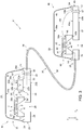
Figure 3 illustrates a multi-device module including the devices ofFigures 1 and 2 functionally coupled together by a flexible printed circuit, according to one embodiment of the present disclosure; -
Figure 4 illustrates a multi-device module including the devices ofFigures 1 and 2 functionally coupled together by a flexible printed circuit and arranged for forming a stacked structure, according to one embodiment of the present disclosure; -
Figure 5 illustrates a multi-device module including transducer devices according to a variant ofFigures 1 and 2 , functionally coupled together by a flexible printed circuit and arranged on opposite sides of a PCB (Printed-Circuit Board) to form a stacked structure according to a further embodiment of the present disclosure; and -
Figure 6 is a schematic illustration of an electronic apparatus including a multi-device module according to any one of the embodiments of the present disclosure. - With reference to
Figure 1 , aMEMS microphone 10 is shown, in a system of spatial co-ordinates x, y, and z. The MEMS microphone 10 comprises a first die (sensor die) 21, which integrates a MEMS structure that provides a first acoustic transducer 1. The first acoustic transducer 1 may be produced according to any technology available and may operate according to any known operating principle. By way of example, the first acoustic transducer 1 is provided with amembrane 2, which is mobile and is made of conductive material, facing a rigid plate 3 (by this term is here meant an element that is relatively rigid with respect to themembrane 2, which is, instead, flexible). Therigid plate 3 includes at least one conductive layer facing themembrane 2, so that themembrane 2 and therigid plate 3 form facing plates of a capacitor. - The
membrane 2, which in use undergoes deformation as a function of incident acoustic pressure waves, is at least partially suspended over astructural layer 5 and directly faces acavity 6, obtained by digging in an area corresponding to arear surface 5b of the structural layer 5 (therear portion 5b is opposite to afront portion 5a of thestructural layer 5 itself, arranged in the proximity of the membrane 2). - The first acoustic transducer 1 is housed in an
internal cavity 8 of apackage 20, together with a second die (control chip) 22 integrating a processing circuit, or ASIC 22'. The ASIC 22', which is in itself known, comprises signal-processing circuits (for example, a charge-amplifier circuit for a capacitive electroacoustic sensor) and/or the components required for enabling proper operation of the microphone, in particular as regards transduction of the acoustic signals. The ASIC 22' is electrically coupled to the first acoustic transducer 1 by an electrical conductor 25' (with the wire-bonding technique), which connects togetherrespective pads second dice - The first and
second dice substrate 23 of thepackage 20. Thefirst die 21 is coupled to thesubstrate 23 on therear surface 5b of thestructural layer 5, for example by an adhesive layer or a layer ofglue 7. Likewise, also thesecond die 22 is coupled to thesubstrate 23 on arear surface 22b thereof, by asolder mask 9 patterned for defining a base for mounting thesecond die 22. According to an embodiment (not shown), thesolder mask 9 may further constitute a supporting base for mounting thefirst die 21. - The integrated ASIC 22' is provided at a
front portion 22a of thesecond die 22, opposite to therear surface 22b. - Appropriate metallization layers and/or conductive through vias (an
electrical path 30 is illustrated, by way of example, inFigure 1 ) are provided in thesubstrate 23 for routing electrical signals towards the outside of thepackage 20. Furtherelectrical connections 25", for example obtained with the wire-bonding technique, are provided for coupling one ormore pads 26c of thesecond die 22 torespective pads 26d of thesubstrate 23. -
Electrical connection elements 29, for example in the form of conductive lands, are provided on anunderside 23b of the substrate 23 (the side facing outwards), for bonding and electrical connection to a PCB. In one embodiment, thesubstrate 23 is a substrate of an LGA (Land-Grid Array) type. In this case, theelectrical connection elements 29 are provided, in particular, in the form of lands. Alternatively, thelands 29 may be replaced by an array of balls or bumps, thus providing a so-called BGA (Ball-Grid Array) package. Theelectrical connection elements 29 are electrically coupled to thepads 26d by respectiveelectrical paths 30 through thesubstrate 23. - The
base substrate 23 includes, according to one embodiment, a multilayer structure made up of one or more layers of conductive material (e.g., metal) separated from one another by layers of rigid dielectric material, for example FR4 (including interwoven glass fibres in an epoxy-resin matrix). Conductive through vias extend through the layers of dielectric material for connecting together one or more metal layers, in a way in itself known. Theelectrical path 30 extends throughout the thickness of thebase substrate 23 for connecting aninner surface 23a thereof, facing theinternal space 8, to theouter space 23b, facing the external environment, for example for enabling direct access to the ASIC 22' for testing or for transfer of signals in use. - Further coupled to the
substrate 23 is a covering element, or cap, 27 of thepackage 20, which encloses the first andsecond dice cap 27 may be made of pre-moulded plastic or metal material. - Also the covering
element 27 may be constituted by a multilayer, for example including one or more plastic and/or metal layers, and may advantageously have a metal coating (not shown) on aninner surface 27a thereof, facing theinternal space 8, in order to provide an electromagnetic shield. Alternatively, the coveringelement 27 is completely made of metal. - The covering
element 27 is further coupled to thebase substrate 23 by coupling regions 24 (solder regions, or regions of glue, or the like) for sealing theinternal space 8 hermetically. - According to one aspect of the present disclosure, throughout the thickness of the
base substrate 23 a through opening, or hole, 28, is made, designed to arranged in acoustic communication thecavity 6 of thefirst die 21 with the environment external to thepackage 20. In what follows, the through opening 28 will also be referred to as "sound port", and thecavity 6 of thefirst die 21 will also be referred to as "acoustic chamber". Further, the term "acoustic communication" is here used with the meaning of "direct acoustic communication", in the sense that generic acoustic waves, or acoustic pressure waves, propagate using as sole propagation medium air (or a possible gas, or mixture of gases, which is equivalent from the standpoint of propagation of sound). - The extension (in the horizontal plane xy) of the
acoustic chamber 6 is greater than the corresponding extension (once again in the horizontal plane xy) of thesound port 28, so that thesound port 28 communicates entirely with theacoustic chamber 6 without it having a direct outlet towards theinternal space 8 of thepackage 20. - According to one aspect of the present disclosure, the
substrate 23 forms part of a printed circuit of a rigid-flex-rigid type 35, and forms a first rigid portion thereof. Printed circuits of a rigid-flex-rigid type are in themselves known in the art and comprise aflexible portion 36, typically a polyamide film, having electrically conductive lines. Theflexible portion 36 is mechanically and electrically coupled, at respective ends thereof, to respective multilayer rigid substrates (one of which, in this case, is thesubstrate 23 ofFigure 1 ). Coupling may be made by soldering one end of theflexible portion 36 to, or integrating it in, thesubstrate 23, during manufacture thereof. The conductive lines of theflexible portion 36 are electrically connected to respective conductive paths of thesubstrate 23, for example to the metal layers integrated in thesubstrate 23, or to pads provided on theface substrate 23. - With reference to the
flexible portion 36, it should be noted that, in this context, by the term "flexible" is meant a structure that may be bent back on itself without undergoing damage or failure, and without jeopardizing its own electrical or electronic functions. The characteristics of flexibility are further a function of the material used and/or of the thickness, the latter ranging, for example, between 50 µm and 150 m. It is evident that it is possible to use aflexible portion 36 with a thickness smaller than the one indicated. Instead, a rigid structure, such as thesubstrate 23, may not be bent back on itself without undergoing damage or failure that would jeopardize the structural stability and/or the electrical or electronic functions thereof. The characteristics of rigidity are further a function of the material used and/or of the thickness, the latter ranging, for example, from 100 µm to 500 µm. - A second rigid portion of the rigid-flex-rigid printed
circuit 35 according to the present disclosure is formed by amultilayer substrate 49 of afurther MEMS microphone 40, illustrated inFigure 2 . Thesubstrate 49 has a structure similar to the one described for thesubstrate 23, i.e., including metal layers that alternate with dielectric layers (e.g., FR4) and are connected together by conductive through vias. In a way similar to what has been described previously, coupling between theflexible portion 36 and thesubstrate 49 may be obtained by soldering one end of theflexible portion 36 to, or by integrating it in, thesubstrate 49, during manufacture thereof. The conductive lines of theflexible portion 36 are electrically connected to respective conductive paths of thesubstrate 49, for example, to the metal layers integrated in thesubstrate 49, or to pads provided on opposite faces of thesubstrate 49. - Thus, as shown in
Figure 3 , theMEMS microphone 10 and theMEMS microphone 40 are mechanically and electrically coupled together by theflexible portion 36, having conductive paths that extend from thesubstrate 23 to thesubstrate 49, arranging them in mechanical and electrical connection and thus forming amulti-device module 61. - As shown in
Figures 2 and3 , theMEMS microphone 40 is similar to theMEMS microphone 10, but does not present the second die (control chip) 22 integrating the processing circuit (ASIC). - The
MEMS microphone 40 thus comprises a die 41, which integrates aMEMS structure 42 provided with amembrane 43, which is mobile and is made of conductive material, facing a rigid plate 44 (by this term is here meant an element that is relatively rigid with respect to themembrane 43, which is instead flexible). Therigid plate 44 includes at least one conductive layer facing themembrane 43 so that themembrane 43 and therigid plate 44 form facing plates of a capacitor. - The
membrane 43, which in use undergoes deformation as a function of incident acoustic pressure waves, is at least partially suspended over astructural layer 45 and directly faces acavity 46, obtained by digging in an area corresponding to arear surface 45b of the structural layer 45 (therear portion 45b is opposite to afront portion 45a of thestructural layer 45 itself, arranged in the proximity of the membrane 43). - The
MEMS structure 42 is housed in aninternal cavity 48 of apackage 50. Thedie 41 is coupled to asubstrate 49 of thepackage 50 on therear surface 45b of thestructural layer 45, for example by an adhesive layer (not shown). - Appropriate metallization layers and/or through vias (
electrical paths 51 are illustrated by way of example inFigure 2 ) are provided in thesubstrate 49 for routing the electrical signals towards the outside of thepackage 50. One or moreelectrical connections 55, obtained with the wire-bonding technique, are provided for coupling one ormore pads 56a of the die 41 torespective pads 56b of thesubstrate 49. -
Electrical connection elements 57 are provided on anunderside 49b of the substrate 49 (the side facing outwards), for bonding and electrical connection to a printed circuit. In one embodiment, thesubstrate 49 is of an LGA type, and theelectrical connection elements 57 are in the form of lands. Alternatively, thelands 57 may be replaced by an array of balls or bumps to provide a BGA package. Theelectrical connection elements 57 are electrically coupled to thepads 56b by respectiveelectrical paths 51 through thesubstrate 49. - Further coupled to the
substrate 49 is a covering element or cap 58 of thepackage 50, which encloses thedie 41. Saidcap 58 may be made of pre-moulded plastic or metal material. - Also the covering
element 58 may be constituted by a multilayer, for example including one or more plastic and/or metal layers, and may advantageously have a metal coating (not shown) on aninner surface 58a thereof, facing theinternal space 48, in order to provide an electromagnetic shield. Alternatively, the coveringelement 58 is completely made of metal. - The covering
element 58 is further coupled to thebase substrate 49 by coupling regions 54 (solder regions, or regions of glue, or the like) for sealing theinternal space 48 hermetically. - Throughout the thickness of the
base substrate 49 a through opening, or hole, 59 is made, designed to arranged in acoustic communication thecavity 46 of the die 41 with the environment external to thepackage 50. In what follows, the throughopening 59 will be referred to as "sound port", and thecavity 46 of the die 21 as "acoustic chamber". Further, the term "acoustic communication" is here used with the meaning of "direct acoustic communication", in the sense that generic acoustic waves, or acoustic pressure waves, propagate using as sole propagation medium air (or a possible gas, or mixture of gases, that is equivalent from the standpoint of acoustic propagation). - The extension (in the horizontal plane xy) of the
acoustic chamber 46 is greater than the corresponding extension (once again in the horizontal plane xy) of thesound port 59, so that thesound port 59 communicates entirely with theacoustic chamber 46 without having a direct outlet towards theinternal space 48 of thepackage 50. - On the basis of what has been described above, it should be noted that the
MEMS microphone 40 does not include an ASIC for processing the signals transduced by theMEMS device 42. In this case, in fact, the signals transduced by theMEMS device 42 are sent to thesecond die 22 of theMEMS microphone 10 throughconductive paths Figure 3 ), which extend in part in (or on) thesubstrate 49, in part in (or on) theflexible portion 36, and in part in (or on) thesubstrate 23. In other words, thedie 41 of theMEMS microphone 40 is electrically coupled to the die 22 of theMEMS microphone 10 via the rigid-flex-rigid printedcircuit 35, for mutual transmission of electrical signals. In this way, it is not necessary to provide a dedicated ASIC in thepackage 50 of theMEMS microphone 40 in so far as the ASIC 22' is shared by both of theMEMS devices 1, 42, with a considerable saving in terms of costs and physical space required. -
Figure 4 illustrates theMEMS microphone 10 and theMEMS microphone 40 coupled together at therespective covering elements - In particular, a coupling layer 62, made, for example, of conductive glue, or non-conductive glue or a biadhesive layer, extends between the covering
element 27 and the coveringelement 58, the latter elements being coupled together by the coupling layer 62. Astack 64 is thus formed, which is constituted by theMEMS microphones circuit 35, as described previously. The presence of theflexible portion 36, which may be completely bent back on itself, renders possible the arrangement in space ofFigure 4 . - This embodiment enables formation of a structure of transducers having the
respective sound ports respective MEMS devices 1, 42 are sent to the ASIC 22', which processes them and, in this example, carries out cancellation of the background noise present in the signal acquired via thesound port 28. -
Figure 5 illustrates amulti-device module 84 including aMEMS microphone 70 and aMEMS microphone 71 coupled together atrespective substrates PCB 79, according to one embodiment of the present disclosure. - The
MEMS microphone 70 is similar to theMEMS microphone 10 ofFigures 1-4 (elements that are in common are designated by the same reference numbers and are not described any further), but differs therefrom in that thesound port 28 obtained through thesubstrate 23 is absent. Instead, theMEMS microphone 70 has a throughhole 74 made through the coveringelement 27 to form a sound port of theMEMS microphone 70. - The
MEMS microphone 71 is similar to theMEMS microphone 40 ofFigures 2-4 (elements that are in common are designated by the same reference numbers and are not described any further), but differs therefrom in that thesound port 59 made through thesubstrate 49 is absent. Instead, theMEMS microphone 71 has a throughhole 78 made through the coveringelement 58 to form a sound port of theMEMS microphone 71. - Providing the
sound ports elements MEMS microphones PCB 79 through therespective substrates MEMS microphone 70, thePCB 79, and theMEMS microphone 71, rendered possible by the presence of theflexible portion 36 of the rigid-flex-rigid printedcircuit 35, which may be completely bent back on itself, which renders possible the arrangement in space ofFigure 4 . ThePCB 79 is designed to be installed, for example, in a portable voice communication device, such as a smartphone. - Unlike what is shown in
Figure 5 , it is also possible to couple theMEMS microphones - It is further evident that the MEMS microphone 10 (having the
sound port 28 obtained through the substrate and including the control chip 22) and the MEMS microphone 71 (having thesound port 78 obtained through the covering element 58) may be coupled together by theflexible portion 36 of the rigid-flex-rigid printedcircuit 35, i.e., by providing theMEMS microphones circuit 35, in a way similar to what has been described previously. - Likewise, the MEMS microphone 40 (having the
sound port 28 obtained through the substrate and without the control chip 22) and the MEMS microphone 70 (having thesound port 78 obtained through the coveringelement 58 and including the control chip 22) may be coupled together by theflexible portion 36 of the rigid-flex-rigid printedcircuit 35, i.e., by providing theMEMS microphones circuit 35, in a way similar to what has been described previously. - According to further variants of the present disclosure, one of the
MEMS microphones Figures 3 and4 may be replaced by a transducer of a different type, for example chosen in the group comprising: a pressure sensor (transducer), a UV sensor, an IR sensor, a generic light-signal sensor (e.g., a photodiode), an accelerometer, or a gyroscope. - In this case, only one between the MEMS microphone 10 (or 40) and the transducer of a different type includes the
control chip 22, in so far as transmission to the ASIC 22' of the signals transduced by the other between the MEMS microphone 10 (or 40) and the transducer of a different type occurs via the rigid-flex-rigid printedcircuit 35. - Likewise, according to further variants of the present disclosure, also one of the
MEMS microphones Figure 5 may be replaced by a transducer of a different type, for example chosen in the group comprising: a pressure sensor (transducer), a UV sensor, an IR sensor, a generic light-signal sensor (e.g., a photodiode), an accelerometer, or a gyroscope. - In this case, only one between the MEMS microphone 70 (or 71) and the transducer of a different type includes the
control chip 22, in so far as transmission to the ASIC 22' of the signals transduced by the other between the MEMS microphone 70 (or 71) and the transducer of a different type occurs via the rigid-flex-rigid printedcircuit 35. -
Figure 6 shows anelectronic device 100 that uses themulti-device module 61 ofFigure 3 , and/or one or both of the stacked configurations shown inFigures 4 and5 . - The
electronic device 100 comprises, in addition to themulti-device module 61, a microprocessor (CPU) 101, amemory block 102, connected to themicroprocessor 101, and an input/output interface 103, for example a keypad and/or a display, which is also connected to themicroprocessor 101. - The
multi-device module 61 communicates with themicroprocessor 101, and in particular transmits the electrical signals processed by the ASIC 22' of the die 22 associated to the MEMS detection structures of thedie 21 and of thedie 41. - The
electronic device 100 is, for example, a mobile communication device, such as a cellphone, a PDA, a notebook, but also a voice recorder, a reader of audio files with voice-recording capacity, a console for video-games, a hydrophone, etc. - The advantages of the invention described previously, according to the various embodiments, emerge clearly from the foregoing description.
- In particular, the present disclosure provides a multi-device module that may be adapted to different configurations according to the need, at the same time reducing the costs and requirements of space in so far as some components (e.g., the ASIC 22') are shared.
- Finally, it is clear that modifications and variations may be made to what has been described and illustrated herein, without thereby departing from the scope of the present invention, as defined in the annexed claims.
- In particular, a different configuration of the MEMS acoustic transducer may be envisaged, specifically as regards the geometrical shape of the constituent elements. In the case where the space inside the package so allows, even a number of MEMS sensors or transducers may possibly be housed within a same package, each configured to detect a respective environmental quantity. Further integrated circuits (e.g., ASICs) may further be provided and housed within the same package, the functions of which are shared between different packages connected together by a flexible printed circuit.
- Further, it is possible to form multi-device modules including any number of packages, connected together by respective flexible PCBs, thus forming a "chain" of devices. In this chain of devices only one of them is provided with a signal-processing integrated circuit (e.g., the ASIC 22'), whereas the remaining devices of the chain communicate with the signal-processing integrated circuit via the conductive lines of the flexible printed circuits and dedicated paths provided within the substrates.
Claims (10)
- A multi-device module (61), comprising:- a first substrate (23), which supports a first MEMS transducer (21, 1) configured to detect a first environmental quantity and to generate a first transduced signal as a function of the first environmental quantity detected, and an integrated circuit (22, 22') operatively coupled to the first MEMS transducer for receiving the first transduced signal; and- a second substrate (49), which supports a second MEMS transducer (41, 42) configured to detect a second environmental quantity and generate a second transduced signal as a function of the second environmental quantity detected,characterized in that it further comprises a flexible printed circuit (36) mechanically coupled to the first and second substrates and electrically coupled to the integrated circuit and to the second MEMS transducer so that said second transduced signal flows, in use, from the second MEMS transducer to the integrated circuit.
- A multi-device module according to claim 1, wherein the first substrate (23), the flexible printed circuit (36), and the second substrate (49) form a printed circuit of a rigid-flex-rigid type (35).
- A multi-device module according to claim 1 or claim 2, wherein:the first and second substrates (23, 49) comprise respective metal and dielectric alternating layers, and respective conductive through vias that extend between one or more respective dielectric layers for electrically connecting together two or more metal layers,and wherein said flexible printed circuit (36) extends within the first and second substrates and is electrically coupled to the integrated circuit (22, 22') and to the second MEMS transducer (41) via one or more of said metal layers and conductive through vias for providing an electrical connection between the second MEMS transducer and the integrated circuit.
- A multi-device module according to claim 3, wherein said dielectric layers are made of a material including interwoven glass fibres in an epoxy-resin matrix, or FR4.
- A multi-device module according to any one of the preceding claims, wherein said integrated circuit (22, 22') is an ASIC.
- A multi-device module according to any one of the preceding claims, wherein the first MEMS transducer and the second MEMS transducer are chosen in the group comprising: a pressure sensor (transducer), a light-flow sensor, a UV sensor, an IR sensor, an accelerometer, and a gyroscope.
- A multi-device module according to any one of the preceding claims, further comprising:- a first covering element (27) coupled to the first substrate (23) and defining, together with the first substrate, a first package (20) that houses the first MEMS transducer and the integrated circuit; and- a second covering element (58) coupled to the second substrate (49) and defining, together with the second substrate, a second package (50) that houses the second MEMS transducer,wherein the first and second MEMS transducers are acoustic transducers, the first substrate having a first acoustic-access opening (28) in acoustic communication with an environment external to the first package (20), and the second substrate having a respective second acoustic-access opening (59) in acoustic communication with an environment external to the second package (50),
said first and second packages being mechanically coupled together at the respective covering elements. - A multi-device module according to any one of claims 1-6, further comprising:- a first covering element (27), which extends over the first substrate (23) and defines with the first substrate a first package (20) that houses the first MEMS transducer and the integrated circuit; and- a second covering element (58), which extends over the second substrate (49) and defines with the second substrate a second package (50) that houses the second MEMS transducer;wherein the first and second MEMS transducers are acoustic transducers, the first covering element (27) having a first acoustic-access opening (74) in acoustic communication with an environment external to the first package (20), and the second covering element (58) having a respective second acoustic-access opening (78) in acoustic communication with an environment external to the second package (50),
said first and second packages being mechanically and electrically coupled to respective faces of an integrated-circuit board via the respective first and second substrates for forming a stacked structure. - An electronic apparatus (100), comprising:a microprocessor; anda multi-device module according to any one of claims 1-8, coupled to the microprocessor, said electronic apparatus being at least one among: a cellphone, a PDA, a notebook, a voice recorder, an audio reader with functions of voice recorder, a console for video-games, a hydrophone.
- A method for manufacturing a multi-device module (61), comprising the steps of:- forming a first package which includes a first MEMS transducer (21, 1) and an integrated circuit, the first MEMS transducer being configured to detect a first environmental quantity and to generate a first transduced signal as a function of the first environmental quantity detected, the integrated circuit (22, 22') being operatively coupled to the first MEMS transducer for receiving the first transduced signal; and- forming a second package which includes a second MEMS transducer (41, 42) configured to detect a second environmental quantity and to generate a second transduced signal as a function of the second environmental quantity detected,characterized in that it further comprises the steps of:- mechanically and electrically couple a flexible printed circuit (36) to the first and second package, in which the second MEMS transducer is coupled to the integrated circuit through the flexible printed circuit (36), the integrated circuit being configured to receive the second transduced signal from the second MEMS transducer (41, 42).
Applications Claiming Priority (1)
| Application Number | Priority Date | Filing Date | Title |
|---|---|---|---|
| ITUA2016A002957A ITUA20162957A1 (en) | 2016-04-28 | 2016-04-28 | MULTI-DEVICE TRANSDUCTION MODULE, EQUIPMENT INCLUDING TRANSDUCTION MODULE AND METHOD OF MANUFACTURE OF TRANSDUCTION MODULE |
Publications (2)
| Publication Number | Publication Date |
|---|---|
| EP3240306A1 true EP3240306A1 (en) | 2017-11-01 |
| EP3240306B1 EP3240306B1 (en) | 2021-09-22 |
Family
ID=56555624
Family Applications (1)
| Application Number | Title | Priority Date | Filing Date |
|---|---|---|---|
| EP17162651.8A Active EP3240306B1 (en) | 2016-04-28 | 2017-03-23 | Multi-device transducer module, apparatus including the transducer module and method of manufacturing the transducer module |
Country Status (4)
| Country | Link |
|---|---|
| US (2) | US10091587B2 (en) |
| EP (1) | EP3240306B1 (en) |
| CN (2) | CN107343249B (en) |
| IT (1) | ITUA20162957A1 (en) |
Families Citing this family (19)
| Publication number | Priority date | Publication date | Assignee | Title |
|---|---|---|---|---|
| ITUA20162957A1 (en) * | 2016-04-28 | 2017-10-28 | St Microelectronics Srl | MULTI-DEVICE TRANSDUCTION MODULE, EQUIPMENT INCLUDING TRANSDUCTION MODULE AND METHOD OF MANUFACTURE OF TRANSDUCTION MODULE |
| IT201600121210A1 (en) * | 2016-11-30 | 2018-05-30 | St Microelectronics Srl | MULTI-DEVICE TRANSDUCTION MODULE, ELECTRONIC EQUIPMENT INCLUDING THE TRANSDUCTION FORM AND METHOD OF MANUFACTURING THE TRANSDUCTION MODULE |
| WO2019246079A1 (en) * | 2018-06-19 | 2019-12-26 | W.L. Gore & Associates, Inc. | Protection of integrated low power system designed to monitor the acoustic environment |
| WO2020016780A1 (en) | 2018-07-19 | 2020-01-23 | Cochlear Limited | Sub-surface indicator lighting |
| CN110650418A (en) * | 2019-10-24 | 2020-01-03 | 朝阳聚声泰(信丰)科技有限公司 | Photosensitive intelligent MEMS microphone |
| US11897763B2 (en) | 2019-12-16 | 2024-02-13 | Stmicroelectronics, Inc. | Capless semiconductor package with a micro-electromechanical system (MEMS) |
| US11228846B2 (en) * | 2020-02-14 | 2022-01-18 | Apple Inc. | Sensor assembly for electronic device |
| US12172887B2 (en) * | 2020-07-12 | 2024-12-24 | xMEMS Labs, Inc. | Sound producing package structure including sound producing membranes actuated toward cavity center |
| US11912564B2 (en) * | 2020-07-31 | 2024-02-27 | Knowles Electronics, Llc | Sensor package including a substrate with an inductor layer |
| CN112225169A (en) * | 2020-11-02 | 2021-01-15 | 华景传感科技(无锡)有限公司 | A pressure module and method of making the same |
| TWI756976B (en) * | 2020-12-10 | 2022-03-01 | 美律實業股份有限公司 | Microphone module |
| CN115304021B (en) * | 2021-05-07 | 2024-12-27 | 玻音先创科技股份有限公司 | MEMS Acoustic Wave Transducer |
| US11758312B2 (en) * | 2021-06-01 | 2023-09-12 | Xmems Taiwan Co., Ltd. | Sound producing package structure and manufacturing method thereof |
| US11760627B2 (en) | 2021-06-10 | 2023-09-19 | Invensense, Inc. | MEMS stress reduction structure embedded into package |
| CN113301486B (en) * | 2021-06-17 | 2022-04-29 | 甬矽电子(宁波)股份有限公司 | Double-silicon-microphone packaging structure and preparation method thereof |
| CN215453270U (en) * | 2021-07-07 | 2022-01-07 | 瑞声声学科技(深圳)有限公司 | microphone |
| US11787551B1 (en) | 2022-10-06 | 2023-10-17 | Archer Aviation, Inc. | Vertical takeoff and landing aircraft electric engine configuration |
| US12227300B2 (en) | 2022-10-06 | 2025-02-18 | Archer Aviation Inc. | Systems and methods for oil maintenance in gearboxes for eVTOL aircraft |
| WO2024077248A1 (en) | 2022-10-06 | 2024-04-11 | Archer Aviation Inc. | Systems, methods, and mechanical designs for inverters for evtol aircraft |
Citations (2)
| Publication number | Priority date | Publication date | Assignee | Title |
|---|---|---|---|---|
| EP2552127A1 (en) * | 2010-06-01 | 2013-01-30 | Funai Electric Co., Ltd. | Microphone unit and audio input device provided with same |
| US20150023523A1 (en) | 2013-07-22 | 2015-01-22 | Infineon Technologies Ag | Surface Mountable Microphone Package, a Microphone Arrangement, a Mobile Phone and a Method for Recording Microphone Signals |
Family Cites Families (21)
| Publication number | Priority date | Publication date | Assignee | Title |
|---|---|---|---|---|
| US5742484A (en) * | 1997-02-18 | 1998-04-21 | Motorola, Inc. | Flexible connector for circuit boards |
| US7429495B2 (en) * | 2002-08-07 | 2008-09-30 | Chang-Feng Wan | System and method of fabricating micro cavities |
| US20070215962A1 (en) * | 2006-03-20 | 2007-09-20 | Knowles Elecronics, Llc | Microelectromechanical system assembly and method for manufacturing thereof |
| CN201226592Y (en) * | 2008-06-23 | 2009-04-22 | 东莞泉声电子有限公司 | Silicon microphone packaged by flexible circuit board |
| US8193596B2 (en) * | 2008-09-03 | 2012-06-05 | Solid State System Co., Ltd. | Micro-electro-mechanical systems (MEMS) package |
| US8472648B2 (en) * | 2009-01-20 | 2013-06-25 | General Mems Corporation | Miniature MEMS condenser microphone package and fabrication method thereof |
| US8199939B2 (en) * | 2009-01-21 | 2012-06-12 | Nokia Corporation | Microphone package |
| EP2252077B1 (en) * | 2009-05-11 | 2012-07-11 | STMicroelectronics Srl | Assembly of a capacitive acoustic transducer of the microelectromechanical type and package thereof |
| CN102428711A (en) * | 2009-05-18 | 2012-04-25 | 美商楼氏电子有限公司 | Microphone with reduced vibration sensitivity |
| WO2011087770A2 (en) * | 2009-12-22 | 2011-07-21 | Mh Acoustics, Llc | Surface-mounted microphone arrays on flexible printed circuit boards |
| US8577063B2 (en) * | 2010-02-18 | 2013-11-05 | Analog Devices, Inc. | Packages and methods for packaging MEMS microphone devices |
| JP4947191B2 (en) * | 2010-06-01 | 2012-06-06 | オムロン株式会社 | microphone |
| US9156673B2 (en) * | 2010-09-18 | 2015-10-13 | Fairchild Semiconductor Corporation | Packaging to reduce stress on microelectromechanical systems |
| US9276080B2 (en) * | 2012-03-09 | 2016-03-01 | Mcube, Inc. | Methods and structures of integrated MEMS-CMOS devices |
| US8447057B2 (en) * | 2011-03-18 | 2013-05-21 | Analog Devices, Inc. | Packages and methods for packaging MEMS microphone devices |
| US8804982B2 (en) | 2011-04-02 | 2014-08-12 | Harman International Industries, Inc. | Dual cell MEMS assembly |
| JP6271887B2 (en) * | 2013-07-10 | 2018-01-31 | キヤノン株式会社 | Capacitive transducer, probe, and subject information acquisition apparatus |
| US20160100256A1 (en) * | 2013-10-30 | 2016-04-07 | Knowles Electronics, Llc | Acoustic Assembly and Method of Manufacturing The Same |
| DE102014100464B4 (en) | 2014-01-16 | 2022-02-17 | Tdk Corporation | Multi MEMS module |
| US9497529B2 (en) * | 2014-02-18 | 2016-11-15 | Apple Inc. | Microphone port with foreign material ingress protection |
| ITUA20162957A1 (en) * | 2016-04-28 | 2017-10-28 | St Microelectronics Srl | MULTI-DEVICE TRANSDUCTION MODULE, EQUIPMENT INCLUDING TRANSDUCTION MODULE AND METHOD OF MANUFACTURE OF TRANSDUCTION MODULE |
-
2016
- 2016-04-28 IT ITUA2016A002957A patent/ITUA20162957A1/en unknown
- 2016-12-13 US US15/377,627 patent/US10091587B2/en active Active
- 2016-12-20 CN CN201611182133.0A patent/CN107343249B/en active Active
- 2016-12-20 CN CN201621402817.2U patent/CN206380092U/en active Active
-
2017
- 2017-03-23 EP EP17162651.8A patent/EP3240306B1/en active Active
-
2018
- 2018-09-20 US US16/137,439 patent/US10531204B2/en active Active
Patent Citations (2)
| Publication number | Priority date | Publication date | Assignee | Title |
|---|---|---|---|---|
| EP2552127A1 (en) * | 2010-06-01 | 2013-01-30 | Funai Electric Co., Ltd. | Microphone unit and audio input device provided with same |
| US20150023523A1 (en) | 2013-07-22 | 2015-01-22 | Infineon Technologies Ag | Surface Mountable Microphone Package, a Microphone Arrangement, a Mobile Phone and a Method for Recording Microphone Signals |
Also Published As
| Publication number | Publication date |
|---|---|
| CN107343249B (en) | 2019-12-31 |
| US10531204B2 (en) | 2020-01-07 |
| US20170318396A1 (en) | 2017-11-02 |
| ITUA20162957A1 (en) | 2017-10-28 |
| EP3240306B1 (en) | 2021-09-22 |
| US20190028815A1 (en) | 2019-01-24 |
| US10091587B2 (en) | 2018-10-02 |
| CN107343249A (en) | 2017-11-10 |
| CN206380092U (en) | 2017-08-04 |
Similar Documents
| Publication | Publication Date | Title |
|---|---|---|
| EP3240306B1 (en) | Multi-device transducer module, apparatus including the transducer module and method of manufacturing the transducer module | |
| US10597287B2 (en) | Multi-chamber transducer module, apparatus including the multi-chamber transducer module and method of manufacturing the multi-chamber transducer module | |
| US8837754B2 (en) | Microelectromechanical transducer and corresponding assembly process | |
| CN104140071B (en) | The chip level assembly of MEMS sensor device and related MEMS sensor device | |
| US9998812B2 (en) | Surface mountable microphone package, a microphone arrangement, a mobile phone and a method for recording microphone signals | |
| CN102088653B (en) | microphone | |
| EP3330688B1 (en) | Multi-transducer modulus, electronic apparatus including the multi-transducer modulus and method for manufacturing the multi-transducer modulus | |
| US20150117681A1 (en) | Acoustic Assembly and Method of Manufacturing The Same | |
| PL209935B1 (en) | Silicon−based sensor system | |
| US10252906B2 (en) | Package for MEMS device and process | |
| KR101870023B1 (en) | System and method for a packaged mems device | |
| CN109644307B (en) | Microphone and pressure sensor package and method of making microphone and pressure sensor package | |
| CN116405857B (en) | A noise reduction MEMS microphone and electronic equipment | |
| WO2016102924A1 (en) | Mems transducer package | |
| CN107113485B (en) | Leadframe-based chip carriers used in the fabrication of MEMS transducer packages | |
| CN214591968U (en) | MEMS microphone structure | |
| CN112738699A (en) | MEMS microphone structure |
Legal Events
| Date | Code | Title | Description |
|---|---|---|---|
| PUAI | Public reference made under article 153(3) epc to a published international application that has entered the european phase |
Free format text: ORIGINAL CODE: 0009012 |
|
| STAA | Information on the status of an ep patent application or granted ep patent |
Free format text: STATUS: THE APPLICATION HAS BEEN PUBLISHED |
|
| AK | Designated contracting states |
Kind code of ref document: A1 Designated state(s): AL AT BE BG CH CY CZ DE DK EE ES FI FR GB GR HR HU IE IS IT LI LT LU LV MC MK MT NL NO PL PT RO RS SE SI SK SM TR |
|
| AX | Request for extension of the european patent |
Extension state: BA ME |
|
| STAA | Information on the status of an ep patent application or granted ep patent |
Free format text: STATUS: REQUEST FOR EXAMINATION WAS MADE |
|
| 17P | Request for examination filed |
Effective date: 20180430 |
|
| RBV | Designated contracting states (corrected) |
Designated state(s): AL AT BE BG CH CY CZ DE DK EE ES FI FR GB GR HR HU IE IS IT LI LT LU LV MC MK MT NL NO PL PT RO RS SE SI SK SM TR |
|
| STAA | Information on the status of an ep patent application or granted ep patent |
Free format text: STATUS: EXAMINATION IS IN PROGRESS |
|
| 17Q | First examination report despatched |
Effective date: 20201030 |
|
| GRAP | Despatch of communication of intention to grant a patent |
Free format text: ORIGINAL CODE: EPIDOSNIGR1 |
|
| STAA | Information on the status of an ep patent application or granted ep patent |
Free format text: STATUS: GRANT OF PATENT IS INTENDED |
|
| RIC1 | Information provided on ipc code assigned before grant |
Ipc: H04R 3/00 20060101ALN20210317BHEP Ipc: H04M 1/03 20060101ALN20210317BHEP Ipc: B81C 1/00 20060101ALI20210317BHEP Ipc: B06B 1/02 20060101ALI20210317BHEP Ipc: H04R 19/00 20060101AFI20210317BHEP |
|
| GRAJ | Information related to disapproval of communication of intention to grant by the applicant or resumption of examination proceedings by the epo deleted |
Free format text: ORIGINAL CODE: EPIDOSDIGR1 |
|
| STAA | Information on the status of an ep patent application or granted ep patent |
Free format text: STATUS: EXAMINATION IS IN PROGRESS |
|
| INTG | Intention to grant announced |
Effective date: 20210401 |
|
| GRAP | Despatch of communication of intention to grant a patent |
Free format text: ORIGINAL CODE: EPIDOSNIGR1 |
|
| STAA | Information on the status of an ep patent application or granted ep patent |
Free format text: STATUS: GRANT OF PATENT IS INTENDED |
|
| INTC | Intention to grant announced (deleted) | ||
| RIC1 | Information provided on ipc code assigned before grant |
Ipc: H04R 3/00 20060101ALN20210427BHEP Ipc: H04M 1/03 20060101ALN20210427BHEP Ipc: B81C 1/00 20060101ALI20210427BHEP Ipc: B06B 1/02 20060101ALI20210427BHEP Ipc: H04R 19/00 20060101AFI20210427BHEP |
|
| INTG | Intention to grant announced |
Effective date: 20210517 |
|
| GRAS | Grant fee paid |
Free format text: ORIGINAL CODE: EPIDOSNIGR3 |
|
| GRAA | (expected) grant |
Free format text: ORIGINAL CODE: 0009210 |
|
| STAA | Information on the status of an ep patent application or granted ep patent |
Free format text: STATUS: THE PATENT HAS BEEN GRANTED |
|
| AK | Designated contracting states |
Kind code of ref document: B1 Designated state(s): AL AT BE BG CH CY CZ DE DK EE ES FI FR GB GR HR HU IE IS IT LI LT LU LV MC MK MT NL NO PL PT RO RS SE SI SK SM TR |
|
| REG | Reference to a national code |
Ref country code: GB Ref legal event code: FG4D |
|
| REG | Reference to a national code |
Ref country code: IE Ref legal event code: FG4D |
|
| REG | Reference to a national code |
Ref country code: DE Ref legal event code: R096 Ref document number: 602017046283 Country of ref document: DE |
|
| REG | Reference to a national code |
Ref country code: CH Ref legal event code: EP Ref country code: AT Ref legal event code: REF Ref document number: 1433283 Country of ref document: AT Kind code of ref document: T Effective date: 20211015 |
|
| REG | Reference to a national code |
Ref country code: LT Ref legal event code: MG9D |
|
| REG | Reference to a national code |
Ref country code: NL Ref legal event code: MP Effective date: 20210922 |
|
| PG25 | Lapsed in a contracting state [announced via postgrant information from national office to epo] |
Ref country code: SE Free format text: LAPSE BECAUSE OF FAILURE TO SUBMIT A TRANSLATION OF THE DESCRIPTION OR TO PAY THE FEE WITHIN THE PRESCRIBED TIME-LIMIT Effective date: 20210922 Ref country code: RS Free format text: LAPSE BECAUSE OF FAILURE TO SUBMIT A TRANSLATION OF THE DESCRIPTION OR TO PAY THE FEE WITHIN THE PRESCRIBED TIME-LIMIT Effective date: 20210922 Ref country code: NO Free format text: LAPSE BECAUSE OF FAILURE TO SUBMIT A TRANSLATION OF THE DESCRIPTION OR TO PAY THE FEE WITHIN THE PRESCRIBED TIME-LIMIT Effective date: 20211222 Ref country code: HR Free format text: LAPSE BECAUSE OF FAILURE TO SUBMIT A TRANSLATION OF THE DESCRIPTION OR TO PAY THE FEE WITHIN THE PRESCRIBED TIME-LIMIT Effective date: 20210922 Ref country code: FI Free format text: LAPSE BECAUSE OF FAILURE TO SUBMIT A TRANSLATION OF THE DESCRIPTION OR TO PAY THE FEE WITHIN THE PRESCRIBED TIME-LIMIT Effective date: 20210922 Ref country code: LT Free format text: LAPSE BECAUSE OF FAILURE TO SUBMIT A TRANSLATION OF THE DESCRIPTION OR TO PAY THE FEE WITHIN THE PRESCRIBED TIME-LIMIT Effective date: 20210922 Ref country code: BG Free format text: LAPSE BECAUSE OF FAILURE TO SUBMIT A TRANSLATION OF THE DESCRIPTION OR TO PAY THE FEE WITHIN THE PRESCRIBED TIME-LIMIT Effective date: 20211222 |
|
| REG | Reference to a national code |
Ref country code: AT Ref legal event code: MK05 Ref document number: 1433283 Country of ref document: AT Kind code of ref document: T Effective date: 20210922 |
|
| PG25 | Lapsed in a contracting state [announced via postgrant information from national office to epo] |
Ref country code: LV Free format text: LAPSE BECAUSE OF FAILURE TO SUBMIT A TRANSLATION OF THE DESCRIPTION OR TO PAY THE FEE WITHIN THE PRESCRIBED TIME-LIMIT Effective date: 20210922 Ref country code: GR Free format text: LAPSE BECAUSE OF FAILURE TO SUBMIT A TRANSLATION OF THE DESCRIPTION OR TO PAY THE FEE WITHIN THE PRESCRIBED TIME-LIMIT Effective date: 20211223 |
|
| PG25 | Lapsed in a contracting state [announced via postgrant information from national office to epo] |
Ref country code: AT Free format text: LAPSE BECAUSE OF FAILURE TO SUBMIT A TRANSLATION OF THE DESCRIPTION OR TO PAY THE FEE WITHIN THE PRESCRIBED TIME-LIMIT Effective date: 20210922 |
|
| PG25 | Lapsed in a contracting state [announced via postgrant information from national office to epo] |
Ref country code: IS Free format text: LAPSE BECAUSE OF FAILURE TO SUBMIT A TRANSLATION OF THE DESCRIPTION OR TO PAY THE FEE WITHIN THE PRESCRIBED TIME-LIMIT Effective date: 20220122 Ref country code: SK Free format text: LAPSE BECAUSE OF FAILURE TO SUBMIT A TRANSLATION OF THE DESCRIPTION OR TO PAY THE FEE WITHIN THE PRESCRIBED TIME-LIMIT Effective date: 20210922 Ref country code: RO Free format text: LAPSE BECAUSE OF FAILURE TO SUBMIT A TRANSLATION OF THE DESCRIPTION OR TO PAY THE FEE WITHIN THE PRESCRIBED TIME-LIMIT Effective date: 20210922 Ref country code: PT Free format text: LAPSE BECAUSE OF FAILURE TO SUBMIT A TRANSLATION OF THE DESCRIPTION OR TO PAY THE FEE WITHIN THE PRESCRIBED TIME-LIMIT Effective date: 20220124 Ref country code: PL Free format text: LAPSE BECAUSE OF FAILURE TO SUBMIT A TRANSLATION OF THE DESCRIPTION OR TO PAY THE FEE WITHIN THE PRESCRIBED TIME-LIMIT Effective date: 20210922 Ref country code: NL Free format text: LAPSE BECAUSE OF FAILURE TO SUBMIT A TRANSLATION OF THE DESCRIPTION OR TO PAY THE FEE WITHIN THE PRESCRIBED TIME-LIMIT Effective date: 20210922 Ref country code: ES Free format text: LAPSE BECAUSE OF FAILURE TO SUBMIT A TRANSLATION OF THE DESCRIPTION OR TO PAY THE FEE WITHIN THE PRESCRIBED TIME-LIMIT Effective date: 20210922 Ref country code: EE Free format text: LAPSE BECAUSE OF FAILURE TO SUBMIT A TRANSLATION OF THE DESCRIPTION OR TO PAY THE FEE WITHIN THE PRESCRIBED TIME-LIMIT Effective date: 20210922 Ref country code: CZ Free format text: LAPSE BECAUSE OF FAILURE TO SUBMIT A TRANSLATION OF THE DESCRIPTION OR TO PAY THE FEE WITHIN THE PRESCRIBED TIME-LIMIT Effective date: 20210922 Ref country code: AL Free format text: LAPSE BECAUSE OF FAILURE TO SUBMIT A TRANSLATION OF THE DESCRIPTION OR TO PAY THE FEE WITHIN THE PRESCRIBED TIME-LIMIT Effective date: 20210922 |
|
| REG | Reference to a national code |
Ref country code: DE Ref legal event code: R097 Ref document number: 602017046283 Country of ref document: DE |
|
| PG25 | Lapsed in a contracting state [announced via postgrant information from national office to epo] |
Ref country code: DK Free format text: LAPSE BECAUSE OF FAILURE TO SUBMIT A TRANSLATION OF THE DESCRIPTION OR TO PAY THE FEE WITHIN THE PRESCRIBED TIME-LIMIT Effective date: 20210922 |
|
| PLBE | No opposition filed within time limit |
Free format text: ORIGINAL CODE: 0009261 |
|
| STAA | Information on the status of an ep patent application or granted ep patent |
Free format text: STATUS: NO OPPOSITION FILED WITHIN TIME LIMIT |
|
| 26N | No opposition filed |
Effective date: 20220623 |
|
| PG25 | Lapsed in a contracting state [announced via postgrant information from national office to epo] |
Ref country code: MC Free format text: LAPSE BECAUSE OF FAILURE TO SUBMIT A TRANSLATION OF THE DESCRIPTION OR TO PAY THE FEE WITHIN THE PRESCRIBED TIME-LIMIT Effective date: 20210922 |
|
| REG | Reference to a national code |
Ref country code: CH Ref legal event code: PL |
|
| GBPC | Gb: european patent ceased through non-payment of renewal fee |
Effective date: 20220323 |
|
| PG25 | Lapsed in a contracting state [announced via postgrant information from national office to epo] |
Ref country code: SI Free format text: LAPSE BECAUSE OF FAILURE TO SUBMIT A TRANSLATION OF THE DESCRIPTION OR TO PAY THE FEE WITHIN THE PRESCRIBED TIME-LIMIT Effective date: 20210922 |
|
| REG | Reference to a national code |
Ref country code: BE Ref legal event code: MM Effective date: 20220331 |
|
| PG25 | Lapsed in a contracting state [announced via postgrant information from national office to epo] |
Ref country code: LU Free format text: LAPSE BECAUSE OF NON-PAYMENT OF DUE FEES Effective date: 20220323 Ref country code: LI Free format text: LAPSE BECAUSE OF NON-PAYMENT OF DUE FEES Effective date: 20220331 Ref country code: IT Free format text: LAPSE BECAUSE OF FAILURE TO SUBMIT A TRANSLATION OF THE DESCRIPTION OR TO PAY THE FEE WITHIN THE PRESCRIBED TIME-LIMIT Effective date: 20210922 Ref country code: IE Free format text: LAPSE BECAUSE OF NON-PAYMENT OF DUE FEES Effective date: 20220323 Ref country code: GB Free format text: LAPSE BECAUSE OF NON-PAYMENT OF DUE FEES Effective date: 20220323 Ref country code: FR Free format text: LAPSE BECAUSE OF NON-PAYMENT OF DUE FEES Effective date: 20220331 Ref country code: CH Free format text: LAPSE BECAUSE OF NON-PAYMENT OF DUE FEES Effective date: 20220331 |
|
| PG25 | Lapsed in a contracting state [announced via postgrant information from national office to epo] |
Ref country code: BE Free format text: LAPSE BECAUSE OF NON-PAYMENT OF DUE FEES Effective date: 20220331 |
|
| PG25 | Lapsed in a contracting state [announced via postgrant information from national office to epo] |
Ref country code: HU Free format text: LAPSE BECAUSE OF FAILURE TO SUBMIT A TRANSLATION OF THE DESCRIPTION OR TO PAY THE FEE WITHIN THE PRESCRIBED TIME-LIMIT; INVALID AB INITIO Effective date: 20170323 |
|
| PG25 | Lapsed in a contracting state [announced via postgrant information from national office to epo] |
Ref country code: SM Free format text: LAPSE BECAUSE OF FAILURE TO SUBMIT A TRANSLATION OF THE DESCRIPTION OR TO PAY THE FEE WITHIN THE PRESCRIBED TIME-LIMIT Effective date: 20210922 Ref country code: MK Free format text: LAPSE BECAUSE OF FAILURE TO SUBMIT A TRANSLATION OF THE DESCRIPTION OR TO PAY THE FEE WITHIN THE PRESCRIBED TIME-LIMIT Effective date: 20210922 Ref country code: CY Free format text: LAPSE BECAUSE OF FAILURE TO SUBMIT A TRANSLATION OF THE DESCRIPTION OR TO PAY THE FEE WITHIN THE PRESCRIBED TIME-LIMIT Effective date: 20210922 |
|
| PG25 | Lapsed in a contracting state [announced via postgrant information from national office to epo] |
Ref country code: MT Free format text: LAPSE BECAUSE OF FAILURE TO SUBMIT A TRANSLATION OF THE DESCRIPTION OR TO PAY THE FEE WITHIN THE PRESCRIBED TIME-LIMIT Effective date: 20210922 |
|
| PGFP | Annual fee paid to national office [announced via postgrant information from national office to epo] |
Ref country code: DE Payment date: 20250218 Year of fee payment: 9 |
|
| PG25 | Lapsed in a contracting state [announced via postgrant information from national office to epo] |
Ref country code: TR Free format text: LAPSE BECAUSE OF FAILURE TO SUBMIT A TRANSLATION OF THE DESCRIPTION OR TO PAY THE FEE WITHIN THE PRESCRIBED TIME-LIMIT Effective date: 20210922 |