EP3240170A1 - Non-isolated power supply device - Google Patents
Non-isolated power supply device Download PDFInfo
- Publication number
- EP3240170A1 EP3240170A1 EP15872914.5A EP15872914A EP3240170A1 EP 3240170 A1 EP3240170 A1 EP 3240170A1 EP 15872914 A EP15872914 A EP 15872914A EP 3240170 A1 EP3240170 A1 EP 3240170A1
- Authority
- EP
- European Patent Office
- Prior art keywords
- voltage
- inductor
- power supply
- external terminal
- current
- Prior art date
- Legal status (The legal status is an assumption and is not a legal conclusion. Google has not performed a legal analysis and makes no representation as to the accuracy of the status listed.)
- Withdrawn
Links
- 238000009499 grossing Methods 0.000 claims abstract description 18
- 238000006243 chemical reaction Methods 0.000 claims abstract description 11
- 230000004044 response Effects 0.000 claims abstract description 4
- 239000003990 capacitor Substances 0.000 claims description 8
- 239000004065 semiconductor Substances 0.000 abstract description 3
- 230000002708 enhancing effect Effects 0.000 abstract 1
- 238000001514 detection method Methods 0.000 description 27
- 238000000034 method Methods 0.000 description 8
- 230000008859 change Effects 0.000 description 4
- 230000008878 coupling Effects 0.000 description 2
- 238000010168 coupling process Methods 0.000 description 2
- 238000005859 coupling reaction Methods 0.000 description 2
- 230000015556 catabolic process Effects 0.000 description 1
- 230000007423 decrease Effects 0.000 description 1
- 238000006731 degradation reaction Methods 0.000 description 1
- 230000003111 delayed effect Effects 0.000 description 1
- 238000010586 diagram Methods 0.000 description 1
- 230000000694 effects Effects 0.000 description 1
- 230000008569 process Effects 0.000 description 1
- 230000001360 synchronised effect Effects 0.000 description 1
Images



Classifications
-
- H—ELECTRICITY
- H05—ELECTRIC TECHNIQUES NOT OTHERWISE PROVIDED FOR
- H05B—ELECTRIC HEATING; ELECTRIC LIGHT SOURCES NOT OTHERWISE PROVIDED FOR; CIRCUIT ARRANGEMENTS FOR ELECTRIC LIGHT SOURCES, IN GENERAL
- H05B45/00—Circuit arrangements for operating light-emitting diodes [LED]
- H05B45/30—Driver circuits
- H05B45/37—Converter circuits
- H05B45/3725—Switched mode power supply [SMPS]
- H05B45/38—Switched mode power supply [SMPS] using boost topology
-
- H—ELECTRICITY
- H02—GENERATION; CONVERSION OR DISTRIBUTION OF ELECTRIC POWER
- H02M—APPARATUS FOR CONVERSION BETWEEN AC AND AC, BETWEEN AC AND DC, OR BETWEEN DC AND DC, AND FOR USE WITH MAINS OR SIMILAR POWER SUPPLY SYSTEMS; CONVERSION OF DC OR AC INPUT POWER INTO SURGE OUTPUT POWER; CONTROL OR REGULATION THEREOF
- H02M1/00—Details of apparatus for conversion
- H02M1/08—Circuits specially adapted for the generation of control voltages for semiconductor devices incorporated in static converters
-
- H—ELECTRICITY
- H02—GENERATION; CONVERSION OR DISTRIBUTION OF ELECTRIC POWER
- H02M—APPARATUS FOR CONVERSION BETWEEN AC AND AC, BETWEEN AC AND DC, OR BETWEEN DC AND DC, AND FOR USE WITH MAINS OR SIMILAR POWER SUPPLY SYSTEMS; CONVERSION OF DC OR AC INPUT POWER INTO SURGE OUTPUT POWER; CONTROL OR REGULATION THEREOF
- H02M1/00—Details of apparatus for conversion
- H02M1/08—Circuits specially adapted for the generation of control voltages for semiconductor devices incorporated in static converters
- H02M1/083—Circuits specially adapted for the generation of control voltages for semiconductor devices incorporated in static converters for the ignition at the zero crossing of the voltage or the current
-
- H—ELECTRICITY
- H02—GENERATION; CONVERSION OR DISTRIBUTION OF ELECTRIC POWER
- H02M—APPARATUS FOR CONVERSION BETWEEN AC AND AC, BETWEEN AC AND DC, OR BETWEEN DC AND DC, AND FOR USE WITH MAINS OR SIMILAR POWER SUPPLY SYSTEMS; CONVERSION OF DC OR AC INPUT POWER INTO SURGE OUTPUT POWER; CONTROL OR REGULATION THEREOF
- H02M1/00—Details of apparatus for conversion
- H02M1/14—Arrangements for reducing ripples from DC input or output
-
- H—ELECTRICITY
- H02—GENERATION; CONVERSION OR DISTRIBUTION OF ELECTRIC POWER
- H02M—APPARATUS FOR CONVERSION BETWEEN AC AND AC, BETWEEN AC AND DC, OR BETWEEN DC AND DC, AND FOR USE WITH MAINS OR SIMILAR POWER SUPPLY SYSTEMS; CONVERSION OF DC OR AC INPUT POWER INTO SURGE OUTPUT POWER; CONTROL OR REGULATION THEREOF
- H02M3/00—Conversion of DC power input into DC power output
- H02M3/02—Conversion of DC power input into DC power output without intermediate conversion into AC
- H02M3/04—Conversion of DC power input into DC power output without intermediate conversion into AC by static converters
- H02M3/10—Conversion of DC power input into DC power output without intermediate conversion into AC by static converters using discharge tubes with control electrode or semiconductor devices with control electrode
- H02M3/145—Conversion of DC power input into DC power output without intermediate conversion into AC by static converters using discharge tubes with control electrode or semiconductor devices with control electrode using devices of a triode or transistor type requiring continuous application of a control signal
- H02M3/155—Conversion of DC power input into DC power output without intermediate conversion into AC by static converters using discharge tubes with control electrode or semiconductor devices with control electrode using devices of a triode or transistor type requiring continuous application of a control signal using semiconductor devices only
-
- H—ELECTRICITY
- H02—GENERATION; CONVERSION OR DISTRIBUTION OF ELECTRIC POWER
- H02M—APPARATUS FOR CONVERSION BETWEEN AC AND AC, BETWEEN AC AND DC, OR BETWEEN DC AND DC, AND FOR USE WITH MAINS OR SIMILAR POWER SUPPLY SYSTEMS; CONVERSION OF DC OR AC INPUT POWER INTO SURGE OUTPUT POWER; CONTROL OR REGULATION THEREOF
- H02M3/00—Conversion of DC power input into DC power output
- H02M3/02—Conversion of DC power input into DC power output without intermediate conversion into AC
- H02M3/04—Conversion of DC power input into DC power output without intermediate conversion into AC by static converters
- H02M3/10—Conversion of DC power input into DC power output without intermediate conversion into AC by static converters using discharge tubes with control electrode or semiconductor devices with control electrode
- H02M3/145—Conversion of DC power input into DC power output without intermediate conversion into AC by static converters using discharge tubes with control electrode or semiconductor devices with control electrode using devices of a triode or transistor type requiring continuous application of a control signal
- H02M3/155—Conversion of DC power input into DC power output without intermediate conversion into AC by static converters using discharge tubes with control electrode or semiconductor devices with control electrode using devices of a triode or transistor type requiring continuous application of a control signal using semiconductor devices only
- H02M3/156—Conversion of DC power input into DC power output without intermediate conversion into AC by static converters using discharge tubes with control electrode or semiconductor devices with control electrode using devices of a triode or transistor type requiring continuous application of a control signal using semiconductor devices only with automatic control of output voltage or current, e.g. switching regulators
-
- H—ELECTRICITY
- H02—GENERATION; CONVERSION OR DISTRIBUTION OF ELECTRIC POWER
- H02M—APPARATUS FOR CONVERSION BETWEEN AC AND AC, BETWEEN AC AND DC, OR BETWEEN DC AND DC, AND FOR USE WITH MAINS OR SIMILAR POWER SUPPLY SYSTEMS; CONVERSION OF DC OR AC INPUT POWER INTO SURGE OUTPUT POWER; CONTROL OR REGULATION THEREOF
- H02M1/00—Details of apparatus for conversion
- H02M1/0048—Circuits or arrangements for reducing losses
- H02M1/0054—Transistor switching losses
- H02M1/0058—Transistor switching losses by employing soft switching techniques, i.e. commutation of transistors when applied voltage is zero or when current flow is zero
-
- Y—GENERAL TAGGING OF NEW TECHNOLOGICAL DEVELOPMENTS; GENERAL TAGGING OF CROSS-SECTIONAL TECHNOLOGIES SPANNING OVER SEVERAL SECTIONS OF THE IPC; TECHNICAL SUBJECTS COVERED BY FORMER USPC CROSS-REFERENCE ART COLLECTIONS [XRACs] AND DIGESTS
- Y02—TECHNOLOGIES OR APPLICATIONS FOR MITIGATION OR ADAPTATION AGAINST CLIMATE CHANGE
- Y02B—CLIMATE CHANGE MITIGATION TECHNOLOGIES RELATED TO BUILDINGS, e.g. HOUSING, HOUSE APPLIANCES OR RELATED END-USER APPLICATIONS
- Y02B20/00—Energy efficient lighting technologies, e.g. halogen lamps or gas discharge lamps
-
- Y—GENERAL TAGGING OF NEW TECHNOLOGICAL DEVELOPMENTS; GENERAL TAGGING OF CROSS-SECTIONAL TECHNOLOGIES SPANNING OVER SEVERAL SECTIONS OF THE IPC; TECHNICAL SUBJECTS COVERED BY FORMER USPC CROSS-REFERENCE ART COLLECTIONS [XRACs] AND DIGESTS
- Y02—TECHNOLOGIES OR APPLICATIONS FOR MITIGATION OR ADAPTATION AGAINST CLIMATE CHANGE
- Y02B—CLIMATE CHANGE MITIGATION TECHNOLOGIES RELATED TO BUILDINGS, e.g. HOUSING, HOUSE APPLIANCES OR RELATED END-USER APPLICATIONS
- Y02B70/00—Technologies for an efficient end-user side electric power management and consumption
- Y02B70/10—Technologies improving the efficiency by using switched-mode power supplies [SMPS], i.e. efficient power electronics conversion e.g. power factor correction or reduction of losses in power supplies or efficient standby modes
Definitions
- the present invention relates to a non-insulated power supply device, in particular to a technique that is effectively applicable to switching control circuits of lighting power supply devices for supplying electric power to a lighting device using an LED (light emitting diode).
- LED lamps Conventional power supply devices for lighting equipment using an LED (hereinafter referred to as LED lamps) include insulated power supplies using a transformer and non-insulated power supplies using no transformer. Among them, an invention related to an insulated lighting power supply device is disclosed in Patent Document 1, and an invention related to a non-insulated lighting power supply device is disclosed in Patent Document 2, both of which are power supply devices based on switching control.
- the control of the lighting power supply device disclosed in Patent Document 2 is such that it supplies a predetermined output current based on the voltage divided from an input voltage by means of a series resistor and the voltage generated by current-to-voltage conversion of a sense resistor connected in series with a switching transistor. Further, dimming control is achieved by using a phase-controlling dimmer.
- a problem with the lighting power supply device disclosed in Patent Document 2 is that the output current control depends on the input voltage that is likely to fluctuate.
- the present inventor has considered a controlling method as described in FIG. 8 that involves detecting the timing at which the current through an inductor L0 connected in series with LEDs becomes zero as well as the voltage that is generated from the current flowing through a switching transistor Q1 by current-to-voltage conversion with a sense resistor Rs, and switching a switching transistor Q1 from OFF to ON at the detected timing.
- the detection method as illustrated in FIG. 8(A) is to detect the timing at which the current becomes zero by using a transformer TR instead of an inductor to perform current-to-voltage conversion of the current at the secondary coil thereof.
- the detection method as illustrated in FIG. 8 (B) is to detect the timing at which the current becomes zero by comparing the voltage between the terminals of an inductor L0.
- a problem with the method as illustrated in FIG. 8 (A) is the increased number of parts due to the transformer TR, which results in the increased footprint and the increased cost.
- a problem with the method as illustrated in FIG. 8 (B) is that when the control circuit (the portion enclosed by the dashed line C) is formed into a semiconductor integrated circuit, it requires a package with many pins since two external terminals (pins) P1, P2 are required for an input of the voltage between the terminals of the inductor, which results in the increased cost.
- P2 is a zero current detection terminal (V ZCD )
- P1 is a reference terminal for the zero current detection.
- Patent Document 3 As for the method that uses a transformer to detect the timing at which the current becomes zero, for example, an invention is disclosed in Patent Document 3. However, this invention is related to a power factor improving circuit that is suitable as a preceding stage of a non-insulated power supply device (switching power supply) or the like used as a lighting power supply device or the like for reducing a high frequency current generated in the power supply, and is not related to a non-insulated power supply device itself.
- switching power supply switching power supply
- this invention is related to a power factor improving circuit that is suitable as a preceding stage of a non-insulated power supply device (switching power supply) or the like used as a lighting power supply device or the like for reducing a high frequency current generated in the power supply, and is not related to a non-insulated power supply device itself.
- the present invention has been made in view of the above-described problem, and an object thereof is to provide a non-insulated power supply device that can turn on its switching element at an optimal timing by detecting the timing at which the current through an inductor becomes zero and that can thereby improve the power efficiency without an increase in the number of parts or the number of external terminals.
- a non-insulated power supply device including:
- the output voltage of the smoothing circuit becomes proportional to the voltage at the terminal of the inductor which is not input to the control circuit. Accordingly, it is possible to detect the timing at which the discharge current of the inductor becomes zero only by adding a single external terminal to the control circuit, to which the voltage at the terminal of the inductor or the voltage proportional thereto is input. This enables turning on the switching element at an optimal timing, and the power efficiency is thus improved without an increase in the number of parts or the number of external terminals. Further, this enables correct detection of the timing at which the current through the inductor becomes zero even when the input voltage is fluctuating, and the switching control can therefor follow the fluctuation of the input voltage.
- control circuit further comprises a buffer which is disposed between the second external terminal and the smoothing circuit and to which the voltage at the second external terminal is input, and the smoothing circuit smooths an output voltage from the buffer.
- the influence of the smoothing circuit connected to the output of the buffer on the potential at the connection node between the inductor and the rectification element can be eliminated. This enables avoiding a degradation of the original properties of the power supply device that is caused by an addition of a new component.
- the non-insulated power supply device further includes a dividing means which is disposed between the one terminal of the inductor and the second external terminal and which divides the voltage at the one terminal.
- the non-insulated power supply device further includes a capacitor element connected to the second external terminal.
- the present invention is advantageous in that the non-insulated power supply device can be obtained which turns on its switching element at an optimal timing by detecting the timing at which the current through the inductor becomes zero and which can thereby improve the power efficiency without an increase in the number of parts or the number of external terminals.
- FIG. 1 illustrates the schematic configuration of an LED power supply device to which the present invention is effectively applied, and an LED lighting system using the LED power supply device.
- the LED lighting system of the embodiment to which an alternating power supply voltage AC is input from a commercial alternating power supply, includes: a noise cutoff filter 11 composed of a common mode coil and the like; a rectifier circuit 12 which is composed of a diode bridge, which converts the input alternating current to a direct current by full-wave rectification, and the like; an LED power supply circuit 14 which is composed of an DC-DC converter (direct voltage converter circuit) which supplies a desired electric power to an LED lamp 13, which is a load, based on the voltage and current converted by the rectifier circuit 12; and the like.
- the LED lamp 13 includes an LED array in which LEDs are connected in series.
- the LED power supply circuit 14 of the embodiment includes: an inductor L0, a switching transistor Q1 and a sense resistor Rs for current detection that are connected in series with the LED lamp 13 between an output terminal OUT connected to the LED lamp 13 and a ground point; a rectifier diode D0 connected between a connection node N1 between the inductor L0 and the switching transistor Q1, and the output terminal OUT; a capacitor C0 connected in parallel to the LED lamp 13; a switching control semiconductor integrated circuit (hereinafter referred to as an control IC) 20 that controls the switching transistor Q1 by on/off control; and a regulator 15 that generates a power supply voltage required for the operation of the control IC 20.
- the LED power supply circuit 14 is thus configured as a so-called switching regulator.
- the switching transistor Q1 When the switching transistor Q1 is turned on, electric current flows from the rectifier circuit 12 to the transistor Q1 through the LED lamp 13 and the inductor L0 so that the LED lamp 13 emits light and the inductor L0 accumulates an energy. Then, when the switching transistor Q1 is turned off, the energy accumulated in the inductor L0 is released so that electric current flows from the inductor L0 to the output terminal OUT through the rectifier diode D0. By this current, the LED lamp 13 emits light.
- the potential at a connection node N2 which is generated by current-to-voltage conversion of the sense resistor Rs, is input to a current detection terminal VS of the control IC 20.
- resistors R1, R2 are connected in series between the connection node N1 between the inductor L0 and the rectifier diode D0 and a ground point.
- the potential at a connection node N3 between the resistors R1 and R2 is input to a zero current detection terminal V ZCD of the control IC 20.
- the resistors R1, R2 are provided to divide voltage so that the voltage applied to the control IC 20 does not exceed the withstanding voltage, which can be omitted depending on the withstanding voltage of the control IC 20 or the system configuration.
- the control IC 20 of the embodiment includes: a comparator 21 that compares the input voltage at the current detection terminal VS with a reference voltage V ref1 so as to output a corresponding voltage; a voltage follower 22 which functions as a buffer, to which the voltage at the zero current detection terminal V ZCD is input; a smoothing filter 23 connected to an output terminal of the voltage follower 22; and a comparator 24 that compares the voltage at the zero current detection terminal V ZCD and the voltage smoothed by the smoothing filter 23 so as to output a corresponding voltage.
- the voltage follower 22 is provided in order to eliminate the influence of the smoothing filter 23 on the potential at the connection node N3.
- the control IC 20 further includes: an RS flip-flop 25 with a reset terminal and a set terminal to which the output voltage of the comparator 21 and the output voltage of the comparator 24 are respectively input; and a driver circuit 26 that generates and outputs a drive signal DRV for the on/off control of the switching transistor Q1 according to the output of the RS flip-flop 25.
- a driver circuit 26 that generates and outputs a drive signal DRV for the on/off control of the switching transistor Q1 according to the output of the RS flip-flop 25.
- control IC is configured to perform a control (peak current control) such that when the current I d flowing through the switching transistor Q1 reaches a predetermined level (which corresponds to V ref1 ), the output voltage of the comparator 21 is changed to high and the RS flip-flop 25 is reset. Then, the drive signal DRV is changed to low so that the switching transistor Q1 is turned off.
- a control peak current control
- a logic circuit 27 may be provided which controls the operation of the drive circuit 26 by logical operation between the output of the RS flip-flop 25 and the signal for controlling the operation and protecting function of the control IC 20.
- dimming control can be achieved, for example, by a configuration such that a variable voltage supply is provided as a reference voltage supply (V ref1 ) that is connected to the inverting input terminal of the comparator 21, and that the voltage of the variable voltage supply is changed according to an external dimming control signal.
- V ref1 reference voltage supply
- Another possible configuration is such that a variable resistor (volume) is used as the sense resistor Rs, and that dimming control is achieved by changing the resistance thereof.
- the zero current detecting method of the present invention is applicable regardless of the dimming method including DC dimming, PWM dimming, phase dimming and the like.
- the control IC 20 operates such that the drain current I d of the switching transistor Q1 as illustrated in FIG. 2 (C) is zero during a period T1 in which the on/off drive signal DRV for the switching transistor Q1 is low so that the transistor Q1 is off, but it starts to increase gradually from a timing t1 when the drive signal DRV is changed to high so that the transistor Q1 is turned on (period T2).
- the drain current I d reaches a predetermined value I p
- the transistor Q1 is turned off (timing t2).
- the current I F through the rectifier diode D0 rises sharply and thereafter gradually decreases (period T1).
- the control IC 20 of the embodiment which can detect the timing t3 at which the current IF becomes zero by means of the comparator 24, sets the RS flip-flop 25 at the detected timing so as to turn on the transistor Q1.
- the drain current I d of the switching transistor Q1 gradually increases as illustrated in FIG. 2 (D) while the current IF through the rectifier diode D0 remains zero as illustrated in FIG. 2 (D) .
- This current is converted by current-voltage conversion of the sense resistor Rs, and is input to the current detection terminal VS and compared with the reference voltage V ref1 by the comparator 21.
- the output of the comparator 21 is changed so that the RS flip-flop 25 is reset. Accordingly, the transistor Q1 is turned off.
- control IC 20 of the embodiment includes the smoothing filter 23 that is disposed at the zero current detection terminal V ZCD to smooth the input voltage of the terminal, and is configured to determine the timing of turning on the switching transistor Q1 by comparing the smoothed voltage V ZCDREF with the input voltage at the zero current detection terminal V ZCD by means of the comparator 24.
- V IND V IN ⁇ V LED
- V IND is the one-side voltage
- V IN is the input voltage
- V LED is the voltage applied to the LED lamp 13.
- V LED T ON T ON + T OFF ⁇ V IN
- T on is the period in which the switching transistor Q1 is on
- T off is the period in which the switching transistor Q1 is off.
- the one-side voltage V IND of the inductor L0 is the product of the input voltage V IN and the off duty.
- the average voltage V ZCDREF at the zero current detection terminal V ZCD is obtained by flattening the voltage at the zero current detection terminal V ZCD during the off period T1. That is, the smoothing filter 23 of the control IC 20 of the embodiment is equivalent to a pseudo-generator that generates a voltage proportional to the voltage at the terminal of the inductor L0 that is not input to the control IC 20.
- the configuration of the embodiment enables detection of the timing (t1, t3, ...) at which the current through the inductor L0 becomes zero only by adding the single zero current detection terminal V ZCD to the control IC 20. Further, this configuration is advantageous in that the switching control can follow the fluctuation of the input voltage since the timing at which the current through the inductor L0 becomes zero can be detected correctly even when the input voltage Vin is fluctuating. Furthermore, even when the number of LEDs of the LED lamp 13 is changed, it is not necessary to change the configuration of the circuit.
- FIG. 3 illustrates a first variation of the LED power supply circuit 14 in FIG. 1 .
- the LED power supply circuit 14 of the variation includes an external capacitor C3 connected to the zero current detection terminal V ZCD of the control IC 20 as illustrated in FIG. 1 so that the plunge of the voltage input to the terminal V ZCD is moderated.
- the LED power supply circuit 14 is configured to turn on the switching transistor Q1 in response to detection of the bottoms b1, b2, ... (timing t1, t3,%) of resonances that are generated after the current reaches zero as illustrated in FIG. 4 instead of the timing at which the current through the inductor L0 becomes zero.
- This variation is advantageous in the reduced switching noise and the improved power efficiency compared to the LED power supply circuit in FIG. 1 since the timing of turning on the switching transistor Q1 can be delayed.
- FIG. 5 to FIG. 7 illustrate second to fourth variations of the LED power supply circuit 14 in FIG. 1 .
- the LED power supply circuit 14 of the second variation as illustrated in FIG. 5 is configured as a step-up power supply device in which the rectifier diode D0 is disposed in series with the LED lamp 13, and the inductor L0 is disposed in parallel to them.
- the power supply circuit as illustrated in FIG. 5 includes an external capacitor C3 connected to the zero current detection terminal V ZCD of the control IC 20 and is configured to detect the bottoms of resonances.
- a configuration without the capacitor C3 is also possible as in the LED power supply circuit in FIG. 1 .
- the LED power supply circuit 14 of the third variation as illustrated in FIG. 6 includes a coupling capacitor C4 connected in series with the resistor R1 between the connection node N1 between the inductor L0 and the switching transistor Q1 and the zero current detection terminal V ZCD of the control IC 20, and is configured to detect the timing at which the current becomes zero by transmitting the potential change at the connection node N1 to the zero current detection terminal V ZCD by means of AC coupling.
- the LED power supply circuit 14 of the fourth variation in FIG. 7 is configured as a high-side driver power supply device (not sink-type but source-type power supply device) in which the rectifier diode D0 is connected in the opposite direction in series with the switching transistor Q1 and the sense resistor Rs, the inductor L0 and the LED lamp 13 are connected in series between the connection node N1 between the sense resistor R2 and the rectifier diode D0 and a ground point, and the capacitor C0 is disposed in parallel to the LED lamp 13.
- a high-side driver power supply device not sink-type but source-type power supply device
- the present invention is not limited to the above-described embodiment.
- the embodiment is an example of a DC-DC converter that includes the switching transistor Q1, the rectifier diode D0 and the inductor L0.
- a configuration as a so-called synchronous rectifier switching regulator is also possible in which a transistor is used instead of the rectifier diode D0, and a control IC 20 monitors the drain-source voltage of the transistor so as to perform the on/off control complementally with the switching transistor Q1.
- the present invention is applicable not only to LED lighting power supply devices but also to lighting power supply devices for lighting equipment other than LED lamps and other general non-insulated power supply devices.
Landscapes
- Engineering & Computer Science (AREA)
- Power Engineering (AREA)
- Circuit Arrangement For Electric Light Sources In General (AREA)
- Dc-Dc Converters (AREA)
Abstract
Description
- The present invention relates to a non-insulated power supply device, in particular to a technique that is effectively applicable to switching control circuits of lighting power supply devices for supplying electric power to a lighting device using an LED (light emitting diode).
- Conventional power supply devices for lighting equipment using an LED (hereinafter referred to as LED lamps) include insulated power supplies using a transformer and non-insulated power supplies using no transformer. Among them, an invention related to an insulated lighting power supply device is disclosed in
Patent Document 1, and an invention related to a non-insulated lighting power supply device is disclosed in Patent Document 2, both of which are power supply devices based on switching control. - The control of the lighting power supply device disclosed in Patent Document 2 is such that it supplies a predetermined output current based on the voltage divided from an input voltage by means of a series resistor and the voltage generated by current-to-voltage conversion of a sense resistor connected in series with a switching transistor. Further, dimming control is achieved by using a phase-controlling dimmer.
-
- Patent Document 1:
JP 2012-115074A - Patent Document 2:
JP 2012 212548A - Patent Document 3:
JP 2008-193818A - A problem with the lighting power supply device disclosed in Patent Document 2 is that the output current control depends on the input voltage that is likely to fluctuate.
- In order to achieve an output current control that does not depend on the input voltage, the present inventor has considered a controlling method as described in
FIG. 8 that involves detecting the timing at which the current through an inductor L0 connected in series with LEDs becomes zero as well as the voltage that is generated from the current flowing through a switching transistor Q1 by current-to-voltage conversion with a sense resistor Rs, and switching a switching transistor Q1 from OFF to ON at the detected timing. - The detection method as illustrated in
FIG. 8(A) is to detect the timing at which the current becomes zero by using a transformer TR instead of an inductor to perform current-to-voltage conversion of the current at the secondary coil thereof. The detection method as illustrated inFIG. 8 (B) is to detect the timing at which the current becomes zero by comparing the voltage between the terminals of an inductor L0. - However, a problem with the method as illustrated in
FIG. 8 (A) is the increased number of parts due to the transformer TR, which results in the increased footprint and the increased cost. On the other hand, it has been found that a problem with the method as illustrated inFIG. 8 (B) is that when the control circuit (the portion enclosed by the dashed line C) is formed into a semiconductor integrated circuit, it requires a package with many pins since two external terminals (pins) P1, P2 are required for an input of the voltage between the terminals of the inductor, which results in the increased cost. InFIG. 8 (B) , P2 is a zero current detection terminal (VZCD), and P1 is a reference terminal for the zero current detection. - As for the method that uses a transformer to detect the timing at which the current becomes zero, for example, an invention is disclosed in Patent Document 3. However, this invention is related to a power factor improving circuit that is suitable as a preceding stage of a non-insulated power supply device (switching power supply) or the like used as a lighting power supply device or the like for reducing a high frequency current generated in the power supply, and is not related to a non-insulated power supply device itself.
- The present invention has been made in view of the above-described problem, and an object thereof is to provide a non-insulated power supply device that can turn on its switching element at an optimal timing by detecting the timing at which the current through an inductor becomes zero and that can thereby improve the power efficiency without an increase in the number of parts or the number of external terminals.
- In order to realize the above object, according to the present invention, there is provided a non-insulated power supply device, including:
- a switching element connected in series with a load;
- an inductor connected in series with or in parallel to the load;
- a rectification element connected such that a discharge current from the inductor can flow to the load while the switching element is off;
- a current-voltage conversion element connected in series with the switching element; and
- a control circuit which controls the switching element by on/off control,
- wherein the non-insulated power supply device is configured to turn on the switching element so as to allow current to flow to the inductor, and thereafter to turn off the switching element so as to allow the discharge current from the inductor to flow to the rectification element and the load,
- wherein the control circuit includes:
- a first external terminal to which a voltage converted by the current-voltage conversion element is input;
- a second external terminal to which a voltage at one terminal of the inductor or a voltage proportional to the voltage at the one terminal of the inductor is input;
- a smoothing circuit which smooths the input voltage to the second external terminal; and
- a voltage comparison circuit which compares a voltage smoothed by the smoothing circuit with the input voltage to the second external terminal, and
- wherein based on an output from the voltage comparison circuit, the control circuit switches the switching element from off to on at or near a timing at which a current through the inductor is reduced to zero, and switches the switching element from on to off in response to an input voltage to the first external terminal reaching a predetermined voltage.
- With the above-described means, the output voltage of the smoothing circuit becomes proportional to the voltage at the terminal of the inductor which is not input to the control circuit. Accordingly, it is possible to detect the timing at which the discharge current of the inductor becomes zero only by adding a single external terminal to the control circuit, to which the voltage at the terminal of the inductor or the voltage proportional thereto is input. This enables turning on the switching element at an optimal timing, and the power efficiency is thus improved without an increase in the number of parts or the number of external terminals. Further, this enables correct detection of the timing at which the current through the inductor becomes zero even when the input voltage is fluctuating, and the switching control can therefor follow the fluctuation of the input voltage.
- Preferably, the control circuit further comprises a buffer which is disposed between the second external terminal and the smoothing circuit and to which the voltage at the second external terminal is input, and the smoothing circuit smooths an output voltage from the buffer.
- With the buffer to which the voltage at the zero current detection terminal as the second external terminal is input, the influence of the smoothing circuit connected to the output of the buffer on the potential at the connection node between the inductor and the rectification element can be eliminated. This enables avoiding a degradation of the original properties of the power supply device that is caused by an addition of a new component.
- Preferably, the non-insulated power supply device further includes a dividing means which is disposed between the one terminal of the inductor and the second external terminal and which divides the voltage at the one terminal.
- This enables avoiding a damage on the internal elements that is caused by application of a voltage to the control circuit over the withstanding voltage.
- Preferably, the non-insulated power supply device further includes a capacitor element connected to the second external terminal.
- With this configuration, it is possible to moderate plunge of the voltage input to the zero current detection terminal as the second external terminal, which enables turning on the switching element according to the detection of the bottom of a resonance that occurs after the current becomes zero. As a result, it is possible to delay the timing of turning on the switching element, and the switching noise can therefore be reduced, and the power efficiency can also be further improved.
- As described above, the present invention is advantageous in that the non-insulated power supply device can be obtained which turns on its switching element at an optimal timing by detecting the timing at which the current through the inductor becomes zero and which can thereby improve the power efficiency without an increase in the number of parts or the number of external terminals.
-
-
FIG. 1 is a block diagram of the schematic configuration of a lighting power supply device to which the present invention is effectively applied and an LED lighting system using the lighting power supply device. -
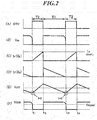
FIG. 2 is a timing chart illustrating the change of signal and voltage at different components of a control IC of the power supply device in the lighting system according to the embodiment. -
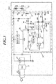
FIG. 3 is a circuit configuration view of a first variation of the LED power supply device according to the embodiment. -
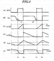
FIG. 4 is a timing chart illustrating the change of signal and voltage at different components of a control IC of the power supply device of the variation. -
FIG. 5 is a circuit configuration view of a second variation of the LED power supply device according to the embodiment. -
FIG. 6 is a circuit configuration view of a third variation of the LED power supply device according to the embodiment. -
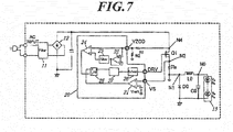
FIG. 7 is a circuit configuration view of a fourth variation of the LED power supply device according to the embodiment. -
FIG. 8A is a circuit configuration view of an exemplary configuration of a lighting power supply device that was considered before the present invention was made. -
FIG. 8B is a circuit configuration view of an exemplary configuration of a lighting power supply device that was considered before the present invention was made. - Hereinafter, a suitable embodiment of the present invention will be described based on the drawings.
-
FIG. 1 illustrates the schematic configuration of an LED power supply device to which the present invention is effectively applied, and an LED lighting system using the LED power supply device. - As illustrated in
FIG. 1 , the LED lighting system of the embodiment, to which an alternating power supply voltage AC is input from a commercial alternating power supply, includes: anoise cutoff filter 11 composed of a common mode coil and the like; arectifier circuit 12 which is composed of a diode bridge, which converts the input alternating current to a direct current by full-wave rectification, and the like; an LEDpower supply circuit 14 which is composed of an DC-DC converter (direct voltage converter circuit) which supplies a desired electric power to anLED lamp 13, which is a load, based on the voltage and current converted by therectifier circuit 12; and the like. TheLED lamp 13 includes an LED array in which LEDs are connected in series. - The LED
power supply circuit 14 of the embodiment includes: an inductor L0, a switching transistor Q1 and a sense resistor Rs for current detection that are connected in series with theLED lamp 13 between an output terminal OUT connected to theLED lamp 13 and a ground point; a rectifier diode D0 connected between a connection node N1 between the inductor L0 and the switching transistor Q1, and the output terminal OUT; a capacitor C0 connected in parallel to theLED lamp 13; a switching control semiconductor integrated circuit (hereinafter referred to as an control IC) 20 that controls the switching transistor Q1 by on/off control; and aregulator 15 that generates a power supply voltage required for the operation of thecontrol IC 20. The LEDpower supply circuit 14 is thus configured as a so-called switching regulator. - When the switching transistor Q1 is turned on, electric current flows from the
rectifier circuit 12 to the transistor Q1 through theLED lamp 13 and the inductor L0 so that theLED lamp 13 emits light and the inductor L0 accumulates an energy. Then, when the switching transistor Q1 is turned off, the energy accumulated in the inductor L0 is released so that electric current flows from the inductor L0 to the output terminal OUT through the rectifier diode D0. By this current, theLED lamp 13 emits light. - In the LED
power supply circuit 14 of the embodiment, the potential at a connection node N2, which is generated by current-to-voltage conversion of the sense resistor Rs, is input to a current detection terminal VS of thecontrol IC 20. Further, resistors R1, R2 are connected in series between the connection node N1 between the inductor L0 and the rectifier diode D0 and a ground point. The potential at a connection node N3 between the resistors R1 and R2 is input to a zero current detection terminal VZCD of thecontrol IC 20. The resistors R1, R2 are provided to divide voltage so that the voltage applied to thecontrol IC 20 does not exceed the withstanding voltage, which can be omitted depending on the withstanding voltage of thecontrol IC 20 or the system configuration. - The
control IC 20 of the embodiment includes: acomparator 21 that compares the input voltage at the current detection terminal VS with a reference voltage Vref1 so as to output a corresponding voltage; avoltage follower 22 which functions as a buffer, to which the voltage at the zero current detection terminal VZCD is input; a smoothingfilter 23 connected to an output terminal of thevoltage follower 22; and acomparator 24 that compares the voltage at the zero current detection terminal VZCD and the voltage smoothed by the smoothingfilter 23 so as to output a corresponding voltage. Thevoltage follower 22 is provided in order to eliminate the influence of the smoothingfilter 23 on the potential at the connection node N3. - The
control IC 20 further includes: an RS flip-flop 25 with a reset terminal and a set terminal to which the output voltage of thecomparator 21 and the output voltage of thecomparator 24 are respectively input; and adriver circuit 26 that generates and outputs a drive signal DRV for the on/off control of the switching transistor Q1 according to the output of the RS flip-flop 25. When the current flowing through the inductor L0 becomes zero, the output voltage of thecomparator 24 is changed to high so that the RS flip-flop 25 is set. Then, the output signal and thus the drive signal DRV output from thedriver circuit 26 are changed to high so that the switching transistor Q1 is turned on. - Further, the control IC is configured to perform a control (peak current control) such that when the current Id flowing through the switching transistor Q1 reaches a predetermined level (which corresponds to Vref1), the output voltage of the
comparator 21 is changed to high and the RS flip-flop 25 is reset. Then, the drive signal DRV is changed to low so that the switching transistor Q1 is turned off. - Between the RS flip-
flop 25 and thedriver circuit 26, alogic circuit 27 may be provided which controls the operation of thedrive circuit 26 by logical operation between the output of the RS flip-flop 25 and the signal for controlling the operation and protecting function of thecontrol IC 20. - While any dimming control system is not illustrated in the
control IC 20 inFIG. 1 , dimming control can be achieved, for example, by a configuration such that a variable voltage supply is provided as a reference voltage supply (Vref1) that is connected to the inverting input terminal of thecomparator 21, and that the voltage of the variable voltage supply is changed according to an external dimming control signal. Another possible configuration is such that a variable resistor (volume) is used as the sense resistor Rs, and that dimming control is achieved by changing the resistance thereof. The zero current detecting method of the present invention is applicable regardless of the dimming method including DC dimming, PWM dimming, phase dimming and the like. - Next, the on/off control operation of the switching transistor Q1 by the
control IC 20 will be described referring to the timing chart ofFIG. 2 . InFIG. 2, (A) is the waveform of the drive signal DRV, which is output from thedriver circuit 26 to control the switching transistor Q1 by on/off control, (B) is the waveform of a drain-source voltage Vds of the switching transistor Q1, (C) is the waveform of the drain current Id of the switching transistor Q1, (D) is the waveform of the current IF through the rectifier diode D0, (E) is the waveform of the current ILED (= Id+IF) flowing through theLED lamp 13, and (F) is the waveform of the voltage at the zero current detection terminal VZCD. - As illustrated in
FIG. 2 , thecontrol IC 20 according to the embodiment operates such that the drain current Id of the switching transistor Q1 as illustrated inFIG. 2 (C) is zero during a period T1 in which the on/off drive signal DRV for the switching transistor Q1 is low so that the transistor Q1 is off, but it starts to increase gradually from a timing t1 when the drive signal DRV is changed to high so that the transistor Q1 is turned on (period T2). When the drain current Id reaches a predetermined value Ip, the transistor Q1 is turned off (timing t2). Then, as illustrated inFIG. 2 (D) , the current IF through the rectifier diode D0 rises sharply and thereafter gradually decreases (period T1). At a timing t3 at which the current IF becomes zero, a resonance would occur if the transistor Q1 was not turned on. In contrast, thecontrol IC 20 of the embodiment, which can detect the timing t3 at which the current IF becomes zero by means of thecomparator 24, sets the RS flip-flop 25 at the detected timing so as to turn on the transistor Q1. - Accordingly, during the period T2 in which the switching transistor Q1 is on, the drain current Id of the switching transistor Q1 gradually increases as illustrated in
FIG. 2 (D) while the current IF through the rectifier diode D0 remains zero as illustrated inFIG. 2 (D) . This current is converted by current-voltage conversion of the sense resistor Rs, and is input to the current detection terminal VS and compared with the reference voltage Vref1 by thecomparator 21. When the voltage at the terminal VS reaches the reference voltage Vref1, the output of thecomparator 21 is changed so that the RS flip-flop 25 is reset. Accordingly, the transistor Q1 is turned off. By repeating the above-described operation, electric current keeps flowing through theLED lamp 13, which is a load, and the light emission is thus maintained. - Furthermore, the
control IC 20 of the embodiment includes the smoothingfilter 23 that is disposed at the zero current detection terminal VZCD to smooth the input voltage of the terminal, and is configured to determine the timing of turning on the switching transistor Q1 by comparing the smoothed voltage VZCDREF with the input voltage at the zero current detection terminal VZCD by means of thecomparator 24. - In this process, the voltage (hereinafter referred to as the one-side voltage) at the terminal N0 opposite the connection node N1 of the inductor L0 is represented by the following equation.

- VIND is the one-side voltage, VIN is the input voltage, and VLED is the voltage applied to the
LED lamp 13. - The voltage VLED applied to the
LED lamp 13 is represented by the following equation.
- Ton is the period in which the switching transistor Q1 is on, and Toff is the period in which the switching transistor Q1 is off. Substituting the equation (2) in the equation (1) yields the following equation.

- It can be understood from the above equation (3) that the one-side voltage VIND of the inductor L0 is the product of the input voltage VIN and the off duty. In contrast, it can be understood from the waveform in
FIG. 2 (F) that the average voltage VZCDREF at the zero current detection terminal VZCD is obtained by flattening the voltage at the zero current detection terminal VZCD during the off period T1. That is, the smoothingfilter 23 of thecontrol IC 20 of the embodiment is equivalent to a pseudo-generator that generates a voltage proportional to the voltage at the terminal of the inductor L0 that is not input to thecontrol IC 20. - From the above description, it can be understood that the configuration of the embodiment enables detection of the timing (t1, t3, ...) at which the current through the inductor L0 becomes zero only by adding the single zero current detection terminal VZCD to the
control IC 20. Further, this configuration is advantageous in that the switching control can follow the fluctuation of the input voltage since the timing at which the current through the inductor L0 becomes zero can be detected correctly even when the input voltage Vin is fluctuating. Furthermore, even when the number of LEDs of theLED lamp 13 is changed, it is not necessary to change the configuration of the circuit. -
FIG. 3 illustrates a first variation of the LEDpower supply circuit 14 inFIG. 1 . - The LED
power supply circuit 14 of the variation includes an external capacitor C3 connected to the zero current detection terminal VZCD of thecontrol IC 20 as illustrated inFIG. 1 so that the plunge of the voltage input to the terminal VZCD is moderated. In this way, the LEDpower supply circuit 14 is configured to turn on the switching transistor Q1 in response to detection of the bottoms b1, b2, ... (timing t1, t3,...) of resonances that are generated after the current reaches zero as illustrated inFIG. 4 instead of the timing at which the current through the inductor L0 becomes zero. - This variation is advantageous in the reduced switching noise and the improved power efficiency compared to the LED power supply circuit in
FIG. 1 since the timing of turning on the switching transistor Q1 can be delayed. -
FIG. 5 to FIG. 7 illustrate second to fourth variations of the LEDpower supply circuit 14 inFIG. 1 . - The LED
power supply circuit 14 of the second variation as illustrated inFIG. 5 is configured as a step-up power supply device in which the rectifier diode D0 is disposed in series with theLED lamp 13, and the inductor L0 is disposed in parallel to them. The power supply circuit as illustrated inFIG. 5 includes an external capacitor C3 connected to the zero current detection terminal VZCD of thecontrol IC 20 and is configured to detect the bottoms of resonances. However, a configuration without the capacitor C3 is also possible as in the LED power supply circuit inFIG. 1 . - The LED
power supply circuit 14 of the third variation as illustrated inFIG. 6 includes a coupling capacitor C4 connected in series with the resistor R1 between the connection node N1 between the inductor L0 and the switching transistor Q1 and the zero current detection terminal VZCD of thecontrol IC 20, and is configured to detect the timing at which the current becomes zero by transmitting the potential change at the connection node N1 to the zero current detection terminal VZCD by means of AC coupling. - The LED
power supply circuit 14 of the fourth variation inFIG. 7 is configured as a high-side driver power supply device (not sink-type but source-type power supply device) in which the rectifier diode D0 is connected in the opposite direction in series with the switching transistor Q1 and the sense resistor Rs, the inductor L0 and theLED lamp 13 are connected in series between the connection node N1 between the sense resistor R2 and the rectifier diode D0 and a ground point, and the capacitor C0 is disposed in parallel to theLED lamp 13. - While the invention made by the present inventor is specifically described based on an embodiment, the present invention is not limited to the above-described embodiment. For example, the embodiment is an example of a DC-DC converter that includes the switching transistor Q1, the rectifier diode D0 and the inductor L0. However, a configuration as a so-called synchronous rectifier switching regulator is also possible in which a transistor is used instead of the rectifier diode D0, and a
control IC 20 monitors the drain-source voltage of the transistor so as to perform the on/off control complementally with the switching transistor Q1. - The present invention is applicable not only to LED lighting power supply devices but also to lighting power supply devices for lighting equipment other than LED lamps and other general non-insulated power supply devices.
-
- 11 Filter
- 12 Rectifier circuit
- 13 LED lamp (lighting equipment)
- 14 LED power supply circuit (lighting power supply device)
- 15 Regulator
- 20 Control IC (control circuit)
- 21, 24 Comparator
- 22 Voltage follower
- 23 Smoothing filter (smoothing circuit)
- 25 RS flip-flop
- 26 Driver circuit
Claims (4)
- A non-insulated power supply device, comprising:a switching element connected in series with a load;an inductor connected in series with or in parallel to the load;a rectification element connected such that a discharge current from the inductor can flow to the load while the switching element is off;a current-voltage conversion element connected in series with the switching element; anda control circuit which controls the switching element by on/off control,wherein the non-insulated power supply device is configured to turn on the switching element so as to allow current to flow to the inductor, and thereafter to turn off the switching element so as to allow the discharge current from the inductor to flow to the rectification element and the load,wherein the control circuit comprises:a first external terminal to which a voltage converted by the current-voltage conversion element is input;a second external terminal to which a voltage at one terminal of the inductor or a voltage proportional to the voltage at the one terminal of the inductor is input;a smoothing circuit which smooths the input voltage to the second external terminal; anda voltage comparison circuit which compares a voltage smoothed by the smoothing circuit with the input voltage to the second external terminal, andwherein based on an output from the voltage comparison circuit, the control circuit switches the switching element from off to on at or near a timing at which a current through the inductor is reduced to zero, and switches the switching element from on to off in response to an input voltage to the first external terminal reaching a predetermined voltage.
- The non-insulated power supply device according to claim 1, wherein the control circuit further comprises a buffer which is disposed between the second external terminal and the smoothing circuit and to which the voltage at the second external terminal is input, and
wherein the smoothing circuit smooths an output voltage from the buffer. - The non-insulated power supply device according to claim 1 or 2, further comprising a dividing means which is disposed between the one terminal of the inductor and the second external terminal and which divides the voltage at the one terminal.
- The non-insulated power supply device according to claim 3, further comprising a capacitor element connected to the second external terminal.
Applications Claiming Priority (2)
| Application Number | Priority Date | Filing Date | Title |
|---|---|---|---|
| JP2014261532A JP6417930B2 (en) | 2014-12-25 | 2014-12-25 | Non-insulated power supply |
| PCT/JP2015/085449 WO2016104345A1 (en) | 2014-12-25 | 2015-12-18 | Non-isolated power supply device |
Publications (2)
| Publication Number | Publication Date |
|---|---|
| EP3240170A1 true EP3240170A1 (en) | 2017-11-01 |
| EP3240170A4 EP3240170A4 (en) | 2018-07-25 |
Family
ID=56150365
Family Applications (1)
| Application Number | Title | Priority Date | Filing Date |
|---|---|---|---|
| EP15872914.5A Withdrawn EP3240170A4 (en) | 2014-12-25 | 2015-12-18 | Non-isolated power supply device |
Country Status (6)
| Country | Link |
|---|---|
| US (1) | US10069398B2 (en) |
| EP (1) | EP3240170A4 (en) |
| JP (1) | JP6417930B2 (en) |
| KR (1) | KR20170099843A (en) |
| CN (1) | CN107112896B (en) |
| WO (1) | WO2016104345A1 (en) |
Cited By (2)
| Publication number | Priority date | Publication date | Assignee | Title |
|---|---|---|---|---|
| US10757767B2 (en) | 2018-10-09 | 2020-08-25 | Lumileds Llc | DC-DC converter circuit configuration |
| US11612031B2 (en) | 2019-03-29 | 2023-03-21 | Lumileds Llc | DC-DC converter circuit configuration |
Families Citing this family (1)
| Publication number | Priority date | Publication date | Assignee | Title |
|---|---|---|---|---|
| DE102019103660B4 (en) * | 2019-02-13 | 2025-09-11 | Vossloh-Schwabe Deutschland Gmbh | Operating circuit for operating multiple loads |
Family Cites Families (20)
| Publication number | Priority date | Publication date | Assignee | Title |
|---|---|---|---|---|
| JPS58194462A (en) * | 1982-05-08 | 1983-11-12 | Minolta Camera Co Ltd | Partial erasing or extracting method for reading original |
| US7579818B2 (en) * | 2005-07-28 | 2009-08-25 | Semiconductor Components Industries, L.L.C. | Current regulator and method therefor |
| JP4963068B2 (en) | 2007-02-06 | 2012-06-27 | 新電元工業株式会社 | Power factor correction circuit |
| US7750616B2 (en) * | 2007-06-21 | 2010-07-06 | Green Mark Technology Inc. | Buck converter LED driver circuit |
| JP5205974B2 (en) * | 2008-01-08 | 2013-06-05 | ミツミ電機株式会社 | DC power supply, LED drive power supply, and power supply control semiconductor integrated circuit |
| US8106597B2 (en) * | 2008-01-22 | 2012-01-31 | Supertex, Inc. | High efficiency boost LED driver with output |
| US8130519B2 (en) * | 2008-11-12 | 2012-03-06 | Supertex, Inc. | Led driver with low harmonic distortion of input AC current and methods of controlling the same |
| US8253395B2 (en) * | 2008-08-07 | 2012-08-28 | Microsemi Corporation | Bus voltage optimizer for switched power converter |
| CN102187736B (en) * | 2008-10-20 | 2013-06-19 | 赤多尼科有限公司 | LED driver circuit |
| US8305004B2 (en) * | 2009-06-09 | 2012-11-06 | Stmicroelectronics, Inc. | Apparatus and method for constant power offline LED driver |
| US8427069B2 (en) * | 2009-06-22 | 2013-04-23 | Polar Semiconductor, Inc. | Current-regulated power supply with soft-start protection |
| KR101948128B1 (en) * | 2010-02-17 | 2019-02-15 | 페어차일드코리아반도체 주식회사 | Control device,led emitting light device comprising the same, and control method |
| CN102014541B (en) * | 2010-05-18 | 2011-12-14 | 凹凸电子(武汉)有限公司 | Light source driving circuit and method for regulating electric power of light source |
| JP2012115074A (en) | 2010-11-26 | 2012-06-14 | Mitsumi Electric Co Ltd | Insulation type power supply device and illumination device |
| JP2012212548A (en) | 2011-03-31 | 2012-11-01 | Mitsumi Electric Co Ltd | Lighting power supply device |
| US8531112B2 (en) * | 2011-05-15 | 2013-09-10 | Green Solution Technology Co., Ltd | LED driving circuit and protecting circuit thereof |
| JP2013165598A (en) | 2012-02-13 | 2013-08-22 | Panasonic Corp | Power supply device and luminaire and lighting fixture using the same |
| US9048752B2 (en) * | 2012-09-27 | 2015-06-02 | Semiconductor Components Industries, Llc | Off-line power converter and integrated circuit suitable for use in same |
| JP6286870B2 (en) * | 2013-05-24 | 2018-03-07 | 三菱電機株式会社 | Lighting device and lighting device |
| JP2014239620A (en) * | 2013-06-10 | 2014-12-18 | ソニー株式会社 | Switching power supply apparatus, switching power supply control method, and electronic apparatus |
-
2014
- 2014-12-25 JP JP2014261532A patent/JP6417930B2/en active Active
-
2015
- 2015-12-18 KR KR1020177011645A patent/KR20170099843A/en not_active Withdrawn
- 2015-12-18 EP EP15872914.5A patent/EP3240170A4/en not_active Withdrawn
- 2015-12-18 WO PCT/JP2015/085449 patent/WO2016104345A1/en not_active Ceased
- 2015-12-18 US US15/537,988 patent/US10069398B2/en active Active
- 2015-12-18 CN CN201580070844.6A patent/CN107112896B/en active Active
Cited By (2)
| Publication number | Priority date | Publication date | Assignee | Title |
|---|---|---|---|---|
| US10757767B2 (en) | 2018-10-09 | 2020-08-25 | Lumileds Llc | DC-DC converter circuit configuration |
| US11612031B2 (en) | 2019-03-29 | 2023-03-21 | Lumileds Llc | DC-DC converter circuit configuration |
Also Published As
| Publication number | Publication date |
|---|---|
| JP2016123195A (en) | 2016-07-07 |
| EP3240170A4 (en) | 2018-07-25 |
| CN107112896A (en) | 2017-08-29 |
| KR20170099843A (en) | 2017-09-01 |
| WO2016104345A1 (en) | 2016-06-30 |
| CN107112896B (en) | 2019-04-12 |
| US20170353100A1 (en) | 2017-12-07 |
| US10069398B2 (en) | 2018-09-04 |
| JP6417930B2 (en) | 2018-11-07 |
Similar Documents
| Publication | Publication Date | Title |
|---|---|---|
| EP2458722B1 (en) | LED driving apparatus | |
| US8614551B2 (en) | SCR dimming circuit and method | |
| US9113519B2 (en) | LED driving apparatus and LED lighting apparatus | |
| US9544962B2 (en) | Driver device and driving method for driving an LED unit | |
| US9313844B2 (en) | Lighting device and luminaire | |
| US8188617B2 (en) | Current balancing apparatus, current balancing method, and power supply apparatus | |
| US9467039B2 (en) | Power supply system with ripple suppression circuit and ripple suppression method thereof | |
| US20150359052A1 (en) | Switched mode power supply | |
| EP3095299B1 (en) | Led driver and control method | |
| CN109392220B (en) | Driver circuits for light-emitting diode devices, lighting equipment and motor vehicles | |
| EP3468308A1 (en) | Light-dimming device | |
| JP2020014325A (en) | Lighting device and light fixture | |
| US9288855B2 (en) | Driving circuit for driving LED load | |
| US10069398B2 (en) | Non-isolated power supply device | |
| US20130099671A1 (en) | Power supply device and driving device | |
| US9408272B2 (en) | Light driver and the controller and driving method thereof | |
| JP5547849B2 (en) | DC power supply circuit | |
| CN103687178B (en) | Driving circuit and related circuit driving method thereof | |
| JP5393744B2 (en) | LED lighting device | |
| US9232577B2 (en) | Power driver for light emitting diode illumination and control method thereof | |
| CN103874276B (en) | Power circuit and lighting device | |
| WO2013172259A1 (en) | Switching power supply circuit and led lighting device | |
| JP2023127378A (en) | Lighting devices and luminaires | |
| JP2015185450A (en) | Power supply device and lighting device | |
| CN104206021B (en) | LED drive circuit with efficiency improvement function |
Legal Events
| Date | Code | Title | Description |
|---|---|---|---|
| PUAI | Public reference made under article 153(3) epc to a published international application that has entered the european phase |
Free format text: ORIGINAL CODE: 0009012 |
|
| 17P | Request for examination filed |
Effective date: 20170621 |
|
| AK | Designated contracting states |
Kind code of ref document: A1 Designated state(s): AL AT BE BG CH CY CZ DE DK EE ES FI FR GB GR HR HU IE IS IT LI LT LU LV MC MK MT NL NO PL PT RO RS SE SI SK SM TR |
|
| AX | Request for extension of the european patent |
Extension state: BA ME |
|
| DAV | Request for validation of the european patent (deleted) | ||
| DAX | Request for extension of the european patent (deleted) | ||
| A4 | Supplementary search report drawn up and despatched |
Effective date: 20180621 |
|
| RIC1 | Information provided on ipc code assigned before grant |
Ipc: H02M 3/156 20060101AFI20180615BHEP Ipc: H02M 1/00 20060101ALN20180615BHEP Ipc: H02M 1/08 20060101ALI20180615BHEP Ipc: H05B 33/08 20060101ALI20180615BHEP |
|
| STAA | Information on the status of an ep patent application or granted ep patent |
Free format text: STATUS: THE APPLICATION IS DEEMED TO BE WITHDRAWN |
|
| 18D | Application deemed to be withdrawn |
Effective date: 20190122 |