EP3240141A1 - Contactless power transmission device and contactless power transmission/reception apparatus - Google Patents
Contactless power transmission device and contactless power transmission/reception apparatus Download PDFInfo
- Publication number
- EP3240141A1 EP3240141A1 EP17166766.0A EP17166766A EP3240141A1 EP 3240141 A1 EP3240141 A1 EP 3240141A1 EP 17166766 A EP17166766 A EP 17166766A EP 3240141 A1 EP3240141 A1 EP 3240141A1
- Authority
- EP
- European Patent Office
- Prior art keywords
- power
- power transmission
- shield
- power reception
- coil
- Prior art date
- Legal status (The legal status is an assumption and is not a legal conclusion. Google has not performed a legal analysis and makes no representation as to the accuracy of the status listed.)
- Granted
Links
Images




Classifications
-
- H—ELECTRICITY
- H02—GENERATION; CONVERSION OR DISTRIBUTION OF ELECTRIC POWER
- H02J—ELECTRIC POWER NETWORKS; CIRCUIT ARRANGEMENTS OR SYSTEMS FOR SUPPLYING OR DISTRIBUTING ELECTRIC POWER; SYSTEMS FOR STORING ELECTRIC ENERGY
- H02J50/00—Circuit arrangements or systems for wireless supply or distribution of electric power
- H02J50/40—Circuit arrangements or systems for wireless supply or distribution of electric power using two or more transmitting or receiving devices
- H02J50/402—Circuit arrangements or systems for wireless supply or distribution of electric power using two or more transmitting or receiving devices the two or more transmitting or the two or more receiving devices being integrated in the same unit, e.g. power mats with several coils or antennas with several sub-antennas
-
- H—ELECTRICITY
- H01—ELECTRIC ELEMENTS
- H01F—MAGNETS; INDUCTANCES; TRANSFORMERS; SELECTION OF MATERIALS FOR THEIR MAGNETIC PROPERTIES
- H01F27/00—Details of transformers or inductances, in general
- H01F27/02—Casings
-
- H—ELECTRICITY
- H01—ELECTRIC ELEMENTS
- H01F—MAGNETS; INDUCTANCES; TRANSFORMERS; SELECTION OF MATERIALS FOR THEIR MAGNETIC PROPERTIES
- H01F27/00—Details of transformers or inductances, in general
- H01F27/34—Special means for preventing or reducing unwanted electric or magnetic effects, e.g. no-load losses, reactive currents, harmonics, oscillations, leakage fields
- H01F27/36—Electric or magnetic shields or screens
- H01F27/363—Electric or magnetic shields or screens made of electrically conductive material
-
- H—ELECTRICITY
- H01—ELECTRIC ELEMENTS
- H01F—MAGNETS; INDUCTANCES; TRANSFORMERS; SELECTION OF MATERIALS FOR THEIR MAGNETIC PROPERTIES
- H01F38/00—Adaptations of transformers or inductances for specific applications or functions
- H01F38/14—Inductive couplings
-
- H—ELECTRICITY
- H02—GENERATION; CONVERSION OR DISTRIBUTION OF ELECTRIC POWER
- H02J—ELECTRIC POWER NETWORKS; CIRCUIT ARRANGEMENTS OR SYSTEMS FOR SUPPLYING OR DISTRIBUTING ELECTRIC POWER; SYSTEMS FOR STORING ELECTRIC ENERGY
- H02J50/00—Circuit arrangements or systems for wireless supply or distribution of electric power
- H02J50/10—Circuit arrangements or systems for wireless supply or distribution of electric power using inductive coupling
-
- H—ELECTRICITY
- H02—GENERATION; CONVERSION OR DISTRIBUTION OF ELECTRIC POWER
- H02J—ELECTRIC POWER NETWORKS; CIRCUIT ARRANGEMENTS OR SYSTEMS FOR SUPPLYING OR DISTRIBUTING ELECTRIC POWER; SYSTEMS FOR STORING ELECTRIC ENERGY
- H02J50/00—Circuit arrangements or systems for wireless supply or distribution of electric power
- H02J50/10—Circuit arrangements or systems for wireless supply or distribution of electric power using inductive coupling
- H02J50/12—Circuit arrangements or systems for wireless supply or distribution of electric power using inductive coupling of the resonant type
-
- H—ELECTRICITY
- H02—GENERATION; CONVERSION OR DISTRIBUTION OF ELECTRIC POWER
- H02J—ELECTRIC POWER NETWORKS; CIRCUIT ARRANGEMENTS OR SYSTEMS FOR SUPPLYING OR DISTRIBUTING ELECTRIC POWER; SYSTEMS FOR STORING ELECTRIC ENERGY
- H02J50/00—Circuit arrangements or systems for wireless supply or distribution of electric power
- H02J50/70—Circuit arrangements or systems for wireless supply or distribution of electric power involving the reduction of electric, magnetic or electromagnetic leakage fields
-
- H—ELECTRICITY
- H02—GENERATION; CONVERSION OR DISTRIBUTION OF ELECTRIC POWER
- H02J—ELECTRIC POWER NETWORKS; CIRCUIT ARRANGEMENTS OR SYSTEMS FOR SUPPLYING OR DISTRIBUTING ELECTRIC POWER; SYSTEMS FOR STORING ELECTRIC ENERGY
- H02J50/00—Circuit arrangements or systems for wireless supply or distribution of electric power
- H02J50/90—Circuit arrangements or systems for wireless supply or distribution of electric power involving detection or optimisation of position, e.g. alignment
-
- H—ELECTRICITY
- H02—GENERATION; CONVERSION OR DISTRIBUTION OF ELECTRIC POWER
- H02J—ELECTRIC POWER NETWORKS; CIRCUIT ARRANGEMENTS OR SYSTEMS FOR SUPPLYING OR DISTRIBUTING ELECTRIC POWER; SYSTEMS FOR STORING ELECTRIC ENERGY
- H02J7/00—Circuit arrangements for charging or discharging batteries or for supplying loads from batteries
- H02J7/50—Circuit arrangements for charging or discharging batteries or for supplying loads from batteries acting upon multiple batteries simultaneously or sequentially
-
- H—ELECTRICITY
- H02—GENERATION; CONVERSION OR DISTRIBUTION OF ELECTRIC POWER
- H02J—ELECTRIC POWER NETWORKS; CIRCUIT ARRANGEMENTS OR SYSTEMS FOR SUPPLYING OR DISTRIBUTING ELECTRIC POWER; SYSTEMS FOR STORING ELECTRIC ENERGY
- H02J7/00—Circuit arrangements for charging or discharging batteries or for supplying loads from batteries
- H02J7/70—Circuit arrangements for charging or discharging batteries or for supplying loads from batteries characterised by the mechanical construction
- H02J7/751—Circuit arrangements for charging or discharging batteries or for supplying loads from batteries characterised by the mechanical construction concerning the insertion or the connection of the batteries
Definitions
- the present invention relates to a power transmission technology in general, and embodiments described herein relate in particular to a power transmission device which transmits power to a power reception device in a contactless manner, and a power transmission/reception apparatus which transmits and receives power in a contactless manner.
- a contactless power transmission device is an apparatus which transmits power to a power reception device such as a portable terminal or a tablet terminal by using electromagnetic coupling such as electromagnetic induction or magnetic field resonance.
- the contactless power transmission device includes a power transmission circuit and a power transmission coil for transmitting power
- the power reception device includes a power reception coil for receiving power, a power reception circuit for using the received power for the drive of own device, a charging circuit for charging a secondary battery mounted in own device, and the like.
- the contactless power transmission device it is required to suppress radiation noise to be low while power is transmitted to the power reception device with a high efficiency. Therefore, as the power transmission circuit of the contactless power transmission device, an amplifier in which switching loss is reduced by zero voltage switching (ZVS) and which uses resonance, such as an E-class amplifier is often used.
- ZVS zero voltage switching
- the ZVS allows switching of switching elements such as a MOSFET in a zero-voltage state, is called soft switching, and has effects of reducing switching loss and implementing a highly efficient power transmission circuit.
- soft switching Compared to hard switching which is a normal switching method, soft switching has advantages that the rising of a voltage or a current becomes gentle and the generation of noise is reduced. However, even in the soft switching, the generation of noise due to the switching of switching elements such as MOSFET cannot be avoided, and therefore, in the contactless power transmission device, the switching noise is a major noise source.
- a rectification circuit such as a full-wave rectification circuit is generally connected to the rear stage of the power reception coil.
- a full-wave rectification circuit in which four rectifier diodes are used and are connected in a bridge type is usually used, but noise which is generated due to rectification of the diodes is great.
- noise which is generated due to rectification of the diodes is great.
- the generation of noise is reduced when using the Schottky barrier diode with a high speed instead of using a general diode.
- the Schottky barrier diode there is no change in that the diode is the noise source.
- the power transmission coil for radiating power is connected to the power transmission circuit
- the power reception coil for receiving power is connected to the power reception circuit
- each coil functions as an antenna. Therefore, if there is a noise source in the power transmission circuit and the power reception circuit, there is a problem in that the power transmission coil or the power reception coil functions as an antenna so as to radiate the noise.
- shielding for example, JP-A-2010-070048 , and JP-A-2012-228150 .
- a contactless power transmission device which transmits power to a power reception device in a contactless manner, the contactless power transmission device comprising:
- the notch is formed in a curved shape at a central portion of the side surfaces of the shield case or the partitioning plates, from the opening portion toward the inner side.
- the power transmission coil is disposed on an inner-side surface of the shield room, which faces the opening portion, so as to be orthogonal to or parallel with an insertion direction of the power reception device.
- the power transmission circuit disposed in each of the plurality of shield rooms is operated based on a clock signal, and clock signals supplied to the adjacent power transmission circuits are synchronized with each other with the phases thereof being inverted.
- the invention also relates to a contactless power transmission/reception apparatus comprising:
- the power reception device includes
- the invention further relates to a contactless power transmission system in which power is transmitted to a power reception device in a contactless manner, the contactless power transmission system comprising:
- the notch means is formed in a curved shape at a central portion of the side surfaces of the shield case or the partitioning plates, from the opening portion toward the inner side.
- the power transmission coil is disposed on an inner-side surface of the shield room, which faces the opening portion, so as to be orthogonal to or parallel with an insertion direction of the power reception device.
- the power transmission circuit disposed in each of the plurality of shield rooms is operated based on a clock signal, and clock signals supplied to the adjacent power transmission circuits are synchronized with each other with the phases thereof being inverted.
- the invention further concerns a system for a contactless power transmission/reception comprising:
- the power reception device includes
- An object of the exemplary embodiment is to provide a contactless power transmission device and a contactless power transmission/reception apparatus which have a shield structure in which noise can be sufficiently reduced and a power reception device can be easily extracted and inserted into the contactless power transmission device including a plurality of power transmission devices.
- a contactless power transmission device which transmits power to a power reception device in a contactless manner, and includes a shield case which has an opening portion at one end portion thereof, and is partitioned into a plurality of shield rooms by partitioning plates; a power transmission circuit which is for transmitting power and is disposed to correspond to each of the plurality of shield rooms; a plurality of power transmission coils which are disposed on the inner side in the plurality of shield rooms when viewed from the opening portion, and transmit AC power from the power transmission circuit to the power reception device; and a notch which is formed on side surfaces of the shield case or the partitioning plates, from the opening portion toward the inner side such that both sides of a rear end portion of the power reception device inserted into the plurality of shield rooms can be held.
- FIG. 1 is a block diagram illustrating a contactless power transmission/reception apparatus 100 according to the embodiment.
- the contactless power transmission/reception apparatus 100 includes a plurality of power transmission devices 10A to 10C which transmit power, and a plurality of power reception devices 20A to 20C which receive the transmitted power in a contactless manner.
- the power transmission device may be provided by two or more.
- the power reception device is not necessary that the power reception device is provided by the same number as the power transmission device, and may be provided by one or plural. For example, in a case where three power transmission devices are provided, it is possible to transmit power to three power reception devices at one time.
- the same reference numeral is given to the same circuit part of the power transmission devices 10A, 10B, and 10C.
- the same reference numeral is given to the same circuit part of the power reception devices 20A, 20B, and 20C.
- the power transmission device 10A includes a power transmission coil 11, and the power reception device 20A includes a power reception coil 21. Power output from the power transmission device 10A is transmitted to the power reception device 20A by using electromagnetic coupling such as electromagnetic induction or magnetic field resonance between the power transmission coil 11 and the power reception coil 21.
- the power transmission device 10A includes a power transmission circuit 14 which generates transmission power required for the power transmission, and a control unit 15 which controls the power transmission circuit 14.
- the control unit 15 includes an oscillation circuit 16 and a microprocessor unit (MPU) 17.
- the oscillation circuit 16 supplies frequencies of power carrier waves to the power transmission circuit 14.
- the MPU 17 performs a drive control which causes the power transmission circuit 14 to be operated or stopped according to the necessity, a communication control with respect to the power reception device 20A, and the like.
- the power transmission circuit 14 an amplifier circuit by a switching circuit in which the efficiency is considered to be important, for example, a D-class amplifier circuit or an E-class amplifier circuit is used.
- a MOS-FET is generally used.
- the power transmission circuit 14 performs soft switching by zero voltage switching (ZVS) or zero current switching (ZCS). By performing soft switching, switching loss is reduced, and switching noise and radiation noise can be reduced.
- ZVS zero voltage switching
- ZCS zero current switching
- the oscillating frequency of the oscillation circuit 16 that is, the switching frequency of the power transmission circuit 14 for example, a frequency of 6.78 MHz is used.
- the output of the power transmission circuit 14 is supplied to the power transmission coil 11 through a resonance capacitor 18, and power of power transmission frequency of 6.78 MHz is transmitted from the power transmission coil 11.
- the power transmission frequency of 6.78 MHz is described as an example, but the power transmission frequency is not limited to 6.78 MHz, and may be other frequencies.
- the power transmission devices 10B and 10C have the same circuit configuration as the power transmission device 10A, and DC power is supplied from the AC adaptor 13 to the power transmission devices 10B and 10C.
- switches 19B and 19C may be respectively provided between the AC adaptor 13 and the power transmission device 10B, and between the AC adaptor 13 and the power transmission device 10C. By providing the switches 19B and 19C, it is possible to supply DC power to the power transmission devices 10B and 10C as necessary, and thus if there is no need to operate the power transmission devices 10B and 10C, the switches 19B and 19C may be turned off.
- the power reception device 20A includes a resonance circuit configured of the power reception coil 21 and a resonance capacitor 22, a rectification circuit 23, a voltage conversion circuit 24, and a load circuit 25.
- AC power transmitted through the resonance circuit configured of the power reception coil 21 and the resonance capacitor 22 is converted to a DC voltage by the rectification circuit 23 (for example, a diode full-wave rectification circuit).
- the converted DC voltage is converted, by the voltage conversion circuit 24, to a proper voltage by which the load circuit 25 can be operated.
- the resonance capacitor 22, the rectification circuit 23, and the voltage conversion circuit 24 configure a power reception circuit which converts AC power received by the power reception coil to DC power.
- the load circuit 25 for example, is a circuit of electronic equipment such as a portable terminal or a tablet terminal, and includes a control unit 26, a charging unit 27 and a secondary battery 28. Power received by the power reception device 20 is used for charging the secondary battery 28 built in the electronic equipment, or the like.
- the control unit 26 is configured of a microcomputer including a CPU, and controls the charging unit 27 so that the charging of the secondary battery 28 is appropriately controlled. In addition, the control unit 26 controls the communication with respect to the power transmission device 10A.
- the power reception devices 20B and 20C have the same circuit configuration as the power reception device 20A. Power output from the power transmission devices 10B and 10C is transmitted to the power reception devices 20B and 20C by using electromagnetic coupling such as electromagnetic induction or magnetic field resonance between the corresponding power transmission coil 11 and the corresponding power reception coil 21.
- the switching element such as a MOS-FET used in the power transmission circuit 14 of each of the power transmission devices 10A to 10C performs switching at a high frequency of 6.78 MHz, and thus generates a frequency of 6.78 MHz and harmonic frequencies of 6.78MHz.
- noise can be reduced, but the noise which is not sufficiently reduced is radiated from the power transmission coil 11, or a cable which connects the plug 12 to the AC adaptor 13.
- the rectification circuit 23 of each of the power reception devices 20A to 20C is the major noise source.
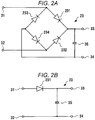
- the rectification circuit 23 for example, a bridge-type full-wave rectification circuit as illustrated in FIG. 2A or a half-wave rectification circuit as illustrated in FIG. 2B is used.
- the full-wave rectification circuit 23 in FIG. 2A is configured of diodes 231 to 234, the anode of the diode 231 and the cathode of the diode 233 are connected to one input port 31 of the full-wave rectification circuit 23, the anode of the diode 232 and the cathode of the diode 234 are connected to the other input port 32.
- cathodes of the diode 231 and the diode 232 are connected to an output port 33, and anodes of the diode 233 and the diode 234 are connected to a reference potential port 34 (earth port).
- a smoothing capacitor 35 is connected between the output port 33 and the reference potential port 34 (earth port), and a DC voltage is obtained from both ends of the smoothing capacitor 35.
- the anode of the diode 231 is connected to the input port 31, and the cathode of the diode 231 is connected to the output port 33.
- the smoothing capacitor 35 is connected between the output port 33 and the reference potential port 34 (earth), and a DC voltage is obtained from both ends of the smoothing capacitor 35.
- the Schottky barrier diode in which the forward voltage drop is small is used, and thus it is possible to improve the rectifying efficiency.
- an electrolytic capacitor or a ceramic capacitor is used as the smoothing capacitor 35 connected to the output port 33 of the rectification circuit 23.
- the noise accompanied by the rectification of the diode may not be removed by the smoothing capacitor 35 only. Therefore, by connecting the low pass filter to the rear stage of the rectification circuit 23, it is possible to reduce noise. Even in such a case, noise is transferred to the power reception coil 21 connected to the input port 31, and is radiated from the power reception coil 21.
- the noise radiated from the contactless power transmission device necessarily satisfies a regulation value stipulated by the Radio Act of each country. In case of Japan, the regulation value of the radiation noise is stipulated by the Radio Act. In addition, if 6.78 MHz as the industry-science-medical (ISM) frequency is used as the power transmission frequency, the restriction target is under the CISPR 11 as the International Standards and the FCC Part 18 in USA. In addition to the noise radiated to the space, noise conducting the power supply line is also regulated.
- ISM industry-science-medical
- the entirety of small equipment such as a portable terminal or portable equipment is input in the shield box, and a shielding door is provided to the shield box may be considered, but in this case, it is necessary to open and close the door of the shield box for extracting and inserting the equipment, which becomes complicated.
- the shield device itself is increased in size.
- a case in which a shielding door is not provided, the depth of the shield box is lengthened, and the power reception device (portable terminal or portable equipment) is accommodated in the shield box sufficiently is also considered.
- the power reception device is accommodated in the shield case of which the depth is lengthened, the effect of reducing radiation noise is improved, but there is a problem that it is difficult to extract the power reception device from the shield case.
- the contactless power transmission device is provided in which the power transmission devices 10A to 10C and the power reception devices 20A to 20C are covered by a case (shield case) having shielding effects, the power reception devices 20A to 20C can be extracted through the opening portion of the shield case, the opening area of the shield case is reduced as much as possible, and thus the power reception devices 20A to 20C are easily extracted and inserted.
- a case shield case having shielding effects
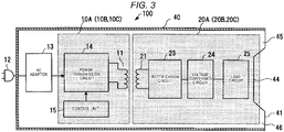
- FIG. 3 is a configuration diagram schematically illustrating the contactless power transmission device according to the embodiment.
- the power transmission device 10A including the power transmission coil 11 is provided in a shield case 40. Since the power transmission devices 10B and 10C also have the same configuration as the power transmission device 10A, the power transmission device 10A is representatively described.
- the shield case 40 includes an opening portion 41 at one end portion thereof, and the power reception device 20A can be accommodated in the shield case 40 through the opening portion 41.
- FIG. 3 a case in which the AC adaptor 13 is included in the power transmission device 10 is illustrated, but the AC adaptor 13 can be configured as a separate circuit component.
- a configuration in which only the AC adaptor 13 is provided to the outside of the shield case 40 may be adopted.
- the power transmission coil 11 is attached to the inner side of the shield case 40 when viewed from the opening portion 41.
- the power reception coil 21 is disposed at a position facing the power transmission coil 11, and when the power reception device 20A is accommodated in the shield case 40, the power transmission coil 11 and the power reception coil 21 become close to each other so that power can be transmitted.
- the size of the inner circumference of the shield case 40 is set to be slightly greater than that of the outer circumference of the power reception device 20A such that the efficiency of transmitting power does not deteriorate due to the deviation in the position, at which the power transmission coil 11 and the power reception coil 21 face each other, being increased.
- the gap between the outer circumference of the power reception device 20A and the inner circumference of the shield case 40 is within about 2 to 3 cm, and thus even if the position of the power reception device 20A is deviated in the shield case 40, the deviation is minimized.
- the power transmission coil 11 is provided in the shield case 40, but the circuit part configuring the power transmission device 10A except for the power transmission coil 11 may be disposed in the same shield case 40, and may be integrally disposed to the outside of the shield case 40 so as to correspond to the shield case 40.
- a countermeasure for noise such as inserting the circuit part into a shield case separate from the shield case 40, is necessary so that noise is not radiated.
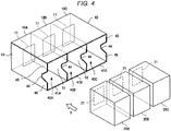
- FIG. 4 is a perspective view illustrating the power transmission devices 10A to 10C and the power reception devices 20A to 20C of the embodiment.
- the power transmission devices 10A, 10B, and 10C are configured to be in the shield case 40.
- the shield case 40 has a box shape, and is partitioned into three shield rooms 40A, 40B, and 40C by partitioning plates 51 and 52.
- the partitioning plates 51 and 52 are configured of metal or conductive members which have shielding effects similar to the shield case 40, and the shield rooms 40A, 40B, and 40C which are plurally partitioned by these partitioning plates 51 and 52 are formed.
- the power reception devices 20A, 20B, and 20C can be respectively extracted from and inserted into the shield rooms 40A, 40B, and 40C through the opening portions 41A, 41B, and 41C.
- the power transmission device 10A is described as an example, if an insertion direction of the power reception device 20A is set as an arrow X direction, the power transmission coil 11 is attached to the inner side of the shield room 40A which faces the opening portion 41A, in a direction orthogonal to the insertion direction X (vertically).
- the power transmission coil 11 may be formed on a printed circuit board or formed by wirings.
- the circuit part of the power transmission device 10A except for the power transmission coil 11 may be disposed between the power transmission coil 11 and an inner-side end surface 43 of the shield room 40A.
- the power reception coil 21 is disposed at a position facing the power transmission coil 11. If the power reception device 20A is inserted into the shield room 40A in a depth direction through the opening portion 41A, and is inserted up to a position where the power reception device bumps into the power transmission coil 11, the power transmission coil 11 and the power reception coil 21 face each other at a close range within 2 to 3 cm, and power can be transmitted in a contactless manner.
- Notches 44 are formed on both side surfaces of the shield case 40, from the opening portions 41A and 41C toward the inner side, and similarly, the notches 44 are formed on the partitioning plates 51 and 52. That is, the notches 44 are almost formed at the central portion of both sides of the power reception device 20A in the insertion direction X, that is, both side surfaces of the shield room 40A except for the bottom surface portion and the ceiling portion.
- the power reception devices 20A, 20B, and 20C which are respectively inserted into the shield rooms 40A, 40B, and 40C are extracted, due to the notches 44 being provided, the power reception devices 20A, 20B, and 20C are easily extracted.
- the front end portion of the power reception device 20A in the insertion direction faces the power transmission coil 11.
- the rear end portion of the power reception device 20A in the insertion direction is positioned further on the inner side than the opening portion 41A, but a part of the rear end portion is exposed through the notch 44.
- FIG. 5 is a perspective view schematically illustrating a state in which the power reception devices 20A, 20B, and 20C are accommodated in the shield rooms 40A, 40B, and 40C.
- the power reception devices 20A, 20B, and 20C are inserted into the shield rooms 40A, 40B, and 40C, and pushed up to a position where the power reception devices bump into the power transmission coils 11, the power reception coil 21 and the power transmission coil 11 closely face each other. Accordingly, power can be transmitted from the power transmission device 10A to the power reception device 20A in a contactless manner.
- power can be transmitted from the power transmission device 10B to the power reception device 20B, and from the power transmission device 10C to the power reception device 20C in a contactless manner.
- the rear end portions of the power reception devices 20A, 20B, and 20C are positioned further on the inner side than the opening portions 41A, 41B, and 41C, but a part of each rear end portion is exposed through the notch 44.
- the power reception devices 20A, 20B, and 20C are extracted from the shield rooms 40A, 40B, and 40C, if the power reception devices 20A, 20B, and 20C are extracted by the rear end portions thereof being held by fingers from both sides of the notch 44, the power reception devices 20A, 20B, and 20C can be easily extracted.
- FIGS. 6A and 6B are sectional views each illustrating another shape of the notch 44 formed on the shield case 40 and the partitioning plates 51 and 52. That is, in the examples of FIGS. 4 and 5 , the notch 44 has a linear shape (trapezoidal shape), but the notch 44 may be formed in a curved shape such as a semicircular shape as illustrated in FIG. 6A .
- FIG. 6B another shape of the notch 44 formed on the shield case 40 and the partitioning plates 51 and 52, as illustrated in FIG. 6B , one of the protrusions 45 and 46 is provided and the other one is not provided.
- the protrusion 46 is only provided, and thus the notch 44 is formed from the central portion to the other end portion.
- the power reception device 20 can be further easily extracted and inserted.
- the level of radiation noise is slightly increased compared to a case where the protrusions 45 and 46 are provided on both end portions, if there is margin for the regulation value of the noise, the above-described example can be adopted.
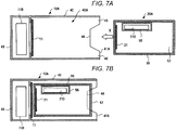
- FIGS. 7A and 7B are sectional views illustrating examples of the power transmission device 10A provided in the shield room 40A, and the power reception device 20A.
- FIG. 7A illustrates a state in which the power reception device 20A is separated from the shield room 40A
- FIG. 7B illustrates a state in which the power reception device 20A is accommodated in the shield room 40A.
- the shield room 40A has a box shape, and the power reception device 20A can be extracted and inserted through the opening portion 41A.
- the power transmission coil 11 is attached to the inner side of the shield room 40A which faces the opening portion 41A, in a direction orthogonal to the insertion direction X (vertically).
- the power transmission coil 11 is a printed coil formed on the printed circuit board.
- a circuit part 110 of the power transmission device 10A except for the power transmission coil 11 is disposed on the outer side of the power transmission coil 11, that is, between the power transmission coil 11 and the inner-side end surface 43 of the shield room 40A.
- the notch 44 is formed on the side surfaces of the shield room 40A, from the edges of the opening portion 41A toward the inner side.
- the power reception device 20A includes a housing 55 of a shape so as to be accommodated in the shield room 40A, and the power reception coil 21 is attached to a surface in the housing 55 which faces the power transmission coil 11.
- a power reception circuit 210 such as the rectification circuit 23 of the power reception device 20A except for the power reception coil 21 is disposed in a shield case 56 provided in the housing 55.
- the shield case 56 and the power reception circuit 210 are provided on the ceiling portion or the bottom surface portion of the housing 55.
- FIGS. 7A and 7B illustrate a case where those are provided on the ceiling portion.
- the power reception device 20A is inserted into the shield room 40A through the opening portion 41A, and is accommodated up to a position where the power reception device bumps into the power transmission coil 11, the power transmission coil 11 and the power reception coil 21 face each other at a close range within 2 to 3 cm, and power can be transmitted in a contactless manner.
- a rear end portion 57 of the power reception device 20A (the housing 55) is positioned further on the inner side than the opening portion 41A, and the rear end portion 57 is exposed through the notch 44. Accordingly, when the power reception device 20A is extracted from the shield room 40A, if the power reception device 20A is extracted by the rear end portion 57 being held by fingers from both sides of the notch 44, the power reception device 20A can be easily extracted.
- the power transmission coil 11 is provided to be along the inner-side surface of the shield room 40A
- the power transmission coil 11 may be provided to be along another surface in the shield room 40A, for example, the bottom surface portion, the ceiling portion, or the side surface portion.
- the power transmission coil may be provided on two or more surfaces.
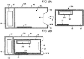
- FIGS. 8A and 8B are sectional views illustrating other examples of the power transmission device 10A provided in the shield room 40A, and the power reception device 20A.
- FIG. 8A illustrates a state in which the power reception device 20A is separated from the shield room 40A
- FIG. 8B illustrates a state in which the power reception device 20A is accommodated in the shield room 40A.
- FIGS. 7A and 7B The main difference point from FIGS. 7A and 7B is that, as illustrated in FIG. 8A , the power transmission coil 11 is attached to the bottom surface portion on the inner side of the shield room 40A when viewed from the opening portion 41 A, to be parallel with the insertion direction X of the power reception device 20A.
- a separate shield case 47 is integrally provided to the outer side of the shield room 40A, and the circuit part 110 of the power transmission device 10A except for the power transmission coil 11 is disposed in the shield case 47. That is, the circuit part except for the power transmission coil 11 is disposed to correspond to the shield room 40A.
- the power reception coil 21 is attached to a position (bottom surface) in the housing 55 which faces the power transmission coil 11.
- the power reception circuit 210 such as the rectification circuit 23 of the power reception device 20A except for the power reception coil 21 is disposed in the shield case 56 provided in the housing 55, and the shield case 56 and the power reception circuit 210 are provided on the ceiling portion or the bottom surface portion of the housing 55.
- the power transmission coil 11 and the power reception coil 21 face each other at a close range within 2 to 3 cm, and power can be transmitted in a contactless manner.
- the power reception device 20A when the power reception device 20A is accommodated in the shield room 40A, a part of the rear end portion 57 is exposed through the notch 44. Accordingly, when the power reception device 20A is extracted from the shield room 40A, if the power reception device 20A is extracted by the rear end portion 57 being held by fingers from both sides of the notch 44, the power reception device 20A can be easily extracted.
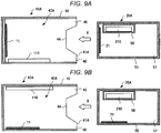
- FIGS. 9A and 9B are sectional views illustrating other examples of the power transmission device 10A provided in the shield room 40A, and the power reception device 20A.
- FIGS. 9A and 9B illustrate a state in which the power reception device 20A is separated from the shield room 40A.
- the power transmission coil 11 is attached to the inner side of the shield room 40A which faces the opening portion 41A, in a direction orthogonal to the insertion direction X (vertically).
- the circuit part 110 of the power transmission device 10A except for the power transmission coil 11 is disposed on the bottom surface portion on the inner side of the shield room 40A.
- the power reception coil 21 is attached to a surface in the housing 55 which faces the power transmission coil 11.
- the power reception circuit 210 such as the rectification circuit 23 of the power reception device 20A except for the power reception coil 21 is disposed in the shield case 56 provided in the housing 55, and the shield case 56 and the power reception circuit 210 are provided on the ceiling portion or the bottom surface portion of the housing 55.
- the power transmission coil 11 and the power reception coil 21 face each other at a close range within 2 to 3 cm, and power can be transmitted in a contactless manner.
- a part of the rear end portion 57 is exposed through the notch 44.
- the power transmission coil 11 is attached to the bottom surface portion on the inner side of the shield room 40A which faces the opening portion 41A, to be parallel with the insertion direction X (horizontally).
- the circuit part 110 of the power transmission device 10A except for the power transmission coil 11 is disposed on the ceiling portion on the inner side of the shield room 40A which faces the opening portion 41A.
- the power reception coil 21 is attached to the bottom surface portion in the housing 55 which face the power transmission coil 11.
- the power reception circuit 210 such as the rectification circuit 23 of the power reception device 20A except for the power reception coil 21 is disposed in the shield case 56 provided in the housing 55, and the shield case 56 and the power reception circuit 210 are provided on the ceiling portion or the bottom surface portion of the housing 55.
- the power transmission coil 11 and the power reception coil 21 face each other at a close range within 2 to 3 cm, and power can be transmitted in a contactless manner.
- a part of the rear end portion 57 of the power reception device 20A is exposed through the notch 44.
- a guide member which guides the power reception device 20A into the shield room 40A may be provided such that when the power reception device 20A is inserted into the shield room 40A, the power reception device 20A does not collide with the circuit part 110. It is preferable that the size of the inner circumference of the shield room 40A is slightly greater than the outer circumference of the power reception device 20A in consideration that the circuit part 110 is equipped in the shield room.
- FIGS. 7A to 9B the configurations of the power transmission device 10A and the power reception device 20A are representatively described, but the power transmission devices 10B and 10C and the power reception devices 20B and 20C have the same configurations.
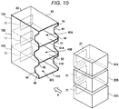
- FIG. 10 is a perspective view illustrating a modification example of the contactless power transmission device according to the embodiment.
- the shield case 40 is of a vertical type.
- the shield case 40 has a box shape, and the shield case 40 is partitioned into three shield rooms 40A, 40B, and 40C in a vertical direction by the partitioning plates 51 and 52 which are disposed in the shield case 40 in a horizontal direction.
- the partitioning plates 51 and 52 are configured of metal or conductive members which have shielding effects similar to the shield case 40, and the shield rooms 40A, 40B, and 40C which are plurally partitioned by these partitioning plates 51 and 52 are formed.
- the power transmission devices 10A, 10B, and 10C are configured to be in the shield rooms 40A to 40C.
- the power transmission coil 11 is attached to the inner side of each of the shield rooms 40A to 40C, in a direction orthogonal to the insertion direction X.
- the circuit part except for the power transmission coil 11 is disposed between the power transmission coil 11 and the inner-side end surface 43 of each of the shield rooms 40A to 40C.
- the notches 44 are formed on both side surfaces of each of the shield rooms 40A to 40C of the shield case 40, from the edges of the opening portions 41 A to 41C toward the inner side so that the power reception devices 20A to 20C are easily extracted. In the example of FIG. 10 , it is not necessary to form the notch on the partitioning plates 51 and 52.
- the notch 44 formed on the shield case 40 may have other shapes.
- FIG. 11 is a perspective view illustrating another modification example of the contactless power transmission device according to the embodiment.
- the shield case 40 is set to face upward, and the power reception devices 20A to 20C are inserted into the shield case 40 from above the shield case (in Y direction) to be accommodated.
- the shield case 40 has the same configuration as that in Fig. 4 except that by causing the shield case 40 to face upward, the power reception devices 20A to 20C are extracted upward from the shield case 40 and inserted into the shield case 40 from above the shield case 40, and thus the detailed description will not be provided.
- the power reception devices 20A to 20C are inserted into the shield rooms 40A to 40C through the opening portions 41 A to 41C, and are inserted up to a position where the power reception devices bump into the power transmission coils 11, the power transmission coil 11 and the power reception coil 21 face each other at a close range within 2 to 3 cm, and power can be transmitted in a contactless manner.
- the power reception devices 20A to 20C are extracted from the shield rooms 40A to 40C, since the notch 44 is provided, the power reception devices 20A to 20C can be easily extracted, In addition, the notch 44 may have other shapes.
- FIG. 12 is a perspective view illustrating still another modification example of the contactless power transmission device according to the embodiment.
- the shield case 40 has a box shape, and is partitioned into four shield rooms 40A to 40D by partitioning plates 51 to 54 that are assembled in a cross shape.
- the partitioning plates 51 to 54 are configured of metal or conductive members which have shielding effects similar to the shield case 40, and the shield rooms 40A to 40D which are plurally partitioned by these partitioning plates 51 to 54 are formed.
- the power transmission devices 10A and 10B are configured to be in the upper shield rooms 40A and 40B, and the power transmission devices 10C and 10D are configured to be in the lower shield rooms 40C and 40D.
- Power reception devices 20A to 20D can respectively be extracted from and inserted into the shield rooms 40A to 40D through opening portions 41A to 41D.
- the power transmission device 10A is described as an example, if the insertion direction of the power reception device 20A is set as an arrow X direction, the power transmission coil 11 is attached to the inner side of the shield room 40A which faces the opening portion 41A, in a direction orthogonal to the insertion direction X.
- the circuit part of the power transmission device 10A except for the power transmission coil 11 may be disposed between the power transmission coil 11 and the inner-side end surface 43 of the shield room 40A.
- the notches 44 are formed on the side surfaces of the shield case 40, from the edges of the opening portions 41A to 41D toward the inner side, and similarly, the notches 44 are formed on the partitioning plates 53 and 54. Accordingly, in a case where the power reception devices 20A to 20D which are respectively inserted into the shield rooms 40A to 40D are extracted, due to the notches 44 being provided, the power reception devices 20A to 20D can be easily extracted.
- the power transmission device 10A to 10D, and the power reception devices 20A to 20D illustrated in FIGS. 10 to 12 may adopt any configuration of FIGS. 7A to 9B .
- the contactless power transmission device including a plurality of power transmission devices
- radiation noise can be sufficiently reduced, and the power reception device can be easily extracted and inserted. Therefore, it is possible to provide a device suitable for portable equipment.
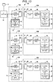
- FIG. 13 is a block diagram illustrating the configuration of the contactless power transmission/reception apparatus 100 according to the second embodiment.
- the contactless power transmission/reception apparatus 100 of FIG. 13 includes a plurality of power transmission devices 10A to 10C which transmit power, and a plurality of power reception devices 20A to 20C which receive the transmitted power in a contactless manner.
- DC power is supplied from the AC adaptor 13 to each of the power transmission devices 10A to 10C.
- the power transmission devices 10A to 10C each have the power transmission circuit 14 and the control unit 15, the control unit 15 includes the oscillation circuit 16 and the MPU 17, and power is transmitted from the power transmission coil 11.
- the power reception devices 20A to 20C each have a resonance circuit configured of the power reception coil 21 and the resonance capacitor 22, the rectification circuit 23, the voltage conversion circuit 24, and the load circuit 25. Power is transmitted to the power reception devices 20A to 20C by using electromagnetic coupling such as electromagnetic induction or magnetic field resonance between the power transmission coil 11 and the power reception coil 21.
- the control unit 15 of the power transmission device 10B includes an inverter 161
- the control unit 15 of the power transmission device 10C includes a buffer 162.
- a clock signal output from the oscillation circuit 16 of the power transmission device 10A is input to the inverter 161, and the clock signal of which the phase is inverted by the inverter 161 is supplied to the power transmission circuit 14.
- the power transmission circuit 14 of the power transmission device 10B performs switching according to a signal of which the phase is inverted with respect to the clock signal output from the oscillation circuit 16 of the power transmission device 10A. Therefore, the phases of AC power output from the power transmission coils 11 of the power transmission device 10A and the power transmission device 10B are inverted from each other.
- a clock signal, which has the same phase, output from the oscillation circuit 16 of the power transmission device 10A is input to the buffer 162. Accordingly, the power transmission circuit 14 of the power transmission device 10C performs switching according to a signal which has the same phase and is synchronized with the clock signal output from the oscillation circuit 16 of the power transmission device 10A. Therefore, the phases of AC power output from the power transmission coils 11 of the power transmission device 10A and the power transmission device 10C are the same and synchronized with each other.
- the volume of the electromagnetic waves radiated from the power transmission coil 11 of the power transmission device 10C may only be considered.
- the electromagnetic waves radiated from the power transmission coil 11 of each of three power transmission devices 10A to 10C interfere with each other, and are affected by the reflection in a space, and thus the state in which the electromagnetic waves are canceled cannot be simply calculated.
- the amount of the electromagnetic waves radiated from one power transmission coil, among three power transmission coils may be simply considered.
- the inverter 161 is configured to be a buffer, and the AC power output from the power transmission coil 11 of each of the power transmission devices 10A to 10C which has the same phase is synchronously output, the electromagnetic waves output from three power transmission coils 11 are superimposed so as to have a volume which is always about three times the volume when the electromagnetic waves are output from one power transmission coil 11.
- FIG. 13 a case in which three power transmission devices 10A to 10C and three power reception devices 20A to 20C are provided is described, but the number of each of power transmission devices and power reception devices may be even, for example, two or four. If the number of power transmission devices is even, by configuring the electromagnetic waves radiated from adjacent power transmission coils to be just canceled, it is possible to further reduce the amount of radiated electromagnetic waves compared to a case where the number of power transmission devices is odd.
- the phases of the AC power output from the power transmission coils of the adjacent power transmission devices are inverted from each other.
- the switches 19B and 19C as illustrated in FIG. 1 may be provided between the AC adaptor 13 and the power transmission device 10B, and between the AC adaptor 13 and the power transmission device 10C.
- the switches 19B and 19C it is possible to supply DC power to the power transmission devices 10B and 10C as necessary, and thus if there is no need to operate the power transmission devices 10B and 10C, the switches 19B and 19C may be turned off.
- the contactless power transmission device including a plurality of power transmission devices
- radiation noise can be further sufficiently reduced, and the power reception device can be easily extracted and inserted.
Landscapes
- Engineering & Computer Science (AREA)
- Power Engineering (AREA)
- Computer Networks & Wireless Communication (AREA)
- Physics & Mathematics (AREA)
- Electromagnetism (AREA)
- Charge And Discharge Circuits For Batteries Or The Like (AREA)
- Rectifiers (AREA)
Abstract
Description
- The present invention relates to a power transmission technology in general, and embodiments described herein relate in particular to a power transmission device which transmits power to a power reception device in a contactless manner, and a power transmission/reception apparatus which transmits and receives power in a contactless manner.
- In recent years, power transmission devices, which transmit power in a contactless manner, spread. A contactless power transmission device is an apparatus which transmits power to a power reception device such as a portable terminal or a tablet terminal by using electromagnetic coupling such as electromagnetic induction or magnetic field resonance. The contactless power transmission device includes a power transmission circuit and a power transmission coil for transmitting power, and the power reception device includes a power reception coil for receiving power, a power reception circuit for using the received power for the drive of own device, a charging circuit for charging a secondary battery mounted in own device, and the like.
- In the contactless power transmission device, it is required to suppress radiation noise to be low while power is transmitted to the power reception device with a high efficiency. Therefore, as the power transmission circuit of the contactless power transmission device, an amplifier in which switching loss is reduced by zero voltage switching (ZVS) and which uses resonance, such as an E-class amplifier is often used. The ZVS allows switching of switching elements such as a MOSFET in a zero-voltage state, is called soft switching, and has effects of reducing switching loss and implementing a highly efficient power transmission circuit.
- Compared to hard switching which is a normal switching method, soft switching has advantages that the rising of a voltage or a current becomes gentle and the generation of noise is reduced. However, even in the soft switching, the generation of noise due to the switching of switching elements such as MOSFET cannot be avoided, and therefore, in the contactless power transmission device, the switching noise is a major noise source.
- Meanwhile, in the power reception device, in order to convert AC power which is received by the power reception coil, to DC power, a rectification circuit such as a full-wave rectification circuit is generally connected to the rear stage of the power reception coil. A full-wave rectification circuit in which four rectifier diodes are used and are connected in a bridge type is usually used, but noise which is generated due to rectification of the diodes is great. In addition, it is known that the generation of noise is reduced when using the Schottky barrier diode with a high speed instead of using a general diode. However, even when using the Schottky barrier diode, there is no change in that the diode is the noise source.
- The power transmission coil for radiating power is connected to the power transmission circuit, the power reception coil for receiving power is connected to the power reception circuit, and each coil functions as an antenna. Therefore, if there is a noise source in the power transmission circuit and the power reception circuit, there is a problem in that the power transmission coil or the power reception coil functions as an antenna so as to radiate the noise. In order to realize low-noise by solving such a problem, techniques regarding shielding (for example,
JP-A-2010-070048 JP-A-2012-228150 - However, in the technique described in
JP-A-2010-070048 JP-A-2012-228150 - To solve such problems, there is provided a contactless power transmission device which transmits power to a power reception device in a contactless manner, the contactless power transmission device comprising:
- a shield case which has an opening portion at one end portion thereof, and is partitioned into a plurality of shield rooms by partitioning plates;
- a power transmission circuit which is for transmitting power and is disposed to correspond to each of the plurality of shield rooms;
- a plurality of power transmission coils which are disposed on the inner side in the plurality of shield rooms when viewed from the opening portion, and transmit AC power from the power transmission circuit to the power reception device; and
- a notch which is formed on side surfaces of the shield case or the partitioning plates, from the opening portion toward the inner side such that both sides of a rear end portion of the power reception device inserted into the plurality of shield rooms can be held.
- Preferably, the notch is formed in a curved shape at a central portion of the side surfaces of the shield case or the partitioning plates, from the opening portion toward the inner side.
- Preferably still, the power transmission coil is disposed on an inner-side surface of the shield room, which faces the opening portion, so as to be orthogonal to or parallel with an insertion direction of the power reception device.
- Preferably yet, the power transmission circuit disposed in each of the plurality of shield rooms is operated based on a clock signal, and clock signals supplied to the adjacent power transmission circuits are synchronized with each other with the phases thereof being inverted.
- The invention also relates to a contactless power transmission/reception apparatus comprising:
- a power reception device; and
- the power transmission device as defined above, the power transmission device transmitting power to the power reception device in a contactless manner.
- Preferably, the power reception device includes
- a housing which can be accommodated in any of the plurality of shield rooms,
- a power reception coil which is disposed in the housing so as to face the power transmission coil when the housing is accommodated in the shield case, and receives AC power transmitted from the power transmission coil in a contactless manner, and
- a power reception circuit which is provided in the housing, and converts the AC power received by the power reception coil to DC power.
- The invention further relates to a contactless power transmission system in which power is transmitted to a power reception device in a contactless manner, the contactless power transmission system comprising:
- a shield case means which has an opening portion at one end portion thereof, and is partitioned into a plurality of shield rooms by partitioning plates;
- a power transmission circuit means which is for transmitting power and is disposed to correspond to each of the plurality of shield rooms;
- a plurality of power transmission coil means which are disposed on the inner side in the plurality of shield rooms when viewed from the opening portion, and transmit AC power from the power transmission circuit to the power reception device; and
- a notch means which is formed on side surfaces of the shield case or the partitioning plates, from the opening portion toward the inner side such that both sides of a rear end portion of the power reception device inserted into the plurality of shield rooms can be held.
- Preferably, the notch means is formed in a curved shape at a central portion of the side surfaces of the shield case or the partitioning plates, from the opening portion toward the inner side.
- Preferably still, the power transmission coil is disposed on an inner-side surface of the shield room, which faces the opening portion, so as to be orthogonal to or parallel with an insertion direction of the power reception device.
- Preferably yet, the power transmission circuit disposed in each of the plurality of shield rooms is operated based on a clock signal, and clock signals supplied to the adjacent power transmission circuits are synchronized with each other with the phases thereof being inverted.
- The invention further concerns a system for a contactless power transmission/reception comprising:
- a power reception system; and
- the power transmission system according to any one of claims 7 to 10, the power transmission system transmitting power to the power reception system in a contactless manner.
- Suitably, the power reception device includes
- a housing which can be accommodated in any of the plurality of shield rooms,
- a power reception coil which is disposed in the housing so as to face the power transmission coil when the housing is accommodated in the shield case, and receives AC power transmitted from the power transmission coil in a contactless manner, and
- a power reception circuit which is provided in the housing, and converts the AC power received by the power reception coil to DC power.
- The above and other objects, features and advantages of the present invention will be made apparent from the following description of the preferred embodiments, given as non-limiting examples, with reference to the accompanying drawings, in which:
-
FIG. 1 is a block diagram illustrating a contactless power transmission/reception apparatus according to an embodiment. -
FIGS. 2A and 2B are circuit diagrams illustrating examples of a rectification circuit used in the embodiment. -
FIG. 3 is a configuration diagram schematically illustrating a contactless power transmission device according to the embodiment. -
FIG. 4 is a perspective view illustrating a power transmission device and a power reception device according to the embodiment. -
FIG. 5 is a perspective view illustrating a state in which the power reception device is accommodated in a shield case according to the embodiment, -
FIGS. 6A and 6B are sectional views illustrating modification examples of the shield case according to the embodiment. -
FIGS. 7A and 7B are sectional views illustrating examples of the power transmission device and the power reception device according to the embodiment. -
FIGS. 8A and 8B are sectional views illustrating other examples of the power transmission device and the power reception device according to the embodiment. -
FIGS. 9A and 9B are sectional views illustrating still other examples of the power transmission device and the power reception device according to the embodiment. -
FIG. 10 is a perspective view illustrating a modification example of the contactless power transmission device according to the embodiment. -
FIG. 11 is a perspective view illustrating another modification example of the contactless power transmission device according to the embodiment. -
FIG. 12 is a perspective view illustrating still another modification example of the contactless power transmission device according to the embodiment. -
FIG. 13 is a block diagram illustrating a contactless power transmission/reception apparatus according to a second embodiment. - An object of the exemplary embodiment is to provide a contactless power transmission device and a contactless power transmission/reception apparatus which have a shield structure in which noise can be sufficiently reduced and a power reception device can be easily extracted and inserted into the contactless power transmission device including a plurality of power transmission devices.
- According to an embodiment, there is provided a contactless power transmission device which transmits power to a power reception device in a contactless manner, and includes a shield case which has an opening portion at one end portion thereof, and is partitioned into a plurality of shield rooms by partitioning plates; a power transmission circuit which is for transmitting power and is disposed to correspond to each of the plurality of shield rooms; a plurality of power transmission coils which are disposed on the inner side in the plurality of shield rooms when viewed from the opening portion, and transmit AC power from the power transmission circuit to the power reception device; and
a notch which is formed on side surfaces of the shield case or the partitioning plates, from the opening portion toward the inner side such that both sides of a rear end portion of the power reception device inserted into the plurality of shield rooms can be held. - Hereinafter, embodiments are described by referring to the drawings. The same reference numerals are given to the same elements in each drawing.
- These embodiments may be applied mutatis mutandis to a system comprising the corresponding means.
-
FIG. 1 is a block diagram illustrating a contactless power transmission/reception apparatus 100 according to the embodiment. The contactless power transmission/reception apparatus 100 includes a plurality ofpower transmission devices 10A to 10C which transmit power, and a plurality ofpower reception devices 20A to 20C which receive the transmitted power in a contactless manner. - In
FIG. 1 , threepower transmission devices 10A to 10C and threepower reception devices 20A to 20C are illustrated, but the power transmission device may be provided by two or more. In addition, it is not necessary that the power reception device is provided by the same number as the power transmission device, and may be provided by one or plural. For example, in a case where three power transmission devices are provided, it is possible to transmit power to three power reception devices at one time. - Since the plurality of
power transmission devices 10A to 10C have the same circuit configuration, the same reference numeral is given to the same circuit part of thepower transmission devices power reception devices 20A to 20C have the same circuit configuration, the same reference numeral is given to the same circuit part of thepower reception devices - The
power transmission device 10A includes apower transmission coil 11, and thepower reception device 20A includes apower reception coil 21. Power output from thepower transmission device 10A is transmitted to thepower reception device 20A by using electromagnetic coupling such as electromagnetic induction or magnetic field resonance between thepower transmission coil 11 and thepower reception coil 21. - DC power is supplied to the
power transmission device 10A from anAC adaptor 13 which converts AC 100 V input from theplug 12 to a DC voltage. Thepower transmission device 10A includes apower transmission circuit 14 which generates transmission power required for the power transmission, and acontrol unit 15 which controls thepower transmission circuit 14. Thecontrol unit 15 includes anoscillation circuit 16 and a microprocessor unit (MPU) 17. Theoscillation circuit 16 supplies frequencies of power carrier waves to thepower transmission circuit 14. TheMPU 17 performs a drive control which causes thepower transmission circuit 14 to be operated or stopped according to the necessity, a communication control with respect to thepower reception device 20A, and the like. - As the
power transmission circuit 14, an amplifier circuit by a switching circuit in which the efficiency is considered to be important, for example, a D-class amplifier circuit or an E-class amplifier circuit is used. As the switching element, a MOS-FET is generally used. Thepower transmission circuit 14 performs soft switching by zero voltage switching (ZVS) or zero current switching (ZCS). By performing soft switching, switching loss is reduced, and switching noise and radiation noise can be reduced. - As the oscillating frequency of the
oscillation circuit 16, that is, the switching frequency of thepower transmission circuit 14, for example, a frequency of 6.78 MHz is used. The output of thepower transmission circuit 14 is supplied to thepower transmission coil 11 through aresonance capacitor 18, and power of power transmission frequency of 6.78 MHz is transmitted from thepower transmission coil 11. The power transmission frequency of 6.78 MHz is described as an example, but the power transmission frequency is not limited to 6.78 MHz, and may be other frequencies. - The
power transmission devices power transmission device 10A, and DC power is supplied from theAC adaptor 13 to thepower transmission devices AC adaptor 13 and thepower transmission device 10B, and between theAC adaptor 13 and thepower transmission device 10C. By providing theswitches power transmission devices power transmission devices switches - The
power reception device 20A includes a resonance circuit configured of thepower reception coil 21 and aresonance capacitor 22, arectification circuit 23, avoltage conversion circuit 24, and aload circuit 25. AC power transmitted through the resonance circuit configured of thepower reception coil 21 and theresonance capacitor 22 is converted to a DC voltage by the rectification circuit 23 (for example, a diode full-wave rectification circuit). The converted DC voltage is converted, by thevoltage conversion circuit 24, to a proper voltage by which theload circuit 25 can be operated. In this manner, theresonance capacitor 22, therectification circuit 23, and thevoltage conversion circuit 24 configure a power reception circuit which converts AC power received by the power reception coil to DC power. - The
load circuit 25, for example, is a circuit of electronic equipment such as a portable terminal or a tablet terminal, and includes acontrol unit 26, a chargingunit 27 and asecondary battery 28. Power received by the power reception device 20 is used for charging thesecondary battery 28 built in the electronic equipment, or the like. Thecontrol unit 26 is configured of a microcomputer including a CPU, and controls the chargingunit 27 so that the charging of thesecondary battery 28 is appropriately controlled. In addition, thecontrol unit 26 controls the communication with respect to thepower transmission device 10A. - The
power reception devices power transmission devices power reception devices power transmission coil 11 and the correspondingpower reception coil 21. - The switching element such as a MOS-FET used in the
power transmission circuit 14 of each of thepower transmission devices 10A to 10C performs switching at a high frequency of 6.78 MHz, and thus generates a frequency of 6.78 MHz and harmonic frequencies of 6.78MHz. By providing a low pass filter to an output port of thepower transmission circuit 14, noise can be reduced, but the noise which is not sufficiently reduced is radiated from thepower transmission coil 11, or a cable which connects theplug 12 to theAC adaptor 13. - In the
power reception devices 20A to 20C, therectification circuit 23 of each of thepower reception devices 20A to 20C is the major noise source. As therectification circuit 23, for example, a bridge-type full-wave rectification circuit as illustrated inFIG. 2A or a half-wave rectification circuit as illustrated inFIG. 2B is used. - In the full-
wave rectification circuit 23 inFIG. 2A is configured ofdiodes 231 to 234, the anode of thediode 231 and the cathode of thediode 233 are connected to oneinput port 31 of the full-wave rectification circuit 23, the anode of thediode 232 and the cathode of thediode 234 are connected to theother input port 32. In addition, cathodes of thediode 231 and thediode 232 are connected to anoutput port 33, and anodes of thediode 233 and thediode 234 are connected to a reference potential port 34 (earth port). In addition, a smoothingcapacitor 35 is connected between theoutput port 33 and the reference potential port 34 (earth port), and a DC voltage is obtained from both ends of the smoothingcapacitor 35. - In the half-
wave rectification circuit 23 inFIG. 2B , the anode of thediode 231 is connected to theinput port 31, and the cathode of thediode 231 is connected to theoutput port 33. The smoothingcapacitor 35 is connected between theoutput port 33 and the reference potential port 34 (earth), and a DC voltage is obtained from both ends of the smoothingcapacitor 35. - As the diode for the rectification of a high frequency as 6.78 MHz, the Schottky barrier diode in which the forward voltage drop is small is used, and thus it is possible to improve the rectifying efficiency. In addition, as the smoothing
capacitor 35 connected to theoutput port 33 of therectification circuit 23, an electrolytic capacitor or a ceramic capacitor is used. - In some cases, the noise accompanied by the rectification of the diode may not be removed by the smoothing
capacitor 35 only. Therefore, by connecting the low pass filter to the rear stage of therectification circuit 23, it is possible to reduce noise. Even in such a case, noise is transferred to thepower reception coil 21 connected to theinput port 31, and is radiated from thepower reception coil 21. - The noise radiated from the contactless power transmission device necessarily satisfies a regulation value stipulated by the Radio Act of each country. In case of Japan, the regulation value of the radiation noise is stipulated by the Radio Act. In addition, if 6.78 MHz as the industry-science-medical (ISM) frequency is used as the power transmission frequency, the restriction target is under the
CISPR 11 as the International Standards and theFCC Part 18 in USA. In addition to the noise radiated to the space, noise conducting the power supply line is also regulated. - However, in case of relatively small equipment such as a portable terminal or portable equipment, if the power transmission device and power reception device are input in the shield box and are electromagnetically sealed such that electromagnetic waves do not leak, the fact that the radiation noise can significantly be reduced is generally known.
- For example, a case in which the entirety of small equipment such as a portable terminal or portable equipment is input in the shield box, and a shielding door is provided to the shield box may be considered, but in this case, it is necessary to open and close the door of the shield box for extracting and inserting the equipment, which becomes complicated. In addition, the shield device itself is increased in size.
- A case in which a shielding door is not provided, the depth of the shield box is lengthened, and the power reception device (portable terminal or portable equipment) is accommodated in the shield box sufficiently is also considered. However, in a case where the power reception device is accommodated in the shield case of which the depth is lengthened, the effect of reducing radiation noise is improved, but there is a problem that it is difficult to extract the power reception device from the shield case.
- In the embodiment, the contactless power transmission device is provided in which the
power transmission devices 10A to 10C and thepower reception devices 20A to 20C are covered by a case (shield case) having shielding effects, thepower reception devices 20A to 20C can be extracted through the opening portion of the shield case, the opening area of the shield case is reduced as much as possible, and thus thepower reception devices 20A to 20C are easily extracted and inserted. -
FIG. 3 is a configuration diagram schematically illustrating the contactless power transmission device according to the embodiment. In the example ofFIG. 3 , thepower transmission device 10A including thepower transmission coil 11 is provided in ashield case 40. Since thepower transmission devices power transmission device 10A, thepower transmission device 10A is representatively described. - The
shield case 40 includes an openingportion 41 at one end portion thereof, and thepower reception device 20A can be accommodated in theshield case 40 through the openingportion 41. InFIG. 3 , a case in which theAC adaptor 13 is included in the power transmission device 10 is illustrated, but theAC adaptor 13 can be configured as a separate circuit component. In addition, a configuration in which only theAC adaptor 13 is provided to the outside of theshield case 40 may be adopted. - The
power transmission coil 11 is attached to the inner side of theshield case 40 when viewed from the openingportion 41. In thepower reception device 20A, thepower reception coil 21 is disposed at a position facing thepower transmission coil 11, and when thepower reception device 20A is accommodated in theshield case 40, thepower transmission coil 11 and thepower reception coil 21 become close to each other so that power can be transmitted. - The size of the inner circumference of the
shield case 40 is set to be slightly greater than that of the outer circumference of thepower reception device 20A such that the efficiency of transmitting power does not deteriorate due to the deviation in the position, at which thepower transmission coil 11 and thepower reception coil 21 face each other, being increased. For example, the gap between the outer circumference of thepower reception device 20A and the inner circumference of theshield case 40 is within about 2 to 3 cm, and thus even if the position of thepower reception device 20A is deviated in theshield case 40, the deviation is minimized. - The
power transmission coil 11 is provided in theshield case 40, but the circuit part configuring thepower transmission device 10A except for thepower transmission coil 11 may be disposed in thesame shield case 40, and may be integrally disposed to the outside of theshield case 40 so as to correspond to theshield case 40. In case of being disposed to the outside of theshield case 40, a countermeasure for noise such as inserting the circuit part into a shield case separate from theshield case 40, is necessary so that noise is not radiated. -
FIG. 4 is a perspective view illustrating thepower transmission devices 10A to 10C and thepower reception devices 20A to 20C of the embodiment. Thepower transmission devices shield case 40. Theshield case 40 has a box shape, and is partitioned into threeshield rooms plates partitioning plates shield case 40, and theshield rooms partitioning plates - The
power reception devices shield rooms portions power transmission device 10A is described as an example, if an insertion direction of thepower reception device 20A is set as an arrow X direction, thepower transmission coil 11 is attached to the inner side of theshield room 40A which faces theopening portion 41A, in a direction orthogonal to the insertion direction X (vertically). Thepower transmission coil 11 may be formed on a printed circuit board or formed by wirings. In addition, the circuit part of thepower transmission device 10A except for thepower transmission coil 11 may be disposed between thepower transmission coil 11 and an inner-side end surface 43 of theshield room 40A. - In the
power reception device 20A, thepower reception coil 21 is disposed at a position facing thepower transmission coil 11. If thepower reception device 20A is inserted into theshield room 40A in a depth direction through theopening portion 41A, and is inserted up to a position where the power reception device bumps into thepower transmission coil 11, thepower transmission coil 11 and thepower reception coil 21 face each other at a close range within 2 to 3 cm, and power can be transmitted in a contactless manner. -
Notches 44 are formed on both side surfaces of theshield case 40, from the openingportions notches 44 are formed on thepartitioning plates notches 44 are almost formed at the central portion of both sides of thepower reception device 20A in the insertion direction X, that is, both side surfaces of theshield room 40A except for the bottom surface portion and the ceiling portion. - Accordingly, in a case where the
power reception devices shield rooms notches 44 being provided, thepower reception devices power reception device 20A is accommodated in theshield room 40A, the front end portion of thepower reception device 20A in the insertion direction faces thepower transmission coil 11. Meanwhile, the rear end portion of thepower reception device 20A in the insertion direction is positioned further on the inner side than the openingportion 41A, but a part of the rear end portion is exposed through thenotch 44. -
FIG. 5 is a perspective view schematically illustrating a state in which thepower reception devices shield rooms FIG. 5 , if thepower reception devices shield rooms power reception coil 21 and thepower transmission coil 11 closely face each other. Accordingly, power can be transmitted from thepower transmission device 10A to thepower reception device 20A in a contactless manner. - Similarly, power can be transmitted from the
power transmission device 10B to thepower reception device 20B, and from thepower transmission device 10C to thepower reception device 20C in a contactless manner. In addition, in this state, the rear end portions of thepower reception devices portions notch 44. - Accordingly, when the
power reception devices shield rooms power reception devices notch 44, thepower reception devices - Since the
notches 44 are almost formed at the central portion of the both side surfaces of theshield case 40 and thepartitioning plates protrusions notch 44. Therefore, the most parts of the rear end portions of thepower reception devices shield rooms portions protrusions -
FIGS. 6A and 6B are sectional views each illustrating another shape of thenotch 44 formed on theshield case 40 and thepartitioning plates FIGS. 4 and5 , thenotch 44 has a linear shape (trapezoidal shape), but thenotch 44 may be formed in a curved shape such as a semicircular shape as illustrated inFIG. 6A . - Further, another shape of the
notch 44 formed on theshield case 40 and thepartitioning plates FIG. 6B , one of theprotrusions FIG. 6B , theprotrusion 46 is only provided, and thus thenotch 44 is formed from the central portion to the other end portion. - As illustrated in
FIG. 6B , since theupper side protrusion 45 is not provided, the power reception device 20 can be further easily extracted and inserted. However, in this case, since the level of radiation noise is slightly increased compared to a case where theprotrusions -
FIGS. 7A and 7B are sectional views illustrating examples of thepower transmission device 10A provided in theshield room 40A, and thepower reception device 20A.FIG. 7A illustrates a state in which thepower reception device 20A is separated from theshield room 40A, andFIG. 7B illustrates a state in which thepower reception device 20A is accommodated in theshield room 40A. - As illustrated in
FIG. 7A , theshield room 40A has a box shape, and thepower reception device 20A can be extracted and inserted through theopening portion 41A. Thepower transmission coil 11 is attached to the inner side of theshield room 40A which faces theopening portion 41A, in a direction orthogonal to the insertion direction X (vertically). In this case, thepower transmission coil 11 is a printed coil formed on the printed circuit board. - A
circuit part 110 of thepower transmission device 10A except for thepower transmission coil 11 is disposed on the outer side of thepower transmission coil 11, that is, between thepower transmission coil 11 and the inner-side end surface 43 of theshield room 40A. Thenotch 44 is formed on the side surfaces of theshield room 40A, from the edges of theopening portion 41A toward the inner side. - The
power reception device 20A includes ahousing 55 of a shape so as to be accommodated in theshield room 40A, and thepower reception coil 21 is attached to a surface in thehousing 55 which faces thepower transmission coil 11. Apower reception circuit 210 such as therectification circuit 23 of thepower reception device 20A except for thepower reception coil 21 is disposed in ashield case 56 provided in thehousing 55. Theshield case 56 and thepower reception circuit 210 are provided on the ceiling portion or the bottom surface portion of thehousing 55.FIGS. 7A and 7B illustrate a case where those are provided on the ceiling portion. - As illustrated in
FIG. 7B , if thepower reception device 20A is inserted into theshield room 40A through theopening portion 41A, and is accommodated up to a position where the power reception device bumps into thepower transmission coil 11, thepower transmission coil 11 and thepower reception coil 21 face each other at a close range within 2 to 3 cm, and power can be transmitted in a contactless manner. - In addition, when the
power reception device 20A is accommodated in theshield room 40A, arear end portion 57 of thepower reception device 20A (the housing 55) is positioned further on the inner side than the openingportion 41A, and therear end portion 57 is exposed through thenotch 44. Accordingly, when thepower reception device 20A is extracted from theshield room 40A, if thepower reception device 20A is extracted by therear end portion 57 being held by fingers from both sides of thenotch 44, thepower reception device 20A can be easily extracted. - In
FIGS. 7A and 7B , a case in which thepower transmission coil 11 is provided to be along the inner-side surface of theshield room 40A is described, but thepower transmission coil 11 may be provided to be along another surface in theshield room 40A, for example, the bottom surface portion, the ceiling portion, or the side surface portion. In addition, the power transmission coil may be provided on two or more surfaces. -
FIGS. 8A and 8B are sectional views illustrating other examples of thepower transmission device 10A provided in theshield room 40A, and thepower reception device 20A.FIG. 8A illustrates a state in which thepower reception device 20A is separated from theshield room 40A, andFIG. 8B illustrates a state in which thepower reception device 20A is accommodated in theshield room 40A. - The main difference point from
FIGS. 7A and 7B is that, as illustrated inFIG. 8A , thepower transmission coil 11 is attached to the bottom surface portion on the inner side of theshield room 40A when viewed from the openingportion 41 A, to be parallel with the insertion direction X of thepower reception device 20A. In addition, aseparate shield case 47 is integrally provided to the outer side of theshield room 40A, and thecircuit part 110 of thepower transmission device 10A except for thepower transmission coil 11 is disposed in theshield case 47. That is, the circuit part except for thepower transmission coil 11 is disposed to correspond to theshield room 40A. - In the
power reception device 20A, thepower reception coil 21 is attached to a position (bottom surface) in thehousing 55 which faces thepower transmission coil 11. Thepower reception circuit 210 such as therectification circuit 23 of thepower reception device 20A except for thepower reception coil 21 is disposed in theshield case 56 provided in thehousing 55, and theshield case 56 and thepower reception circuit 210 are provided on the ceiling portion or the bottom surface portion of thehousing 55. - As illustrated in
FIG. 8B , if thepower reception device 20A is inserted into theshield room 40A through theopening portion 41A up to the bumping position, thepower transmission coil 11 and thepower reception coil 21 face each other at a close range within 2 to 3 cm, and power can be transmitted in a contactless manner. - In addition, when the
power reception device 20A is accommodated in theshield room 40A, a part of therear end portion 57 is exposed through thenotch 44. Accordingly, when thepower reception device 20A is extracted from theshield room 40A, if thepower reception device 20A is extracted by therear end portion 57 being held by fingers from both sides of thenotch 44, thepower reception device 20A can be easily extracted. -
FIGS. 9A and 9B are sectional views illustrating other examples of thepower transmission device 10A provided in theshield room 40A, and thepower reception device 20A.FIGS. 9A and 9B illustrate a state in which thepower reception device 20A is separated from theshield room 40A. - In the example of
FIG. 9A , thepower transmission coil 11 is attached to the inner side of theshield room 40A which faces theopening portion 41A, in a direction orthogonal to the insertion direction X (vertically). In addition, thecircuit part 110 of thepower transmission device 10A except for thepower transmission coil 11 is disposed on the bottom surface portion on the inner side of theshield room 40A. - In the
power reception device 20A, thepower reception coil 21 is attached to a surface in thehousing 55 which faces thepower transmission coil 11. Thepower reception circuit 210 such as therectification circuit 23 of thepower reception device 20A except for thepower reception coil 21 is disposed in theshield case 56 provided in thehousing 55, and theshield case 56 and thepower reception circuit 210 are provided on the ceiling portion or the bottom surface portion of thehousing 55. - If the
power reception device 20A is inserted into theshield room 40A through theopening portion 41A up to the bumping position, thepower transmission coil 11 and thepower reception coil 21 face each other at a close range within 2 to 3 cm, and power can be transmitted in a contactless manner. In addition, when thepower reception device 20A is accommodated in theshield room 40A, a part of therear end portion 57 is exposed through thenotch 44. - In the example of
FIG. 9B , thepower transmission coil 11 is attached to the bottom surface portion on the inner side of theshield room 40A which faces theopening portion 41A, to be parallel with the insertion direction X (horizontally). In addition, thecircuit part 110 of thepower transmission device 10A except for thepower transmission coil 11 is disposed on the ceiling portion on the inner side of theshield room 40A which faces theopening portion 41A. - In the
power reception device 20A, thepower reception coil 21 is attached to the bottom surface portion in thehousing 55 which face thepower transmission coil 11. Thepower reception circuit 210 such as therectification circuit 23 of thepower reception device 20A except for thepower reception coil 21 is disposed in theshield case 56 provided in thehousing 55, and theshield case 56 and thepower reception circuit 210 are provided on the ceiling portion or the bottom surface portion of thehousing 55. - If the
power reception device 20A is inserted into theshield room 40A through theopening portion 41A up to the bumping position, thepower transmission coil 11 and thepower reception coil 21 face each other at a close range within 2 to 3 cm, and power can be transmitted in a contactless manner. In addition, when thepower reception device 20A is accommodated in theshield room 40A, a part of therear end portion 57 of thepower reception device 20A is exposed through thenotch 44. - In
FIGS. 9A and 9B , since thecircuit part 110 is provided on the bottom surface portion or the ceiling portion of theshield case 40, a guide member which guides thepower reception device 20A into theshield room 40A may be provided such that when thepower reception device 20A is inserted into theshield room 40A, thepower reception device 20A does not collide with thecircuit part 110. It is preferable that the size of the inner circumference of theshield room 40A is slightly greater than the outer circumference of thepower reception device 20A in consideration that thecircuit part 110 is equipped in the shield room. - In
FIGS. 7A to 9B , the configurations of thepower transmission device 10A and thepower reception device 20A are representatively described, but thepower transmission devices power reception devices -
FIG. 10 is a perspective view illustrating a modification example of the contactless power transmission device according to the embodiment. In the example ofFIG. 10 , theshield case 40 is of a vertical type. Theshield case 40 has a box shape, and theshield case 40 is partitioned into threeshield rooms partitioning plates shield case 40 in a horizontal direction. - The
partitioning plates shield case 40, and theshield rooms partitioning plates power transmission devices shield rooms 40A to 40C. - If the insertion direction of the
power reception devices 20A to 20C is set as the arrow X, thepower transmission coil 11 is attached to the inner side of each of theshield rooms 40A to 40C, in a direction orthogonal to the insertion direction X. In addition, the circuit part except for thepower transmission coil 11 is disposed between thepower transmission coil 11 and the inner-side end surface 43 of each of theshield rooms 40A to 40C. - The
notches 44 are formed on both side surfaces of each of theshield rooms 40A to 40C of theshield case 40, from the edges of the openingportions 41 A to 41C toward the inner side so that thepower reception devices 20A to 20C are easily extracted. In the example ofFIG. 10 , it is not necessary to form the notch on thepartitioning plates - In this manner, even in a case where the
shield rooms 40A to 40C are disposed to be lined up in the vertical direction, since thenotch 44 is provided, thepower reception devices 20A to 20C can be easily extracted. In addition, thenotch 44 formed on theshield case 40 may have other shapes. -
FIG. 11 is a perspective view illustrating another modification example of the contactless power transmission device according to the embodiment. In the example ofFIG. 11 , theshield case 40 is set to face upward, and thepower reception devices 20A to 20C are inserted into theshield case 40 from above the shield case (in Y direction) to be accommodated. - The
shield case 40 has the same configuration as that inFig. 4 except that by causing theshield case 40 to face upward, thepower reception devices 20A to 20C are extracted upward from theshield case 40 and inserted into theshield case 40 from above theshield case 40, and thus the detailed description will not be provided. - In the example of
FIG. 11 , if thepower reception devices 20A to 20C are inserted into theshield rooms 40A to 40C through the openingportions 41 A to 41C, and are inserted up to a position where the power reception devices bump into the power transmission coils 11, thepower transmission coil 11 and thepower reception coil 21 face each other at a close range within 2 to 3 cm, and power can be transmitted in a contactless manner. - In a case where the
power reception devices 20A to 20C are extracted from theshield rooms 40A to 40C, since thenotch 44 is provided, thepower reception devices 20A to 20C can be easily extracted, In addition, thenotch 44 may have other shapes. -
FIG. 12 is a perspective view illustrating still another modification example of the contactless power transmission device according to the embodiment. In the example ofFIG. 12 , fourpower transmission devices 10A to 10D are disposed lengthwise and breadthwise. Theshield case 40 has a box shape, and is partitioned into fourshield rooms 40A to 40D by partitioningplates 51 to 54 that are assembled in a cross shape. Thepartitioning plates 51 to 54 are configured of metal or conductive members which have shielding effects similar to theshield case 40, and theshield rooms 40A to 40D which are plurally partitioned by thesepartitioning plates 51 to 54 are formed. - The
power transmission devices upper shield rooms power transmission devices lower shield rooms 40C and 40D.Power reception devices 20A to 20D can respectively be extracted from and inserted into theshield rooms 40A to 40D through openingportions 41A to 41D. - In addition, the
power transmission device 10A is described as an example, if the insertion direction of thepower reception device 20A is set as an arrow X direction, thepower transmission coil 11 is attached to the inner side of theshield room 40A which faces theopening portion 41A, in a direction orthogonal to the insertion direction X. In addition, the circuit part of thepower transmission device 10A except for thepower transmission coil 11 may be disposed between thepower transmission coil 11 and the inner-side end surface 43 of theshield room 40A. - The
notches 44 are formed on the side surfaces of theshield case 40, from the edges of the openingportions 41A to 41D toward the inner side, and similarly, thenotches 44 are formed on thepartitioning plates power reception devices 20A to 20D which are respectively inserted into theshield rooms 40A to 40D are extracted, due to thenotches 44 being provided, thepower reception devices 20A to 20D can be easily extracted. - The
power transmission device 10A to 10D, and thepower reception devices 20A to 20D illustrated inFIGS. 10 to 12 may adopt any configuration ofFIGS. 7A to 9B . - According to the embodiments described above, in the contactless power transmission device including a plurality of power transmission devices, radiation noise can be sufficiently reduced, and the power reception device can be easily extracted and inserted. Therefore, it is possible to provide a device suitable for portable equipment.
-
FIG. 13 is a block diagram illustrating the configuration of the contactless power transmission/reception apparatus 100 according to the second embodiment. The contactless power transmission/reception apparatus 100 ofFIG. 13 includes a plurality ofpower transmission devices 10A to 10C which transmit power, and a plurality ofpower reception devices 20A to 20C which receive the transmitted power in a contactless manner. - DC power is supplied from the
AC adaptor 13 to each of thepower transmission devices 10A to 10C. Similar toFIG. 1 , thepower transmission devices 10A to 10C each have thepower transmission circuit 14 and thecontrol unit 15, thecontrol unit 15 includes theoscillation circuit 16 and theMPU 17, and power is transmitted from thepower transmission coil 11. - The
power reception devices 20A to 20C each have a resonance circuit configured of thepower reception coil 21 and theresonance capacitor 22, therectification circuit 23, thevoltage conversion circuit 24, and theload circuit 25. Power is transmitted to thepower reception devices 20A to 20C by using electromagnetic coupling such as electromagnetic induction or magnetic field resonance between thepower transmission coil 11 and thepower reception coil 21. - In
FIG. 13 , thecontrol unit 15 of thepower transmission device 10B includes aninverter 161, and thecontrol unit 15 of thepower transmission device 10C includes abuffer 162. A clock signal output from theoscillation circuit 16 of thepower transmission device 10A is input to theinverter 161, and the clock signal of which the phase is inverted by theinverter 161 is supplied to thepower transmission circuit 14. Accordingly, thepower transmission circuit 14 of thepower transmission device 10B performs switching according to a signal of which the phase is inverted with respect to the clock signal output from theoscillation circuit 16 of thepower transmission device 10A. Therefore, the phases of AC power output from the power transmission coils 11 of thepower transmission device 10A and thepower transmission device 10B are inverted from each other. - A clock signal, which has the same phase, output from the
oscillation circuit 16 of thepower transmission device 10A is input to thebuffer 162. Accordingly, thepower transmission circuit 14 of thepower transmission device 10C performs switching according to a signal which has the same phase and is synchronized with the clock signal output from theoscillation circuit 16 of thepower transmission device 10A. Therefore, the phases of AC power output from the power transmission coils 11 of thepower transmission device 10A and thepower transmission device 10C are the same and synchronized with each other. - In the contactless power transmission/
reception apparatus 100 illustrated inFIG. 13 , by the action of combining the AC power output from thepower transmission coil 11 of thepower transmission device 10A and the AC power output from thepower transmission coil 11 of thepower transmission device 10B which have inverted phases, electromagnetic waves which become noise are canceled in a space separated from the contactless power transmission device, and thus it is possible to obtain effects of reducing noise. - In other words, a state in which the electromagnetic waves generated from the AC power having the same phase, and the electromagnetic waves generated from the AC power having the inverted phase are canceled is used.
- In a space separated from the
shield case 40 by about 1 m to 10 m, in simple consideration of the volume of the electromagnetic waves unnecessarily radiated from the contactless power transmission device, since the phases of the electromagnetic waves radiated from thepower transmission coil 11 of each of thepower transmission device 10A and thepower transmission device 10B are inverted from each other, and the electromagnetic waves become to be canceled, it is possible to mostly neglect the radiation of the electromagnetic waves. - Then, the volume of the electromagnetic waves radiated from the
power transmission coil 11 of thepower transmission device 10C may only be considered. Actually, the electromagnetic waves radiated from thepower transmission coil 11 of each of threepower transmission devices 10A to 10C interfere with each other, and are affected by the reflection in a space, and thus the state in which the electromagnetic waves are canceled cannot be simply calculated. However, the amount of the electromagnetic waves radiated from one power transmission coil, among three power transmission coils, may be simply considered. - Here, a case in which the AC power from the
power transmission coil 11 of each of thepower transmission devices 10A to 10C is output asynchronously, without using the above-described effects of cancelling the electromagnetic waves, is considered. In a space separated from theshield case 40 by about 1 m to 10 m, if the peak value of the combined electromagnetic waves radiated from the power transmission coils 11 is assumed, the combined amount is different depending on the phase condition of the electromagnetic waves, but if all the phases are the same, the electromagnetic waves output from the power transmission coils 11 are superimposed so as to have a volume which is about three times the volume when the electromagnetic waves are output from onepower transmission coil 11. - In the configuration of
FIG. 13 , in a case where theinverter 161 is configured to be a buffer, and the AC power output from thepower transmission coil 11 of each of thepower transmission devices 10A to 10C which has the same phase is synchronously output, the electromagnetic waves output from three power transmission coils 11 are superimposed so as to have a volume which is always about three times the volume when the electromagnetic waves are output from onepower transmission coil 11. - As described in
FIG. 13 , by providing theinverter 161 and thebuffer 162, it is possible to provide a contactless power transmission/reception apparatus which can sufficiently reduce radiation noise. - In
FIG. 13 , a case in which threepower transmission devices 10A to 10C and threepower reception devices 20A to 20C are provided is described, but the number of each of power transmission devices and power reception devices may be even, for example, two or four. If the number of power transmission devices is even, by configuring the electromagnetic waves radiated from adjacent power transmission coils to be just canceled, it is possible to further reduce the amount of radiated electromagnetic waves compared to a case where the number of power transmission devices is odd. - As illustrated in
FIG. 4 andFIGS. 10 to 12 - , in a case where a plurality of power transmission devices are disposed to be lined up, it is preferable that the phases of the AC power output from the power transmission coils of the adjacent power transmission devices are inverted from each other.
- In
FIG. 13 , theswitches FIG. 1 may be provided between theAC adaptor 13 and thepower transmission device 10B, and between theAC adaptor 13 and thepower transmission device 10C. By providing theswitches power transmission devices power transmission devices switches - According to the second embodiment described above, in the contactless power transmission device including a plurality of power transmission devices, radiation noise can be further sufficiently reduced, and the power reception device can be easily extracted and inserted.
- While certain embodiments have been described, these embodiments have been presented by way of example only, and are not intended to limit the scope of the inventions. Indeed, the novel embodiments described herein may be embodied in a variety of other forms; furthermore, various omissions, substitutions and changes in the form of the embodiments described herein may be made without departing from the framework of the inventions. The accompanying claims and their equivalents are intended to cover such forms or modifications as would fall within the scope and framework of the inventions.
Claims (12)
- A contactless power transmission device which transmits power to a power reception device in a contactless manner, the contactless power transmission device comprising:a shield case which has an opening portion at one end portion thereof, and is partitioned into a plurality of shield rooms by partitioning plates;a power transmission circuit which is for transmitting power and is disposed to correspond to each of the plurality of shield rooms;a plurality of power transmission coils which are disposed on the inner side in the plurality of shield rooms when viewed from the opening portion, and transmit AC power from the power transmission circuit to the power reception device; anda notch which is formed on side surfaces of the shield case or the partitioning plates, from the opening portion toward the inner side such that both sides of a rear end portion of the power reception device inserted into the plurality of shield rooms can be held.
- The device according to claim 1,
wherein the notch is formed in a curved shape at a central portion of the side surfaces of the shield case or the partitioning plates, from the opening portion toward the inner side. - The device according to claim 1 or 2,
wherein the power transmission coil is disposed on an inner-side surface of the shield room, which faces the opening portion, so as to be orthogonal to or parallel with an insertion direction of the power reception device. - The device according to any one of claims 1 to 3,
wherein the power transmission circuit disposed in each of the plurality of shield rooms is operated based on a clock signal, and clock signals supplied to the adjacent power transmission circuits are synchronized with each other with the phases thereof being inverted. - A contactless power transmission/reception apparatus comprising:a power reception device; andthe power transmission device according to any one of claims 1 to 4, the power transmission device transmitting power to the power reception device in a contactless manner.
- The contactless power transmission/reception apparatus according to claim 5, wherein the power reception device includes
a housing which can be accommodated in any of the plurality of shield rooms,
a power reception coil which is disposed in the housing so as to face the power transmission coil when the housing is accommodated in the shield case, and receives AC power transmitted from the power transmission coil in a contactless manner, and
a power reception circuit which is provided in the housing, and converts the AC power received by the power reception coil to DC power. - A contactless power transmission system in which power is transmitted to a power reception device in a contactless manner, the contactless power transmission system comprising:a shield case means which has an opening portion at one end portion thereof, and is partitioned into a plurality of shield rooms by partitioning plates;a power transmission circuit means which is for transmitting power and is disposed to correspond to each of the plurality of shield rooms;a plurality of power transmission coil means which are disposed on the inner side in the plurality of shield rooms when viewed from the opening portion, and transmit AC power from the power transmission circuit to the power reception device; anda notch means which is formed on side surfaces of the shield case or the partitioning plates, from the opening portion toward the inner side such that both sides of a rear end portion of the power reception device inserted into the plurality of shield rooms can be held.
- The contactless power transmission system according to claim 7,
wherein the notch means is formed in a curved shape at a central portion of the side surfaces of the shield case or the partitioning plates, from the opening portion toward the inner side. - The contactless power transmission system according to claim 7 or 8,
wherein the power transmission coil is disposed on an inner-side surface of the shield room, which faces the opening portion, so as to be orthogonal to or parallel with an insertion direction of the power reception device. - The contactless power transmission system according to any one of claims 7 to 9,
wherein the power transmission circuit disposed in each of the plurality of shield rooms is operated based on a clock signal, and clock signals supplied to the adjacent power transmission circuits are synchronized with each other with the phases thereof being inverted. - A system for a contactless power transmission/reception comprising:a power reception system; andthe power transmission system according to any one of claims 7 to 10, the power transmission system transmitting power to the power reception system in a contactless manner.
- The system according to claim 11, wherein the power reception device includes
a housing which can be accommodated in any of the plurality of shield rooms,
a power reception coil which is disposed in the housing so as to face the power transmission coil when the housing is accommodated in the shield case, and receives AC power transmitted from the power transmission coil in a contactless manner, and
a power reception circuit which is provided in the housing, and converts the AC power received by the power reception coil to DC power.
Applications Claiming Priority (1)
| Application Number | Priority Date | Filing Date | Title |
|---|---|---|---|
| JP2016090100A JP6712489B2 (en) | 2016-04-28 | 2016-04-28 | Non-contact power transmission device and non-contact power transmission/reception device |
Publications (2)
| Publication Number | Publication Date |
|---|---|
| EP3240141A1 true EP3240141A1 (en) | 2017-11-01 |
| EP3240141B1 EP3240141B1 (en) | 2018-11-21 |
Family
ID=58671359
Family Applications (1)
| Application Number | Title | Priority Date | Filing Date |
|---|---|---|---|
| EP17166766.0A Not-in-force EP3240141B1 (en) | 2016-04-28 | 2017-04-18 | Contactless power transmission device and contactless power transmission/reception apparatus |
Country Status (4)
| Country | Link |
|---|---|
| US (1) | US10790702B2 (en) |
| EP (1) | EP3240141B1 (en) |
| JP (1) | JP6712489B2 (en) |
| CN (1) | CN107342633B (en) |
Families Citing this family (14)
| Publication number | Priority date | Publication date | Assignee | Title |
|---|---|---|---|---|
| JP2021083141A (en) * | 2018-03-14 | 2021-05-27 | 日立Astemo株式会社 | Power transmission device and wireless power supply system |
| DE102018108009A1 (en) * | 2018-04-05 | 2019-10-10 | Phoenix Contact Gmbh & Co. Kg | Electronic input / output device for signal, data and / or energy transmission with galvanic isolation |
| JP7200709B2 (en) * | 2019-01-31 | 2023-01-10 | 株式会社オートネットワーク技術研究所 | power supply |
| CN109802498B (en) * | 2019-02-22 | 2022-03-25 | 上海桁壹高科技有限公司 | Power supply system, method and device based on radio frequency electromagnetic wave energy collection |
| EP3939139A4 (en) | 2019-03-12 | 2023-01-04 | Daanaa Resolution Inc. | ENERGY TRANSFER SYSTEM AND METHODS |
| US20240162753A1 (en) * | 2019-03-12 | 2024-05-16 | Daanaa Resolution Inc. | Decoupled platen power transfer system and methods |
| US12573882B2 (en) | 2019-03-12 | 2026-03-10 | Daanaa Resolution Inc. | Power transfer system and methods |
| KR102717844B1 (en) | 2019-04-11 | 2024-10-15 | 삼성전자 주식회사 | Wireless charging device for wirelessly charging a plurality of electronic device and electronic device wirelessly charging using thereof |
| JP7451133B2 (en) * | 2019-10-11 | 2024-03-18 | キヤノン株式会社 | Wireless power transmission system and mechanical equipment |
| JP2022083586A (en) * | 2020-11-25 | 2022-06-06 | エヌ・ティ・ティ・アドバンステクノロジ株式会社 | Power supply system |
| CN116982236A (en) | 2021-02-16 | 2023-10-31 | 无线先进车辆电气化有限公司 | Dual Planar Wireless Power Transfer Pads |
| US20220294267A1 (en) * | 2021-02-16 | 2022-09-15 | Wireless Advanced Vehicle Electrification, Llc | Triangular arrangements for wireless power transfer pads |
| WO2022182328A1 (en) * | 2021-02-23 | 2022-09-01 | Google Llc | Wireless charging system with receiver control |
| JP7685862B2 (en) * | 2021-04-12 | 2025-05-30 | 河村電器産業株式会社 | charging device |
Citations (6)
| Publication number | Priority date | Publication date | Assignee | Title |
|---|---|---|---|---|
| GB1180168A (en) * | 1967-12-04 | 1970-02-04 | Gen Electric | Battery Charging Arrangement |
| WO2003105308A1 (en) * | 2002-01-11 | 2003-12-18 | City University Of Hong Kong | Planar inductive battery charger |
| JP2010070048A (en) | 2008-09-18 | 2010-04-02 | Toyota Motor Corp | Non-contact power receiving apparatus, non-contact power transmission apparatus, non-contact power supply system, and electric vehicle |
| JP2011045189A (en) * | 2009-08-21 | 2011-03-03 | Fujitsu Ltd | Method and device for shielding electromagnetic wave in radio power transmission system, and radio power transmission device |
| JP2012228150A (en) | 2011-04-22 | 2012-11-15 | Yazaki Corp | Resonance type non-contact power feeding system, power transmission side device of resonance type non-contact power feeding system, and in-vehicle charging device |
| US20150326060A1 (en) * | 2014-05-08 | 2015-11-12 | Chris M. Young | Bulk Wireless Charger |
Family Cites Families (13)
| Publication number | Priority date | Publication date | Assignee | Title |
|---|---|---|---|---|
| JPH0891467A (en) * | 1994-09-28 | 1996-04-09 | Ribateii Vision:Kk | Storing case |
| US6417521B2 (en) * | 2000-01-19 | 2002-07-09 | Semiconductor Energy Laboratory Co., Ltd. | Transmission circuit and semiconductor device |
| JP3719510B2 (en) * | 2002-04-08 | 2005-11-24 | アルプス電気株式会社 | Storage room with contactless charger |
| JP5264974B2 (en) | 2011-02-01 | 2013-08-14 | 本田技研工業株式会社 | Non-contact power transmission device |
| JP5439416B2 (en) * | 2011-03-04 | 2014-03-12 | 株式会社東芝 | Wireless power transmission device |
| JP6162941B2 (en) * | 2012-10-30 | 2017-07-12 | 富士通テン株式会社 | Holding device and holding method |
| JP6091262B2 (en) | 2012-11-01 | 2017-03-08 | 矢崎総業株式会社 | Power feeding unit, power receiving unit, and power feeding system |
| US9337674B2 (en) * | 2012-11-02 | 2016-05-10 | Chen-Source Inc. | Desktop charger |
| JP2014233111A (en) * | 2013-05-28 | 2014-12-11 | 日立マクセル株式会社 | Non-contact power transmission device, non-contact power transmission system, and non-contact power transmission method |
| JP6240311B2 (en) * | 2013-09-11 | 2017-11-29 | 株式会社東芝 | Control device and power transmission device |
| DE102014106947A1 (en) * | 2014-05-16 | 2015-11-19 | Huf Hülsbeck & Fürst Gmbh & Co. Kg | Charging device for electronic devices |
| JP2016005393A (en) * | 2014-06-18 | 2016-01-12 | Tdk株式会社 | Contactless power supply system |
| JPWO2016043135A1 (en) * | 2014-09-19 | 2017-07-06 | 日本電気株式会社 | Charging device, charging system, and electronic device |
-
2016
- 2016-04-28 JP JP2016090100A patent/JP6712489B2/en not_active Expired - Fee Related
-
2017
- 2017-04-18 EP EP17166766.0A patent/EP3240141B1/en not_active Not-in-force
- 2017-04-20 US US15/492,210 patent/US10790702B2/en active Active
- 2017-04-21 CN CN201710265656.XA patent/CN107342633B/en not_active Expired - Fee Related
Patent Citations (6)
| Publication number | Priority date | Publication date | Assignee | Title |
|---|---|---|---|---|
| GB1180168A (en) * | 1967-12-04 | 1970-02-04 | Gen Electric | Battery Charging Arrangement |
| WO2003105308A1 (en) * | 2002-01-11 | 2003-12-18 | City University Of Hong Kong | Planar inductive battery charger |
| JP2010070048A (en) | 2008-09-18 | 2010-04-02 | Toyota Motor Corp | Non-contact power receiving apparatus, non-contact power transmission apparatus, non-contact power supply system, and electric vehicle |
| JP2011045189A (en) * | 2009-08-21 | 2011-03-03 | Fujitsu Ltd | Method and device for shielding electromagnetic wave in radio power transmission system, and radio power transmission device |
| JP2012228150A (en) | 2011-04-22 | 2012-11-15 | Yazaki Corp | Resonance type non-contact power feeding system, power transmission side device of resonance type non-contact power feeding system, and in-vehicle charging device |
| US20150326060A1 (en) * | 2014-05-08 | 2015-11-12 | Chris M. Young | Bulk Wireless Charger |
Also Published As
| Publication number | Publication date |
|---|---|
| EP3240141B1 (en) | 2018-11-21 |
| JP6712489B2 (en) | 2020-06-24 |
| US20170317532A1 (en) | 2017-11-02 |
| US10790702B2 (en) | 2020-09-29 |
| CN107342633A (en) | 2017-11-10 |
| CN107342633B (en) | 2020-12-22 |
| JP2017200339A (en) | 2017-11-02 |
Similar Documents
| Publication | Publication Date | Title |
|---|---|---|
| EP3240141B1 (en) | Contactless power transmission device and contactless power transmission/reception apparatus | |
| US10298058B2 (en) | Wireless power transfer | |
| US10461585B2 (en) | Power-receiving device, wireless power-feeding system including power-receiving device, and wireless communication system including power-receiving device | |
| US9805862B2 (en) | Electronic component, power feeding apparatus, power receiving apparatus, and wireless power feeding system | |
| US10790083B2 (en) | Wireless charger having electromagnetic shielding function | |
| KR102236047B1 (en) | Resonance coupling power transmission system, resonance coupling power transmission device, and resonance coupling power reception device | |
| US8624545B2 (en) | Portable electronic device with antenna and power transfer coil | |
| EP3232451B1 (en) | Shield for a wireless power transmitter | |
| JP2016187260A (en) | Wireless power supply device | |
| US20170047785A1 (en) | Wireless power enabled enclosures for mobile devices | |
| EP3244507B1 (en) | Contactless power transmission/reception apparatus | |
| US10615709B2 (en) | Rectifier for wireless power transfer | |
| US20180358833A1 (en) | Wireless power transmitter and wireless power receiver | |
| US20060140168A1 (en) | Electric power-generating apparatus and method | |
| KR20170002247A (en) | Wireless charging device | |
| JP2017005952A (en) | Non-contact power transmission device, non-contact power reception device, and non-contact power transmission system | |
| KR101413490B1 (en) | Wiress Power Transmission Apparatus and Method for Constructing Wiress Charging Space Using the Same | |
| JP2014075940A (en) | Radio power transmission system | |
| JP2017093142A (en) | Contactless power transmission equipment |
Legal Events
| Date | Code | Title | Description |
|---|---|---|---|
| PUAI | Public reference made under article 153(3) epc to a published international application that has entered the european phase |
Free format text: ORIGINAL CODE: 0009012 |
|
| STAA | Information on the status of an ep patent application or granted ep patent |
Free format text: STATUS: THE APPLICATION HAS BEEN PUBLISHED |
|
| AK | Designated contracting states |
Kind code of ref document: A1 Designated state(s): AL AT BE BG CH CY CZ DE DK EE ES FI FR GB GR HR HU IE IS IT LI LT LU LV MC MK MT NL NO PL PT RO RS SE SI SK SM TR |
|
| AX | Request for extension of the european patent |
Extension state: BA ME |
|
| RIN1 | Information on inventor provided before grant (corrected) |
Inventor name: KANAGAWA, MASAHIRO Inventor name: KATO, MASAKAZU |
|
| STAA | Information on the status of an ep patent application or granted ep patent |
Free format text: STATUS: REQUEST FOR EXAMINATION WAS MADE |
|
| GRAP | Despatch of communication of intention to grant a patent |
Free format text: ORIGINAL CODE: EPIDOSNIGR1 |
|
| STAA | Information on the status of an ep patent application or granted ep patent |
Free format text: STATUS: GRANT OF PATENT IS INTENDED |
|
| 17P | Request for examination filed |
Effective date: 20180502 |
|
| RBV | Designated contracting states (corrected) |
Designated state(s): AL AT BE BG CH CY CZ DE DK EE ES FI FR GB GR HR HU IE IS IT LI LT LU LV MC MK MT NL NO PL PT RO RS SE SI SK SM TR |
|
| RIC1 | Information provided on ipc code assigned before grant |
Ipc: H02J 50/70 20160101ALI20180529BHEP Ipc: H02J 7/00 20060101ALN20180529BHEP Ipc: H02J 50/90 20160101ALI20180529BHEP Ipc: H05K 9/00 20060101ALN20180529BHEP Ipc: H05K 7/18 20060101ALN20180529BHEP Ipc: H05K 7/02 20060101ALN20180529BHEP Ipc: H02J 7/02 20160101ALN20180529BHEP Ipc: H02J 50/12 20160101ALN20180529BHEP Ipc: H02J 50/40 20160101ALI20180529BHEP Ipc: H05K 7/14 20060101ALN20180529BHEP Ipc: H02J 50/10 20160101AFI20180529BHEP Ipc: H01F 27/36 20060101ALI20180529BHEP |
|
| INTG | Intention to grant announced |
Effective date: 20180612 |
|
| GRAS | Grant fee paid |
Free format text: ORIGINAL CODE: EPIDOSNIGR3 |
|
| GRAA | (expected) grant |
Free format text: ORIGINAL CODE: 0009210 |
|
| STAA | Information on the status of an ep patent application or granted ep patent |
Free format text: STATUS: THE PATENT HAS BEEN GRANTED |
|
| RAP1 | Party data changed (applicant data changed or rights of an application transferred) |
Owner name: TOSHIBA TEC KABUSHIKI KAISHA |
|
| AK | Designated contracting states |
Kind code of ref document: B1 Designated state(s): AL AT BE BG CH CY CZ DE DK EE ES FI FR GB GR HR HU IE IS IT LI LT LU LV MC MK MT NL NO PL PT RO RS SE SI SK SM TR |
|
| REG | Reference to a national code |
Ref country code: CH Ref legal event code: EP |
|
| REG | Reference to a national code |
Ref country code: IE Ref legal event code: FG4D |
|
| REG | Reference to a national code |
Ref country code: DE Ref legal event code: R096 Ref document number: 602017000964 Country of ref document: DE |
|
| REG | Reference to a national code |
Ref country code: AT Ref legal event code: REF Ref document number: 1068682 Country of ref document: AT Kind code of ref document: T Effective date: 20181215 |
|
| REG | Reference to a national code |
Ref country code: NL Ref legal event code: MP Effective date: 20181121 |
|
| REG | Reference to a national code |
Ref country code: AT Ref legal event code: MK05 Ref document number: 1068682 Country of ref document: AT Kind code of ref document: T Effective date: 20181121 |
|
| PG25 | Lapsed in a contracting state [announced via postgrant information from national office to epo] |
Ref country code: LV Free format text: LAPSE BECAUSE OF FAILURE TO SUBMIT A TRANSLATION OF THE DESCRIPTION OR TO PAY THE FEE WITHIN THE PRESCRIBED TIME-LIMIT Effective date: 20181121 Ref country code: LT Free format text: LAPSE BECAUSE OF FAILURE TO SUBMIT A TRANSLATION OF THE DESCRIPTION OR TO PAY THE FEE WITHIN THE PRESCRIBED TIME-LIMIT Effective date: 20181121 Ref country code: BG Free format text: LAPSE BECAUSE OF FAILURE TO SUBMIT A TRANSLATION OF THE DESCRIPTION OR TO PAY THE FEE WITHIN THE PRESCRIBED TIME-LIMIT Effective date: 20190221 Ref country code: HR Free format text: LAPSE BECAUSE OF FAILURE TO SUBMIT A TRANSLATION OF THE DESCRIPTION OR TO PAY THE FEE WITHIN THE PRESCRIBED TIME-LIMIT Effective date: 20181121 Ref country code: FI Free format text: LAPSE BECAUSE OF FAILURE TO SUBMIT A TRANSLATION OF THE DESCRIPTION OR TO PAY THE FEE WITHIN THE PRESCRIBED TIME-LIMIT Effective date: 20181121 Ref country code: IS Free format text: LAPSE BECAUSE OF FAILURE TO SUBMIT A TRANSLATION OF THE DESCRIPTION OR TO PAY THE FEE WITHIN THE PRESCRIBED TIME-LIMIT Effective date: 20190321 Ref country code: NO Free format text: LAPSE BECAUSE OF FAILURE TO SUBMIT A TRANSLATION OF THE DESCRIPTION OR TO PAY THE FEE WITHIN THE PRESCRIBED TIME-LIMIT Effective date: 20190221 Ref country code: AT Free format text: LAPSE BECAUSE OF FAILURE TO SUBMIT A TRANSLATION OF THE DESCRIPTION OR TO PAY THE FEE WITHIN THE PRESCRIBED TIME-LIMIT Effective date: 20181121 |
|
| PG25 | Lapsed in a contracting state [announced via postgrant information from national office to epo] |
Ref country code: NL Free format text: LAPSE BECAUSE OF FAILURE TO SUBMIT A TRANSLATION OF THE DESCRIPTION OR TO PAY THE FEE WITHIN THE PRESCRIBED TIME-LIMIT Effective date: 20181121 Ref country code: RS Free format text: LAPSE BECAUSE OF FAILURE TO SUBMIT A TRANSLATION OF THE DESCRIPTION OR TO PAY THE FEE WITHIN THE PRESCRIBED TIME-LIMIT Effective date: 20181121 Ref country code: GR Free format text: LAPSE BECAUSE OF FAILURE TO SUBMIT A TRANSLATION OF THE DESCRIPTION OR TO PAY THE FEE WITHIN THE PRESCRIBED TIME-LIMIT Effective date: 20190222 Ref country code: AL Free format text: LAPSE BECAUSE OF FAILURE TO SUBMIT A TRANSLATION OF THE DESCRIPTION OR TO PAY THE FEE WITHIN THE PRESCRIBED TIME-LIMIT Effective date: 20181121 Ref country code: PT Free format text: LAPSE BECAUSE OF FAILURE TO SUBMIT A TRANSLATION OF THE DESCRIPTION OR TO PAY THE FEE WITHIN THE PRESCRIBED TIME-LIMIT Effective date: 20190321 Ref country code: SE Free format text: LAPSE BECAUSE OF FAILURE TO SUBMIT A TRANSLATION OF THE DESCRIPTION OR TO PAY THE FEE WITHIN THE PRESCRIBED TIME-LIMIT Effective date: 20181121 |
|
| PG25 | Lapsed in a contracting state [announced via postgrant information from national office to epo] |
Ref country code: PL Free format text: LAPSE BECAUSE OF FAILURE TO SUBMIT A TRANSLATION OF THE DESCRIPTION OR TO PAY THE FEE WITHIN THE PRESCRIBED TIME-LIMIT Effective date: 20181121 Ref country code: DK Free format text: LAPSE BECAUSE OF FAILURE TO SUBMIT A TRANSLATION OF THE DESCRIPTION OR TO PAY THE FEE WITHIN THE PRESCRIBED TIME-LIMIT Effective date: 20181121 Ref country code: IT Free format text: LAPSE BECAUSE OF FAILURE TO SUBMIT A TRANSLATION OF THE DESCRIPTION OR TO PAY THE FEE WITHIN THE PRESCRIBED TIME-LIMIT Effective date: 20181121 Ref country code: CZ Free format text: LAPSE BECAUSE OF FAILURE TO SUBMIT A TRANSLATION OF THE DESCRIPTION OR TO PAY THE FEE WITHIN THE PRESCRIBED TIME-LIMIT Effective date: 20181121 Ref country code: ES Free format text: LAPSE BECAUSE OF FAILURE TO SUBMIT A TRANSLATION OF THE DESCRIPTION OR TO PAY THE FEE WITHIN THE PRESCRIBED TIME-LIMIT Effective date: 20181121 |
|
| REG | Reference to a national code |
Ref country code: DE Ref legal event code: R097 Ref document number: 602017000964 Country of ref document: DE |
|
| PG25 | Lapsed in a contracting state [announced via postgrant information from national office to epo] |
Ref country code: SK Free format text: LAPSE BECAUSE OF FAILURE TO SUBMIT A TRANSLATION OF THE DESCRIPTION OR TO PAY THE FEE WITHIN THE PRESCRIBED TIME-LIMIT Effective date: 20181121 Ref country code: EE Free format text: LAPSE BECAUSE OF FAILURE TO SUBMIT A TRANSLATION OF THE DESCRIPTION OR TO PAY THE FEE WITHIN THE PRESCRIBED TIME-LIMIT Effective date: 20181121 Ref country code: SM Free format text: LAPSE BECAUSE OF FAILURE TO SUBMIT A TRANSLATION OF THE DESCRIPTION OR TO PAY THE FEE WITHIN THE PRESCRIBED TIME-LIMIT Effective date: 20181121 Ref country code: RO Free format text: LAPSE BECAUSE OF FAILURE TO SUBMIT A TRANSLATION OF THE DESCRIPTION OR TO PAY THE FEE WITHIN THE PRESCRIBED TIME-LIMIT Effective date: 20181121 |
|
| PLBE | No opposition filed within time limit |
Free format text: ORIGINAL CODE: 0009261 |
|
| STAA | Information on the status of an ep patent application or granted ep patent |
Free format text: STATUS: NO OPPOSITION FILED WITHIN TIME LIMIT |
|
| 26N | No opposition filed |
Effective date: 20190822 |
|
| PG25 | Lapsed in a contracting state [announced via postgrant information from national office to epo] |
Ref country code: SI Free format text: LAPSE BECAUSE OF FAILURE TO SUBMIT A TRANSLATION OF THE DESCRIPTION OR TO PAY THE FEE WITHIN THE PRESCRIBED TIME-LIMIT Effective date: 20181121 |
|
| REG | Reference to a national code |
Ref country code: BE Ref legal event code: MM Effective date: 20190430 |
|
| PG25 | Lapsed in a contracting state [announced via postgrant information from national office to epo] |
Ref country code: MC Free format text: LAPSE BECAUSE OF FAILURE TO SUBMIT A TRANSLATION OF THE DESCRIPTION OR TO PAY THE FEE WITHIN THE PRESCRIBED TIME-LIMIT Effective date: 20181121 Ref country code: LU Free format text: LAPSE BECAUSE OF NON-PAYMENT OF DUE FEES Effective date: 20190418 |
|
| PG25 | Lapsed in a contracting state [announced via postgrant information from national office to epo] |
Ref country code: BE Free format text: LAPSE BECAUSE OF NON-PAYMENT OF DUE FEES Effective date: 20190430 |
|
| PG25 | Lapsed in a contracting state [announced via postgrant information from national office to epo] |
Ref country code: TR Free format text: LAPSE BECAUSE OF FAILURE TO SUBMIT A TRANSLATION OF THE DESCRIPTION OR TO PAY THE FEE WITHIN THE PRESCRIBED TIME-LIMIT Effective date: 20181121 |
|
| PG25 | Lapsed in a contracting state [announced via postgrant information from national office to epo] |
Ref country code: IE Free format text: LAPSE BECAUSE OF NON-PAYMENT OF DUE FEES Effective date: 20190418 |
|
| REG | Reference to a national code |
Ref country code: CH Ref legal event code: PL |
|
| PG25 | Lapsed in a contracting state [announced via postgrant information from national office to epo] |
Ref country code: LI Free format text: LAPSE BECAUSE OF NON-PAYMENT OF DUE FEES Effective date: 20200430 Ref country code: CH Free format text: LAPSE BECAUSE OF NON-PAYMENT OF DUE FEES Effective date: 20200430 |
|
| PG25 | Lapsed in a contracting state [announced via postgrant information from national office to epo] |
Ref country code: CY Free format text: LAPSE BECAUSE OF FAILURE TO SUBMIT A TRANSLATION OF THE DESCRIPTION OR TO PAY THE FEE WITHIN THE PRESCRIBED TIME-LIMIT Effective date: 20181121 |
|
| PG25 | Lapsed in a contracting state [announced via postgrant information from national office to epo] |
Ref country code: MT Free format text: LAPSE BECAUSE OF FAILURE TO SUBMIT A TRANSLATION OF THE DESCRIPTION OR TO PAY THE FEE WITHIN THE PRESCRIBED TIME-LIMIT Effective date: 20181121 Ref country code: HU Free format text: LAPSE BECAUSE OF FAILURE TO SUBMIT A TRANSLATION OF THE DESCRIPTION OR TO PAY THE FEE WITHIN THE PRESCRIBED TIME-LIMIT; INVALID AB INITIO Effective date: 20170418 |
|
| PG25 | Lapsed in a contracting state [announced via postgrant information from national office to epo] |
Ref country code: MK Free format text: LAPSE BECAUSE OF FAILURE TO SUBMIT A TRANSLATION OF THE DESCRIPTION OR TO PAY THE FEE WITHIN THE PRESCRIBED TIME-LIMIT Effective date: 20181121 |
|
| PGFP | Annual fee paid to national office [announced via postgrant information from national office to epo] |
Ref country code: GB Payment date: 20240229 Year of fee payment: 8 |
|
| PGFP | Annual fee paid to national office [announced via postgrant information from national office to epo] |
Ref country code: FR Payment date: 20240223 Year of fee payment: 8 |
|
| PGFP | Annual fee paid to national office [announced via postgrant information from national office to epo] |
Ref country code: DE Payment date: 20240227 Year of fee payment: 8 |
|
| REG | Reference to a national code |
Ref country code: DE Ref legal event code: R119 Ref document number: 602017000964 Country of ref document: DE |
|
| GBPC | Gb: european patent ceased through non-payment of renewal fee |
Effective date: 20250418 |
|
| PG25 | Lapsed in a contracting state [announced via postgrant information from national office to epo] |
Ref country code: DE Free format text: LAPSE BECAUSE OF NON-PAYMENT OF DUE FEES Effective date: 20251104 |
|
| PG25 | Lapsed in a contracting state [announced via postgrant information from national office to epo] |
Ref country code: GB Free format text: LAPSE BECAUSE OF NON-PAYMENT OF DUE FEES Effective date: 20250418 |
|
| PG25 | Lapsed in a contracting state [announced via postgrant information from national office to epo] |
Ref country code: FR Free format text: LAPSE BECAUSE OF NON-PAYMENT OF DUE FEES Effective date: 20250430 |