EP3238629A1 - Integrated acoustic transducer with reduced propagation of undesired acoustic waves - Google Patents
Integrated acoustic transducer with reduced propagation of undesired acoustic waves Download PDFInfo
- Publication number
- EP3238629A1 EP3238629A1 EP16206869.6A EP16206869A EP3238629A1 EP 3238629 A1 EP3238629 A1 EP 3238629A1 EP 16206869 A EP16206869 A EP 16206869A EP 3238629 A1 EP3238629 A1 EP 3238629A1
- Authority
- EP
- European Patent Office
- Prior art keywords
- acoustic
- substrate
- region
- acoustic matching
- impedance
- Prior art date
- Legal status (The legal status is an assumption and is not a legal conclusion. Google has not performed a legal analysis and makes no representation as to the accuracy of the status listed.)
- Withdrawn
Links
Images

Classifications
-
- B—PERFORMING OPERATIONS; TRANSPORTING
- B06—GENERATING OR TRANSMITTING MECHANICAL VIBRATIONS IN GENERAL
- B06B—METHODS OR APPARATUS FOR GENERATING OR TRANSMITTING MECHANICAL VIBRATIONS OF INFRASONIC, SONIC, OR ULTRASONIC FREQUENCY, e.g. FOR PERFORMING MECHANICAL WORK IN GENERAL
- B06B1/00—Methods or apparatus for generating mechanical vibrations of infrasonic, sonic, or ultrasonic frequency
- B06B1/02—Methods or apparatus for generating mechanical vibrations of infrasonic, sonic, or ultrasonic frequency making use of electrical energy
- B06B1/0292—Electrostatic transducers, e.g. electret-type
-
- H—ELECTRICITY
- H04—ELECTRIC COMMUNICATION TECHNIQUE
- H04R—LOUDSPEAKERS, MICROPHONES, GRAMOPHONE PICK-UPS OR LIKE ACOUSTIC ELECTROMECHANICAL TRANSDUCERS; ELECTRIC HEARING AIDS; PUBLIC ADDRESS SYSTEMS
- H04R9/00—Transducers of moving-coil, moving-strip, or moving-wire type
- H04R9/06—Loudspeakers
-
- B—PERFORMING OPERATIONS; TRANSPORTING
- B06—GENERATING OR TRANSMITTING MECHANICAL VIBRATIONS IN GENERAL
- B06B—METHODS OR APPARATUS FOR GENERATING OR TRANSMITTING MECHANICAL VIBRATIONS OF INFRASONIC, SONIC, OR ULTRASONIC FREQUENCY, e.g. FOR PERFORMING MECHANICAL WORK IN GENERAL
- B06B1/00—Methods or apparatus for generating mechanical vibrations of infrasonic, sonic, or ultrasonic frequency
- B06B1/02—Methods or apparatus for generating mechanical vibrations of infrasonic, sonic, or ultrasonic frequency making use of electrical energy
- B06B1/06—Methods or apparatus for generating mechanical vibrations of infrasonic, sonic, or ultrasonic frequency making use of electrical energy operating with piezoelectric effect or with electrostriction
- B06B1/0644—Methods or apparatus for generating mechanical vibrations of infrasonic, sonic, or ultrasonic frequency making use of electrical energy operating with piezoelectric effect or with electrostriction using a single piezoelectric element
- B06B1/0662—Methods or apparatus for generating mechanical vibrations of infrasonic, sonic, or ultrasonic frequency making use of electrical energy operating with piezoelectric effect or with electrostriction using a single piezoelectric element with an electrode on the sensitive surface
- B06B1/067—Methods or apparatus for generating mechanical vibrations of infrasonic, sonic, or ultrasonic frequency making use of electrical energy operating with piezoelectric effect or with electrostriction using a single piezoelectric element with an electrode on the sensitive surface which is used as, or combined with, an impedance matching layer
-
- B—PERFORMING OPERATIONS; TRANSPORTING
- B06—GENERATING OR TRANSMITTING MECHANICAL VIBRATIONS IN GENERAL
- B06B—METHODS OR APPARATUS FOR GENERATING OR TRANSMITTING MECHANICAL VIBRATIONS OF INFRASONIC, SONIC, OR ULTRASONIC FREQUENCY, e.g. FOR PERFORMING MECHANICAL WORK IN GENERAL
- B06B1/00—Methods or apparatus for generating mechanical vibrations of infrasonic, sonic, or ultrasonic frequency
- B06B1/02—Methods or apparatus for generating mechanical vibrations of infrasonic, sonic, or ultrasonic frequency making use of electrical energy
- B06B1/06—Methods or apparatus for generating mechanical vibrations of infrasonic, sonic, or ultrasonic frequency making use of electrical energy operating with piezoelectric effect or with electrostriction
- B06B1/0644—Methods or apparatus for generating mechanical vibrations of infrasonic, sonic, or ultrasonic frequency making use of electrical energy operating with piezoelectric effect or with electrostriction using a single piezoelectric element
-
- B—PERFORMING OPERATIONS; TRANSPORTING
- B06—GENERATING OR TRANSMITTING MECHANICAL VIBRATIONS IN GENERAL
- B06B—METHODS OR APPARATUS FOR GENERATING OR TRANSMITTING MECHANICAL VIBRATIONS OF INFRASONIC, SONIC, OR ULTRASONIC FREQUENCY, e.g. FOR PERFORMING MECHANICAL WORK IN GENERAL
- B06B1/00—Methods or apparatus for generating mechanical vibrations of infrasonic, sonic, or ultrasonic frequency
- B06B1/02—Methods or apparatus for generating mechanical vibrations of infrasonic, sonic, or ultrasonic frequency making use of electrical energy
- B06B1/06—Methods or apparatus for generating mechanical vibrations of infrasonic, sonic, or ultrasonic frequency making use of electrical energy operating with piezoelectric effect or with electrostriction
- B06B1/0644—Methods or apparatus for generating mechanical vibrations of infrasonic, sonic, or ultrasonic frequency making use of electrical energy operating with piezoelectric effect or with electrostriction using a single piezoelectric element
- B06B1/0662—Methods or apparatus for generating mechanical vibrations of infrasonic, sonic, or ultrasonic frequency making use of electrical energy operating with piezoelectric effect or with electrostriction using a single piezoelectric element with an electrode on the sensitive surface
- B06B1/0681—Methods or apparatus for generating mechanical vibrations of infrasonic, sonic, or ultrasonic frequency making use of electrical energy operating with piezoelectric effect or with electrostriction using a single piezoelectric element with an electrode on the sensitive surface and a damping structure
- B06B1/0685—Methods or apparatus for generating mechanical vibrations of infrasonic, sonic, or ultrasonic frequency making use of electrical energy operating with piezoelectric effect or with electrostriction using a single piezoelectric element with an electrode on the sensitive surface and a damping structure on the back only of piezoelectric elements
-
- G—PHYSICS
- G10—MUSICAL INSTRUMENTS; ACOUSTICS
- G10K—SOUND-PRODUCING DEVICES; METHODS OR DEVICES FOR PROTECTING AGAINST, OR FOR DAMPING, NOISE OR OTHER ACOUSTIC WAVES IN GENERAL; ACOUSTICS NOT OTHERWISE PROVIDED FOR
- G10K11/00—Methods or devices for transmitting, conducting or directing sound in general; Methods or devices for protecting against, or for damping, noise or other acoustic waves in general
- G10K11/02—Mechanical acoustic impedances; Impedance matching, e.g. by horns; Acoustic resonators
-
- G—PHYSICS
- G10—MUSICAL INSTRUMENTS; ACOUSTICS
- G10K—SOUND-PRODUCING DEVICES; METHODS OR DEVICES FOR PROTECTING AGAINST, OR FOR DAMPING, NOISE OR OTHER ACOUSTIC WAVES IN GENERAL; ACOUSTICS NOT OTHERWISE PROVIDED FOR
- G10K9/00—Devices in which sound is produced by vibrating a diaphragm or analogous element, e.g. fog horns, vehicle hooters or buzzers
- G10K9/18—Details, e.g. bulbs, pumps, pistons, switches or casings
- G10K9/22—Mountings; Casings
-
- H—ELECTRICITY
- H04—ELECTRIC COMMUNICATION TECHNIQUE
- H04R—LOUDSPEAKERS, MICROPHONES, GRAMOPHONE PICK-UPS OR LIKE ACOUSTIC ELECTROMECHANICAL TRANSDUCERS; ELECTRIC HEARING AIDS; PUBLIC ADDRESS SYSTEMS
- H04R9/00—Transducers of moving-coil, moving-strip, or moving-wire type
- H04R9/02—Details
-
- A—HUMAN NECESSITIES
- A61—MEDICAL OR VETERINARY SCIENCE; HYGIENE
- A61B—DIAGNOSIS; SURGERY; IDENTIFICATION
- A61B8/00—Diagnosis using ultrasonic, sonic or infrasonic waves
- A61B8/44—Constructional features of the ultrasonic, sonic or infrasonic diagnostic device
- A61B8/4483—Constructional features of the ultrasonic, sonic or infrasonic diagnostic device characterised by features of the ultrasound transducer
-
- H—ELECTRICITY
- H04—ELECTRIC COMMUNICATION TECHNIQUE
- H04R—LOUDSPEAKERS, MICROPHONES, GRAMOPHONE PICK-UPS OR LIKE ACOUSTIC ELECTROMECHANICAL TRANSDUCERS; ELECTRIC HEARING AIDS; PUBLIC ADDRESS SYSTEMS
- H04R19/00—Electrostatic transducers
- H04R19/005—Electrostatic transducers using semiconductor materials
-
- H—ELECTRICITY
- H04—ELECTRIC COMMUNICATION TECHNIQUE
- H04R—LOUDSPEAKERS, MICROPHONES, GRAMOPHONE PICK-UPS OR LIKE ACOUSTIC ELECTROMECHANICAL TRANSDUCERS; ELECTRIC HEARING AIDS; PUBLIC ADDRESS SYSTEMS
- H04R2400/00—Loudspeakers
- H04R2400/11—Aspects regarding the frame of loudspeaker transducers
Definitions
- the present invention relates to an integrated acoustic transducer with reduced propagation of undesired acoustic waves.
- CMUTs Micromachined Ultrasonic Transducers
- PMUTs piezoelectric Micromachined Ultrasonic Transducers
- CMUTs are used in ultrasound image generation systems for medical diagnostics.
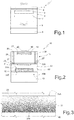
- FIG. 1 An example of a transducer element of this type is shown in Figure 1 .
- the transducer element of Figure 1 designated as a whole by reference number 1, comprises a membrane 2, for example, of silicon nitride, suspended over a cavity 3 and formed in or on a silicon chip 4.
- the cavity 3 may contain air or gas or be partially or totally in vacuum conditions.
- a conductive material layer for example of aluminium, is generally formed on the membrane 2 and forms a first electrode 6.
- Another conductive material layer forms a second electrode 10, within the chip 4, underneath the cavity 3.
- the acoustic transducer element 1 is coupled to a semiconductor material chip integrating an electronic circuit, for example, an ASIC (Application Specific Integrated Circuit) 8, for processing signals generated by or sent to the acoustic transducer element 1.
- the ASIC 8 is fixed on the back of the acoustic transducer element 1.
- the first and second electrodes 6, 7 form a capacitor that undergoes a capacitance variation when an acoustic wave hits membrane 2, causing it to deflect. This capacitance variation between the two electrodes 6, 7 may be detected by the electronic circuit, represented integrated in the ASIC 8, thus transducing the acoustic signal into an electrical signal.
- the transducer element 1 may operate both as sensor of acoustic waves and as emitter of acoustic waves.
- acoustic transducer elements In practical applications, due to the small size of the acoustic transducer elements, of the order of microns, they are generally formed close to one another, so as to form an acoustic device of sizes suited to the envisaged application.
- the acoustic transducer element 1 When the acoustic transducer element 1 operates as generator of acoustic waves, it generates the acoustic waves mainly towards the outside world. However, a part of the acoustic energy is propagated back towards the ASIC 8. This acoustic energy may be reflected towards the transducer element 1 because of the interface between the latter and the ASIC 8. To prevent such a back reflection, which could cause undesired interference phenomena with the acoustic signal, it has already been proposed to arrange an attenuating layer 9 between the chip 4 and the ASIC 8 (see, for example, U.S. patents N. 6,831,394 and 7,280,435 ).
- the attenuating layer 9 may for example be formed by a plastic material, such as an epoxy resin, polyvinyl chloride, or Teflon, containing filler material such as silver, tungsten, BN, AlN, or Al 2 O 3 .
- a plastic material such as an epoxy resin, polyvinyl chloride, or Teflon, containing filler material such as silver, tungsten, BN, AlN, or Al 2 O 3 .
- the aim of the present invention is to provide a transducer device that solves the problems encountered in the prior art.
- an acoustic transducer device is provided according to the attached claims.
- the present transducer device provides an acoustic matching region arranged between the transducer element and the attenuating layer.
- the matching region is here of porous silicon and has a variable acoustic impedance throughout its thickness, matched so as to have a value close to that of the adjacent regions. In this way, the acoustic waves that propagate backwards from the membrane do not meet any discontinuity of the acoustic impedance of the traversed media, and reflection of the acoustic waves towards the membrane is reduced.
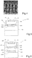
- Figure 2 shows an embodiment of an acoustic transducer device, designated as a whole by the reference number 10.
- the acoustic transducer device 10 comprises a transducer element 15 formed in a substrate 25 of semiconductor material.
- the substrate 25 has a cavity 19 that delimits, at the bottom, a membrane 16, a first electrode 20 and a second electrode 21, arranged over the membrane 16 and on the bottom of the cavity 19, respectively.
- the substrate 15, typically of mono- and/or polycrystalline silicon, may be traversed by through vias 26 of electrically conductive material.
- An ASIC 30 is bonded to the substrate 25 on the side thereof remote with respect to the membrane 16.
- the ASIC 30 has a first face 30A and a second face 30B and comprises a substrate 29 forming an active area 31 facing the first face 30A.
- the active area 31 accommodates electronic circuits (not illustrated), connected to the substrate 25 of the acoustic transducer element 15 through pads 27 and electrical connection lines (not illustrated).
- the pads 27 are in contact with the through vias 26 of the substrate 25 of the acoustic transducer element 15, inside an insulating layer 28, overlying the substrate 29.
- the ASIC 30 further forms an acoustic matching element 32, extending from the second face 30B towards the inside of the substrate 29.
- the acoustic matching element 32 is here in contact with an acoustically attenuating region 40 bonded to the second face 30B of the ASIC 8.
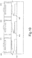
- the acoustic matching element 32 forms a first interface 32A with the substrate 29 of the ASIC 30 and a second interface 32B with the acoustically attenuating region 40, as shown in the enlarged detail of Figure 3 .
- the acoustic matching element 32 is of porous silicon and has a variable impedance between the first and second interfaces 32A, 32B.
- the impedance value of the acoustic matching element 32 in proximity of each interface 32A, 32B is chosen to correspond to the acoustic impedance of the material with which it is in contact.
- the first interface 32A has an acoustic impedance similar to that of the substrate 29 of the ASIC 30, and the second interface 32B has an acoustic impedance similar to that of the acoustically attenuating region 40.
- the impedance matching on the two interfaces 32A, 32B enables a reduction of the reflected acoustic energy.
- Z 32A is the impedance of the acoustic matching element 32 in proximity of the first interface 32A
- Z 29 is the impedance of the material of the substrate 29 (silicon)
- U T is the acoustic energy transmitted backwards by the transducer element 15.
- the reflected acoustic energy may be drastically reduced almost to zero.
- any acoustic waves that propagate back from the membrane 16 do not encounter any discontinuity in the impedance of the materials that they traverse, and therefore do not generate acoustic waves reflected towards the membrane 16, thus preventing any undesirable interference phenomena with the useful acoustic signal.
- Variation of impedance of the acoustic matching element 32 is obtained by modulating the porosity of the porous silicon.
- the porosity may be regulated by selectively modifying the size of the pores so that it is smaller in proximity of the first interface 32A and larger in proximity of the second interface 32B, varying continuously from the first interface 32A to the second interface 32B.
- the acoustic matching element 32 may, for example, be manufactured by selectively doping the substrate 29 of the ASIC 30 starting from the second face 32A with P-type dopant (for example, boron), and performing an electrochemical etch.
- P-type dopant for example, boron
- the semiconductor material wafer intended to form the ASIC 30 is implanted with the P-type dopant and then immersed in an acid bath.
- pores are formed within the doped area.
- S. Matthias, F. Müller, J. Schilling, U. Gösele "Pushing the limits of microporous silicon etching", Appl. Phys.
- a 80, 1391-1396 (2005 ), the porosity, and thus the diameter of the pores, as a function of the depth may be modulated by varying the etching parameters, in particular the applied voltage and the current flowing during the etching time so as to obtain the desired impedance values.
- the acoustic matching region 32 may also be obtained starting from a region with an N-type doping (for example, doped with phosphorus), which is rendered porous via an electrochemical etch, possibly carried out under exposure to ultraviolet and/or visible light.
- an N-type doping for example, doped with phosphorus
- the porosity, and thus the diameter of the pores may be modulated as a function of the depth by accordingly varying the etching parameters, in particular the voltage and the current flowing during the etching time.
- Figure 4 shows in detail an example of the porous silicon structure of Figure 3 .
- the acoustic matching element here designated by 132
- the substrate here designated by 125
- the impedance of the interfaces 132A and 132B is similar to that of the substrate 125 and to that of the ASIC 130, respectively.
- Figure 6 shows a further embodiment comprising a first and a second acoustic matching element 232, 233.
- the first acoustic matching element 232 is similar to the acoustic matching element 132 of Figure 5 . It is thus formed in the substrate 225 of the acoustic transducer element 215 and has, in proximity of a first interface 232A, an impedance similar to that of the substrate 225, and, in proximity of a second interface 232B, an impedance similar to that of the ASIC 230.
- the second acoustic matching element 233 is similar to the acoustic matching element 32 of Figure 2 .
- ASIC 230 It is thus formed in the ASIC 230 and has, in proximity of a first interface 233A, an impedance similar to that of the ASIC 230, and, in proximity of a second interface 233B, an impedance similar to that of the acoustically attenuating region 240.
- the acoustic matching element here designated by 332 is formed as a separate chip, arranged between the ASIC 330 and the acoustically attenuating region 340. Also in this case, the impedance of the faces 332A and 332B is similar to that of the ASIC 330 and to that of the acoustically attenuating region 340, respectively.
- the acoustic matching element here designated by 432, is formed as a separate chip, arranged between the substrate 425 of the acoustic transducer element 415 and the ASIC 430. Also in this case, the impedance of the faces 432A and 432B is similar to that of the substrate 425 and to that of the ASIC 430, respectively.
- Figure 9 shows a variation of the embodiment of Figure 6 , wherein the first and second acoustic matching elements, here designated by 532, 533, are both formed in separate dice.
- the acoustic matching element or elements 32, 132, 232, 332, 432, 532, 233, 533 reduce generation of undesired reflected waves by eliminating any sharp variations of impedance.
- the described solutions further have the advantage that the use of porous silicon enables considerable freedom of design, in particular as regards the reduction of parasitic capacitances between the ASIC 30, 130, 230, 330, 430, 530 and the substrate 25, 125, 225, 325, 425, 525.
- the described acoustic transducer device 10, 110, 210, 310, 410, 510 above may comprise a plurality of transducer elements having the structures illustrated in Figures 2-9 and formed in a single substrate.
- Figure 10 shows a substrate 625 housing a plurality of transducer elements 615, each whereof arranged on a respective active area 631 and a respective acoustic matching region 632.
- the acoustic transducer device of Figure 10 may form, for example, an ultrasonic transducer (either of a capacitive type, referred to as CMUT, and of a piezoelectric type, referred to as PMUT) for medical use, operating at frequencies comprised between 1 and 15 MHz. It may, however, be used for consumer applications wherein a high degree of miniaturization is desired, such as in gesture recognition mobile devices. Further, it may also be used for high-voltage devices and optical devices.
- CMUT capacitive type
- PMUT piezoelectric type
- the acoustically attenuating region 40 could be arranged between the transducer element 15 and the ASIC 8.
- the acoustic matching element may be arranged between the transducer element 15 and the acoustically attenuating region 40.
Landscapes
- Engineering & Computer Science (AREA)
- Mechanical Engineering (AREA)
- Physics & Mathematics (AREA)
- Acoustics & Sound (AREA)
- Multimedia (AREA)
- Signal Processing (AREA)
- Transducers For Ultrasonic Waves (AREA)
Abstract
The acoustic device has a micromachined acoustic transducer element (15); an acoustically attenuating region (40); and an acoustic matching region (32) arranged between the acoustic transducer element (15) and the acoustically attenuating region (40). The acoustic transducer element (15) is formed in a first substrate (25) housing a cavity (19) delimiting a membrane (16). A second substrate (30) of semiconductor material integrating an electronic circuit is arranged between the acoustic transducer element (15) and the acoustically attenuating region (40). The acoustic matching region (32) has a first interface (32A) with the second substrate (30) and a second interface (32B) with the acoustically attenuating region (40). The acoustic matching region (32) has an impedance matched to the impedance of the second substrate (30) in proximity of the first interface (32A), and an impedance matched to the acoustically attenuating region (40) in proximity of the second interface (32B).
Description
- The present invention relates to an integrated acoustic transducer with reduced propagation of undesired acoustic waves.
- Integrated acoustic transducers made using the semiconductor technology are known, and operate according to a capacitive principle. In some applications, these transducers are used for transducing ultrasonic waves; in this case, they are known as MUTs (Micromachined Ultrasonic Transducers), whether of a capacitive type (CMUTs - Capacitive Micromachined Ultrasonic Transducers) or of a piezoelectric type (PMUTs - Piezoelectric Micromachined Ultrasonic Transducers). For instance, CMUTs are used in ultrasound image generation systems for medical diagnostics.
- An example of a transducer element of this type is shown in
Figure 1 . - The transducer element of
Figure 1 , designated as a whole byreference number 1, comprises amembrane 2, for example, of silicon nitride, suspended over acavity 3 and formed in or on asilicon chip 4. Thecavity 3 may contain air or gas or be partially or totally in vacuum conditions. A conductive material layer, for example of aluminium, is generally formed on themembrane 2 and forms a first electrode 6. Another conductive material layer forms asecond electrode 10, within thechip 4, underneath thecavity 3. - Generally, the
acoustic transducer element 1 is coupled to a semiconductor material chip integrating an electronic circuit, for example, an ASIC (Application Specific Integrated Circuit) 8, for processing signals generated by or sent to theacoustic transducer element 1. In the embodiment illustrated, the ASIC 8 is fixed on the back of theacoustic transducer element 1. In thetransducer element 1 ofFigure 1 , the first andsecond electrodes 6, 7 form a capacitor that undergoes a capacitance variation when an acoustic wave hitsmembrane 2, causing it to deflect. This capacitance variation between the twoelectrodes 6, 7 may be detected by the electronic circuit, represented integrated in theASIC 8, thus transducing the acoustic signal into an electrical signal. Likewise, when an a.c. electrical signal is applied to one or both theelectrodes 6, 7, it causes a movement of themembrane 2 that consequently generates an acoustic signal. For this reason, thetransducer element 1 may operate both as sensor of acoustic waves and as emitter of acoustic waves. - In practical applications, due to the small size of the acoustic transducer elements, of the order of microns, they are generally formed close to one another, so as to form an acoustic device of sizes suited to the envisaged application.
- When the
acoustic transducer element 1 operates as generator of acoustic waves, it generates the acoustic waves mainly towards the outside world. However, a part of the acoustic energy is propagated back towards theASIC 8. This acoustic energy may be reflected towards thetransducer element 1 because of the interface between the latter and theASIC 8. To prevent such a back reflection, which could cause undesired interference phenomena with the acoustic signal, it has already been proposed to arrange anattenuating layer 9 between thechip 4 and the ASIC 8 (see, for example,U.S. patents N. 6,831,394 and7,280,435 ). - The
attenuating layer 9 may for example be formed by a plastic material, such as an epoxy resin, polyvinyl chloride, or Teflon, containing filler material such as silver, tungsten, BN, AlN, or Al2O3. - The known solutions do not, however, ensure a sufficient reduction of reflection because of the presence of the existing interfaces.
- The aim of the present invention is to provide a transducer device that solves the problems encountered in the prior art.
- According to the invention, an acoustic transducer device is provided according to the attached claims.
- In practice, the present transducer device provides an acoustic matching region arranged between the transducer element and the attenuating layer. The matching region is here of porous silicon and has a variable acoustic impedance throughout its thickness, matched so as to have a value close to that of the adjacent regions. In this way, the acoustic waves that propagate backwards from the membrane do not meet any discontinuity of the acoustic impedance of the traversed media, and reflection of the acoustic waves towards the membrane is reduced.
- For a better understanding of the present invention, preferred embodiments thereof are now described purely by way of non-limiting example, with reference to the attached drawings, wherein:
-
Figure 1 is a cross-section through a known acoustic transducer element; -
Figure 2 is a cross-section through the present acoustic transducer element; -
Figure 3 shows an enlarged detail of the acoustic transducer element ofFigure 2 ; -
Figure 4 shows an enlarged portion of the detail ofFigure 3 ; -
Figures 5-9 are cross-sections of different embodiments of the present acoustic transducer element; and -
Figure 10 is a cross-section of a device having a plurality of transducer elements shown inFigures 2-9 and formed in a single substrate so as to form an array. -
Figure 2 shows an embodiment of an acoustic transducer device, designated as a whole by thereference number 10. - The
acoustic transducer device 10 comprises atransducer element 15 formed in asubstrate 25 of semiconductor material. Thesubstrate 25 has acavity 19 that delimits, at the bottom, amembrane 16, afirst electrode 20 and asecond electrode 21, arranged over themembrane 16 and on the bottom of thecavity 19, respectively. Thesubstrate 15, typically of mono- and/or polycrystalline silicon, may be traversed by throughvias 26 of electrically conductive material. - An
ASIC 30 is bonded to thesubstrate 25 on the side thereof remote with respect to themembrane 16. The ASIC 30 has afirst face 30A and asecond face 30B and comprises asubstrate 29 forming anactive area 31 facing thefirst face 30A. Theactive area 31 accommodates electronic circuits (not illustrated), connected to thesubstrate 25 of theacoustic transducer element 15 throughpads 27 and electrical connection lines (not illustrated). Thepads 27 are in contact with thethrough vias 26 of thesubstrate 25 of theacoustic transducer element 15, inside aninsulating layer 28, overlying thesubstrate 29. - In
Figure 2 , the ASIC 30 further forms anacoustic matching element 32, extending from thesecond face 30B towards the inside of thesubstrate 29. The acoustic matchingelement 32 is here in contact with an acousticallyattenuating region 40 bonded to thesecond face 30B of the ASIC 8. - The
acoustic matching element 32 forms afirst interface 32A with thesubstrate 29 of theASIC 30 and asecond interface 32B with the acousticallyattenuating region 40, as shown in the enlarged detail ofFigure 3 . - The
acoustic matching element 32 is of porous silicon and has a variable impedance between the first andsecond interfaces acoustic matching element 32 in proximity of eachinterface first interface 32A has an acoustic impedance similar to that of thesubstrate 29 of theASIC 30, and thesecond interface 32B has an acoustic impedance similar to that of the acousticallyattenuating region 40. - The impedance matching on the two
interfaces interface 32A is given by:
element 32 in proximity of thefirst interface 32A, Z29 is the impedance of the material of the substrate 29 (silicon), and UT is the acoustic energy transmitted backwards by thetransducer element 15. - By modulating the impedance Z32A of the acoustic matching
element 32 in proximity of thefirst interface 32A so that it is approximately equal to the impedance Z29 of thesilicon substrate 29, Z32A ≈ Z29, the reflected acoustic energy may be drastically reduced almost to zero. - Likewise, the acoustic energy reflected on the
interface 32B is given by:
acoustic matching element 32 in proximity of thesecond interface 32B, Z40 is the impedance of the material of the acoustically attenuatingregion 40, and UT1 is the acoustic energy traversing thesecond interface 32B. - Also in this case, by modulating the impedance Z32B of the
acoustic matching element 32 in proximity of thesecond interface 32B so that it is approximately equal to the impedance Z40 of the acousticallyattenuating region 40, Z32A ≈ Z40, the acoustic energy reflected on thesecond interface 32B is reduced. - In practice, any acoustic waves that propagate back from the
membrane 16 do not encounter any discontinuity in the impedance of the materials that they traverse, and therefore do not generate acoustic waves reflected towards themembrane 16, thus preventing any undesirable interference phenomena with the useful acoustic signal. - Variation of impedance of the acoustic matching
element 32 is obtained by modulating the porosity of the porous silicon. In particular, the porosity may be regulated by selectively modifying the size of the pores so that it is smaller in proximity of thefirst interface 32A and larger in proximity of thesecond interface 32B, varying continuously from thefirst interface 32A to thesecond interface 32B. - The
acoustic matching element 32 may, for example, be manufactured by selectively doping thesubstrate 29 of the ASIC 30 starting from thesecond face 32A with P-type dopant (for example, boron), and performing an electrochemical etch. In particular, before forming the electrical components in theactive part 31, the semiconductor material wafer intended to form theASIC 30 is implanted with the P-type dopant and then immersed in an acid bath. By applying an appropriate potential difference and modulating the current flowing in the wafer with time, pores are formed within the doped area. In particular, as explained in the article by S. Matthias, F. Müller, J. Schilling, U. Gösele, "Pushing the limits of microporous silicon etching", Appl. Phys. A 80, 1391-1396 (2005), the porosity, and thus the diameter of the pores, as a function of the depth may be modulated by varying the etching parameters, in particular the applied voltage and the current flowing during the etching time so as to obtain the desired impedance values. - The
acoustic matching region 32 may also be obtained starting from a region with an N-type doping (for example, doped with phosphorus), which is rendered porous via an electrochemical etch, possibly carried out under exposure to ultraviolet and/or visible light. Also in this case, the porosity, and thus the diameter of the pores, may be modulated as a function of the depth by accordingly varying the etching parameters, in particular the voltage and the current flowing during the etching time. -
Figure 4 shows in detail an example of the porous silicon structure ofFigure 3 . - In another embodiment, shown in
Figure 5 , the acoustic matching element, here designated by 132, is formed within the substrate, here designated by 125, instead of inside theASIC 130. In this case, the impedance of theinterfaces substrate 125 and to that of theASIC 130, respectively. -
Figure 6 shows a further embodiment comprising a first and a secondacoustic matching element acoustic matching element 232 is similar to theacoustic matching element 132 ofFigure 5 . It is thus formed in thesubstrate 225 of theacoustic transducer element 215 and has, in proximity of afirst interface 232A, an impedance similar to that of thesubstrate 225, and, in proximity of asecond interface 232B, an impedance similar to that of theASIC 230. The secondacoustic matching element 233 is similar to theacoustic matching element 32 ofFigure 2 . It is thus formed in theASIC 230 and has, in proximity of afirst interface 233A, an impedance similar to that of theASIC 230, and, in proximity of asecond interface 233B, an impedance similar to that of theacoustically attenuating region 240. - In this way, there is a double acoustic matching both between the
substrate 225 and theASIC 230 and between theASIC 230 and the acoustically attenuatingregion 240. - In another embodiment, shown in
Figure 7 , the acoustic matching element, here designated by 332, is formed as a separate chip, arranged between theASIC 330 and the acoustically attenuatingregion 340. Also in this case, the impedance of the faces 332A and 332B is similar to that of theASIC 330 and to that of theacoustically attenuating region 340, respectively. - In another embodiment, shown in
Figure 8 , the acoustic matching element, here designated by 432, is formed as a separate chip, arranged between thesubstrate 425 of theacoustic transducer element 415 and theASIC 430. Also in this case, the impedance of thefaces substrate 425 and to that of theASIC 430, respectively. -
Figure 9 shows a variation of the embodiment ofFigure 6 , wherein the first and second acoustic matching elements, here designated by 532, 533, are both formed in separate dice. - In all the illustrated embodiments, the acoustic matching element or
elements - The described solutions further have the advantage that the use of porous silicon enables considerable freedom of design, in particular as regards the reduction of parasitic capacitances between the
ASIC substrate - The described
acoustic transducer device Figures 2-9 and formed in a single substrate. For instance,Figure 10 shows asubstrate 625 housing a plurality oftransducer elements 615, each whereof arranged on a respectiveactive area 631 and a respectiveacoustic matching region 632. - The acoustic transducer device of
Figure 10 may form, for example, an ultrasonic transducer (either of a capacitive type, referred to as CMUT, and of a piezoelectric type, referred to as PMUT) for medical use, operating at frequencies comprised between 1 and 15 MHz. It may, however, be used for consumer applications wherein a high degree of miniaturization is desired, such as in gesture recognition mobile devices. Further, it may also be used for high-voltage devices and optical devices. - Finally, it is clear that modifications and variations may be made to the device described and illustrated herein, without thereby departing from the scope of the present invention, as defined in the attached claims.
- For instance, the acoustically attenuating
region 40 could be arranged between thetransducer element 15 and theASIC 8. In this case, the acoustic matching element may be arranged between thetransducer element 15 and the acoustically attenuatingregion 40.
Claims (17)
- An acoustic device comprising:a micromachined acoustic transducer element (15; 115; 215; 315; 415; 515);an acoustically attenuating region (40; 140; 240; 340; 340; 440; 540); andan acoustic matching region (32; 132; 232; 432; 532; 233; 533) arranged between the acoustic transducer element (15; 115; 215; 315; 415; 515) and the acoustically attenuating region (40; 140; 240; 340; 340; 440; 540).
- A device according to claim 1, wherein the acoustic transducer element (15; 115; 215; 315; 415; 515) is formed in a first substrate (25, 125; 225; 325; 325; 425; 525) housing a cavity (19) delimiting a membrane (16).
- A device according to claim 2, further comprising a second substrate (30; 130; 230; 230, 330; 430; 530) of semiconductor material integrating an electronic circuit and arranged between the acoustic transducer element (15; 115; 215; 315; 415; 515) and the acoustically attenuating region (40; 140; 240; 340; 340; 440; 540).
- A device according to claim 3, wherein the acoustic matching region (132; 232; 432; 532) is arranged between the acoustic transducer element (115; 215; 415; 515) and the second substrate (130; 230; 430; 530).
- A device according to claim 4, wherein the acoustic matching region (132; 232) is formed in the first substrate (125, 225) of the acoustic transducer element (115; 215).
- A device according to claim 4, wherein the acoustic matching region (432; 532) is formed in a semiconductor material body arranged between the first substrate (425; 525) and the second substrate (430; 530).
- A device according to claim 5 or 6, wherein the acoustic matching region (232; 532) is a first acoustic matching region, the device further comprising a second acoustic matching region (233; 533) arranged between the second substrate (30) and the acoustically attenuating region (240; 540).
- A device according to claim 7, wherein the second acoustic matching region (233) is formed in the second substrate (230).
- A device according to claim 4, wherein the acoustic matching region (32; 233; 332; 532) is arranged between the second substrate (30; 230; 330; 530) and the acoustically attenuating region (40; 240; 340; 540).
- A device according to claim 9, wherein the acoustic matching region (32; 233) is formed in the second substrate (30; 230).
- A device according to claim 9, wherein the acoustic matching region (332; 533) is formed in a semiconductor material body arranged between the second substrate (330; 530) and the acoustically attenuating region (340; 540).
- A device according to claim 10, wherein the second acoustic matching region (533) is formed in a semiconductor material body arranged between the second substrate (530) and the acoustically attenuating region (540).
- A device according to any of claims 3-12, wherein the first acoustic matching element (32; 132; 232; 432; 532; 233; 533) comprises a variable impedance layer.
- A device according to claim 13, wherein the acoustic matching region (32; 132; 232; 432; 532; 233; 533) has a first interface (32A; 132A; 232A; 432A; 532A; 233A; 533A) with a first element chosen between the acoustic transducer element (15; 115; 215; 315; 415; 515) and the second substrate (30; 130; 230; 230, 330; 430; 530) and a second interface (32B; 132B; 232B; 432B; 532B; 233B; 533B) with a second element chosen between the second substrate (30; 130; 230; 230, 330; 430; 530) and the acoustically attenuating region (40; 140; 240; 340; 340; 440; 540), the first element having a first impedance and the second element having a second impedance, and the acoustic matching region (32; 132; 232; 432; 532; 233; 533) has a third impedance in proximity of the first interface, matched to the first impedance, and a fourth impedance in proximity of the second interface, matched to the second impedance.
- A device according to any of claims 1-14, wherein the acoustic matching region (32; 132; 232; 432; 532; 233; 533) is of porous silicon.
- A device according to claim 15 when depending on claim 14, wherein the acoustic matching region (32; 132; 232; 432; 532; 233; 533) has a plurality of pores, wherein the sizes of the pores are variable between the first and second interfaces (32A; 132A; 232A; 432A; 532A; 233A; 533A, 32B; 132B; 232B; 432B; 532B; 233B; 533B).
- A device according to any of the preceding claims, forming an ultrasonic transducer (CMUT; PMUT) for medical use.
Applications Claiming Priority (1)
| Application Number | Priority Date | Filing Date | Title |
|---|---|---|---|
| ITUA2016A003033A ITUA20163033A1 (en) | 2016-04-29 | 2016-04-29 | INTEGRATED ACOUSTIC TRANSDUCER WITH REDUCED PROPAGATION OF UNWANTED ACOUSTIC WAVES |
Publications (1)
| Publication Number | Publication Date |
|---|---|
| EP3238629A1 true EP3238629A1 (en) | 2017-11-01 |
Family
ID=56682211
Family Applications (1)
| Application Number | Title | Priority Date | Filing Date |
|---|---|---|---|
| EP16206869.6A Withdrawn EP3238629A1 (en) | 2016-04-29 | 2016-12-23 | Integrated acoustic transducer with reduced propagation of undesired acoustic waves |
Country Status (4)
| Country | Link |
|---|---|
| US (1) | US20170312782A1 (en) |
| EP (1) | EP3238629A1 (en) |
| CN (2) | CN107343246A (en) |
| IT (1) | ITUA20163033A1 (en) |
Cited By (1)
| Publication number | Priority date | Publication date | Assignee | Title |
|---|---|---|---|---|
| CN114101015A (en) * | 2022-01-25 | 2022-03-01 | 深圳市大族光电设备有限公司 | Ultrasonic transducer and control system, method and device thereof |
Families Citing this family (6)
| Publication number | Priority date | Publication date | Assignee | Title |
|---|---|---|---|---|
| ITUA20163033A1 (en) * | 2016-04-29 | 2017-10-29 | St Microelectronics Srl | INTEGRATED ACOUSTIC TRANSDUCER WITH REDUCED PROPAGATION OF UNWANTED ACOUSTIC WAVES |
| WO2021014222A2 (en) * | 2019-07-24 | 2021-01-28 | Vermon Sa | Panel transducer scale package and method of manufacturing the same |
| EP4645300A3 (en) | 2020-03-05 | 2026-01-28 | Exo Imaging Inc. | Ultrasonic imaging device with programmable anatomy and flow imaging |
| US20220304659A1 (en) * | 2021-03-29 | 2022-09-29 | Exo Imaging, Inc. | Trenches for the reduction of cross-talk in mut arrays |
| US12486159B2 (en) | 2021-06-30 | 2025-12-02 | Exo Imaging, Inc. | Micro-machined ultrasound transducers with insulation layer and methods of manufacture |
| DE102021213327B3 (en) | 2021-11-26 | 2023-03-16 | Carl Zeiss Smt Gmbh | Metrology system for examining objects with EUV measuring light |
Citations (4)
| Publication number | Priority date | Publication date | Assignee | Title |
|---|---|---|---|---|
| US6831394B2 (en) | 2002-12-11 | 2004-12-14 | General Electric Company | Backing material for micromachined ultrasonic transducer devices |
| US20070164632A1 (en) * | 2004-03-06 | 2007-07-19 | Olympus Corporation | Capacitive ultrasonic transducer, production method thereof, and capacitive ultrasonic probe |
| US7280435B2 (en) | 2003-03-06 | 2007-10-09 | General Electric Company | Switching circuitry for reconfigurable arrays of sensor elements |
| US9154057B2 (en) * | 2010-06-07 | 2015-10-06 | Canon Kabushiki Kaisha | Electromechanical transducer device and analyte information acquiring apparatus |
Family Cites Families (7)
| Publication number | Priority date | Publication date | Assignee | Title |
|---|---|---|---|---|
| US6639339B1 (en) * | 2000-05-11 | 2003-10-28 | The Charles Stark Draper Laboratory, Inc. | Capacitive ultrasound transducer |
| WO2004102203A1 (en) * | 2003-05-16 | 2004-11-25 | Olympus Corporation | Ultrasonic platform-type microchip and method for driving ultrasonic transducer array |
| US7880565B2 (en) * | 2005-08-03 | 2011-02-01 | Kolo Technologies, Inc. | Micro-electro-mechanical transducer having a surface plate |
| US8316518B2 (en) * | 2008-09-18 | 2012-11-27 | Visualsonics Inc. | Methods for manufacturing ultrasound transducers and other components |
| JP6149425B2 (en) * | 2013-03-01 | 2017-06-21 | コニカミノルタ株式会社 | Manufacturing method of ultrasonic probe |
| JP6402983B2 (en) * | 2014-08-29 | 2018-10-10 | セイコーエプソン株式会社 | Ultrasonic device, method for manufacturing ultrasonic device, ultrasonic probe, ultrasonic measuring device, electronic equipment |
| ITUA20163033A1 (en) * | 2016-04-29 | 2017-10-29 | St Microelectronics Srl | INTEGRATED ACOUSTIC TRANSDUCER WITH REDUCED PROPAGATION OF UNWANTED ACOUSTIC WAVES |
-
2016
- 2016-04-29 IT ITUA2016A003033A patent/ITUA20163033A1/en unknown
- 2016-12-23 EP EP16206869.6A patent/EP3238629A1/en not_active Withdrawn
- 2016-12-29 CN CN201611248216.5A patent/CN107343246A/en active Pending
- 2016-12-29 CN CN201621467767.6U patent/CN206993400U/en not_active Expired - Fee Related
-
2017
- 2017-03-20 US US15/463,858 patent/US20170312782A1/en not_active Abandoned
Patent Citations (4)
| Publication number | Priority date | Publication date | Assignee | Title |
|---|---|---|---|---|
| US6831394B2 (en) | 2002-12-11 | 2004-12-14 | General Electric Company | Backing material for micromachined ultrasonic transducer devices |
| US7280435B2 (en) | 2003-03-06 | 2007-10-09 | General Electric Company | Switching circuitry for reconfigurable arrays of sensor elements |
| US20070164632A1 (en) * | 2004-03-06 | 2007-07-19 | Olympus Corporation | Capacitive ultrasonic transducer, production method thereof, and capacitive ultrasonic probe |
| US9154057B2 (en) * | 2010-06-07 | 2015-10-06 | Canon Kabushiki Kaisha | Electromechanical transducer device and analyte information acquiring apparatus |
Non-Patent Citations (1)
| Title |
|---|
| S. MATTHIAS; F. MULLER; J. SCHILLING; U. GOSELE: "Pushing the limits of microporous silicon etching", APPL. PHYS. A, vol. 80, 2005, pages 1391 - 1396, XP019336751, DOI: doi:10.1007/s00339-004-3193-x |
Cited By (1)
| Publication number | Priority date | Publication date | Assignee | Title |
|---|---|---|---|---|
| CN114101015A (en) * | 2022-01-25 | 2022-03-01 | 深圳市大族光电设备有限公司 | Ultrasonic transducer and control system, method and device thereof |
Also Published As
| Publication number | Publication date |
|---|---|
| CN107343246A (en) | 2017-11-10 |
| ITUA20163033A1 (en) | 2017-10-29 |
| CN206993400U (en) | 2018-02-09 |
| US20170312782A1 (en) | 2017-11-02 |
Similar Documents
| Publication | Publication Date | Title |
|---|---|---|
| US10322929B2 (en) | Monolithic integration of PMUT on CMOS | |
| US20170312782A1 (en) | Integrated acoustic transducer with reduced propagation of undesired acoustic waves | |
| JP5009301B2 (en) | Ultrasonic probe and ultrasonic diagnostic apparatus using the same | |
| CN105828962B (en) | Monolithically integrated three-electrode CMUT device | |
| US8540640B2 (en) | Ultrasonic probe and method for manufacturing the same and ultrasonic diagnostic device | |
| EP1992421B1 (en) | Semiconductor device | |
| EP2213239A1 (en) | Ultrasonic imaging device | |
| JP4624763B2 (en) | Capacitive ultrasonic transducer and manufacturing method thereof | |
| US6714484B2 (en) | Microfabricated acoustic transducer with suppressed substrate modes | |
| CN1283547C (en) | Micro-machined ultrasonic transducer (MUT) substrate that limits the lateral propagation of acoustic energy | |
| EP4247567B1 (en) | An ultrasonic transducer structure | |
| CN106536068A (en) | Ultrasound transducer arrangement and assembly, coaxial wire assembly, ultrasound probe and ultrasonic imaging system | |
| KR101761819B1 (en) | Ultrasonic transducer and method of manufacturing the sames | |
| CN108136440A (en) | IC dies, probes and ultrasound systems | |
| JP2008099036A (en) | Ultrasonic transducer, ultrasonic probe and ultrasonic diagnostic apparatus | |
| CN102770078A (en) | Ultrasonic probe and ultrasonic image pickup device using same | |
| KR102184454B1 (en) | Ultrasonic transducer and method of manufacturing ultrasonic transducer | |
| JP4839176B2 (en) | Ultrasonic transducer and ultrasonic diagnostic apparatus | |
| Dausch et al. | 5I-4 Piezoelectric micromachined ultrasound transducer (pMUT) arrays for 3D imaging probes | |
| CN107921477B (en) | Capacitive micromachined ultrasonic transducer with improved patient safety | |
| JP6942670B2 (en) | Ultrasound inspection equipment and ultrasonic probe | |
| JP2018140061A (en) | Ultrasonic imaging apparatus | |
| JP5026770B2 (en) | Ultrasonic probe and ultrasonic diagnostic apparatus | |
| US20150229236A1 (en) | Zero-bias capacitive micromachined ultrasonic transducers and fabrication method thereof | |
| US12486159B2 (en) | Micro-machined ultrasound transducers with insulation layer and methods of manufacture |
Legal Events
| Date | Code | Title | Description |
|---|---|---|---|
| PUAI | Public reference made under article 153(3) epc to a published international application that has entered the european phase |
Free format text: ORIGINAL CODE: 0009012 |
|
| AK | Designated contracting states |
Kind code of ref document: A1 Designated state(s): AL AT BE BG CH CY CZ DE DK EE ES FI FR GB GR HR HU IE IS IT LI LT LU LV MC MK MT NL NO PL PT RO RS SE SI SK SM TR |
|
| AX | Request for extension of the european patent |
Extension state: BA ME |
|
| STAA | Information on the status of an ep patent application or granted ep patent |
Free format text: STATUS: THE APPLICATION IS DEEMED TO BE WITHDRAWN |
|
| 18D | Application deemed to be withdrawn |
Effective date: 20180503 |