EP3238610A1 - Flexible extensile electronic device based on biocompatible film and preparation method - Google Patents
Flexible extensile electronic device based on biocompatible film and preparation method Download PDFInfo
- Publication number
- EP3238610A1 EP3238610A1 EP15871847.8A EP15871847A EP3238610A1 EP 3238610 A1 EP3238610 A1 EP 3238610A1 EP 15871847 A EP15871847 A EP 15871847A EP 3238610 A1 EP3238610 A1 EP 3238610A1
- Authority
- EP
- European Patent Office
- Prior art keywords
- layer
- biocompatible
- flexible
- functional
- electronic device
- Prior art date
- Legal status (The legal status is an assumption and is not a legal conclusion. Google has not performed a legal analysis and makes no representation as to the accuracy of the status listed.)
- Granted
Links
Images

Classifications
-
- A—HUMAN NECESSITIES
- A61—MEDICAL OR VETERINARY SCIENCE; HYGIENE
- A61B—DIAGNOSIS; SURGERY; IDENTIFICATION
- A61B5/00—Measuring for diagnostic purposes; Identification of persons
-
- A—HUMAN NECESSITIES
- A61—MEDICAL OR VETERINARY SCIENCE; HYGIENE
- A61B—DIAGNOSIS; SURGERY; IDENTIFICATION
- A61B5/00—Measuring for diagnostic purposes; Identification of persons
- A61B5/68—Arrangements of detecting, measuring or recording means, e.g. sensors, in relation to patient
- A61B5/6801—Arrangements of detecting, measuring or recording means, e.g. sensors, in relation to patient specially adapted to be attached to or worn on the body surface
- A61B5/683—Means for maintaining contact with the body
- A61B5/6832—Means for maintaining contact with the body using adhesives
- A61B5/6833—Adhesive patches
-
- A—HUMAN NECESSITIES
- A61—MEDICAL OR VETERINARY SCIENCE; HYGIENE
- A61B—DIAGNOSIS; SURGERY; IDENTIFICATION
- A61B5/00—Measuring for diagnostic purposes; Identification of persons
- A61B5/0002—Remote monitoring of patients using telemetry, e.g. transmission of vital signals via a communication network
- A61B5/0015—Remote monitoring of patients using telemetry, e.g. transmission of vital signals via a communication network characterised by features of the telemetry system
- A61B5/0024—Remote monitoring of patients using telemetry, e.g. transmission of vital signals via a communication network characterised by features of the telemetry system for multiple sensor units attached to the patient, e.g. using a body or personal area network
-
- A—HUMAN NECESSITIES
- A61—MEDICAL OR VETERINARY SCIENCE; HYGIENE
- A61B—DIAGNOSIS; SURGERY; IDENTIFICATION
- A61B5/00—Measuring for diagnostic purposes; Identification of persons
- A61B5/01—Measuring temperature of body parts ; Diagnostic temperature sensing, e.g. for malignant or inflamed tissue
-
- A—HUMAN NECESSITIES
- A61—MEDICAL OR VETERINARY SCIENCE; HYGIENE
- A61B—DIAGNOSIS; SURGERY; IDENTIFICATION
- A61B5/00—Measuring for diagnostic purposes; Identification of persons
- A61B5/02—Detecting, measuring or recording for evaluating the cardiovascular system, e.g. pulse, heart rate, blood pressure or blood flow
- A61B5/024—Measuring pulse rate or heart rate
- A61B5/02416—Measuring pulse rate or heart rate using photoplethysmograph signals, e.g. generated by infrared radiation
- A61B5/02427—Details of sensor
-
- H—ELECTRICITY
- H05—ELECTRIC TECHNIQUES NOT OTHERWISE PROVIDED FOR
- H05K—PRINTED CIRCUITS; CASINGS OR CONSTRUCTIONAL DETAILS OF ELECTRIC APPARATUS; MANUFACTURE OF ASSEMBLAGES OF ELECTRICAL COMPONENTS
- H05K1/00—Printed circuits
- H05K1/02—Details
- H05K1/0277—Bendability or stretchability details
- H05K1/0283—Stretchable printed circuits
-
- H—ELECTRICITY
- H05—ELECTRIC TECHNIQUES NOT OTHERWISE PROVIDED FOR
- H05K—PRINTED CIRCUITS; CASINGS OR CONSTRUCTIONAL DETAILS OF ELECTRIC APPARATUS; MANUFACTURE OF ASSEMBLAGES OF ELECTRICAL COMPONENTS
- H05K1/00—Printed circuits
- H05K1/02—Details
- H05K1/11—Printed elements for providing electric connections to or between printed circuits
- H05K1/118—Printed elements for providing electric connections to or between printed circuits specially for flexible printed circuits, e.g. using folded portions
-
- A—HUMAN NECESSITIES
- A61—MEDICAL OR VETERINARY SCIENCE; HYGIENE
- A61B—DIAGNOSIS; SURGERY; IDENTIFICATION
- A61B2562/00—Details of sensors; Constructional details of sensor housings or probes; Accessories for sensors
- A61B2562/12—Manufacturing methods specially adapted for producing sensors for in-vivo measurements
-
- H—ELECTRICITY
- H05—ELECTRIC TECHNIQUES NOT OTHERWISE PROVIDED FOR
- H05K—PRINTED CIRCUITS; CASINGS OR CONSTRUCTIONAL DETAILS OF ELECTRIC APPARATUS; MANUFACTURE OF ASSEMBLAGES OF ELECTRICAL COMPONENTS
- H05K2201/00—Indexing scheme relating to printed circuits covered by H05K1/00
- H05K2201/01—Dielectrics
- H05K2201/0104—Properties and characteristics in general
- H05K2201/0116—Porous, e.g. foam
-
- H—ELECTRICITY
- H05—ELECTRIC TECHNIQUES NOT OTHERWISE PROVIDED FOR
- H05K—PRINTED CIRCUITS; CASINGS OR CONSTRUCTIONAL DETAILS OF ELECTRIC APPARATUS; MANUFACTURE OF ASSEMBLAGES OF ELECTRICAL COMPONENTS
- H05K2201/00—Indexing scheme relating to printed circuits covered by H05K1/00
- H05K2201/01—Dielectrics
- H05K2201/0104—Properties and characteristics in general
- H05K2201/0133—Elastomeric or compliant polymer
-
- H—ELECTRICITY
- H05—ELECTRIC TECHNIQUES NOT OTHERWISE PROVIDED FOR
- H05K—PRINTED CIRCUITS; CASINGS OR CONSTRUCTIONAL DETAILS OF ELECTRIC APPARATUS; MANUFACTURE OF ASSEMBLAGES OF ELECTRICAL COMPONENTS
- H05K2201/00—Indexing scheme relating to printed circuits covered by H05K1/00
- H05K2201/09—Shape and layout
- H05K2201/09209—Shape and layout details of conductors
- H05K2201/09218—Conductive traces
- H05K2201/09263—Meander
Definitions
- the present invention relates to a flexible and stretchable electronic device based on a biocompatible film and a method for preparing the same, which is applicable but not limited to various vital sign sensors.
- the devices for testing the corresponding signals such as mercury thermometer, hand hold pulse oximeter, ECG electrode and so on, adopt a hard-to-soft contact type. They all employ reliable and effective principles of physical chemistry.
- the discomfort caused by hard contact to the patient may affect the performance of normal physiological parameters; the mismatch of hard contact will make the detection signal be affected by the contact extent; and 24-hour comfortable and effective health monitoring cannot be achieved by means of such equipments. Therefore, the research on electronic components/elements integratable with human body, as a large branch of flexible electronics, has a wide range of civil business value.
- the sensors use thin and flexible polymer film material as a substrate to enable the flexible functional devices to contact with human skin directly or indirectly by using a bonding layer or Van der Waals force, thereby acquiring a variety of physiological signals on the skin surface.
- the above researches focus on how devices can achieve flexibility and stretchability, and lack the consideration of biocompatibility of devices on human body surface over long periods.
- the flexible devices using Van der Waals force to adhere have poor adhesion to hairy skin.
- the flexible devices using a bonding layer to adhere are difficult to be kept on the skin surface of the human body for a long time due to lack of breathability.
- the flexible and stretchable electronic device based on the biocompatible film has the following properties, comprising, but not limited to, 1 biocompatibility: the device does not chemically contain chemical compositions which are harmful to the human body, and the device has air permeability physically, so that the sweat on the body surface can evaporate normally, thereby avoiding maceration or allergic reaction; and 2 flexibility and stretchability: flexibility requires that the bending stiffness of the device (comprising the substrate layer and the functional layer) is small so that the device can be flexibly bent to be adapt to the natural curvature of the surface of the human tissue, and stretchability requires that the tensile stiffness of the device is small so that the device can be deformed in the in-plane direction to be adapt to the non-developable surface of the human tissue.
- a flexible and stretchable electronic device based on a biocompatible film comprises an encapsulation layer, a functional layer and a substrate layer, wherein the encapsulation layer employs a biocompatible encapsulation layer, and the substrate layer employs a biocompatible substrate layer.
- the biocompatible encapsulation layer and the biocompatible substrate layer each employs a biocompatible film.
- the technique of the present invention is also characterized in that a bonding layer is provided between the biocompatible encapsulation layer and the functional layer, and the bonding layer is used for enhancing an interfacial strength between the biocompatible encapsulation layer and the functional layer.
- An adhesion layer is provided under the biocompatible substrate layer, and the adhesion layer is used for enhancing an adhesive force between the device and a surface of an object to be detected.
- the biocompatible film of the present invention is a polymer film or a biologic semi-permeable membrane featuring with porous microstructures.
- the thickness of the biocompatible encapsulation layer is the same as the thickness of the biocompatible substrate layer.
- the functional layer of the present invention comprises a functional element, an interconnection wire, and an extraction electrode.
- the functional element employs a material having thermo-resistive effect, piezoresistive effect, or piezoelectric effect.
- the functional layer of the present invention employs a flexible and stretchable structure.
- the flexible and stretchable structure preferably employs an island-bridge structure, an S-shaped structure or a wavy buckling structure.
- the present invention provides a method for preparing a flexible and stretchable electronic device based on a biocompatible film, wherein the method comprises the following steps:
- the functional layer is integrated with the biocompatible substrate layer by using transfer printing technique.
- the present invention Compared with the conventional flexible and stretchable electronic device, the present invention has the following advantages and high-lighting technical effects: the device fabricated using the method of the present invention employs a biocompatible encapsulation layer and a stretchable biocompatible substrate layer to introduce good biocompatibility for conventional flexible and stretchable electronic device while maintaining or even enhancing the flexibility and stretchability thereof. Meanwhile, the biocompatibility properties of the device, such as being waterproof and air permeable, hypoallergenic, etc., allow the device to work normally on the human body surface for more than 24 hours, without foreign body sensation and discomfort, and thus, skin maceration, redness or other allergic reactions due to poor biocompatibility (airtight) can be avoided.
- the biocompatibility properties of the device such as being waterproof and air permeable, hypoallergenic, etc.
- Fig. 1 and Fig. 2 show a layered three-dimensional structure and a layered schematic sectional view of a flexible and stretchable electronic device based on a biocompatible film provided by the present invention.
- the basic structure of the flexible and stretchable electronic device is the biocompatible encapsulation layer / the functional layer / the biocompatible substrate layer, wherein the biocompatible encapsulation layer 1 is a kind of film having biocompatibility, comprising but not limited to, polymer film having porous microstructure (e.g., porous polyurethane film) or biologic semi-permeable membrane (e.g., biological tissue film with selective permeability), and has a thickness of several tens of microns, and the main feature is that the non-penetrating holes having diameters ranging from hundreds of nanometers to tens of microns are distributed on the film, oxygen and water vapor can pass through the holes, but liquid water and bacteria cannot pass through the holes. Therefore, such kind of film has biocompatibility, waterproof and breathable function,
- the biocompatible substrate layer 5 is also made of a film having biocompatibility described above for supporting the functional element 3 and the interconnection wire 4.
- Each of the functional element 3 and the interconnection wire 4 is designed to have flexibility and stretchability, the non-stretchable functional element 3 may be provided with a buffer layer to isolate strain, and the stretchability of the interconnection wire 4 is achieved through an S-shaped fractal design.
- the wire with the S-shaped fractal design is adapted to the tensile deformation in the substrate surface by increasing the wavelength and reducing the amplitude in the in-plane direction.
- the biocompatible film is used as the flexible substrate layer, so as to utilize the air permeability, water resistance, and low sensitization of the biocompatible film to provide the biocompatibility for the entire device, so that the device can operate on the human tissue (comprising but not limited to, the skin) surface more than 24 hours.
- An integrated functional layer of the device is provided on the biocompatible substrate layer 5, and the functional layer comprises various functional elements 3, interconnection wires 4, and extraction electrodes.
- Each type of functional elements 3 and their interconnection wires 4 are designed to have a flexible and stretchable structure, such as an island bridge structure, a buckling structure or an in-plane bending structure.
- the biocompatible encapsulation layer 1 is used for encapsulating to protect the structural integrity of the functional device, and prevent the circuit function and biocompatibility from being destroyed by external liquid.
- the device may be integrally encapsulated, or only parts of the device where the functional elements 3 and the interconnection wires 4 exist may be locally encapsulated.
- the device is finally encapsulated with a biocompatible encapsulation layer 1 having the same thickness as the biocompatible substrate layer 5.
- a biocompatible encapsulation layer 1 having the same thickness as the biocompatible substrate layer 5.
- a bonding layer 2 is selectively provided between the biocompatible encapsulation layer 1 and the functional layer, and has a thickness of about several microns. If both the biocompatible encapsulation layer 1 and the functional layer are thin enough, the biocompatible encapsulation layer 1 and the functional layer can be bonded with each other by using Van der Waals force without the bonding layer 2.
- An adhesion layer 6 is selectively provided between the biocompatible substrate layer 5 and the surface (human skin) of the object to be detected for enhancing the adhesive force between the device and the surface of the object to be detected.
- the adhesion layer is formed by a material with strong viscosity and very low sensitization, which enables the entire device to securely contact with the human tissue surface and be less prone to debond.
- the element in the functional layer may be a temperature sensing member utilizing thermo-resistive effect of the metal, a strain sensing member utilizing piezoresistive effect of the semiconductor or metal, or an energy harvesting member utilizing piezoelectric effect of the piezoelectric material, etc.
- Different functional materials and structural forms may achieve different types of signal acquisition functions.
- the elements of the biocompatible flexible and stretchable electronic device with a single function or multiple functions may be prepared using the preparing process shown in Fig. 3 .
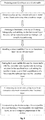
- Fig. 3 is a process flow diagram of a method for preparing a flexible and stretchable electronic device based on a biocompatible film according to the present invention, and the method comprises the following steps:
- the steps 2) to 3) may be repeated if required according to the functional design requirements on different devices, so as to prepare a plurality of layers, and insulating layers are used for isolating respective layers, or the respective layers are perforated to facilitate connection.
- the step 4) (transfer print), the biocompatible film may be bonded to the functional layer on the silicon wafer through the bonding layer 2, and then the biocompatible film and the silicon wafer may be put into the etching solution for the sacrificial layer to etch the sacrificial layer, thereby completing the process for transferring the functional layer to the flexible substrate layer.
- a transfer stamp with a novel microstructure may be used for integrating the functional layer with the flexible substrate layer without using the bonding layer 2.
- a layer of adhesion layer 6 may be used for reinforcing the bonding between the skin and the biocompatible substrate layer 5. If the thickness of the device is small enough, the adhesion layer 6 is not used, and the device and the skin are securely bonded to each other under Van der Waals force directly.
- a biocompatible film is used as the biocompatible substrate layer 5, the functional layer is prepared on the silicon wafer by using traditional semiconductor technology, film growth technique, lithography technology and the like, and a biocompatible film is used as a biocompatible encapsulation layer 1 on the top.
- Adhesive with lower sensitization which is used as the bonding layer 2 and the adhesion layer 6, is applied between the functional layer and the biocompatible encapsulation layer 1, and between the biocompatible substrate layer 5 and the surface of the object to be detected.
- the integration of the functional layer with the biocompatible substrate layer 5 may be achieved by the transfer printing method during preparation.
- the integration of the functional layer with the biocompatible substrate layer 5 is achieved by the transfer printing method.
- the functional layer is prepared on the silicon wafer using conventional semiconductor processes, comprising film growth, lithography, etching, and the like.
- a sacrificial layer is prepared in advance on the silicon wafer to facilitate stripping of the functional layer from the silicon wafer, and facilitate transfer printing.
- Requirements to be met in selection of materials and preparation processes of the sacrificial layer 1) capable of ensuring smooth completion of functional layer preparation, that is, the sacrificial layer has a flatness, hardness and glass transition temperature which meet the requirements on the film growth conditions of the functional part, and do not affect the film growth quality; 2) capable of ensuring smooth completion of patterning etching of the functional part, that is, the sacrificial layer can withstand physical and chemical reactions in the lithography process and etching process, and may not be vitrified; and 3) after the preparation of the functional layer is completed, the sacrificial layer can be easily etched, and the reaction does not affect the pattern and the material properties of the functional part.
Landscapes
- Health & Medical Sciences (AREA)
- Life Sciences & Earth Sciences (AREA)
- Engineering & Computer Science (AREA)
- Medical Informatics (AREA)
- Surgery (AREA)
- Veterinary Medicine (AREA)
- Biophysics (AREA)
- Pathology (AREA)
- Biomedical Technology (AREA)
- Heart & Thoracic Surgery (AREA)
- Public Health (AREA)
- Molecular Biology (AREA)
- Physics & Mathematics (AREA)
- Animal Behavior & Ethology (AREA)
- General Health & Medical Sciences (AREA)
- Microelectronics & Electronic Packaging (AREA)
- Cardiology (AREA)
- Computer Networks & Wireless Communication (AREA)
- Physiology (AREA)
- Materials For Medical Uses (AREA)
- Measurement And Recording Of Electrical Phenomena And Electrical Characteristics Of The Living Body (AREA)
Abstract
Description
- The present invention relates to a flexible and stretchable electronic device based on a biocompatible film and a method for preparing the same, which is applicable but not limited to various vital sign sensors.
- In medical care and health monitoring, a variety of sensors is typically required to monitor the physiological information of human body intermittently or in real time, and conventional measurements comprise body temperature, pulse rate, heart rate, ECG, blood oxygen and other signals. At present, whether in clinic or health care consumer electronics, the devices for testing the corresponding signals, such as mercury thermometer, hand hold pulse oximeter, ECG electrode and so on, adopt a hard-to-soft contact type. They all employ reliable and effective principles of physical chemistry. However, there are some unavoidable problems with the hard-to-soft contact: the discomfort caused by hard contact to the patient may affect the performance of normal physiological parameters; the mismatch of hard contact will make the detection signal be affected by the contact extent; and 24-hour comfortable and effective health monitoring cannot be achieved by means of such equipments. Therefore, the research on electronic components/elements integratable with human body, as a large branch of flexible electronics, has a wide range of civil business value.
- Since "Science" reported a study on the skin electronics in 2011, the electronic components integratable with epidermis of human body aroused the research interest of numerous research workers, and various flexible sensors capable of measuring moisture, body temperature, ECG, EMG or other human physiological signals emerged in succession. The sensors use thin and flexible polymer film material as a substrate to enable the flexible functional devices to contact with human skin directly or indirectly by using a bonding layer or Van der Waals force, thereby acquiring a variety of physiological signals on the skin surface. The above researches focus on how devices can achieve flexibility and stretchability, and lack the consideration of biocompatibility of devices on human body surface over long periods. The flexible devices using Van der Waals force to adhere have poor adhesion to hairy skin. The flexible devices using a bonding layer to adhere are difficult to be kept on the skin surface of the human body for a long time due to lack of breathability.
- It is an object of the present invention to provide a flexible and stretchable electronic device based on a biocompatible film and a method for preparing the same to solve the problem of biocompatibility when the flexible and stretchable electronic device is combined with the human body. The flexible and stretchable electronic device based on the biocompatible film has the following properties, comprising, but not limited to, ① biocompatibility: the device does not chemically contain chemical compositions which are harmful to the human body, and the device has air permeability physically, so that the sweat on the body surface can evaporate normally, thereby avoiding maceration or allergic reaction; and ② flexibility and stretchability: flexibility requires that the bending stiffness of the device (comprising the substrate layer and the functional layer) is small so that the device can be flexibly bent to be adapt to the natural curvature of the surface of the human tissue, and stretchability requires that the tensile stiffness of the device is small so that the device can be deformed in the in-plane direction to be adapt to the non-developable surface of the human tissue.
- The technical solutions of the present invention are described below.
- A flexible and stretchable electronic device based on a biocompatible film comprises an encapsulation layer, a functional layer and a substrate layer, wherein the encapsulation layer employs a biocompatible encapsulation layer, and the substrate layer employs a biocompatible substrate layer. The biocompatible encapsulation layer and the biocompatible substrate layer each employs a biocompatible film.
- The technique of the present invention is also characterized in that a bonding layer is provided between the biocompatible encapsulation layer and the functional layer, and the bonding layer is used for enhancing an interfacial strength between the biocompatible encapsulation layer and the functional layer. An adhesion layer is provided under the biocompatible substrate layer, and the adhesion layer is used for enhancing an adhesive force between the device and a surface of an object to be detected.
- The biocompatible film of the present invention is a polymer film or a biologic semi-permeable membrane featuring with porous microstructures. The thickness of the biocompatible encapsulation layer is the same as the thickness of the biocompatible substrate layer.
- The functional layer of the present invention comprises a functional element, an interconnection wire, and an extraction electrode. The functional element employs a material having thermo-resistive effect, piezoresistive effect, or piezoelectric effect.
- The functional layer of the present invention employs a flexible and stretchable structure. The flexible and stretchable structure preferably employs an island-bridge structure, an S-shaped structure or a wavy buckling structure.
- The present invention provides a method for preparing a flexible and stretchable electronic device based on a biocompatible film, wherein the method comprises the following steps:
- 1) preparing a sacrificial layer on a silicon wafer;
- 2) growing and preparing a functional layer material on the silicon wafer using film growth technique;
- 3) forming a functional layer by performing lithography and etching on the functional layer material using semiconductor technology and completing patterning;
- 4) bonding a biocompatible film to the functional layer on the silicon wafer;
- 5) putting the biocompatible film and the silicon wafer with the functional layer together into an etching solution for the sacrificial layer and etching the sacrificial layer, so as to form a combination of a biocompatible substrate layer (5) and the functional layer;
- 6) connecting outer connecting wires to the extraction electrodes reserved in the functional layer;
- 7) encapsulating the device using a biocompatible film and forming a biocompatible encapsulation layer, so as to complete the preparation of the device.
- In the method of the present invention, wherein in the steps 4) to 5), the functional layer is integrated with the biocompatible substrate layer by using transfer printing technique.
- Compared with the conventional flexible and stretchable electronic device, the present invention has the following advantages and high-lighting technical effects: the device fabricated using the method of the present invention employs a biocompatible encapsulation layer and a stretchable biocompatible substrate layer to introduce good biocompatibility for conventional flexible and stretchable electronic device while maintaining or even enhancing the flexibility and stretchability thereof. Meanwhile, the biocompatibility properties of the device, such as being waterproof and air permeable, hypoallergenic, etc., allow the device to work normally on the human body surface for more than 24 hours, without foreign body sensation and discomfort, and thus, skin maceration, redness or other allergic reactions due to poor biocompatibility (airtight) can be avoided.
-
-
Fig. 1 is a schematic view of a layered three-dimensional structure of a flexible and stretchable electronic device based on a biocompatible film according to the present invention. -
Fig. 2 is a layered schematic sectional view of a flexible and stretchable electronic device based on a biocompatible film according to the present invention. -
Fig. 3 is a process of the preparation process based on transfer printing according to the present invention. - In the drawings: 1-biocompatible encapsulation layer; 2-bonding layer; 3-functional element; 4-interconnection wire; 5-biocompatible substrate layer; 6-adhesion layer; 7-functional layer.
- The details of the present invention will be further described below with reference to the accompanying drawings and embodiments.
-
Fig. 1 and Fig. 2 show a layered three-dimensional structure and a layered schematic sectional view of a flexible and stretchable electronic device based on a biocompatible film provided by the present invention. The basic structure of the flexible and stretchable electronic device is the biocompatible encapsulation layer / the functional layer / the biocompatible substrate layer, wherein thebiocompatible encapsulation layer 1 is a kind of film having biocompatibility, comprising but not limited to, polymer film having porous microstructure (e.g., porous polyurethane film) or biologic semi-permeable membrane (e.g., biological tissue film with selective permeability), and has a thickness of several tens of microns, and the main feature is that the non-penetrating holes having diameters ranging from hundreds of nanometers to tens of microns are distributed on the film, oxygen and water vapor can pass through the holes, but liquid water and bacteria cannot pass through the holes. Therefore, such kind of film has biocompatibility, waterproof and breathable function, and has good biocompatibility when applied to human body surface. - The
biocompatible substrate layer 5 is also made of a film having biocompatibility described above for supporting thefunctional element 3 and theinterconnection wire 4. Each of thefunctional element 3 and theinterconnection wire 4 is designed to have flexibility and stretchability, the non-stretchablefunctional element 3 may be provided with a buffer layer to isolate strain, and the stretchability of theinterconnection wire 4 is achieved through an S-shaped fractal design. The wire with the S-shaped fractal design is adapted to the tensile deformation in the substrate surface by increasing the wavelength and reducing the amplitude in the in-plane direction. - The biocompatible film is used as the flexible substrate layer, so as to utilize the air permeability, water resistance, and low sensitization of the biocompatible film to provide the biocompatibility for the entire device, so that the device can operate on the human tissue (comprising but not limited to, the skin) surface more than 24 hours. An integrated functional layer of the device is provided on the
biocompatible substrate layer 5, and the functional layer comprises variousfunctional elements 3,interconnection wires 4, and extraction electrodes. Each type offunctional elements 3 and theirinterconnection wires 4 are designed to have a flexible and stretchable structure, such as an island bridge structure, a buckling structure or an in-plane bending structure. Thebiocompatible encapsulation layer 1 is used for encapsulating to protect the structural integrity of the functional device, and prevent the circuit function and biocompatibility from being destroyed by external liquid. The device may be integrally encapsulated, or only parts of the device where thefunctional elements 3 and theinterconnection wires 4 exist may be locally encapsulated. - The device is finally encapsulated with a
biocompatible encapsulation layer 1 having the same thickness as thebiocompatible substrate layer 5. Thus, the biocompatibility of the entire device can be ensured, and thefunctional elements 3 and theinterconnection wires 4 in the device can be located in the mechanical neutral layer of the entire structure, so as to reduce the stress and strain acting on thefunctional elements 3 under bending deformation load. - A
bonding layer 2 is selectively provided between thebiocompatible encapsulation layer 1 and the functional layer, and has a thickness of about several microns. If both thebiocompatible encapsulation layer 1 and the functional layer are thin enough, thebiocompatible encapsulation layer 1 and the functional layer can be bonded with each other by using Van der Waals force without thebonding layer 2. Anadhesion layer 6 is selectively provided between thebiocompatible substrate layer 5 and the surface (human skin) of the object to be detected for enhancing the adhesive force between the device and the surface of the object to be detected. The adhesion layer is formed by a material with strong viscosity and very low sensitization, which enables the entire device to securely contact with the human tissue surface and be less prone to debond. - The element in the functional layer may be a temperature sensing member utilizing thermo-resistive effect of the metal, a strain sensing member utilizing piezoresistive effect of the semiconductor or metal, or an energy harvesting member utilizing piezoelectric effect of the piezoelectric material, etc. Different functional materials and structural forms may achieve different types of signal acquisition functions. The elements of the biocompatible flexible and stretchable electronic device with a single function or multiple functions may be prepared using the preparing process shown in
Fig. 3 . -
Fig. 3 is a process flow diagram of a method for preparing a flexible and stretchable electronic device based on a biocompatible film according to the present invention, and the method comprises the following steps: - 1) preparing a sacrificial layer on a silicon wafer;
- 2) growing and preparing a functional layer material on the silicon wafer using film growth technique;
- 3) forming a functional layer by performing lithography and etching on the functional layer material using semiconductor technology and completing patterning;
- 4) bonding a biocompatible film to the functional layer on the silicon wafer;
- 5) putting the biocompatible film and the silicon wafer with the functional layer into an etching solution for the sacrificial layer and etching the sacrificial layer, so as to form a combination of the
biocompatible substrate layer 5 and the functional layer; - 6) connecting an outer connecting wire to an extraction electrode reserved in the functional layer;
- 7) encapsulating the device using a biocompatible film and forming a
biocompatible encapsulation layer 1, so as to complete the preparation of the device. - In the above method for preparation, the steps 2) to 3) may be repeated if required according to the functional design requirements on different devices, so as to prepare a plurality of layers, and insulating layers are used for isolating respective layers, or the respective layers are perforated to facilitate connection. In the step 4) (transfer print), the biocompatible film may be bonded to the functional layer on the silicon wafer through the
bonding layer 2, and then the biocompatible film and the silicon wafer may be put into the etching solution for the sacrificial layer to etch the sacrificial layer, thereby completing the process for transferring the functional layer to the flexible substrate layer. Also, a transfer stamp with a novel microstructure may be used for integrating the functional layer with the flexible substrate layer without using thebonding layer 2. In step the 6), in order to achieve well contact between the flexible device and the skin, a layer ofadhesion layer 6 may be used for reinforcing the bonding between the skin and thebiocompatible substrate layer 5. If the thickness of the device is small enough, theadhesion layer 6 is not used, and the device and the skin are securely bonded to each other under Van der Waals force directly. - In the above method, a biocompatible film is used as the
biocompatible substrate layer 5, the functional layer is prepared on the silicon wafer by using traditional semiconductor technology, film growth technique, lithography technology and the like, and a biocompatible film is used as abiocompatible encapsulation layer 1 on the top. Adhesive with lower sensitization, which is used as thebonding layer 2 and theadhesion layer 6, is applied between the functional layer and thebiocompatible encapsulation layer 1, and between thebiocompatible substrate layer 5 and the surface of the object to be detected. The integration of the functional layer with thebiocompatible substrate layer 5 may be achieved by the transfer printing method during preparation. - In the preparation process, the integration of the functional layer with the
biocompatible substrate layer 5 is achieved by the transfer printing method. The functional layer is prepared on the silicon wafer using conventional semiconductor processes, comprising film growth, lithography, etching, and the like. A sacrificial layer is prepared in advance on the silicon wafer to facilitate stripping of the functional layer from the silicon wafer, and facilitate transfer printing. Requirements to be met in selection of materials and preparation processes of the sacrificial layer: 1) capable of ensuring smooth completion of functional layer preparation, that is, the sacrificial layer has a flatness, hardness and glass transition temperature which meet the requirements on the film growth conditions of the functional part, and do not affect the film growth quality; 2) capable of ensuring smooth completion of patterning etching of the functional part, that is, the sacrificial layer can withstand physical and chemical reactions in the lithography process and etching process, and may not be vitrified; and 3) after the preparation of the functional layer is completed, the sacrificial layer can be easily etched, and the reaction does not affect the pattern and the material properties of the functional part. - Particular embodiment is described as follows.
- Embodiment 1: A flexible and stretchable temperature sensor based on a biocompatible film
This embodiment provides an stretchable electronic device based on a biocompatible film utilizing the thermo-resistive effect of gold. The device is made by adopting the design method and preparation flow provided in the technical solutions of the present invention, wherein each of thebiocompatible encapsulation layer 1 and thebiocompatible substrate layer 5 is made of a porous polyurethane film with a thickness of 50 µm, thebonding layer 2 and theadhesion layer 6 are made of acrylic acid with low sensitization and high viscosity, and thefunctional elements 3 andinterconnection wires 4 in the functional layer are patterned gold nanofilms. The device can be used for measuring body temperature. The method for preparing the device is described as follows.- 1) Firstly, a flat sacrificial layer is prepared on the silicon wafer, that is, a layer of PI film is prepared on the silicon wafer by using spin coating, and then horizontally placed to be dried to form the sacrificial layer.
- 2) A layer of dense and flat chromium is formed by using electron beam deposition to form a metal bonding layer, and then a layer of gold as a functional layer material having thermo-resistive effect is formed on the metal bonding layer. The chromium bonding layer binds the gold to the substrate more closely. During the electron beam deposition, as the wafer suffers from smaller temperature rise, the soluble polymer in the sacrificial layer will not be vitrified to become insoluble, thereby ensuring that the sacrificial layer is easy to be etched in the subsequent process so as to release the functional parts from the silicon wafer.
- 3) By using conventional semiconductor micromachining technology, such as lithography and wet etching, the gold / chromium film is patterned into a flexible and stretchable pattern, thereby forming the
functional elements 3 having thermo-resistive effect and theinterconnection wires 4 in the sensor to form the functional layer. - 4) The photoresist left on the surface is removed, and then a biocompatible film is flattened and bonded to the prepared silicon wafer with functional parts, and ready for transfer printing. Transfer printing is a technique in which a functional layer prepared by a conventional semiconductor process is peeled from a silicon wafer and printed onto a flexible substrate for a flexible electronic device, whereby the integration of the functional layer with the
biocompatible substrate layer 5 may be achieved. - 5) The sacrificial layer is etched by using the etching solution. As the etching is completed, the functional layer is fully released from the silicon wafer and integrated integrally to the
biocompatible substrate layer 5. - 6) Finally, the exposed parts of the device are encapsulated with a porous polyurethane film having the same thickness to form the
biocompatible encapsulation layer 1. The encapsulation is used for protecting the functional parts, while enables the functional layer to be located at the neutral layer of the final device.
Claims (10)
- A flexible and stretchable electronic device based on a biocompatible film, comprising an encapsulation layer, a functional layer (7) and a substrate layer, wherein the encapsulation layer employs a biocompatible encapsulation layer (1), and the substrate layer employs a biocompatible substrate layer (5); and the biocompatible encapsulation layer (1) and the biocompatible substrate layer (5) each employs a biocompatible film.
- The flexible and stretchable electronic device based on the biocompatible film according to claim 1, wherein a bonding layer (2) is provided between the biocompatible encapsulation layer (1) and the functional layer, and the bonding layer (2) is used for enhancing an interfacial strength between the biocompatible encapsulation layer (1) and the functional layer.
- The flexible and stretchable electronic device based on the biocompatible film according to claim 1 or 2, wherein an adhesion layer (6) is provided under the biocompatible substrate layer (5), and the adhesion layer (6) is used for enhancing an adhesive force between the device and a surface of an object to be detected.
- The flexible and stretchable electronic device based on the biocompatible film according to claim 3, wherein the biocompatible film is a polymer film or a biologic semi-permeable membrane having a porous microstructure.
- The flexible and stretchable electronic device based on the biocompatible film according to claim 4, wherein a thickness of the biocompatible encapsulation layer (1) is the same as a thickness of the biocompatible substrate layer (5).
- The flexible and stretchable electronic device based on the biocompatible film according to claim 1, wherein the functional layer (7) employs a flexible and stretchable structure.
- The flexible and stretchable electronic device based on the biocompatible film according to claim 6, wherein the flexible and stretchable structure employs an island-bridge structure, an S-shaped structure or a wavy buckling structure.
- The flexible and stretchable electronic device based on the biocompatible film according to claim 1, wherein the functional layer comprises a functional element (3), an interconnection wire (4) and an extraction electrode, and the functional element (3) employs a material having thermo-resistive effect, piezoresistive effect, or piezoelectric effect.
- A method for preparing a flexible and stretchable electronic device based on a biocompatible film, wherein the method comprises following steps:1) preparing a sacrificial layer on a silicon wafer;2) growing and preparing a functional layer material on the silicon wafer using film growth technique;3) forming a functional layer by performing lithography and etching on the functional layer material using semiconductor technology and completing patterning;4) bonding a biocompatible film to the functional layer on the silicon wafer;5) putting the biocompatible film and the silicon wafer with the functional layer together into an etching solution for the sacrificial layer and etching the sacrificial layer, so as to form a combination of a biocompatible substrate layer (5) and the functional layer;6) connecting outer connecting wires to extraction electrodes reserved in the functional layer; and7) encapsulating the device using a biocompatible film and forming a biocompatible encapsulation layer (1), so as to complete preparation of the device.
- The method for preparing the flexible and stretchable electronic device based on the biocompatible film according to claim 9, wherein in steps 4) to 5), the functional layer is integrated with the biocompatible substrate layer (5) by using transfer printing technique.
Applications Claiming Priority (2)
| Application Number | Priority Date | Filing Date | Title |
|---|---|---|---|
| CN201410811947.0A CN104523227B (en) | 2014-12-22 | 2014-12-22 | A kind of flexible extending electronic device and preparation method based on bio-compatible film |
| PCT/CN2015/096294 WO2016101778A1 (en) | 2014-12-22 | 2015-12-03 | Flexible extensile electronic device based on biocompatible film and preparation method |
Publications (3)
| Publication Number | Publication Date |
|---|---|
| EP3238610A1 true EP3238610A1 (en) | 2017-11-01 |
| EP3238610A4 EP3238610A4 (en) | 2018-10-10 |
| EP3238610B1 EP3238610B1 (en) | 2022-04-06 |
Family
ID=52838998
Family Applications (1)
| Application Number | Title | Priority Date | Filing Date |
|---|---|---|---|
| EP15871847.8A Active EP3238610B1 (en) | 2014-12-22 | 2015-12-03 | Flexible extensile electronic device based on biocompatible film and preparation method |
Country Status (4)
| Country | Link |
|---|---|
| US (1) | US10932722B2 (en) |
| EP (1) | EP3238610B1 (en) |
| CN (1) | CN104523227B (en) |
| WO (1) | WO2016101778A1 (en) |
Cited By (1)
| Publication number | Priority date | Publication date | Assignee | Title |
|---|---|---|---|---|
| WO2024192451A1 (en) * | 2023-03-23 | 2024-09-26 | Sendance Gmbh | Deformable article |
Families Citing this family (31)
| Publication number | Priority date | Publication date | Assignee | Title |
|---|---|---|---|---|
| CN104523227B (en) * | 2014-12-22 | 2018-03-09 | 浙江智柔科技有限公司 | A kind of flexible extending electronic device and preparation method based on bio-compatible film |
| CN106073771B (en) * | 2016-06-29 | 2019-10-18 | 中国科学院上海微系统与信息技术研究所 | A customizable multi-dimensional high-density flexible brain electrode and its manufacturing method |
| CN106376180A (en) * | 2016-08-16 | 2017-02-01 | 上海交通大学 | Fabrication method of elastic circuit based on metal sacrificial layer technology |
| CN108093616B (en) * | 2016-11-18 | 2019-09-10 | 纳智源科技(唐山)有限责任公司 | A kind of packaging method of physiology monitoring sensing zone |
| CN107126637B (en) * | 2017-04-26 | 2024-03-29 | 中国科学院力学研究所 | Stretchable ultrasonic auxiliary mask and preparation method thereof |
| CN107041996A (en) * | 2017-04-26 | 2017-08-15 | 中国科学院力学研究所 | A kind of facial mask and preparation method thereof |
| CN107389214A (en) * | 2017-07-31 | 2017-11-24 | 天津大学 | A kind of wireless monitor system based on flexible extending blade face sensor |
| CN107356291A (en) * | 2017-07-31 | 2017-11-17 | 天津大学 | A kind of flexible extending blade face sensor-based system and preparation method |
| CN107727723A (en) * | 2017-09-29 | 2018-02-23 | 清华大学 | Ultrathin flexible glucose measuring sensor of one species skin and preparation method thereof |
| CN108014414B (en) * | 2018-01-05 | 2019-10-18 | 清华大学 | A preparation method of an implantable degradable drug slow-release electronic patch |
| CN108553102B (en) * | 2018-03-14 | 2023-11-28 | 浙江大学 | A flexible stretchable multi-channel convex surface muscle electrode and its preparation method |
| CN108324274B (en) * | 2018-03-14 | 2023-10-24 | 浙江大学 | A skin-like multi-channel surface muscle electrode based on mesh structure design and its preparation method |
| CN108606775A (en) * | 2018-03-23 | 2018-10-02 | 天津大学 | The preparation method in distributed flexible Bioelectronics and layer flexible channel |
| CN110767350B (en) * | 2018-07-27 | 2021-04-20 | 浙江清华柔性电子技术研究院 | Preparation method of wire used in stretchable electronic device |
| CN108903918A (en) * | 2018-08-17 | 2018-11-30 | 青岛光电医疗科技有限公司 | A kind of Integrated electrode/sensor and its personal monitor of connection |
| CN109216188A (en) * | 2018-09-07 | 2019-01-15 | 清华大学 | Flexible interconnection line and its manufacturing method and measurement method of parameters |
| CN109171715B (en) * | 2018-09-20 | 2019-11-22 | 清华大学 | Wearable device for collecting EEG signals using flexible and stretchable electrodes |
| CN109406013B (en) * | 2018-12-06 | 2024-04-09 | 中国科学院深圳先进技术研究院 | Sensor and preparation method thereof |
| CN110076938B (en) * | 2019-04-26 | 2020-04-14 | 清华大学 | Flexible molded body, preparation method and application thereof |
| CN110840417B (en) * | 2019-11-14 | 2020-09-01 | 清华大学 | Flexible and extensible temperature sensing device and its manufacturing method |
| WO2021095480A1 (en) * | 2019-11-14 | 2021-05-20 | 株式会社朝日Fr研究所 | Bioelectrode, production method and installation method for bioelectrode |
| WO2021118468A1 (en) | 2019-12-10 | 2021-06-17 | Singapore University Of Technology And Design | Thin film-based microfluidic electronic device, method of forming thereof, and skin and tissue adhesive applications |
| CN111620299B (en) * | 2020-05-29 | 2023-03-28 | 华中科技大学 | Double-sided flexible electronic device compatible with high-temperature processing and integrated preparation method thereof |
| CN111904395B (en) * | 2020-07-24 | 2022-04-01 | 厦门大学 | Flexible base material for physiological information sensing and manufacturing method thereof |
| CN112717280B (en) * | 2020-12-31 | 2022-05-03 | 天津大学 | Multidirectional implantable flexible electronic device and preparation method thereof |
| CN112842365A (en) * | 2021-02-25 | 2021-05-28 | 清华大学 | Detection device and manufacturing method thereof |
| CN113080903A (en) * | 2021-05-11 | 2021-07-09 | 延安大学附属医院 | Intelligent nursing monitoring system for cardiovascular department |
| CN114520080B (en) * | 2022-02-11 | 2022-10-04 | 清华大学 | Method for manufacturing flexible electronic device |
| JP7635755B2 (en) * | 2022-06-20 | 2025-02-26 | 株式会社村田製作所 | Biological Devices |
| CN115530780A (en) * | 2022-10-17 | 2022-12-30 | 宁波大学 | Multifunctional flexible extensible electronic device and preparation method thereof |
| CN115714035A (en) * | 2022-11-24 | 2023-02-24 | 深圳先进技术研究院 | Flexible self-supporting ferroelectric film and preparation method thereof |
Family Cites Families (17)
| Publication number | Priority date | Publication date | Assignee | Title |
|---|---|---|---|---|
| JPH0852816A (en) * | 1994-08-15 | 1996-02-27 | Idemitsu Petrochem Co Ltd | Gas permeable film |
| US6855424B1 (en) * | 1998-12-28 | 2005-02-15 | Kinberly-Clark Worldwide, Inc. | Breathable composite elastic material having a cellular elastomeric film layer and method of making same |
| CN2427809Y (en) * | 2000-04-27 | 2001-04-25 | 国营第七四九厂 | Senser for measuring acceleration |
| US9642565B2 (en) * | 2007-06-27 | 2017-05-09 | Covidien Lp | Deformable physiological sensor |
| US7823467B2 (en) * | 2007-12-07 | 2010-11-02 | University Of Washington | Tactile sensors |
| TWI723953B (en) * | 2008-03-05 | 2021-04-11 | 美國伊利諾大學理事會 | Stretchable and foldable electronic devices |
| US8696917B2 (en) * | 2009-02-09 | 2014-04-15 | Edwards Lifesciences Corporation | Analyte sensor and fabrication methods |
| EP2513953B1 (en) * | 2009-12-16 | 2017-10-18 | The Board of Trustees of the University of Illionis | Electrophysiology using conformal electronics |
| US8828246B2 (en) * | 2010-02-18 | 2014-09-09 | Anpac Bio-Medical Science Co., Ltd. | Method of fabricating micro-devices |
| US20110208071A1 (en) * | 2010-02-24 | 2011-08-25 | National Taiwan University | SMART NON-INVASIVE ARRAY-BASED HEMODYNAMIC MONITORING SYSTEM on CHIP AND METHOD THEREOF |
| CN104224171B (en) * | 2010-03-17 | 2017-06-09 | 伊利诺伊大学评议会 | Implantable bio-medical instrument based on biological absorbable matrix |
| KR101822679B1 (en) * | 2010-05-13 | 2018-01-26 | 후쿠오카 마루모토 가부시키가이샤 | Packaging bag |
| CN103282303A (en) * | 2010-11-05 | 2013-09-04 | 分子制模股份有限公司 | Nanoimprint lithography formation of functional nanoparticles using dual release layers |
| US10137303B2 (en) * | 2011-05-16 | 2018-11-27 | Second Sight Medical Products, Inc. | Cortical interface for motor signal recording and sensory signal stimulation |
| US9144490B2 (en) * | 2012-04-30 | 2015-09-29 | California Institute Of Technology | High-lead count implant device and method of making the same |
| SG11201509901VA (en) * | 2013-06-06 | 2016-01-28 | Tricord Holdings L L C | Modular physiologic monitoring systems, kits, and methods |
| CN104523227B (en) * | 2014-12-22 | 2018-03-09 | 浙江智柔科技有限公司 | A kind of flexible extending electronic device and preparation method based on bio-compatible film |
-
2014
- 2014-12-22 CN CN201410811947.0A patent/CN104523227B/en active Active
-
2015
- 2015-12-03 WO PCT/CN2015/096294 patent/WO2016101778A1/en not_active Ceased
- 2015-12-03 EP EP15871847.8A patent/EP3238610B1/en active Active
- 2015-12-03 US US15/538,173 patent/US10932722B2/en active Active
Cited By (2)
| Publication number | Priority date | Publication date | Assignee | Title |
|---|---|---|---|---|
| WO2024192451A1 (en) * | 2023-03-23 | 2024-09-26 | Sendance Gmbh | Deformable article |
| GB2642592A (en) * | 2023-03-23 | 2026-01-14 | Sendance Gmbh | Deformable article |
Also Published As
| Publication number | Publication date |
|---|---|
| WO2016101778A1 (en) | 2016-06-30 |
| EP3238610A4 (en) | 2018-10-10 |
| US10932722B2 (en) | 2021-03-02 |
| CN104523227A (en) | 2015-04-22 |
| EP3238610B1 (en) | 2022-04-06 |
| CN104523227B (en) | 2018-03-09 |
| US20170340279A1 (en) | 2017-11-30 |
Similar Documents
| Publication | Publication Date | Title |
|---|---|---|
| US10932722B2 (en) | Flexible and stretchable electronic device based on biocompatible film and preparation method | |
| Yeo et al. | Multifunctional epidermal electronics printed directly onto the skin | |
| Meena et al. | Biomedical catheters with integrated miniature piezoresistive pressure sensors: A review | |
| CN108553102B (en) | A flexible stretchable multi-channel convex surface muscle electrode and its preparation method | |
| US11864872B2 (en) | Vital signs monitor | |
| US20250000419A1 (en) | Skin-mountable electronic devices and methods of using and fabricating the same | |
| Dong et al. | Stretchable bio-potential electrode with self-similar serpentine structure for continuous, long-term, stable ECG recordings | |
| US20170079144A1 (en) | Fabrication of flexible electronic devices | |
| US8886334B2 (en) | Systems, methods, and devices using stretchable or flexible electronics for medical applications | |
| CN111655123B (en) | Strain sensor unit and skin sensor module comprising same | |
| Luo et al. | Mobile health: Design of flexible and stretchable electrophysiological sensors for wearable healthcare systems | |
| US20160206243A1 (en) | Dry bonding system and wearable device for skin bonding including the same | |
| CN108324274A (en) | A kind of class skin multi-channel surface myoelectric pole and preparation method thereof based on reticular structure design | |
| WO2018199977A1 (en) | Nanomaterial epidermal sensors | |
| KR101097511B1 (en) | Fixing method of PDMS electrode for MEMS with Polyimide | |
| CN109497969B (en) | A kind of multifunctional passive electronic skin system and preparation method thereof | |
| CN110526198B (en) | A flexible pressure sensor based on hemispherical microstructure and its manufacturing method | |
| CN107205680A (en) | Implantable electrode device and manufacturing method thereof | |
| CN104706335A (en) | Application of electronic skin to pulse detection and pulse detection system and method | |
| CN102178999B (en) | Implanted neural electrode array system and manufacturing method thereof | |
| CN103654764A (en) | Dry-adhesive medical adhesive tape and preparing method thereof | |
| US20230389875A1 (en) | Breathable and skin-conformal electronics with hybrid integration of microfabricated multifunctional sensors and kirigami-structured nanofibrous substrates | |
| CN104140075B (en) | Method for fabricating rigid microneedle array on flexible substrate surface | |
| CN208693290U (en) | A flexible and stretchable multi-channel convex surface muscle electrode | |
| KR20210033313A (en) | Wearable patch-type temperature sensor, preparing method of the same, and temperature sensor system including the same |
Legal Events
| Date | Code | Title | Description |
|---|---|---|---|
| STAA | Information on the status of an ep patent application or granted ep patent |
Free format text: STATUS: THE INTERNATIONAL PUBLICATION HAS BEEN MADE |
|
| PUAI | Public reference made under article 153(3) epc to a published international application that has entered the european phase |
Free format text: ORIGINAL CODE: 0009012 |
|
| STAA | Information on the status of an ep patent application or granted ep patent |
Free format text: STATUS: REQUEST FOR EXAMINATION WAS MADE |
|
| 17P | Request for examination filed |
Effective date: 20170724 |
|
| AK | Designated contracting states |
Kind code of ref document: A1 Designated state(s): AL AT BE BG CH CY CZ DE DK EE ES FI FR GB GR HR HU IE IS IT LI LT LU LV MC MK MT NL NO PL PT RO RS SE SI SK SM TR |
|
| AX | Request for extension of the european patent |
Extension state: BA ME |
|
| DAV | Request for validation of the european patent (deleted) | ||
| DAX | Request for extension of the european patent (deleted) | ||
| A4 | Supplementary search report drawn up and despatched |
Effective date: 20180907 |
|
| RIC1 | Information provided on ipc code assigned before grant |
Ipc: H05K 1/11 20060101ALI20180901BHEP Ipc: A61B 5/00 20060101AFI20180901BHEP Ipc: H05K 1/02 20060101ALI20180901BHEP |
|
| STAA | Information on the status of an ep patent application or granted ep patent |
Free format text: STATUS: EXAMINATION IS IN PROGRESS |
|
| 17Q | First examination report despatched |
Effective date: 20200529 |
|
| REG | Reference to a national code |
Ref country code: DE Ref legal event code: R079 Ref document number: 602015078117 Country of ref document: DE Free format text: PREVIOUS MAIN CLASS: A61B0005000000 Ipc: A61B0005010000 |
|
| RIC1 | Information provided on ipc code assigned before grant |
Ipc: H05K 1/11 20060101ALI20201123BHEP Ipc: A61B 5/01 20060101AFI20201123BHEP Ipc: A61B 5/00 20060101ALI20201123BHEP Ipc: H05K 1/02 20060101ALI20201123BHEP |
|
| GRAP | Despatch of communication of intention to grant a patent |
Free format text: ORIGINAL CODE: EPIDOSNIGR1 |
|
| STAA | Information on the status of an ep patent application or granted ep patent |
Free format text: STATUS: GRANT OF PATENT IS INTENDED |
|
| INTG | Intention to grant announced |
Effective date: 20211015 |
|
| GRAS | Grant fee paid |
Free format text: ORIGINAL CODE: EPIDOSNIGR3 |
|
| GRAA | (expected) grant |
Free format text: ORIGINAL CODE: 0009210 |
|
| STAA | Information on the status of an ep patent application or granted ep patent |
Free format text: STATUS: THE PATENT HAS BEEN GRANTED |
|
| AK | Designated contracting states |
Kind code of ref document: B1 Designated state(s): AL AT BE BG CH CY CZ DE DK EE ES FI FR GB GR HR HU IE IS IT LI LT LU LV MC MK MT NL NO PL PT RO RS SE SI SK SM TR |
|
| REG | Reference to a national code |
Ref country code: GB Ref legal event code: FG4D |
|
| REG | Reference to a national code |
Ref country code: CH Ref legal event code: EP |
|
| REG | Reference to a national code |
Ref country code: AT Ref legal event code: REF Ref document number: 1480528 Country of ref document: AT Kind code of ref document: T Effective date: 20220415 |
|
| REG | Reference to a national code |
Ref country code: DE Ref legal event code: R096 Ref document number: 602015078117 Country of ref document: DE |
|
| REG | Reference to a national code |
Ref country code: IE Ref legal event code: FG4D |
|
| REG | Reference to a national code |
Ref country code: LT Ref legal event code: MG9D |
|
| REG | Reference to a national code |
Ref country code: NL Ref legal event code: MP Effective date: 20220406 |
|
| REG | Reference to a national code |
Ref country code: AT Ref legal event code: MK05 Ref document number: 1480528 Country of ref document: AT Kind code of ref document: T Effective date: 20220406 |
|
| PG25 | Lapsed in a contracting state [announced via postgrant information from national office to epo] |
Ref country code: NL Free format text: LAPSE BECAUSE OF FAILURE TO SUBMIT A TRANSLATION OF THE DESCRIPTION OR TO PAY THE FEE WITHIN THE PRESCRIBED TIME-LIMIT Effective date: 20220406 |
|
| PG25 | Lapsed in a contracting state [announced via postgrant information from national office to epo] |
Ref country code: SE Free format text: LAPSE BECAUSE OF FAILURE TO SUBMIT A TRANSLATION OF THE DESCRIPTION OR TO PAY THE FEE WITHIN THE PRESCRIBED TIME-LIMIT Effective date: 20220406 Ref country code: PT Free format text: LAPSE BECAUSE OF FAILURE TO SUBMIT A TRANSLATION OF THE DESCRIPTION OR TO PAY THE FEE WITHIN THE PRESCRIBED TIME-LIMIT Effective date: 20220808 Ref country code: NO Free format text: LAPSE BECAUSE OF FAILURE TO SUBMIT A TRANSLATION OF THE DESCRIPTION OR TO PAY THE FEE WITHIN THE PRESCRIBED TIME-LIMIT Effective date: 20220706 Ref country code: LT Free format text: LAPSE BECAUSE OF FAILURE TO SUBMIT A TRANSLATION OF THE DESCRIPTION OR TO PAY THE FEE WITHIN THE PRESCRIBED TIME-LIMIT Effective date: 20220406 Ref country code: HR Free format text: LAPSE BECAUSE OF FAILURE TO SUBMIT A TRANSLATION OF THE DESCRIPTION OR TO PAY THE FEE WITHIN THE PRESCRIBED TIME-LIMIT Effective date: 20220406 Ref country code: GR Free format text: LAPSE BECAUSE OF FAILURE TO SUBMIT A TRANSLATION OF THE DESCRIPTION OR TO PAY THE FEE WITHIN THE PRESCRIBED TIME-LIMIT Effective date: 20220707 Ref country code: FI Free format text: LAPSE BECAUSE OF FAILURE TO SUBMIT A TRANSLATION OF THE DESCRIPTION OR TO PAY THE FEE WITHIN THE PRESCRIBED TIME-LIMIT Effective date: 20220406 Ref country code: ES Free format text: LAPSE BECAUSE OF FAILURE TO SUBMIT A TRANSLATION OF THE DESCRIPTION OR TO PAY THE FEE WITHIN THE PRESCRIBED TIME-LIMIT Effective date: 20220406 Ref country code: BG Free format text: LAPSE BECAUSE OF FAILURE TO SUBMIT A TRANSLATION OF THE DESCRIPTION OR TO PAY THE FEE WITHIN THE PRESCRIBED TIME-LIMIT Effective date: 20220706 Ref country code: AT Free format text: LAPSE BECAUSE OF FAILURE TO SUBMIT A TRANSLATION OF THE DESCRIPTION OR TO PAY THE FEE WITHIN THE PRESCRIBED TIME-LIMIT Effective date: 20220406 |
|
| PG25 | Lapsed in a contracting state [announced via postgrant information from national office to epo] |
Ref country code: RS Free format text: LAPSE BECAUSE OF FAILURE TO SUBMIT A TRANSLATION OF THE DESCRIPTION OR TO PAY THE FEE WITHIN THE PRESCRIBED TIME-LIMIT Effective date: 20220406 Ref country code: PL Free format text: LAPSE BECAUSE OF FAILURE TO SUBMIT A TRANSLATION OF THE DESCRIPTION OR TO PAY THE FEE WITHIN THE PRESCRIBED TIME-LIMIT Effective date: 20220406 Ref country code: LV Free format text: LAPSE BECAUSE OF FAILURE TO SUBMIT A TRANSLATION OF THE DESCRIPTION OR TO PAY THE FEE WITHIN THE PRESCRIBED TIME-LIMIT Effective date: 20220406 Ref country code: IS Free format text: LAPSE BECAUSE OF FAILURE TO SUBMIT A TRANSLATION OF THE DESCRIPTION OR TO PAY THE FEE WITHIN THE PRESCRIBED TIME-LIMIT Effective date: 20220806 |
|
| REG | Reference to a national code |
Ref country code: DE Ref legal event code: R097 Ref document number: 602015078117 Country of ref document: DE |
|
| PG25 | Lapsed in a contracting state [announced via postgrant information from national office to epo] |
Ref country code: SM Free format text: LAPSE BECAUSE OF FAILURE TO SUBMIT A TRANSLATION OF THE DESCRIPTION OR TO PAY THE FEE WITHIN THE PRESCRIBED TIME-LIMIT Effective date: 20220406 Ref country code: SK Free format text: LAPSE BECAUSE OF FAILURE TO SUBMIT A TRANSLATION OF THE DESCRIPTION OR TO PAY THE FEE WITHIN THE PRESCRIBED TIME-LIMIT Effective date: 20220406 Ref country code: RO Free format text: LAPSE BECAUSE OF FAILURE TO SUBMIT A TRANSLATION OF THE DESCRIPTION OR TO PAY THE FEE WITHIN THE PRESCRIBED TIME-LIMIT Effective date: 20220406 Ref country code: EE Free format text: LAPSE BECAUSE OF FAILURE TO SUBMIT A TRANSLATION OF THE DESCRIPTION OR TO PAY THE FEE WITHIN THE PRESCRIBED TIME-LIMIT Effective date: 20220406 Ref country code: DK Free format text: LAPSE BECAUSE OF FAILURE TO SUBMIT A TRANSLATION OF THE DESCRIPTION OR TO PAY THE FEE WITHIN THE PRESCRIBED TIME-LIMIT Effective date: 20220406 Ref country code: CZ Free format text: LAPSE BECAUSE OF FAILURE TO SUBMIT A TRANSLATION OF THE DESCRIPTION OR TO PAY THE FEE WITHIN THE PRESCRIBED TIME-LIMIT Effective date: 20220406 |
|
| PLBE | No opposition filed within time limit |
Free format text: ORIGINAL CODE: 0009261 |
|
| STAA | Information on the status of an ep patent application or granted ep patent |
Free format text: STATUS: NO OPPOSITION FILED WITHIN TIME LIMIT |
|
| 26N | No opposition filed |
Effective date: 20230110 |
|
| PG25 | Lapsed in a contracting state [announced via postgrant information from national office to epo] |
Ref country code: AL Free format text: LAPSE BECAUSE OF FAILURE TO SUBMIT A TRANSLATION OF THE DESCRIPTION OR TO PAY THE FEE WITHIN THE PRESCRIBED TIME-LIMIT Effective date: 20220406 |
|
| PG25 | Lapsed in a contracting state [announced via postgrant information from national office to epo] |
Ref country code: SI Free format text: LAPSE BECAUSE OF FAILURE TO SUBMIT A TRANSLATION OF THE DESCRIPTION OR TO PAY THE FEE WITHIN THE PRESCRIBED TIME-LIMIT Effective date: 20220406 |
|
| REG | Reference to a national code |
Ref country code: CH Ref legal event code: PL |
|
| REG | Reference to a national code |
Ref country code: BE Ref legal event code: MM Effective date: 20221231 |
|
| PG25 | Lapsed in a contracting state [announced via postgrant information from national office to epo] |
Ref country code: LU Free format text: LAPSE BECAUSE OF NON-PAYMENT OF DUE FEES Effective date: 20221203 |
|
| PG25 | Lapsed in a contracting state [announced via postgrant information from national office to epo] |
Ref country code: LI Free format text: LAPSE BECAUSE OF NON-PAYMENT OF DUE FEES Effective date: 20221231 Ref country code: IE Free format text: LAPSE BECAUSE OF NON-PAYMENT OF DUE FEES Effective date: 20221203 Ref country code: CH Free format text: LAPSE BECAUSE OF NON-PAYMENT OF DUE FEES Effective date: 20221231 |
|
| PG25 | Lapsed in a contracting state [announced via postgrant information from national office to epo] |
Ref country code: FR Free format text: LAPSE BECAUSE OF NON-PAYMENT OF DUE FEES Effective date: 20221231 Ref country code: BE Free format text: LAPSE BECAUSE OF NON-PAYMENT OF DUE FEES Effective date: 20221231 |
|
| PG25 | Lapsed in a contracting state [announced via postgrant information from national office to epo] |
Ref country code: IT Free format text: LAPSE BECAUSE OF FAILURE TO SUBMIT A TRANSLATION OF THE DESCRIPTION OR TO PAY THE FEE WITHIN THE PRESCRIBED TIME-LIMIT Effective date: 20220406 |
|
| PG25 | Lapsed in a contracting state [announced via postgrant information from national office to epo] |
Ref country code: HU Free format text: LAPSE BECAUSE OF FAILURE TO SUBMIT A TRANSLATION OF THE DESCRIPTION OR TO PAY THE FEE WITHIN THE PRESCRIBED TIME-LIMIT; INVALID AB INITIO Effective date: 20151203 |
|
| PG25 | Lapsed in a contracting state [announced via postgrant information from national office to epo] |
Ref country code: CY Free format text: LAPSE BECAUSE OF FAILURE TO SUBMIT A TRANSLATION OF THE DESCRIPTION OR TO PAY THE FEE WITHIN THE PRESCRIBED TIME-LIMIT Effective date: 20220406 |
|
| PG25 | Lapsed in a contracting state [announced via postgrant information from national office to epo] |
Ref country code: MK Free format text: LAPSE BECAUSE OF FAILURE TO SUBMIT A TRANSLATION OF THE DESCRIPTION OR TO PAY THE FEE WITHIN THE PRESCRIBED TIME-LIMIT Effective date: 20220406 |
|
| PG25 | Lapsed in a contracting state [announced via postgrant information from national office to epo] |
Ref country code: MC Free format text: LAPSE BECAUSE OF FAILURE TO SUBMIT A TRANSLATION OF THE DESCRIPTION OR TO PAY THE FEE WITHIN THE PRESCRIBED TIME-LIMIT Effective date: 20220406 |
|
| PG25 | Lapsed in a contracting state [announced via postgrant information from national office to epo] |
Ref country code: TR Free format text: LAPSE BECAUSE OF FAILURE TO SUBMIT A TRANSLATION OF THE DESCRIPTION OR TO PAY THE FEE WITHIN THE PRESCRIBED TIME-LIMIT Effective date: 20220406 Ref country code: MC Free format text: LAPSE BECAUSE OF FAILURE TO SUBMIT A TRANSLATION OF THE DESCRIPTION OR TO PAY THE FEE WITHIN THE PRESCRIBED TIME-LIMIT Effective date: 20220406 |
|
| PG25 | Lapsed in a contracting state [announced via postgrant information from national office to epo] |
Ref country code: MT Free format text: LAPSE BECAUSE OF FAILURE TO SUBMIT A TRANSLATION OF THE DESCRIPTION OR TO PAY THE FEE WITHIN THE PRESCRIBED TIME-LIMIT Effective date: 20220406 |
|
| PG25 | Lapsed in a contracting state [announced via postgrant information from national office to epo] |
Ref country code: BG Free format text: LAPSE BECAUSE OF FAILURE TO SUBMIT A TRANSLATION OF THE DESCRIPTION OR TO PAY THE FEE WITHIN THE PRESCRIBED TIME-LIMIT Effective date: 20220406 |
|
| PG25 | Lapsed in a contracting state [announced via postgrant information from national office to epo] |
Ref country code: BG Free format text: LAPSE BECAUSE OF FAILURE TO SUBMIT A TRANSLATION OF THE DESCRIPTION OR TO PAY THE FEE WITHIN THE PRESCRIBED TIME-LIMIT Effective date: 20220406 |
|
| PGFP | Annual fee paid to national office [announced via postgrant information from national office to epo] |
Ref country code: GB Payment date: 20260127 Year of fee payment: 11 |
|
| PGFP | Annual fee paid to national office [announced via postgrant information from national office to epo] |
Ref country code: DE Payment date: 20260114 Year of fee payment: 11 |