EP3235090B1 - Integrated circuits - Google Patents
Integrated circuits Download PDFInfo
- Publication number
- EP3235090B1 EP3235090B1 EP15813521.0A EP15813521A EP3235090B1 EP 3235090 B1 EP3235090 B1 EP 3235090B1 EP 15813521 A EP15813521 A EP 15813521A EP 3235090 B1 EP3235090 B1 EP 3235090B1
- Authority
- EP
- European Patent Office
- Prior art keywords
- voltage
- integrated circuit
- semiconductor integrated
- circuit device
- nfc
- Prior art date
- Legal status (The legal status is an assumption and is not a legal conclusion. Google has not performed a legal analysis and makes no representation as to the accuracy of the status listed.)
- Active
Links
Images



Classifications
-
- H—ELECTRICITY
- H02—GENERATION; CONVERSION OR DISTRIBUTION OF ELECTRIC POWER
- H02H—EMERGENCY PROTECTIVE CIRCUIT ARRANGEMENTS
- H02H9/00—Emergency protective circuit arrangements for limiting excess current or voltage without disconnection
- H02H9/04—Emergency protective circuit arrangements for limiting excess current or voltage without disconnection responsive to excess voltage
-
- H—ELECTRICITY
- H02—GENERATION; CONVERSION OR DISTRIBUTION OF ELECTRIC POWER
- H02H—EMERGENCY PROTECTIVE CIRCUIT ARRANGEMENTS
- H02H9/00—Emergency protective circuit arrangements for limiting excess current or voltage without disconnection
- H02H9/04—Emergency protective circuit arrangements for limiting excess current or voltage without disconnection responsive to excess voltage
- H02H9/045—Emergency protective circuit arrangements for limiting excess current or voltage without disconnection responsive to excess voltage adapted to a particular application and not provided for elsewhere
- H02H9/046—Emergency protective circuit arrangements for limiting excess current or voltage without disconnection responsive to excess voltage adapted to a particular application and not provided for elsewhere responsive to excess voltage appearing at terminals of integrated circuits
-
- G—PHYSICS
- G06—COMPUTING OR CALCULATING; COUNTING
- G06K—GRAPHICAL DATA READING; PRESENTATION OF DATA; RECORD CARRIERS; HANDLING RECORD CARRIERS
- G06K19/00—Record carriers for use with machines and with at least a part designed to carry digital markings
- G06K19/06—Record carriers for use with machines and with at least a part designed to carry digital markings characterised by the kind of the digital marking, e.g. shape, nature, code
- G06K19/067—Record carriers with conductive marks, printed circuits or semiconductor circuit elements, e.g. credit or identity cards also with resonating or responding marks without active components
- G06K19/07—Record carriers with conductive marks, printed circuits or semiconductor circuit elements, e.g. credit or identity cards also with resonating or responding marks without active components with integrated circuit chips
- G06K19/0701—Record carriers with conductive marks, printed circuits or semiconductor circuit elements, e.g. credit or identity cards also with resonating or responding marks without active components with integrated circuit chips at least one of the integrated circuit chips comprising an arrangement for power management
- G06K19/0715—Record carriers with conductive marks, printed circuits or semiconductor circuit elements, e.g. credit or identity cards also with resonating or responding marks without active components with integrated circuit chips at least one of the integrated circuit chips comprising an arrangement for power management the arrangement including means to regulate power transfer to the integrated circuit
-
- G—PHYSICS
- G06—COMPUTING OR CALCULATING; COUNTING
- G06K—GRAPHICAL DATA READING; PRESENTATION OF DATA; RECORD CARRIERS; HANDLING RECORD CARRIERS
- G06K19/00—Record carriers for use with machines and with at least a part designed to carry digital markings
- G06K19/06—Record carriers for use with machines and with at least a part designed to carry digital markings characterised by the kind of the digital marking, e.g. shape, nature, code
- G06K19/067—Record carriers with conductive marks, printed circuits or semiconductor circuit elements, e.g. credit or identity cards also with resonating or responding marks without active components
- G06K19/07—Record carriers with conductive marks, printed circuits or semiconductor circuit elements, e.g. credit or identity cards also with resonating or responding marks without active components with integrated circuit chips
- G06K19/0701—Record carriers with conductive marks, printed circuits or semiconductor circuit elements, e.g. credit or identity cards also with resonating or responding marks without active components with integrated circuit chips at least one of the integrated circuit chips comprising an arrangement for power management
- G06K19/0702—Record carriers with conductive marks, printed circuits or semiconductor circuit elements, e.g. credit or identity cards also with resonating or responding marks without active components with integrated circuit chips at least one of the integrated circuit chips comprising an arrangement for power management the arrangement including a battery
- G06K19/0705—Record carriers with conductive marks, printed circuits or semiconductor circuit elements, e.g. credit or identity cards also with resonating or responding marks without active components with integrated circuit chips at least one of the integrated circuit chips comprising an arrangement for power management the arrangement including a battery the battery being connected to a power saving arrangement
-
- G—PHYSICS
- G06—COMPUTING OR CALCULATING; COUNTING
- G06K—GRAPHICAL DATA READING; PRESENTATION OF DATA; RECORD CARRIERS; HANDLING RECORD CARRIERS
- G06K19/00—Record carriers for use with machines and with at least a part designed to carry digital markings
- G06K19/06—Record carriers for use with machines and with at least a part designed to carry digital markings characterised by the kind of the digital marking, e.g. shape, nature, code
- G06K19/067—Record carriers with conductive marks, printed circuits or semiconductor circuit elements, e.g. credit or identity cards also with resonating or responding marks without active components
- G06K19/07—Record carriers with conductive marks, printed circuits or semiconductor circuit elements, e.g. credit or identity cards also with resonating or responding marks without active components with integrated circuit chips
- G06K19/0723—Record carriers with conductive marks, printed circuits or semiconductor circuit elements, e.g. credit or identity cards also with resonating or responding marks without active components with integrated circuit chips the record carrier comprising an arrangement for non-contact communication, e.g. wireless communication circuits on transponder cards, non-contact smart cards or RFIDs
- G06K19/0725—Record carriers with conductive marks, printed circuits or semiconductor circuit elements, e.g. credit or identity cards also with resonating or responding marks without active components with integrated circuit chips the record carrier comprising an arrangement for non-contact communication, e.g. wireless communication circuits on transponder cards, non-contact smart cards or RFIDs the arrangement being a circuit for emulating a plurality of record carriers, e.g. a single RFID tag capable of representing itself to a reader as a cloud of RFID tags
-
- H—ELECTRICITY
- H03—ELECTRONIC CIRCUITRY
- H03K—PULSE TECHNIQUE
- H03K5/00—Manipulating of pulses not covered by one of the other main groups of this subclass
- H03K5/01—Shaping pulses
- H03K5/08—Shaping pulses by limiting; by thresholding; by slicing, i.e. combined limiting and thresholding
-
- H—ELECTRICITY
- H04—ELECTRIC COMMUNICATION TECHNIQUE
- H04B—TRANSMISSION
- H04B5/00—Near-field transmission systems, e.g. inductive or capacitive transmission systems
- H04B5/20—Near-field transmission systems, e.g. inductive or capacitive transmission systems characterised by the transmission technique; characterised by the transmission medium
-
- H—ELECTRICITY
- H04—ELECTRIC COMMUNICATION TECHNIQUE
- H04B—TRANSMISSION
- H04B5/00—Near-field transmission systems, e.g. inductive or capacitive transmission systems
- H04B5/70—Near-field transmission systems, e.g. inductive or capacitive transmission systems specially adapted for specific purposes
-
- H—ELECTRICITY
- H10—SEMICONDUCTOR DEVICES; ELECTRIC SOLID-STATE DEVICES NOT OTHERWISE PROVIDED FOR
- H10D—INORGANIC ELECTRIC SEMICONDUCTOR DEVICES
- H10D89/00—Aspects of integrated devices not covered by groups H10D84/00 - H10D88/00
Definitions
- This invention relates to semiconductor integrated circuit devices, particularly multifunctional devices such as system-on-chip (SoC) devices.
- SoC system-on-chip
- Modern semiconductor integrated circuits often implement an SoC arrangement, wherein a single integrated circuit may comprise the components typical of a computing system, i.e. a processor, memory, clock and external interfaces (e.g. USB, Ethernet, etc.), and wireless communication hardware.
- wireless communication hardware may be used for wireless communication protocols including wireless local area network (WLAN), Bluetooth (TM), and near field communications (NFC).
- WLAN wireless local area network
- TM Bluetooth
- NFC near field communications
- a small loop antenna is connected to the integrated circuit and provides the SoC with the capability to communicate over short ranges using a local electric or magnetic field.
- EP 2675077 which is regarded as closest prior art, discloses an NFC device which combines components of an antenna driver and a shunt regulator.
- US 2011/0215756 discloses an electronic device including a contactless charging function unit, a switching unit and a contactless integrated circuit card function unit which includes a clamp circuit.
- NFC connectivity has become increasingly popular in recent times in mobile devices for short range communication and there is therefore demand for including this functionality in a system-on-chip implemented in an integrated semiconductor device.
- the Applicant has recognised that it may not be required by all customers.
- the invention provides a semiconductor integrated circuit device as claimed in claim 1.
- a device is arranged such that the shared external connection, typically a pin, can be utilised for a plurality of functions, with voltage protection that may be appropriate for one function that can be enabled if required, but disabled for the other function which does not require it.
- a system-on-chip implemented in such an integrated semiconductor device typically comprises a number of pins that can be configured for a range of uses, including for general purpose input and output (GPIO) and for the connection of external peripherals to the integrated circuit.
- GPIO general purpose input and output
- customers not wishing to use the function provided by the first circuit may use the second circuit and vice versa. This optimises further the resources available from the device for all customers and so allows those not using a provided function to enjoy a compensatory benefit by making the shared external connection available for another use.
- the first circuit at least partly implements a near-field communication protocol and is configured to be connected to an external antenna via said shared external connection.
- the invention extends to an assembly comprising a device as hereinbefore described and an antenna connected to said shared external connection.
- the integrated semiconductor device forms part of an emulated NFC tag.
- the second circuit comprises a general input/output interface such that the shared external connection can be used as a general input output connection.
- Such connections can have their function assigned by a user and can be used for both input and output. This is likely to maximise the flexibility of the device such that as many customers as possible can make use of all the connections available.
- the Applicant has appreciated that those circuits may have different voltage range requirements for their operation.
- providing a voltage clamp may allow whichever circuit is enabled to be operated safely by ensuring that components are not damaged by exposure to higher voltages, without having to increase power consumption or reduce performance.
- the device comprises two shared external connections. This would, for example, enable connection to an NFC antenna as set out above.
- the voltage clamp is arranged to limit a maximum voltage that can be applied across said shared external connections. This would, for example, prevent excessive voltages which may develop across an attached NFC antenna from damaging the device whereas this may not be necessary when no antenna is connected.
- the voltage clamp is enabled when an NFC circuit is enabled so as to allow an NFC antenna to be safely attached and the voltage clamp is disabled when an NFC circuit is disabled - e.g. when a general purpose input/output circuit is enabled.
- a single voltage clamp may be provided but in a set of embodiments at least two voltage clamps are provided with different clamp voltage values. Having two different voltage clamps is particularly beneficial where the circuit they protect can have an active and an inactive mode. During the inactive mode both of, or the lower of, the voltage clamps may be enabled, whereas in the active state only the higher voltage clamp is enabled. Preferably an alternative voltage control mechanism is employed in said active state. This means that good, simple protection is provided from the lower clamp value when the voltage across the shared external connections does not matter. When the circuit is active ultimate excess voltage protection is still provided but other, less limiting protection can be employed below this value.
- the circuit protected by the voltage clamps is an NFC circuit having active and inactive modes
- in the inactive mode the lower voltage clamp is enabled but in the active mode the lower voltage clamp is disabled.
- the lower voltage clamp value is set at the lower end of a design supply voltage range.
- a voltage clamp value being at the lower end of a design voltage range' it should be understood that this is not intended to limit the clamp value exactly to the lowest voltage in the design supply voltage range, but that the clamp value may be within a certain tolerance thereof.
- the voltage clamp value could, for example be within 20% of the lowest voltage in the design supply voltage range or within 10% of the lowest voltage in the design supply voltage range.
- a regulation loop is provided to control the voltage across the shared external connections (and thus across the NFC antenna in the preferred embodiments) when the NFC circuit is in its active state. This allows the NFC circuit to use the full supply voltage which is actually available. This is important for optimal performance.
- the higher voltage clamp may simply provide backup protection against an absolute maximum voltage across the shared external connection.
- the regulation loop comprises a variable resistance. In a set of embodiments the regulation loop comprises a variable shunt resistance connected across the shared external connections.
- the integrated semiconductor device comprises a field detection circuit.
- a field detection circuit In short range communication applications such as NFC, the Applicant has appreciated that it is advantageous to detect whether an appropriate electric or magnetic field is present before enabling the associated communication circuit within the system-on-chip.
- the field detection circuit may therefore be used to switch between the aforementioned active and inactive NFC modes.
- the integrated semiconductor device is implemented in a battery powered integrated circuit.
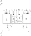
- FIG. 1A shows a circuit diagram of an exemplary embodiment of the present invention as a subsystem 102 of a system-on-chip (SoC) provided by a semiconductor integrated circuit device.
- the described subsystem comprises two identical general input/output (GPIO) circuits 104, 106 and an NFC interface circuit 108. These three circuits have shared access to two external connections in the form of pins 110, 112. More specifically, a first GPIO circuit 104 is connected to a first pin 110, a second GPIO circuit 106 is connected to a second pin 112, and the NFC interface circuit 108 is connected to both pins 110, 112.
- GPIO general input/output
- the GPIO circuits 104, 106 comprise a series of inputs and outputs 118, 120. These inputs and outputs 118, 120 are used for a variety of functions relating to the operation of the GPIO circuits 104, 106 such as sending and receiving data, enabling pull up or pull down resistors, etc.
- the NFC interface circuit 108 comprises a dual voltage clamp 114 and a variable resistance 116 that acts as part of a regulation loop which controls voltage across the pins when the NFC circuit is in its active mode.
- the voltage clamp 114 takes as inputs two enable signals 126, 128.
- a first 'enable clamp high' signal 126 enables the higher voltage clamp 114 which is set to permit a high supply voltage range, while a second 'enable clamp low' signal 128 enables the lower voltage clamp which is set at the lower limit of the design supply voltage range.
- the higher voltage clamp is set at 3.6V whereas the lower voltage clamp is set at 2.2V corresponding to the specified design voltage supply range of the device of 2.2V to 3.6V.
- the higher voltage clamp ensures that voltages across the pins 110, 112 never exceed values that would damage the device, whereas the lower voltage clamp, in a simple and power-efficient way, ensures that voltages across the pins 110, 112 never exceed the supply voltage when the NFC circuit is inactive for the complete device supply voltage range, even when the supply voltage is at its lower limit in the range.
- variable resistance 116 is used effectively to connect or disconnect the NFC circuit and also forms part of a regulation loop which controls voltage across the pins 110, 112 while the NFC circuit is active. It takes as its input a resistance control signal.
- the resistance control signal 130 comprises an n-bit word that can range in value from 0 to 2 n -1, which dictates the value of the variable resistance 116, wherein 0 indicates a high impedance (virtual open circuit) mode and 1 indicates a relatively high resistance, while 2 n -1 indicates low resistance.
- the NFC interface circuit 108 further comprises two NFC inputs for receiving data via NFC using an antenna connected across the two pins 110, 112 and sending said received data 122, 124 to a demodulation module, and two NFC outputs for sending data 134, 136 via NFC using the antenna.
- Figure 1B shows an effective circuit diagram of the embodiment of Fig 1A in a first mode of use.
- the pins 110, 112 have been connected to an NFC antenna 150 and the circuit is being operated in an NFC mode.
- the GPIO circuits 104, 106 have effectively been disconnected, leaving the pins 110, 112 connected only to the NFC interface circuit 108.
- Figure 1C shows an effective circuit diagram of the embodiment of Fig 1A in a second mode of use.
- the circuit is here being operated without connection to an NFC antenna and the NFC interface circuit 108 has effectively been disconnected, leaving the pins 110, 112 connected only to the GPIO circuits 104, 106. In this mode the voltage clamp 114 is disabled.
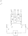
- FIG. 2 shows a circuit diagram of a second exemplary embodiment of the present invention as a subsystem 202 of a system-on-chip (SoC) provided by a semiconductor integrated circuit device.
- This embodiment is similar to the embodiments of Figures 1A to 1C , except that the NFC interface circuit 208 is connected to an NFC transmission and reception module 240.
- This NFC transmission and reception module 240 contains a number of amplifiers, filters etc. as required to transmit and receive NFC traffic via an NFC antenna 250 connected to the pins 210, 212 as would be expected by a person skilled in the art.
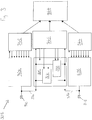
- FIG. 3 shows a circuit diagram of a further exemplary embodiment of the present invention as a subsystem 302 of a system-on-chip (SoC) provided by a semiconductor integrated circuit device.
- SoC system-on-chip
- This embodiment is similar to the embodiments of Figures 1A to 1C , except that the GPIO modules 304, 306 are each connected to a GPIO interface module 342, 344 and the NFC interface circuit 308 is connected to an NFC interface module 340.
- These interface modules 340, 342, 344 are each connected to a processor 346 that carries out the various operations required when the SoC 302 is being used either in a GPIO or NFC application.
- Figure 4 shows a timing diagram associated with the exemplary embodiment of Figure 1A which illustrates operation of the embodiments described above.
- Figure 4 depicts a steady, real supply voltage 400.
- a low voltage clamp threshold 402 which is set to the lowest allowed voltage in the design supply voltage range.
- the amplitude 404 of the voltage on the pins 110, 112 at any given moment in time is subject to change, depending on the current mode of operation of the system-on-chip 102, dictated by the state of the enable clamp low signal 128 and the resistance control signal 130.
- the system-on-chip 102 is in an NFC inactive mode.
- the low power, passive lower voltage clamp is enabled by setting the enable clamp low signal 128 to logic high.
- the variable resistance 116 is set to a high impedance mode by setting the resistance control signal 130 to 0.
- the amplitude 404 of the voltage is then clamped just below the low voltage clamp threshold.
- the system-on-chip 102 is switched into an NFC active mode for a duration 412.
- the enable clamp low signal 128 is set to logic low, which disables the low level voltage clamp.
- the resistance control signal 130 is switched from 0 to a non-high impedance value that varies with time such as to regulate the amplitude 404.
- the amplitude 404 is regulated by the active load (i.e. the variable resistance 116) to ramp up such that the amplitude 404 of the voltage across the pins 110, 112 lies close to the real supply voltage 400, i.e. NFC signals are able to make full use of the supply voltage range. This is achieved and subsequently maintained by the value of the resistance control signal 130 fluctuating in real-time to offset any detected difference between the amplitude 404 and the real supply voltage 400.
- the system-on-chip 102 is once again set to an NFC inactive mode for a duration 414.
- the enable clamp low signal 128 is set to logic high, re-enabling the low level voltage clamp, and the resistance control signal 130 is set to 0, thus setting the variable resistance 116 to a high impedance mode.
- the amplitude 404 does not undergo a ramp but instead is clipped to just under the low limit immediately.
- the enable clamp high signal 126 When an NFC antenna is connected, the enable clamp high signal 126 will be set to logic high to limit the voltage across the pins 110, 112 to the upper limit of the design supply voltage range such that the device cannot be damaged by high voltages regardless of any other settings.
- the enable clamp low signal 128 may be set to logic low for certain periods so that the variable resistance 116 can adjust the amplitude of the voltage swing to allow NFC signals to use the full supply voltage range, the upper limit clamp can remain on at all times in order to offer high voltage protection to the circuit without affecting the operation of the shunt regulation loop (i.e. the variable resistance 116).
- both the high and low limit clamps will be disabled by setting both the enable clamp high signal 126 and enable clamp low signal 128 to logic low. This reduces leakage between the pins 110, 112 and prevents short circuits if the pins 110, 112 are driven to different logic values.
Landscapes
- Engineering & Computer Science (AREA)
- Microelectronics & Electronic Packaging (AREA)
- Computer Hardware Design (AREA)
- Computer Networks & Wireless Communication (AREA)
- Physics & Mathematics (AREA)
- Signal Processing (AREA)
- General Physics & Mathematics (AREA)
- Theoretical Computer Science (AREA)
- Nonlinear Science (AREA)
- Semiconductor Integrated Circuits (AREA)
- Emergency Protection Circuit Devices (AREA)
- Logic Circuits (AREA)
- Near-Field Transmission Systems (AREA)
Description
- This invention relates to semiconductor integrated circuit devices, particularly multifunctional devices such as system-on-chip (SoC) devices.
- Modern semiconductor integrated circuits often implement an SoC arrangement, wherein a single integrated circuit may comprise the components typical of a computing system, i.e. a processor, memory, clock and external interfaces (e.g. USB, Ethernet, etc.), and wireless communication hardware. Such wireless communication hardware may be used for wireless communication protocols including wireless local area network (WLAN), Bluetooth (TM), and near field communications (NFC). In the case of NFC, a small loop antenna is connected to the integrated circuit and provides the SoC with the capability to communicate over short ranges using a local electric or magnetic field.
EP 2675077 which is regarded as closest prior art, discloses an NFC device which combines components of an antenna driver and a shunt regulator.US 2011/0215756 discloses an electronic device including a contactless charging function unit, a switching unit and a contactless integrated circuit card function unit which includes a clamp circuit. - NFC connectivity has become increasingly popular in recent times in mobile devices for short range communication and there is therefore demand for including this functionality in a system-on-chip implemented in an integrated semiconductor device. However the Applicant has recognised that it may not be required by all customers.
- From a first aspect, the invention provides a semiconductor integrated circuit device as claimed in claim 1.
- Thus it will be seen by those skilled in the art that, in accordance with the invention, a device is arranged such that the shared external connection, typically a pin, can be utilised for a plurality of functions, with voltage protection that may be appropriate for one function that can be enabled if required, but disabled for the other function which does not require it.
- A system-on-chip implemented in such an integrated semiconductor device typically comprises a number of pins that can be configured for a range of uses, including for general purpose input and output (GPIO) and for the connection of external peripherals to the integrated circuit. However, it is often the case that when these devices are fabricated, the purpose to which customers will put them is not known. Previously this meant that the manufacturer of a conventional system-on-chip device would either have to provide a wider product range to cater to a diverse range of end-user requirements, or provide a product with redundant connections corresponding to functions not used by all customers. In accordance with the invention however, customers not wishing to use the function provided by the first circuit may use the second circuit and vice versa. This optimises further the resources available from the device for all customers and so allows those not using a provided function to enjoy a compensatory benefit by making the shared external connection available for another use.
- In a set of embodiments the first circuit at least partly implements a near-field communication protocol and is configured to be connected to an external antenna via said shared external connection. Indeed the invention extends to an assembly comprising a device as hereinbefore described and an antenna connected to said shared external connection. In some embodiments for example, the integrated semiconductor device forms part of an emulated NFC tag.
- The second circuit comprises a general input/output interface such that the shared external connection can be used as a general input output connection. Such connections can have their function assigned by a user and can be used for both input and output. This is likely to maximise the flexibility of the device such that as many customers as possible can make use of all the connections available.
- In providing, in accordance with the invention, multiple circuits within an integrated semiconductor device that share at least one external connection, the Applicant has appreciated that those circuits may have different voltage range requirements for their operation. The Applicant has appreciated that providing a voltage clamp may allow whichever circuit is enabled to be operated safely by ensuring that components are not damaged by exposure to higher voltages, without having to increase power consumption or reduce performance.
- In a set of embodiments the device comprises two shared external connections. This would, for example, enable connection to an NFC antenna as set out above. In a set of such embodiments the voltage clamp is arranged to limit a maximum voltage that can be applied across said shared external connections. This would, for example, prevent excessive voltages which may develop across an attached NFC antenna from damaging the device whereas this may not be necessary when no antenna is connected. In a set of embodiments therefore the voltage clamp is enabled when an NFC circuit is enabled so as to allow an NFC antenna to be safely attached and the voltage clamp is disabled when an NFC circuit is disabled - e.g. when a general purpose input/output circuit is enabled.
- A single voltage clamp may be provided but in a set of embodiments at least two voltage clamps are provided with different clamp voltage values. Having two different voltage clamps is particularly beneficial where the circuit they protect can have an active and an inactive mode. During the inactive mode both of, or the lower of, the voltage clamps may be enabled, whereas in the active state only the higher voltage clamp is enabled. Preferably an alternative voltage control mechanism is employed in said active state. This means that good, simple protection is provided from the lower clamp value when the voltage across the shared external connections does not matter. When the circuit is active ultimate excess voltage protection is still provided but other, less limiting protection can be employed below this value.
- In an exemplary set of embodiments where, as is preferred, the circuit protected by the voltage clamps is an NFC circuit having active and inactive modes, in the inactive mode the lower voltage clamp is enabled but in the active mode the lower voltage clamp is disabled. In an exemplary set of embodiments the lower voltage clamp value is set at the lower end of a design supply voltage range. Where reference is made herein to a voltage clamp value being at the lower end of a design voltage range' it should be understood that this is not intended to limit the clamp value exactly to the lowest voltage in the design supply voltage range, but that the clamp value may be within a certain tolerance thereof. The voltage clamp value could, for example be within 20% of the lowest voltage in the design supply voltage range or within 10% of the lowest voltage in the design supply voltage range.
- Setting the clamp value at or close to the lowest intended supply voltage makes it possible to ensure that the actual supply voltage is not, or not significantly, exceeded in a simple, low power way compared to varying the clamp voltage according to an actual supply voltage which cannot necessarily be predicted (other than being assumed to be in the design supply voltage range).
- In a set of embodiments a regulation loop is provided to control the voltage across the shared external connections (and thus across the NFC antenna in the preferred embodiments) when the NFC circuit is in its active state. This allows the NFC circuit to use the full supply voltage which is actually available. This is important for optimal performance. The higher voltage clamp may simply provide backup protection against an absolute maximum voltage across the shared external connection. Such an arrangement provides the advantageous combination of low power consumption while the NFC circuit is in its inactive mode (which would usually be most of the time) and high performance when it is active.
- It should be understood that where reference is made to two voltage clamps these could be separate and independent or could be provided by a single mechanism which can have two values. It should also be understood that references to two clamps or voltages should not be interpreted as restrictive and therefore that further clamps or voltages could be provided.
- In some embodiments the regulation loop comprises a variable resistance. In a set of embodiments the regulation loop comprises a variable shunt resistance connected across the shared external connections.
- In a set of embodiments the integrated semiconductor device comprises a field detection circuit. In short range communication applications such as NFC, the Applicant has appreciated that it is advantageous to detect whether an appropriate electric or magnetic field is present before enabling the associated communication circuit within the system-on-chip. The field detection circuit may therefore be used to switch between the aforementioned active and inactive NFC modes.
- In modern mobile devices, it is advantageous to keep power requirements to a minimum. The Applicant has appreciated that the invention disclosed herein is particularly suited to such applications. In a set of embodiments the integrated semiconductor device is implemented in a battery powered integrated circuit.
- An embodiment of the present invention will now be described, by way of example only, with reference to the accompanying drawings, in which:
-
Figure 1A is a circuit diagram of a first exemplary embodiment of the present invention; -
Figure 1B is an effective circuit diagram of the embodiment ofFig 1A when operated in a first mode; -
Figure 1C is an effective circuit diagram of the embodiment ofFig 1A when operated in a second mode; -
Figure 2 is a circuit diagram of a second exemplary embodiment of the present invention; -
Figure 3 is a circuit diagram of a third exemplary embodiment of the present invention; and -
Figure 4 is a timing diagram associated with the exemplary embodiment ofFigure 1A . -
Figure 1A shows a circuit diagram of an exemplary embodiment of the present invention as a subsystem 102 of a system-on-chip (SoC) provided by a semiconductor integrated circuit device. The described subsystem comprises two identical general input/output (GPIO)circuits NFC interface circuit 108. These three circuits have shared access to two external connections in the form ofpins first GPIO circuit 104 is connected to afirst pin 110, asecond GPIO circuit 106 is connected to asecond pin 112, and theNFC interface circuit 108 is connected to bothpins - The
GPIO circuits GPIO circuits - The
NFC interface circuit 108 comprises adual voltage clamp 114 and avariable resistance 116 that acts as part of a regulation loop which controls voltage across the pins when the NFC circuit is in its active mode. Thevoltage clamp 114 takes as inputs two enablesignals signal 126 enables thehigher voltage clamp 114 which is set to permit a high supply voltage range, while a second 'enable clamp low'signal 128 enables the lower voltage clamp which is set at the lower limit of the design supply voltage range. In one particular non-limiting example the higher voltage clamp is set at 3.6V whereas the lower voltage clamp is set at 2.2V corresponding to the specified design voltage supply range of the device of 2.2V to 3.6V. The higher voltage clamp ensures that voltages across thepins pins - As will be described in more detail below, the
variable resistance 116 is used effectively to connect or disconnect the NFC circuit and also forms part of a regulation loop which controls voltage across thepins resistance control signal 130 comprises an n-bit word that can range in value from 0 to 2n-1, which dictates the value of thevariable resistance 116, wherein 0 indicates a high impedance (virtual open circuit) mode and 1 indicates a relatively high resistance, while 2n-1 indicates low resistance. - The
NFC interface circuit 108 further comprises two NFC inputs for receiving data via NFC using an antenna connected across the twopins data 122, 124 to a demodulation module, and two NFC outputs for sendingdata -
Figure 1B shows an effective circuit diagram of the embodiment ofFig 1A in a first mode of use. Thepins NFC antenna 150 and the circuit is being operated in an NFC mode. As such, theGPIO circuits pins NFC interface circuit 108. -
Figure 1C shows an effective circuit diagram of the embodiment ofFig 1A in a second mode of use. The circuit is here being operated without connection to an NFC antenna and theNFC interface circuit 108 has effectively been disconnected, leaving thepins GPIO circuits voltage clamp 114 is disabled. -
Figure 2 shows a circuit diagram of a second exemplary embodiment of the present invention as asubsystem 202 of a system-on-chip (SoC) provided by a semiconductor integrated circuit device. This embodiment is similar to the embodiments ofFigures 1A to 1C , except that theNFC interface circuit 208 is connected to an NFC transmission andreception module 240. This NFC transmission andreception module 240 contains a number of amplifiers, filters etc. as required to transmit and receive NFC traffic via anNFC antenna 250 connected to thepins -
Figure 3 shows a circuit diagram of a further exemplary embodiment of the present invention as asubsystem 302 of a system-on-chip (SoC) provided by a semiconductor integrated circuit device. This embodiment is similar to the embodiments ofFigures 1A to 1C , except that theGPIO modules GPIO interface module NFC interface circuit 308 is connected to anNFC interface module 340. Theseinterface modules processor 346 that carries out the various operations required when theSoC 302 is being used either in a GPIO or NFC application. -
Figure 4 shows a timing diagram associated with the exemplary embodiment ofFigure 1A which illustrates operation of the embodiments described above.Figure 4 depicts a steady,real supply voltage 400. There is also a lowvoltage clamp threshold 402, which is set to the lowest allowed voltage in the design supply voltage range. - The
amplitude 404 of the voltage on thepins low signal 128 and theresistance control signal 130. - For an
initial duration 410, the system-on-chip 102 is in an NFC inactive mode. During this time, the low power, passive lower voltage clamp is enabled by setting the enable clamplow signal 128 to logic high. Accordingly, thevariable resistance 116 is set to a high impedance mode by setting theresistance control signal 130 to 0. Theamplitude 404 of the voltage is then clamped just below the low voltage clamp threshold. - At the end of
duration 410 attime 416, the system-on-chip 102 is switched into an NFC active mode for aduration 412. At thistime 416, the enable clamplow signal 128 is set to logic low, which disables the low level voltage clamp. Simultaneously or slightly before this, theresistance control signal 130 is switched from 0 to a non-high impedance value that varies with time such as to regulate theamplitude 404. When this switch occurs, theamplitude 404 is regulated by the active load (i.e. the variable resistance 116) to ramp up such that theamplitude 404 of the voltage across thepins real supply voltage 400, i.e. NFC signals are able to make full use of the supply voltage range. This is achieved and subsequently maintained by the value of theresistance control signal 130 fluctuating in real-time to offset any detected difference between theamplitude 404 and thereal supply voltage 400. - At a
subsequent time 418 at the end ofduration 412, the system-on-chip 102 is once again set to an NFC inactive mode for a duration 414. At thistime 418, the enable clamplow signal 128 is set to logic high, re-enabling the low level voltage clamp, and theresistance control signal 130 is set to 0, thus setting thevariable resistance 116 to a high impedance mode. It is noteworthy that unlike when switching to an NFC active mode, theamplitude 404 does not undergo a ramp but instead is clipped to just under the low limit immediately. - When an NFC antenna is connected, the enable clamp
high signal 126 will be set to logic high to limit the voltage across thepins low signal 128 may be set to logic low for certain periods so that thevariable resistance 116 can adjust the amplitude of the voltage swing to allow NFC signals to use the full supply voltage range, the upper limit clamp can remain on at all times in order to offer high voltage protection to the circuit without affecting the operation of the shunt regulation loop (i.e. the variable resistance 116). - When the system-on-chip 102 is to be used only for digital GPIO purposes (i.e. no antenna will be connected to the
pins 110, 112), both the high and low limit clamps will be disabled by setting both the enable clamphigh signal 126 and enable clamplow signal 128 to logic low. This reduces leakage between thepins pins - Thus it will be seen that a system-on-chip that shares pins between multiple circuits has been described. When a voltage clamp is used it is possible to adjust the circuit to utilise the full range of a time-varying supply voltage when needed and employ a more restrictive clamp when it is not needed to save power. Although particular embodiments have been described in detail, many variations and modifications are possible within the scope of the invention.
Claims (15)
- A semiconductor integrated circuit device comprising at least first and second circuits (104, 106, 108), said first and second circuits (104, 106, 108) being connected to a shared external connection (110, 112), said device further comprising a voltage clamp (114) that is operable to limit a voltage at the shared external connection (110, 112), wherein said voltage clamp (114) can be selectively enabled depending upon whether said first or second circuit (104, 106, 108) is being used and characterised in that the second circuit (104, 106) comprises a general input/output interface such that the shared external connection (110, 112) can be used as a general input output connection .
- A semiconductor integrated circuit device (102) as claimed in claim 1 wherein the first circuit (108) at least partly implements a near-field communication protocol and is configured to be connected to an external antenna (150) via said shared external connection (110, 112).
- A semiconductor integrated circuit device (102) as claimed in claim 1 or 2 forming part of an emulated NFC tag.
- A semiconductor integrated circuit device (102) as claimed in any preceding claim wherein the voltage clamp (114) is enabled when an NFC circuit is enabled so as to allow an NFC antenna (150) to be safely attached and the voltage clamp (114) is disabled when an NFC circuit is disabled.
- A semiconductor integrated circuit device (102) as claimed in any preceding claim wherein the device comprises two shared external connections (110, 112).
- A semiconductor integrated circuit device (102) as claimed in claim 5 wherein the voltage clamp (114) is arranged to limit a maximum voltage that can be applied across said shared external connections (110, 112).
- A semiconductor integrated circuit device (102) as claimed in claim 6 wherein at least two voltage clamps (114) are provided with different clamp voltage values.
- A semiconductor integrated circuit device (102) as claimed in claim 7 wherein the circuit protected by the voltage clamps (114) is a circuit having active and inactive modes,
preferably wherein the lower voltage clamp is enabled in the inactive mode but in the active mode the lower voltage clamp is disabled. - A semiconductor integrated circuit device (102) as claimed in claim 8 comprising an alternative voltage control for controlling a voltage across the external connections in said active mode.
- A semiconductor integrated circuit device (102) as claimed in claim 9 wherein the alternative voltage control comprises a regulation loop,
preferably wherein the regulation loop comprises a variable resistance (116). - A semiconductor integrated circuit device (102) as claimed in claim 10 wherein the regulation loop comprises a variable shunt resistance (116) connected across the shared external connections (110, 112).
- A semiconductor integrated circuit device (102) as claimed in any of claims 7 to 11 wherein the lower voltage clamp value is set at the lower end of a design supply voltage range.
- A semiconductor integrated circuit device (102) as claimed in any preceding claim wherein the integrated semiconductor device comprises a field detection circuit.
- A battery powered integrated circuit comprising a semiconductor integrated circuit device (102) as claimed in any of claims 1 to 13.
- An assembly comprising a semiconductor integrated circuit device (102) as claimed in any of claims 1 to 13 and an antenna (150) connected to said shared external connection (110, 112).
Applications Claiming Priority (2)
| Application Number | Priority Date | Filing Date | Title |
|---|---|---|---|
| GB1422818.3A GB2533421A (en) | 2014-12-19 | 2014-12-19 | Integrated circuits |
| PCT/GB2015/053978 WO2016097710A1 (en) | 2014-12-19 | 2015-12-14 | Integrated circuits |
Publications (2)
| Publication Number | Publication Date |
|---|---|
| EP3235090A1 EP3235090A1 (en) | 2017-10-25 |
| EP3235090B1 true EP3235090B1 (en) | 2021-02-17 |
Family
ID=54937278
Family Applications (1)
| Application Number | Title | Priority Date | Filing Date |
|---|---|---|---|
| EP15813521.0A Active EP3235090B1 (en) | 2014-12-19 | 2015-12-14 | Integrated circuits |
Country Status (8)
| Country | Link |
|---|---|
| US (1) | US10727667B2 (en) |
| EP (1) | EP3235090B1 (en) |
| JP (1) | JP2018502544A (en) |
| KR (1) | KR20170096184A (en) |
| CN (1) | CN107111775B (en) |
| GB (1) | GB2533421A (en) |
| TW (1) | TW201633218A (en) |
| WO (1) | WO2016097710A1 (en) |
Families Citing this family (2)
| Publication number | Priority date | Publication date | Assignee | Title |
|---|---|---|---|---|
| JP7459583B2 (en) * | 2020-03-17 | 2024-04-02 | 住友電装株式会社 | Wiring materials |
| US20240132485A1 (en) * | 2020-10-16 | 2024-04-25 | Cemm - Forschungszentrum Für Molekulare Medizin Gmbh | Heterocyclic cullin ring ubiquitin ligase compounds and uses thereof |
Family Cites Families (9)
| Publication number | Priority date | Publication date | Assignee | Title |
|---|---|---|---|---|
| GB0505060D0 (en) * | 2005-03-11 | 2005-04-20 | Innovision Res & Tech Plc | Gain controlled impedance |
| JP2006302971A (en) * | 2005-04-15 | 2006-11-02 | Fujitsu Ltd | Power supply clamp circuit and semiconductor device |
| US7902654B2 (en) * | 2006-05-10 | 2011-03-08 | Qualcomm Incorporated | System and method of silicon switched power delivery using a package |
| KR100814437B1 (en) * | 2006-11-03 | 2008-03-17 | 삼성전자주식회사 | Hybrid Electrostatic Discharge Protection Circuit |
| US20100002345A1 (en) * | 2008-07-02 | 2010-01-07 | Skyworks Solutions, Inc. | Radio frequency switch electrostatic discharge protection circuit |
| GB2464538A (en) * | 2008-10-17 | 2010-04-28 | Cambridge Silicon Radio Ltd | An ESD protection circuit for a transmitter output |
| US8536828B2 (en) * | 2010-03-02 | 2013-09-17 | Sony Corporation | Coordinating contactless communication and charging functions |
| CN202353591U (en) * | 2011-11-29 | 2012-07-25 | 冯海青 | Near field communication (NFC) chip |
| US9020424B2 (en) * | 2012-06-14 | 2015-04-28 | Broadcom Corporation | NFC device combining components of antenna driver and shunt regulator |
-
2014
- 2014-12-19 GB GB1422818.3A patent/GB2533421A/en not_active Withdrawn
-
2015
- 2015-12-11 TW TW104141767A patent/TW201633218A/en unknown
- 2015-12-14 EP EP15813521.0A patent/EP3235090B1/en active Active
- 2015-12-14 WO PCT/GB2015/053978 patent/WO2016097710A1/en not_active Ceased
- 2015-12-14 US US15/537,631 patent/US10727667B2/en active Active
- 2015-12-14 CN CN201580068597.6A patent/CN107111775B/en active Active
- 2015-12-14 JP JP2017532672A patent/JP2018502544A/en active Pending
- 2015-12-14 KR KR1020177020101A patent/KR20170096184A/en not_active Withdrawn
Non-Patent Citations (1)
| Title |
|---|
| None * |
Also Published As
| Publication number | Publication date |
|---|---|
| CN107111775B (en) | 2020-09-04 |
| TW201633218A (en) | 2016-09-16 |
| US20170353029A1 (en) | 2017-12-07 |
| CN107111775A (en) | 2017-08-29 |
| EP3235090A1 (en) | 2017-10-25 |
| WO2016097710A1 (en) | 2016-06-23 |
| GB2533421A (en) | 2016-06-22 |
| KR20170096184A (en) | 2017-08-23 |
| JP2018502544A (en) | 2018-01-25 |
| US10727667B2 (en) | 2020-07-28 |
Similar Documents
| Publication | Publication Date | Title |
|---|---|---|
| EP3609049B1 (en) | Wireless charging device and wireless charging method | |
| US10574073B2 (en) | Electronic device and method for controlling power supply | |
| US10423205B2 (en) | Voltage transition control for USB power delivery sources | |
| US20150035477A1 (en) | Method and apparatus of fast battery charging with universal high power input source | |
| US8692520B2 (en) | Method and system for optimizing current limiting behavior of charger | |
| US9711975B2 (en) | Power bank circuit and the method thereof | |
| US20130169059A1 (en) | Dual Input Single Output Power Multiplexer for Near Field Communication Application | |
| GB2479792A (en) | Near Field RF Commuincator | |
| EP3664368B1 (en) | Power sourcing equipment and energy-saving method for power over ethernet | |
| JP2012213250A (en) | Protection circuit and input/output circuit | |
| CN106655316A (en) | Charging circuit and terminal equipment | |
| US10079688B2 (en) | Network port and ethernet device integrating powered device and power sourcing equivalent in a port | |
| WO2018064102A2 (en) | Systems and methods for power control | |
| CN103166251B (en) | Backup Battery Charging Circuit | |
| US9459675B2 (en) | Multi-battery power supply system | |
| US10727667B2 (en) | Integrated circuits | |
| WO2016141572A1 (en) | Leakage current detection circuit of terminal, and terminal | |
| CN110912239B (en) | A multi-port charging device | |
| KR102371501B1 (en) | Apparatus and method for providing usb interface between potable device and external device | |
| US9209651B2 (en) | VBUS power switch | |
| CN204904053U (en) | Automatic load option function module | |
| WO2022222439A1 (en) | Communication device and system, and communication method | |
| EP2972923B1 (en) | Combined power and input/output line | |
| TWI716244B (en) | Power supply device and power supply method | |
| CN108808868A (en) | wireless charging receiving device with voltage protection |
Legal Events
| Date | Code | Title | Description |
|---|---|---|---|
| STAA | Information on the status of an ep patent application or granted ep patent |
Free format text: STATUS: THE INTERNATIONAL PUBLICATION HAS BEEN MADE |
|
| PUAI | Public reference made under article 153(3) epc to a published international application that has entered the european phase |
Free format text: ORIGINAL CODE: 0009012 |
|
| STAA | Information on the status of an ep patent application or granted ep patent |
Free format text: STATUS: REQUEST FOR EXAMINATION WAS MADE |
|
| 17P | Request for examination filed |
Effective date: 20170717 |
|
| AK | Designated contracting states |
Kind code of ref document: A1 Designated state(s): AL AT BE BG CH CY CZ DE DK EE ES FI FR GB GR HR HU IE IS IT LI LT LU LV MC MK MT NL NO PL PT RO RS SE SI SK SM TR |
|
| AX | Request for extension of the european patent |
Extension state: BA ME |
|
| DAV | Request for validation of the european patent (deleted) | ||
| DAX | Request for extension of the european patent (deleted) | ||
| STAA | Information on the status of an ep patent application or granted ep patent |
Free format text: STATUS: EXAMINATION IS IN PROGRESS |
|
| 17Q | First examination report despatched |
Effective date: 20190624 |
|
| GRAP | Despatch of communication of intention to grant a patent |
Free format text: ORIGINAL CODE: EPIDOSNIGR1 |
|
| STAA | Information on the status of an ep patent application or granted ep patent |
Free format text: STATUS: GRANT OF PATENT IS INTENDED |
|
| INTG | Intention to grant announced |
Effective date: 20201106 |
|
| GRAS | Grant fee paid |
Free format text: ORIGINAL CODE: EPIDOSNIGR3 |
|
| GRAA | (expected) grant |
Free format text: ORIGINAL CODE: 0009210 |
|
| STAA | Information on the status of an ep patent application or granted ep patent |
Free format text: STATUS: THE PATENT HAS BEEN GRANTED |
|
| AK | Designated contracting states |
Kind code of ref document: B1 Designated state(s): AL AT BE BG CH CY CZ DE DK EE ES FI FR GB GR HR HU IE IS IT LI LT LU LV MC MK MT NL NO PL PT RO RS SE SI SK SM TR |
|
| REG | Reference to a national code |
Ref country code: GB Ref legal event code: FG4D |
|
| REG | Reference to a national code |
Ref country code: CH Ref legal event code: EP |
|
| REG | Reference to a national code |
Ref country code: DE Ref legal event code: R096 Ref document number: 602015065712 Country of ref document: DE |
|
| REG | Reference to a national code |
Ref country code: AT Ref legal event code: REF Ref document number: 1362738 Country of ref document: AT Kind code of ref document: T Effective date: 20210315 |
|
| REG | Reference to a national code |
Ref country code: IE Ref legal event code: FG4D |
|
| REG | Reference to a national code |
Ref country code: LT Ref legal event code: MG9D |
|
| REG | Reference to a national code |
Ref country code: NL Ref legal event code: MP Effective date: 20210217 |
|
| PG25 | Lapsed in a contracting state [announced via postgrant information from national office to epo] |
Ref country code: NO Free format text: LAPSE BECAUSE OF FAILURE TO SUBMIT A TRANSLATION OF THE DESCRIPTION OR TO PAY THE FEE WITHIN THE PRESCRIBED TIME-LIMIT Effective date: 20210517 Ref country code: PT Free format text: LAPSE BECAUSE OF FAILURE TO SUBMIT A TRANSLATION OF THE DESCRIPTION OR TO PAY THE FEE WITHIN THE PRESCRIBED TIME-LIMIT Effective date: 20210617 Ref country code: LT Free format text: LAPSE BECAUSE OF FAILURE TO SUBMIT A TRANSLATION OF THE DESCRIPTION OR TO PAY THE FEE WITHIN THE PRESCRIBED TIME-LIMIT Effective date: 20210217 Ref country code: FI Free format text: LAPSE BECAUSE OF FAILURE TO SUBMIT A TRANSLATION OF THE DESCRIPTION OR TO PAY THE FEE WITHIN THE PRESCRIBED TIME-LIMIT Effective date: 20210217 Ref country code: GR Free format text: LAPSE BECAUSE OF FAILURE TO SUBMIT A TRANSLATION OF THE DESCRIPTION OR TO PAY THE FEE WITHIN THE PRESCRIBED TIME-LIMIT Effective date: 20210518 Ref country code: HR Free format text: LAPSE BECAUSE OF FAILURE TO SUBMIT A TRANSLATION OF THE DESCRIPTION OR TO PAY THE FEE WITHIN THE PRESCRIBED TIME-LIMIT Effective date: 20210217 Ref country code: BG Free format text: LAPSE BECAUSE OF FAILURE TO SUBMIT A TRANSLATION OF THE DESCRIPTION OR TO PAY THE FEE WITHIN THE PRESCRIBED TIME-LIMIT Effective date: 20210517 |
|
| REG | Reference to a national code |
Ref country code: AT Ref legal event code: MK05 Ref document number: 1362738 Country of ref document: AT Kind code of ref document: T Effective date: 20210217 |
|
| PG25 | Lapsed in a contracting state [announced via postgrant information from national office to epo] |
Ref country code: SE Free format text: LAPSE BECAUSE OF FAILURE TO SUBMIT A TRANSLATION OF THE DESCRIPTION OR TO PAY THE FEE WITHIN THE PRESCRIBED TIME-LIMIT Effective date: 20210217 Ref country code: RS Free format text: LAPSE BECAUSE OF FAILURE TO SUBMIT A TRANSLATION OF THE DESCRIPTION OR TO PAY THE FEE WITHIN THE PRESCRIBED TIME-LIMIT Effective date: 20210217 Ref country code: PL Free format text: LAPSE BECAUSE OF FAILURE TO SUBMIT A TRANSLATION OF THE DESCRIPTION OR TO PAY THE FEE WITHIN THE PRESCRIBED TIME-LIMIT Effective date: 20210217 Ref country code: NL Free format text: LAPSE BECAUSE OF FAILURE TO SUBMIT A TRANSLATION OF THE DESCRIPTION OR TO PAY THE FEE WITHIN THE PRESCRIBED TIME-LIMIT Effective date: 20210217 Ref country code: LV Free format text: LAPSE BECAUSE OF FAILURE TO SUBMIT A TRANSLATION OF THE DESCRIPTION OR TO PAY THE FEE WITHIN THE PRESCRIBED TIME-LIMIT Effective date: 20210217 |
|
| PG25 | Lapsed in a contracting state [announced via postgrant information from national office to epo] |
Ref country code: IS Free format text: LAPSE BECAUSE OF FAILURE TO SUBMIT A TRANSLATION OF THE DESCRIPTION OR TO PAY THE FEE WITHIN THE PRESCRIBED TIME-LIMIT Effective date: 20210617 |
|
| PG25 | Lapsed in a contracting state [announced via postgrant information from national office to epo] |
Ref country code: SM Free format text: LAPSE BECAUSE OF FAILURE TO SUBMIT A TRANSLATION OF THE DESCRIPTION OR TO PAY THE FEE WITHIN THE PRESCRIBED TIME-LIMIT Effective date: 20210217 Ref country code: AT Free format text: LAPSE BECAUSE OF FAILURE TO SUBMIT A TRANSLATION OF THE DESCRIPTION OR TO PAY THE FEE WITHIN THE PRESCRIBED TIME-LIMIT Effective date: 20210217 Ref country code: EE Free format text: LAPSE BECAUSE OF FAILURE TO SUBMIT A TRANSLATION OF THE DESCRIPTION OR TO PAY THE FEE WITHIN THE PRESCRIBED TIME-LIMIT Effective date: 20210217 Ref country code: CZ Free format text: LAPSE BECAUSE OF FAILURE TO SUBMIT A TRANSLATION OF THE DESCRIPTION OR TO PAY THE FEE WITHIN THE PRESCRIBED TIME-LIMIT Effective date: 20210217 |
|
| REG | Reference to a national code |
Ref country code: DE Ref legal event code: R097 Ref document number: 602015065712 Country of ref document: DE |
|
| PG25 | Lapsed in a contracting state [announced via postgrant information from national office to epo] |
Ref country code: SK Free format text: LAPSE BECAUSE OF FAILURE TO SUBMIT A TRANSLATION OF THE DESCRIPTION OR TO PAY THE FEE WITHIN THE PRESCRIBED TIME-LIMIT Effective date: 20210217 Ref country code: RO Free format text: LAPSE BECAUSE OF FAILURE TO SUBMIT A TRANSLATION OF THE DESCRIPTION OR TO PAY THE FEE WITHIN THE PRESCRIBED TIME-LIMIT Effective date: 20210217 Ref country code: DK Free format text: LAPSE BECAUSE OF FAILURE TO SUBMIT A TRANSLATION OF THE DESCRIPTION OR TO PAY THE FEE WITHIN THE PRESCRIBED TIME-LIMIT Effective date: 20210217 |
|
| PLBE | No opposition filed within time limit |
Free format text: ORIGINAL CODE: 0009261 |
|
| STAA | Information on the status of an ep patent application or granted ep patent |
Free format text: STATUS: NO OPPOSITION FILED WITHIN TIME LIMIT |
|
| 26N | No opposition filed |
Effective date: 20211118 |
|
| PG25 | Lapsed in a contracting state [announced via postgrant information from national office to epo] |
Ref country code: AL Free format text: LAPSE BECAUSE OF FAILURE TO SUBMIT A TRANSLATION OF THE DESCRIPTION OR TO PAY THE FEE WITHIN THE PRESCRIBED TIME-LIMIT Effective date: 20210217 Ref country code: ES Free format text: LAPSE BECAUSE OF FAILURE TO SUBMIT A TRANSLATION OF THE DESCRIPTION OR TO PAY THE FEE WITHIN THE PRESCRIBED TIME-LIMIT Effective date: 20210217 |
|
| PG25 | Lapsed in a contracting state [announced via postgrant information from national office to epo] |
Ref country code: SI Free format text: LAPSE BECAUSE OF FAILURE TO SUBMIT A TRANSLATION OF THE DESCRIPTION OR TO PAY THE FEE WITHIN THE PRESCRIBED TIME-LIMIT Effective date: 20210217 |
|
| PG25 | Lapsed in a contracting state [announced via postgrant information from national office to epo] |
Ref country code: IT Free format text: LAPSE BECAUSE OF FAILURE TO SUBMIT A TRANSLATION OF THE DESCRIPTION OR TO PAY THE FEE WITHIN THE PRESCRIBED TIME-LIMIT Effective date: 20210217 |
|
| PG25 | Lapsed in a contracting state [announced via postgrant information from national office to epo] |
Ref country code: IS Free format text: LAPSE BECAUSE OF FAILURE TO SUBMIT A TRANSLATION OF THE DESCRIPTION OR TO PAY THE FEE WITHIN THE PRESCRIBED TIME-LIMIT Effective date: 20210617 |
|
| PG25 | Lapsed in a contracting state [announced via postgrant information from national office to epo] |
Ref country code: MC Free format text: LAPSE BECAUSE OF FAILURE TO SUBMIT A TRANSLATION OF THE DESCRIPTION OR TO PAY THE FEE WITHIN THE PRESCRIBED TIME-LIMIT Effective date: 20210217 |
|
| REG | Reference to a national code |
Ref country code: CH Ref legal event code: PL |
|
| REG | Reference to a national code |
Ref country code: BE Ref legal event code: MM Effective date: 20211231 |
|
| PG25 | Lapsed in a contracting state [announced via postgrant information from national office to epo] |
Ref country code: LU Free format text: LAPSE BECAUSE OF NON-PAYMENT OF DUE FEES Effective date: 20211214 Ref country code: IE Free format text: LAPSE BECAUSE OF NON-PAYMENT OF DUE FEES Effective date: 20211214 |
|
| PG25 | Lapsed in a contracting state [announced via postgrant information from national office to epo] |
Ref country code: BE Free format text: LAPSE BECAUSE OF NON-PAYMENT OF DUE FEES Effective date: 20211231 |
|
| PG25 | Lapsed in a contracting state [announced via postgrant information from national office to epo] |
Ref country code: LI Free format text: LAPSE BECAUSE OF NON-PAYMENT OF DUE FEES Effective date: 20211231 Ref country code: CH Free format text: LAPSE BECAUSE OF NON-PAYMENT OF DUE FEES Effective date: 20211231 |
|
| PG25 | Lapsed in a contracting state [announced via postgrant information from national office to epo] |
Ref country code: HU Free format text: LAPSE BECAUSE OF FAILURE TO SUBMIT A TRANSLATION OF THE DESCRIPTION OR TO PAY THE FEE WITHIN THE PRESCRIBED TIME-LIMIT; INVALID AB INITIO Effective date: 20151214 |
|
| PG25 | Lapsed in a contracting state [announced via postgrant information from national office to epo] |
Ref country code: CY Free format text: LAPSE BECAUSE OF FAILURE TO SUBMIT A TRANSLATION OF THE DESCRIPTION OR TO PAY THE FEE WITHIN THE PRESCRIBED TIME-LIMIT Effective date: 20210217 |
|
| PG25 | Lapsed in a contracting state [announced via postgrant information from national office to epo] |
Ref country code: MK Free format text: LAPSE BECAUSE OF FAILURE TO SUBMIT A TRANSLATION OF THE DESCRIPTION OR TO PAY THE FEE WITHIN THE PRESCRIBED TIME-LIMIT Effective date: 20210217 |
|
| PG25 | Lapsed in a contracting state [announced via postgrant information from national office to epo] |
Ref country code: TR Free format text: LAPSE BECAUSE OF FAILURE TO SUBMIT A TRANSLATION OF THE DESCRIPTION OR TO PAY THE FEE WITHIN THE PRESCRIBED TIME-LIMIT Effective date: 20210217 |
|
| PG25 | Lapsed in a contracting state [announced via postgrant information from national office to epo] |
Ref country code: MT Free format text: LAPSE BECAUSE OF FAILURE TO SUBMIT A TRANSLATION OF THE DESCRIPTION OR TO PAY THE FEE WITHIN THE PRESCRIBED TIME-LIMIT Effective date: 20210217 |
|
| PGFP | Annual fee paid to national office [announced via postgrant information from national office to epo] |
Ref country code: DE Payment date: 20251126 Year of fee payment: 11 |
|
| PGFP | Annual fee paid to national office [announced via postgrant information from national office to epo] |
Ref country code: GB Payment date: 20251120 Year of fee payment: 11 |
|
| PGFP | Annual fee paid to national office [announced via postgrant information from national office to epo] |
Ref country code: FR Payment date: 20251120 Year of fee payment: 11 |