EP3232580A1 - Touch screen integrated with nfc antenna, terminal, and near field communication method therefor - Google Patents
Touch screen integrated with nfc antenna, terminal, and near field communication method therefor Download PDFInfo
- Publication number
- EP3232580A1 EP3232580A1 EP15866742.8A EP15866742A EP3232580A1 EP 3232580 A1 EP3232580 A1 EP 3232580A1 EP 15866742 A EP15866742 A EP 15866742A EP 3232580 A1 EP3232580 A1 EP 3232580A1
- Authority
- EP
- European Patent Office
- Prior art keywords
- module
- screen
- terminal
- near field
- field communication
- Prior art date
- Legal status (The legal status is an assumption and is not a legal conclusion. Google has not performed a legal analysis and makes no representation as to the accuracy of the status listed.)
- Granted
Links
Images
Classifications
-
- H—ELECTRICITY
- H04—ELECTRIC COMMUNICATION TECHNIQUE
- H04B—TRANSMISSION
- H04B5/00—Near-field transmission systems, e.g. inductive or capacitive transmission systems
- H04B5/70—Near-field transmission systems, e.g. inductive or capacitive transmission systems specially adapted for specific purposes
- H04B5/72—Near-field transmission systems, e.g. inductive or capacitive transmission systems specially adapted for specific purposes for local intradevice communication
-
- G—PHYSICS
- G06—COMPUTING OR CALCULATING; COUNTING
- G06F—ELECTRIC DIGITAL DATA PROCESSING
- G06F3/00—Input arrangements for transferring data to be processed into a form capable of being handled by the computer; Output arrangements for transferring data from processing unit to output unit, e.g. interface arrangements
- G06F3/01—Input arrangements or combined input and output arrangements for interaction between user and computer
- G06F3/03—Arrangements for converting the position or the displacement of a member into a coded form
- G06F3/041—Digitisers, e.g. for touch screens or touch pads, characterised by the transducing means
- G06F3/0416—Control or interface arrangements specially adapted for digitisers
-
- G—PHYSICS
- G06—COMPUTING OR CALCULATING; COUNTING
- G06F—ELECTRIC DIGITAL DATA PROCESSING
- G06F3/00—Input arrangements for transferring data to be processed into a form capable of being handled by the computer; Output arrangements for transferring data from processing unit to output unit, e.g. interface arrangements
- G06F3/01—Input arrangements or combined input and output arrangements for interaction between user and computer
- G06F3/03—Arrangements for converting the position or the displacement of a member into a coded form
- G06F3/041—Digitisers, e.g. for touch screens or touch pads, characterised by the transducing means
-
- G—PHYSICS
- G06—COMPUTING OR CALCULATING; COUNTING
- G06F—ELECTRIC DIGITAL DATA PROCESSING
- G06F3/00—Input arrangements for transferring data to be processed into a form capable of being handled by the computer; Output arrangements for transferring data from processing unit to output unit, e.g. interface arrangements
- G06F3/01—Input arrangements or combined input and output arrangements for interaction between user and computer
- G06F3/03—Arrangements for converting the position or the displacement of a member into a coded form
- G06F3/041—Digitisers, e.g. for touch screens or touch pads, characterised by the transducing means
- G06F3/0412—Digitisers structurally integrated in a display
-
- G—PHYSICS
- G06—COMPUTING OR CALCULATING; COUNTING
- G06F—ELECTRIC DIGITAL DATA PROCESSING
- G06F3/00—Input arrangements for transferring data to be processed into a form capable of being handled by the computer; Output arrangements for transferring data from processing unit to output unit, e.g. interface arrangements
- G06F3/01—Input arrangements or combined input and output arrangements for interaction between user and computer
- G06F3/03—Arrangements for converting the position or the displacement of a member into a coded form
- G06F3/041—Digitisers, e.g. for touch screens or touch pads, characterised by the transducing means
- G06F3/047—Digitisers, e.g. for touch screens or touch pads, characterised by the transducing means using sets of wires, e.g. crossed wires
-
- H—ELECTRICITY
- H01—ELECTRIC ELEMENTS
- H01Q—ANTENNAS, i.e. RADIO AERIALS
- H01Q1/00—Details of, or arrangements associated with, antennas
- H01Q1/12—Supports; Mounting means
- H01Q1/22—Supports; Mounting means by structural association with other equipment or articles
- H01Q1/2208—Supports; Mounting means by structural association with other equipment or articles associated with components used in interrogation type services, i.e. in systems for information exchange between an interrogator/reader and a tag/transponder, e.g. in Radio Frequency Identification [RFID] systems
-
- H—ELECTRICITY
- H01—ELECTRIC ELEMENTS
- H01Q—ANTENNAS, i.e. RADIO AERIALS
- H01Q1/00—Details of, or arrangements associated with, antennas
- H01Q1/12—Supports; Mounting means
- H01Q1/22—Supports; Mounting means by structural association with other equipment or articles
- H01Q1/2258—Supports; Mounting means by structural association with other equipment or articles used with computer equipment
- H01Q1/2266—Supports; Mounting means by structural association with other equipment or articles used with computer equipment disposed inside the computer
-
- H—ELECTRICITY
- H01—ELECTRIC ELEMENTS
- H01Q—ANTENNAS, i.e. RADIO AERIALS
- H01Q1/00—Details of, or arrangements associated with, antennas
- H01Q1/12—Supports; Mounting means
- H01Q1/22—Supports; Mounting means by structural association with other equipment or articles
- H01Q1/24—Supports; Mounting means by structural association with other equipment or articles with receiving set
- H01Q1/241—Supports; Mounting means by structural association with other equipment or articles with receiving set used in mobile communications, e.g. GSM
- H01Q1/242—Supports; Mounting means by structural association with other equipment or articles with receiving set used in mobile communications, e.g. GSM specially adapted for hand-held use
- H01Q1/243—Supports; Mounting means by structural association with other equipment or articles with receiving set used in mobile communications, e.g. GSM specially adapted for hand-held use with built-in antennas
-
- H—ELECTRICITY
- H01—ELECTRIC ELEMENTS
- H01Q—ANTENNAS, i.e. RADIO AERIALS
- H01Q1/00—Details of, or arrangements associated with, antennas
- H01Q1/44—Details of, or arrangements associated with, antennas using equipment having another main function to serve additionally as an antenna, e.g. means for giving an antenna an aesthetic aspect
-
- H—ELECTRICITY
- H01—ELECTRIC ELEMENTS
- H01Q—ANTENNAS, i.e. RADIO AERIALS
- H01Q1/00—Details of, or arrangements associated with, antennas
- H01Q1/48—Earthing means; Earth screens; Counterpoises
-
- H—ELECTRICITY
- H01—ELECTRIC ELEMENTS
- H01Q—ANTENNAS, i.e. RADIO AERIALS
- H01Q7/00—Loop antennas with a substantially uniform current distribution around the loop and having a directional radiation pattern in a plane perpendicular to the plane of the loop
-
- H—ELECTRICITY
- H04—ELECTRIC COMMUNICATION TECHNIQUE
- H04B—TRANSMISSION
- H04B5/00—Near-field transmission systems, e.g. inductive or capacitive transmission systems
- H04B5/20—Near-field transmission systems, e.g. inductive or capacitive transmission systems characterised by the transmission technique; characterised by the transmission medium
- H04B5/22—Capacitive coupling
-
- H—ELECTRICITY
- H04—ELECTRIC COMMUNICATION TECHNIQUE
- H04B—TRANSMISSION
- H04B5/00—Near-field transmission systems, e.g. inductive or capacitive transmission systems
- H04B5/20—Near-field transmission systems, e.g. inductive or capacitive transmission systems characterised by the transmission technique; characterised by the transmission medium
- H04B5/24—Inductive coupling
- H04B5/26—Inductive coupling using coils
-
- H—ELECTRICITY
- H04—ELECTRIC COMMUNICATION TECHNIQUE
- H04B—TRANSMISSION
- H04B5/00—Near-field transmission systems, e.g. inductive or capacitive transmission systems
- H04B5/40—Near-field transmission systems, e.g. inductive or capacitive transmission systems characterised by components specially adapted for near-field transmission
- H04B5/43—Antennas
Definitions
- the present invention relates to the technical field of near field communication, and in particular, relates to an NFC antenna-integrated touch screen, a terminal and a near field communication method thereof.
- NFC Near field communication
- NFC is a technology which implements non-contact identification and interconnection, which employs 13.56 MHz near field magnetic field communication mode and implements short-range wireless communication between mobile terminals or devices, consumable electronic products, PCs and smart control tools. This allows users to exchange information, and access contents and services simply and visually. Therefore, the NFC technology is an indispensable technology in the future electric products, and has a huge market potential.
- the antenna of the conventional NFC product is mainly disposed on a face of the battery or attached inside the shell.
- coils are formed by means of metal wiring on a PCB, and then the PCB or FPC having the coils is attached on the shell or the battery.
- the disadvantages lie in that the battery and the shell generally need to be repeatedly disassembled or assembled, such that the junction of the NFC antenna tends to be damaged or tends to be misaligned, which finally causing poor antenna signals and affecting use of the NFC function.
- the antenna of a NFC product is generally disposed inside the shell of the electronic product. If the shell is made from a metal material, the propagation of an NFC signal may be affected. Therefore, some limitations are caused to selection of materials of the shell of the electronic product.
- the Chinese patent application titled with NFC antenna-integrated touch screen discloses a touch screen integrated with an NFC antenna, wherein the NFC antenna is disposed on the touch screen and connected to a control board with a control chip, which integrating the touch control function and the NFC antenna function.
- the touch screen is a undetachable component in operation, during the use of an NFC antenna, problem such as poor signals, junction failures and the like , which might otherwise exist due to the interface abrasion and non-alignment, may be prevented, and this is also good for signal reception and transmission of the antenna, to ensure smooth communication.
- the touch screen integrated with the NFC antenna provides a solution for practice the scenario where the NFC signals are more conveniently received from the touch surface of the touch screen, or the NFC signal must be received from the touch surface of the touch screen.
- the electronic product equipped with the above touch screen transfers signals through the touch surface, thus it is not subjected to limitations caused by the NFC antenna when selecting materials of the shell.
- the NFC antenna has multiple turns of coils fabricated by using the conductive wires in a wiring manner, which inevitably unfavorable to the process of the narrow frame screen.
- the technical problem to be solved by the present invention is to provide an NFC antenna-integrated touch screen, a terminal and a near field communication thereof.
- the touch screen terminal having the NFC function may ensure smooth communication, and is suitable for the process of a narrow frame screen.
- an NFC antenna-integrated touch screen comprising a substrate, the substrate having a touch sensing region, a touch sensing electrode pattern being arranged in the touch sensing region; wherein a single-turn conductive wire is arranged on an outer side of the touch sensing region, the screen antenna being connected to an external near field communication manager as an antenna for near field communication.
- a touch screen terminal comprises an NFC antenna-integrated touch screen as defined above, and further comprises a touch control chip and a terminal main controller; wherein the touch control chip comprises a touch control manager and a near field communication manager; wherein the touch control manager is connected to the touch sensing electrode pattern, and configured to process a sensing signal from the touch control sensing electrode pattern and calculate a touch coordinate; and the near field communication manager is connected to an screen antenna, and configured to process a near field communication transaction; and the terminal main controller is configured to acquire and manage information of the touch control and near field communication.
- the ESD conductive wire of the touch screen is reused as the antenna for near field communication, and compatibility of the touch detection with the near field communication function is achieved with almost zero cost. Since there is only one turn of screen antenna, the screen antenna may be simply practiced and suitable for the design of narrow frame screen. Since the screen antenna is deployed on the substrate of the touch screen, and does not need to be disassembled, problems such as abrasion may be prevented and thus smooth near field communication may be ensured.
- an outermost layer of electrostatic discharge (ESD) conductive wire of a touch screen is modified to reuse this winding of ESD conductive wire as a near field communication antenna; in addition, a near field communication processing circuit, also referred to as a near field communication manager, is deployed in a touch control chip to implement combination of the touch control technology and the near field communication technology.
- ESD electrostatic discharge
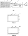
- FIG. 1 illustrates structural principles of a touch screen terminal having an NFC function according to an embodiment of the present invention. For ease of description, only portions related to the present invention are illustrated.
- the touch screen terminal comprises a touch screen 10, a touch control chip 20 and a terminal main controller 30.
- the touch screen 10 is an input device of a terminal device, and may be practiced by using a capacitive finger touch sensor screen and the like.
- the touch screen provide the functions of signal reception and transmission in the near field communication, and mainly comprises a touch sensing region 11 and a screen antenna 12.
- the touch sensing region 11 is deployed with a touch sensing electrode pattern, which is generally practiced by using an indium tin oxide (ITO) electrode pattern.
- ITO indium tin oxide
- the touch sensing electrode pattern is formed by several transparent conductive driving sensing lines in a strip shape or other shapes, and is configured to sense a touch operation by the finger.
- the screen antenna 12 is a single-turn conductive wire (for example, a silver paste or other conductive materials) deployed on a periphery of the touch screen.
- the conductive wire is originally used as a ground loop for ESD protection is used, and the ground loop is herein reused to implement both reception and transmission of near field communication signals and the ESD protections.
- the single-turn conductive wire is favorable to the design of a narrow frame.
- FIG. 2A illustrates a design structure of the touch screen 10 according to a first embodiment of the present invention.
- the screen antenna 12 is a contiguous annular line 121 arranged on a periphery of the touch sensing region 11, and has a line width of 0.1 mm to 2.0 mm and a thickness of 18 ⁇ m to 100 ⁇ m.
- the contiguous annular line 121 may form a direct current loop, and the impedance at the two ends thereof is less than 200 ohms.
- the electrode pattern of the touch sensing region 11 may be practiced by the conventional design.
- FIG. 2B is a design structure of the touch screen 10 according to a second embodiment of the present invention.
- the screen antenna 12 is an intermediately disconnected annular line 122 arranged on a periphery of the touch sensing region 11.
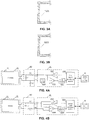
- a gap at the disconnection of the annular line 122 is of a straight line shape as illustrated in FIG. 3A .
- the straight line shape is easy to practice in engineering design, and has a lower requirement on the process precision than a bent line.
- the intermediate disconnection has a spacing of 0.5 to 2 mm.
- This structure is disadvantageous in that a slit is present in the middle part, and ESD protection fails to be provided for this part.
- the annular line 122 may also be a bent line shape as illustrated in FIG. 3B .
- the difficulty of such disconnected bent line is greater than the difficulty of the disconnected straight line in terms of practice and engineering design, and the requirement on the process precision is higher.
- the bent line has a spacing of 0.2 to 1 mm, and is advantageous in that no blind region in ESD protection exists.
- an alternating current impedance of the annular line 122 is the same as that in the first embodiment, which is less than 200 ohms, with the same line width of 0.1 to 2.0 mm and a thickness of 18 to 100 ⁇ m.
- the touch control chip 20 comprises a touch control manager 21 and a near field communication manager 22; wherein the touch control manager 21 is connected to the touch sensing electrode pattern, and configured to process a sensing signal from the touch control sensing electrode pattern and calculate a touch coordinate.
- the near field communication manager 22 is connected to two terminals of the screen antenna, and configured to process a near field communication transaction.
- the terminal main controller 30 is configured to process most of the transactions of the terminal, and is also configured to acquire and manage information of touch control and near field communication.
- FIG. 4A illustrates a structure of the near field communication manager 22 and connection of the near field communication manager 22 and a peripheral component according to the first embodiment of the present invention.
- the near field communication manager 22 comprises a reference voltage module 2211, a first reception buffering module 2221, a first sending module 2231, a first demodulation module 2241 and a first digital processing module 2251.
- a reference voltage output terminal of the reference voltage module 2211 is electrically connected to the screen antenna 12, and provides a reference voltage and a bias for an interior and an exterior of the touch control chip 20.
- the voltage of the reference voltage module may be half of the voltage of the power source or may be another voltage, for example, 1/3 to 2/3 of the voltage of the power source.
- An input terminal of the first reception buffering module 2221 is electrically connected to the screen antenna 12, and is mainly configured to buffer and amplify an external input signal. The signal is input via a single terminal.
- the input terminal of the first reception buffering module 2221 may also be electrically connected to the screen antenna 12 via a switch unit.
- the switch unit before the first reception buffering module 2221 is switched off, to prevent the first sending module 2231 from interfering a working bias state of the first reception buffering module 2221.
- the switch unit before the first reception buffering module 2221 is switched on, to facilitate reception and processing of the screen antenna signal.
- An output terminal of the first sending module 2231 is electrically connected to the screen antenna 12, and is configured to send out, via the screen antenna 12, a near field communication signal to be transmitted, which is a single-terminal output buffer having a specific driving capability and capable of outputting a modulated 13.56 MHz square wave.
- the first sending module 2231 may enter a high impedance state, to prevent the input signal from being bypassed, and ensure that the first reception buffering module 2221 is capable of working in a normal bias state.
- An input terminal of the first demodulation module 2241 is connected to the first reception buffering module 2221, and is configured to demodulate the signal coupled by the screen antenna (that is, the screen antenna 12) and then processed by the first reception buffering module 2221, thereby completing the task of demodulation from a radio frequency field to a digital signal.
- a first digital processing module 2251 with one terminal being connected to an output terminal of the first demodulation module 2241 and an input terminal of the first sending module 2231, and the other terminal being connected to the terminal main controller 30, is configured to decode the digital signal obtained via demodulation by the first demodulation module 2241, and send a decoding result to the terminal main controller 30.
- the first digital processing module 2251 is further configured to receive data to be sent from the terminal main controller 30 and demodulate the received data, and output a signal upon modulation to the first sending module 2231.
- the touch screen terminal further comprises a first filter module 401, wherein the screen antenna 12 is connected to the near field communication manager 22 via the first filter module 401.
- the first filter module 401 is configured to perform anti-electromagnetic interference (EMI) filter and impedance matching for a near field communication signal received and sent by the screen antenna 12, and comprises a first resistor R1, a first capacitor C1 and a second capacitor C2.
- EMI anti-electromagnetic interference
- One line terminal of the screen antenna 12 is electrically connected to the first reception buffering module 2221 and the first sending module 2231 via the first resistor R1, and the other line terminal of the screen antenna 12 is connected to the reference voltage output terminal of the reference voltage module 2221; the first capacitor C1 is connected between the two terminals of the screen antenna 12, and the second capacitor C2 is connected between the other line terminal of the screen antenna 12 and the ground.
- FIG. 4B illustrates a structure of the near field communication manager 22 and connection of the near field communication manager 22 and a peripheral component according to the second embodiment of the present invention.
- the near field communication manager 22 comprises a second reception buffering module 2222, a second sending module 2232, a second demodulation module 2242 and a second digital processing module 2252.
- the second reception buffering module 2222 is configured to buffer and amplify an external near field communication signal received by the screen antenna 12.
- the signal is input to the second reception buffering module 2222 in a differential manner, and the two input terminals of the second reception buffering module 2222 are respectively electrically connected to the two terminals of the screen antenna 12 via switch units.
- Two output terminals of the second sending module 2232 are respectively electrically connected to the two terminals, and the second sending module 2232 is configured to send out, via the screen antenna 12, a near field communication antenna to be output. During operation, the signals output by the two output terminals have opposite levels.
- the second sending module 2232 is an output buffer having a specific driving capability. When the second sending module 2232 is idle, the second sending module may enter a high impedance state, to prevent the input signal from being bypassed, and ensure that the second reception buffering module 2222 is capable of working in a normal bias state. The second sending module 2232 outputs signals in a differential manner.
- the switch unit before the second reception receiving module 2222 is switched off, to prevent the second sending module 2232 from interfering the working bias state of the second reception buffering module 2222; and when the second sending module 2232 is idle, the switch unit before the second reception buffering module 2222 is switched on, to facilitate reception and processing of the screen antenna signal.
- An input terminal of the second demodulation module 2242 is connected to the second reception buffering module 2222, and is configured to demodulate the signal amplified by the second reception buffering module 2222 into a digital signal, to complete the task of demodulation from a radio frequency field to a digital signal.
- a second digital processing module 2252 with one terminal being connected to an output terminal of the second demodulation module 2242 and an input terminal of the second sending module 2232, and the other terminal being connected to the terminal main controller 30, is configured to decode the digital signal obtained via demodulation by the second demodulation module 2242, and send a decoding result to the terminal main controller 30.
- the second digital processing module 2252 is further configured to receive data to be sent from the terminal main controller 30 and demodulate the received data, and output a signal upon modulation to the second sending module 2232.
- the touch screen terminal further comprises a second filter module 402, wherein the screen antenna 12 is connected to the near field communication manager 22 via the second filter module 402.
- the second filter module 402 is configured to perform EMI filter and impedance matching for a near field communication signal received and sent by the screen antenna 12, and comprises a second resistor R2, a third resistor R3 and a third capacitor C3.
- One line terminal of the screen antenna 12 is electrically connected to the second reception buffering module 2222 and the second sending module 2232 via the second resistor R2, and the other line terminal of the screen antenna 12 is connected to the second reception buffering module 2222 and the second sending module 2232 via the third resistor R3; the third capacitor C3 is connected between the two terminals of the screen antenna 12.
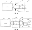
- an ESD protection function may be configured in the near field communication manager 22.
- the two manners are detailed as follows: in FIG. 5A , two ESD protective diodes 51 and 52 are respectively connected to the two terminals at the interface of the screen antenna and then connected to the ground line, thereby forming ESD protection and ensuring that the touch control chip circuit is more secure. Based on the touch control chip circuit, two devices are added, which thus increases the cost and occupy the circuit area. The advantage of this circuit lies in a better protection effect over that in FIG. 5B . As illustrated in FIG.
- two ESD protective circuits 231 and 232 are directly integrated in the touch control chip, to form ESD protection and ensure that the internal circuit of the chip is more secure.
- the ESD protective circuit 231 is connected between an output terminal of the second sending module 2232 and the ground
- the ESD protective circuit 232 is connected between the other output terminal of the second sending module 2232 and the ground.
- the ESD protective circuit achieves a very limited ESD protection effect and the cost of the chip is slightly increased.
- the advantage thereof lies in that the peripheral circuit is simple and the circuit area becomes smaller.
- the ESD protection function is configured in the interior or the exterior of the touch control chip 20. That is, when the ESD protection function is configured in the exterior of the chip, each of the two terminals of the screen antenna is connected to the ground via an ESD protective diode; and when the ESD protection function is configured in the interior of the chip, the reference voltage output terminals of the reference voltage module 2211 is connected to the ground via an ESD protective diode, and the output terminal of the first sending module 2231 is connected to the ground via another ESD protection diode.
- the signal since the conventional near field communication antenna is ideal, the signal does not need to be amplified. In addition, the signal is returned back to a card reader by means of regulating the power consumption load of the near field communication manager.
- the single-turn antenna according to the present invention has a great impedance and weak signal, and thus amplification is needed. If the signal needs to be returned back by means of regulating the load, after the display screen absorbs the energy, the returned signal is also very weak.
- the two problems that the wiring impedance of the single-turn silver paste is great and that the attenuation caused by the terminal display screen and the like elements to the communication signal is great, are solved by means of amplifying a signal and actively sending a driving signal by the reception buffering module in the circuitry.
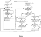
- FIG. 6 illustrates a working process of a touch screen terminal having the NFC function according to an embodiment of the present invention.
- the process mainly comprises touch control detection steps and near field communication detection steps.
- the touch control manager 21 detects whether a touch control operation is performed on the touch screen 10, and sends the calculated touch coordinate to the terminal main controller 30.
- the touch control manager 22 performs a full-screen detection and then starts performing the near field communication detection.
- Step 601 the main program of the touch control chip is started.
- Step 602 settings of the related register are initialized, for example, timer, I/O state and the like of the terminal main controller 30.
- Step 603 touch control detection is enabled; the related register and the related interrupt program are properly set, to enable the touch control detection process run automatically.
- Step 604 it is judged whether a full-screen scanning of touch control is completed; and if the full-screen scanning is not completed, a period of time later, it is continuously judged whether the full-screen scanning is completed.
- Step 605 if a full-screen touch control scanning is completed, coordinate information detected by the touch control is calculated based on the scanned data, and the coordinate information is reported to the terminal main controller 30.
- Step 606 the near field communication detection module is enabled after step 605, to receive a 13.56 MHz magnetic field signal from a card reader.
- Step 607 it is judged whether the 13.56 MHz magnetic field signal is received from the card reader; and if no such signal is received, the process directly returns to step 604, and a next run of touch control coordinate judgment is made.
- Step 608 if the 13.56 MHz magnetic field signal is received from the card reader, it is further judged whether the state set for the current RFID tag is a Type A (first state) or Type B (second state).
- the RFID tag comprises a near field communication manager and a screen antenna.
- the difference between Type A state and Type B state lies in that: the modulation signals corresponding to Type A have a 100% depth and are very strong, and reception and modulation of Type A signals are not easily subjected to the interference caused by the touch screen scanning signal, and thus the touch control detection does not need to be disabled; whereas the modulation signals corresponding to Type B signals have only a 10% depth, and reception and modulation of Type B signals are not easily subjected to the interference caused by the touch screen scanning signal, and thus the touch control detection needs to be disabled to eliminate the interference.
- Step 609 if the currently set state is Type A, the process enters Type A tag transaction service, for example, completion of a Type A process of ISO14443-3 and the like.
- Step 610 it is judged whether the current transaction is completed; and if not completed, the process goes to step 609 (in the case where the magnetic field of the card reader is not disabled and the command is not suspended).
- Step 611 if the current transaction is completed (in the case where the magnetic field of the card reader is disabled), the near field communication is disabled to save energy; and the process directly returns to step 604 to perform a next run of touch coordinate judgment.
- Step 612 if the currently set state is Type B, the touch control signal is firstly disabled to prevent the mutual interference between a touch control signal and a near field communication signal.
- Step 613 the process enters the Type B tag transaction service, for example, completion of a Type B process of ISO14443-3 and the like.
- Step 614 it is judged whether the current transaction is completed; and if not completed, the process goes to step 613 (in the case where the magnetic field of the card reader is not disabled and the command is not suspended).
- Step 615 if the current transaction is completed (in the case where the magnetic field of the card reader is disabled), the near field communication is disabled to save energy; and the process directly returns to step 603 and the touch control detection is enabled, to perform a next run of touch coordinate judgment.
- the terminal main controller 30 is responsible for perform operational processing for the data.
- the ESD conductive wire of the touch screen is reused as the antenna for near field communication, and compatibility of the touch detection with the near field communication function is achieved with almost zero cost. Since there is only one turn of screen antenna, the screen antenna may be simply practiced and suitable for the design of narrow frame screen. Since the screen antenna is deployed on the substrate of the touch screen, and does not need to be disassembled, problems such as abrasion may be prevented and thus smooth near field communication may be ensured.
- the present invention is mainly applicable to data exchange, financial transaction, access control management and the like scenarios.
Landscapes
- Engineering & Computer Science (AREA)
- General Engineering & Computer Science (AREA)
- Theoretical Computer Science (AREA)
- Computer Networks & Wireless Communication (AREA)
- Signal Processing (AREA)
- Human Computer Interaction (AREA)
- Physics & Mathematics (AREA)
- General Physics & Mathematics (AREA)
- Computer Hardware Design (AREA)
- Transceivers (AREA)
- Near-Field Transmission Systems (AREA)
Abstract
Description
- The present invention relates to the technical field of near field communication, and in particular, relates to an NFC antenna-integrated touch screen, a terminal and a near field communication method thereof.
- Near field communication (NFC) is a technology which implements non-contact identification and interconnection, which employs 13.56 MHz near field magnetic field communication mode and implements short-range wireless communication between mobile terminals or devices, consumable electronic products, PCs and smart control tools. This allows users to exchange information, and access contents and services simply and visually. Therefore, the NFC technology is an indispensable technology in the future electric products, and has a huge market potential.
- Currently, touch screens of most mobile phones are integrated with the NFC function. However, the antenna of the conventional NFC product is mainly disposed on a face of the battery or attached inside the shell. Generally, coils are formed by means of metal wiring on a PCB, and then the PCB or FPC having the coils is attached on the shell or the battery. The disadvantages lie in that the battery and the shell generally need to be repeatedly disassembled or assembled, such that the junction of the NFC antenna tends to be damaged or tends to be misaligned, which finally causing poor antenna signals and affecting use of the NFC function. In addition, the antenna of a NFC product is generally disposed inside the shell of the electronic product. If the shell is made from a metal material, the propagation of an NFC signal may be affected. Therefore, some limitations are caused to selection of materials of the shell of the electronic product.
- Accordingly, such deployment of the NFC antenna is not reasonable, and the junction thereof tends to be damaged or tends to be not aligned. As a result, antenna signals become poor, and selection of materials of the shell of the electronic product is subjected to limitations. To solve the technical problem, the Chinese patent application titled with NFC antenna-integrated touch screen, with the publication number
CN 102819346 A , discloses a touch screen integrated with an NFC antenna, wherein the NFC antenna is disposed on the touch screen and connected to a control board with a control chip, which integrating the touch control function and the NFC antenna function. Since the touch screen is a undetachable component in operation, during the use of an NFC antenna, problem such as poor signals, junction failures and the like , which might otherwise exist due to the interface abrasion and non-alignment, may be prevented, and this is also good for signal reception and transmission of the antenna, to ensure smooth communication. In addition, the touch screen integrated with the NFC antenna provides a solution for practice the scenario where the NFC signals are more conveniently received from the touch surface of the touch screen, or the NFC signal must be received from the touch surface of the touch screen. Furthermore, the electronic product equipped with the above touch screen transfers signals through the touch surface, thus it is not subjected to limitations caused by the NFC antenna when selecting materials of the shell. - Although the above patent application may prevent some of the problems of the electronic product integrated with the NFC function, other problems may also be caused. For example, the NFC antenna has multiple turns of coils fabricated by using the conductive wires in a wiring manner, which inevitably unfavorable to the process of the narrow frame screen.
- The technical problem to be solved by the present invention is to provide an NFC antenna-integrated touch screen, a terminal and a near field communication thereof. The touch screen terminal having the NFC function may ensure smooth communication, and is suitable for the process of a narrow frame screen.
- The present invention is practiced as follows: an NFC antenna-integrated touch screen, comprising a substrate, the substrate having a touch sensing region, a touch sensing electrode pattern being arranged in the touch sensing region; wherein a single-turn conductive wire is arranged on an outer side of the touch sensing region, the screen antenna being connected to an external near field communication manager as an antenna for near field communication.
- A touch screen terminal according to the present invention comprises an NFC antenna-integrated touch screen as defined above, and further comprises a touch control chip and a terminal main controller; wherein
the touch control chip comprises a touch control manager and a near field communication manager; wherein the touch control manager is connected to the touch sensing electrode pattern, and configured to process a sensing signal from the touch control sensing electrode pattern and calculate a touch coordinate; and the near field communication manager is connected to an screen antenna, and configured to process a near field communication transaction; and
the terminal main controller is configured to acquire and manage information of the touch control and near field communication. - A near field communication method of the touch screen terminal according to the present invention comprises the following steps:
- touch control detection: detecting, by a touch control manager, whether a touch control operation is performed on a touch screen, and send a calculated touch coordinate to a terminal main controller; and
- near field communication detection: after the touch control manager performs the screen detection, performing by a near field communication manager, near field communication detection.
- According to the present invention, the ESD conductive wire of the touch screen is reused as the antenna for near field communication, and compatibility of the touch detection with the near field communication function is achieved with almost zero cost. Since there is only one turn of screen antenna, the screen antenna may be simply practiced and suitable for the design of narrow frame screen. Since the screen antenna is deployed on the substrate of the touch screen, and does not need to be disassembled, problems such as abrasion may be prevented and thus smooth near field communication may be ensured.
-
-
FIG. 1 is a structural principle diagram of a touch screen terminal having an NFC function according to an embodiment of the present invention; -
FIG. 2A is a schematic design diagram of an NFC antenna-integrated touch screen according to a first embodiment of the present invention; -
FIG. 2B is a schematic design diagram of an NFC antenna-integrated touch screen according to a second embodiment of the present invention; -
FIG. 3A and FIG. 3B are two schematic diagrams of a gap shape of an annular line inFIG. 2B ; -
FIG. 4A is a schematic diagram of a structure of the near field communication manager and connection of the near field communication manager and a peripheral component according to the first embodiment of the present invention; -
FIG. 4B is a schematic diagram of a structure of a near field communication manager and connection of the near field communication manager and a peripheral component according to the second embodiment of the present invention; -
FIG. 5A and FIG. 5B are schematic structural diagrams of an added ESD protection function inFIG. 4B ; and -
FIG. 6 is a working flowchart of a touch screen terminal having an NFC function according to an embodiment of the present invention. - To make the objective, technical solution, and advantages of the present invention clearer, the following section describes the technical solutions of the present invention in combination with the accompanying drawings and embodiments. It should be understood that the embodiments described here are only exemplary ones for illustrating the present invention, and are not intended to limit the present invention.
- According to the present invention, an outermost layer of electrostatic discharge (ESD) conductive wire of a touch screen is modified to reuse this winding of ESD conductive wire as a near field communication antenna; in addition, a near field communication processing circuit, also referred to as a near field communication manager, is deployed in a touch control chip to implement combination of the touch control technology and the near field communication technology.
-
FIG. 1 illustrates structural principles of a touch screen terminal having an NFC function according to an embodiment of the present invention. For ease of description, only portions related to the present invention are illustrated. The touch screen terminal comprises atouch screen 10, atouch control chip 20 and a terminalmain controller 30. - The
touch screen 10 is an input device of a terminal device, and may be practiced by using a capacitive finger touch sensor screen and the like. In addition to sensing a touch operation performed by a finger, the touch screen provide the functions of signal reception and transmission in the near field communication, and mainly comprises atouch sensing region 11 and ascreen antenna 12. Thetouch sensing region 11 is deployed with a touch sensing electrode pattern, which is generally practiced by using an indium tin oxide (ITO) electrode pattern. The touch sensing electrode pattern is formed by several transparent conductive driving sensing lines in a strip shape or other shapes, and is configured to sense a touch operation by the finger. Thescreen antenna 12 is a single-turn conductive wire (for example, a silver paste or other conductive materials) deployed on a periphery of the touch screen. The conductive wire is originally used as a ground loop for ESD protection is used, and the ground loop is herein reused to implement both reception and transmission of near field communication signals and the ESD protections. In additions, the single-turn conductive wire is favorable to the design of a narrow frame. -
FIG. 2A illustrates a design structure of thetouch screen 10 according to a first embodiment of the present invention. In this embodiment, thescreen antenna 12 is a contiguousannular line 121 arranged on a periphery of thetouch sensing region 11, and has a line width of 0.1 mm to 2.0 mm and a thickness of 18 µm to 100 µm. The contiguousannular line 121 may form a direct current loop, and the impedance at the two ends thereof is less than 200 ohms. The electrode pattern of thetouch sensing region 11 may be practiced by the conventional design. -
FIG. 2B is a design structure of thetouch screen 10 according to a second embodiment of the present invention. In this embodiment, thescreen antenna 12 is an intermediately disconnectedannular line 122 arranged on a periphery of thetouch sensing region 11. A gap at the disconnection of theannular line 122 is of a straight line shape as illustrated inFIG. 3A . The straight line shape is easy to practice in engineering design, and has a lower requirement on the process precision than a bent line. The intermediate disconnection has a spacing of 0.5 to 2 mm. This structure is disadvantageous in that a slit is present in the middle part, and ESD protection fails to be provided for this part. In addition, theannular line 122 may also be a bent line shape as illustrated inFIG. 3B . The difficulty of such disconnected bent line is greater than the difficulty of the disconnected straight line in terms of practice and engineering design, and the requirement on the process precision is higher. The bent line has a spacing of 0.2 to 1 mm, and is advantageous in that no blind region in ESD protection exists. Although theannular line 122 is intermediately disconnected and no direct current loop is formed, an alternating current impedance of theannular line 122 is the same as that in the first embodiment, which is less than 200 ohms, with the same line width of 0.1 to 2.0 mm and a thickness of 18 to 100 µm. - Further referring to
FIG. 1 , thetouch control chip 20 comprises atouch control manager 21 and a nearfield communication manager 22; wherein thetouch control manager 21 is connected to the touch sensing electrode pattern, and configured to process a sensing signal from the touch control sensing electrode pattern and calculate a touch coordinate. The nearfield communication manager 22 is connected to two terminals of the screen antenna, and configured to process a near field communication transaction. The terminalmain controller 30 is configured to process most of the transactions of the terminal, and is also configured to acquire and manage information of touch control and near field communication. -
FIG. 4A illustrates a structure of the nearfield communication manager 22 and connection of the nearfield communication manager 22 and a peripheral component according to the first embodiment of the present invention. In this embodiment, the nearfield communication manager 22 comprises a reference voltage module 2211, a firstreception buffering module 2221, afirst sending module 2231, afirst demodulation module 2241 and a firstdigital processing module 2251. A reference voltage output terminal of the reference voltage module 2211 is electrically connected to thescreen antenna 12, and provides a reference voltage and a bias for an interior and an exterior of thetouch control chip 20. The voltage of the reference voltage module may be half of the voltage of the power source or may be another voltage, for example, 1/3 to 2/3 of the voltage of the power source. An input terminal of the firstreception buffering module 2221 is electrically connected to thescreen antenna 12, and is mainly configured to buffer and amplify an external input signal. The signal is input via a single terminal. The input terminal of the firstreception buffering module 2221 may also be electrically connected to thescreen antenna 12 via a switch unit. When the sendingmodule 2231 works, the switch unit before the firstreception buffering module 2221 is switched off, to prevent thefirst sending module 2231 from interfering a working bias state of the firstreception buffering module 2221. When thefirst sending module 2231 is idle, the switch unit before the firstreception buffering module 2221 is switched on, to facilitate reception and processing of the screen antenna signal. An output terminal of thefirst sending module 2231 is electrically connected to thescreen antenna 12, and is configured to send out, via thescreen antenna 12, a near field communication signal to be transmitted, which is a single-terminal output buffer having a specific driving capability and capable of outputting a modulated 13.56 MHz square wave. When thefirst sending module 2231 is idle, the first sending module may enter a high impedance state, to prevent the input signal from being bypassed, and ensure that the firstreception buffering module 2221 is capable of working in a normal bias state. An input terminal of thefirst demodulation module 2241 is connected to the firstreception buffering module 2221, and is configured to demodulate the signal coupled by the screen antenna (that is, the screen antenna 12) and then processed by the firstreception buffering module 2221, thereby completing the task of demodulation from a radio frequency field to a digital signal. A firstdigital processing module 2251, with one terminal being connected to an output terminal of thefirst demodulation module 2241 and an input terminal of thefirst sending module 2231, and the other terminal being connected to the terminalmain controller 30, is configured to decode the digital signal obtained via demodulation by thefirst demodulation module 2241, and send a decoding result to the terminalmain controller 30. Moreover, the firstdigital processing module 2251 is further configured to receive data to be sent from the terminalmain controller 30 and demodulate the received data, and output a signal upon modulation to thefirst sending module 2231. - Further, in this embodiment, the touch screen terminal further comprises a
first filter module 401, wherein thescreen antenna 12 is connected to the nearfield communication manager 22 via thefirst filter module 401. Thefirst filter module 401 is configured to perform anti-electromagnetic interference (EMI) filter and impedance matching for a near field communication signal received and sent by thescreen antenna 12, and comprises a first resistor R1, a first capacitor C1 and a second capacitor C2. One line terminal of thescreen antenna 12 is electrically connected to the firstreception buffering module 2221 and thefirst sending module 2231 via the first resistor R1, and the other line terminal of thescreen antenna 12 is connected to the reference voltage output terminal of thereference voltage module 2221; the first capacitor C1 is connected between the two terminals of thescreen antenna 12, and the second capacitor C2 is connected between the other line terminal of thescreen antenna 12 and the ground. -
FIG. 4B illustrates a structure of the nearfield communication manager 22 and connection of the nearfield communication manager 22 and a peripheral component according to the second embodiment of the present invention. In this embodiment, the nearfield communication manager 22 comprises a secondreception buffering module 2222, asecond sending module 2232, asecond demodulation module 2242 and a seconddigital processing module 2252. The secondreception buffering module 2222 is configured to buffer and amplify an external near field communication signal received by thescreen antenna 12. The signal is input to the secondreception buffering module 2222 in a differential manner, and the two input terminals of the secondreception buffering module 2222 are respectively electrically connected to the two terminals of thescreen antenna 12 via switch units. Two output terminals of thesecond sending module 2232 are respectively electrically connected to the two terminals, and thesecond sending module 2232 is configured to send out, via thescreen antenna 12, a near field communication antenna to be output. During operation, the signals output by the two output terminals have opposite levels. To be specific, thesecond sending module 2232 is an output buffer having a specific driving capability. When thesecond sending module 2232 is idle, the second sending module may enter a high impedance state, to prevent the input signal from being bypassed, and ensure that the secondreception buffering module 2222 is capable of working in a normal bias state. Thesecond sending module 2232 outputs signals in a differential manner. To be specific, when a signal is output, if one terminal of thesecond sending module 2232 is a high level, the other terminal is a low level; when thesecond sending module 2232 is idle, the two terminals thereof both output high impedance. When thesecond sending module 2232 is idle, the switch unit before the secondreception receiving module 2222 is switched off, to prevent thesecond sending module 2232 from interfering the working bias state of the secondreception buffering module 2222; and when thesecond sending module 2232 is idle, the switch unit before the secondreception buffering module 2222 is switched on, to facilitate reception and processing of the screen antenna signal. - An input terminal of the
second demodulation module 2242 is connected to the secondreception buffering module 2222, and is configured to demodulate the signal amplified by the secondreception buffering module 2222 into a digital signal, to complete the task of demodulation from a radio frequency field to a digital signal. A seconddigital processing module 2252, with one terminal being connected to an output terminal of thesecond demodulation module 2242 and an input terminal of thesecond sending module 2232, and the other terminal being connected to the terminalmain controller 30, is configured to decode the digital signal obtained via demodulation by thesecond demodulation module 2242, and send a decoding result to the terminalmain controller 30. Moreover, the seconddigital processing module 2252 is further configured to receive data to be sent from the terminalmain controller 30 and demodulate the received data, and output a signal upon modulation to thesecond sending module 2232. - Further, in this embodiment, the touch screen terminal further comprises a
second filter module 402, wherein thescreen antenna 12 is connected to the nearfield communication manager 22 via thesecond filter module 402. Thesecond filter module 402 is configured to perform EMI filter and impedance matching for a near field communication signal received and sent by thescreen antenna 12, and comprises a second resistor R2, a third resistor R3 and a third capacitor C3. One line terminal of thescreen antenna 12 is electrically connected to the secondreception buffering module 2222 and thesecond sending module 2232 via the second resistor R2, and the other line terminal of thescreen antenna 12 is connected to the secondreception buffering module 2222 and thesecond sending module 2232 via the third resistor R3; the third capacitor C3 is connected between the two terminals of thescreen antenna 12. - Further, as illustrated in
FIG. 4B , an ESD protection function may be configured in the nearfield communication manager 22. As illustrated inFIG. 5A and FIG. 5B , the two manners are detailed as follows: inFIG. 5A , two ESDprotective diodes 51 and 52 are respectively connected to the two terminals at the interface of the screen antenna and then connected to the ground line, thereby forming ESD protection and ensuring that the touch control chip circuit is more secure. Based on the touch control chip circuit, two devices are added, which thus increases the cost and occupy the circuit area. The advantage of this circuit lies in a better protection effect over that inFIG. 5B . As illustrated inFIG. 5B , two ESDprotective circuits protective circuit 231 is connected between an output terminal of thesecond sending module 2232 and the ground, and the ESDprotective circuit 232 is connected between the other output terminal of thesecond sending module 2232 and the ground. The ESD protective circuit achieves a very limited ESD protection effect and the cost of the chip is slightly increased. The advantage thereof lies in that the peripheral circuit is simple and the circuit area becomes smaller. - As illustrated in
FIG. 4A , similarly, the ESD protection function is configured in the interior or the exterior of thetouch control chip 20. That is, when the ESD protection function is configured in the exterior of the chip, each of the two terminals of the screen antenna is connected to the ground via an ESD protective diode; and when the ESD protection function is configured in the interior of the chip, the reference voltage output terminals of the reference voltage module 2211 is connected to the ground via an ESD protective diode, and the output terminal of thefirst sending module 2231 is connected to the ground via another ESD protection diode. - Referring to the structures of the near field communication manager as illustrated in
FIG. 4A and FIG. 4B , since the conventional near field communication antenna is ideal, the signal does not need to be amplified. In addition, the signal is returned back to a card reader by means of regulating the power consumption load of the near field communication manager. However, the single-turn antenna according to the present invention has a great impedance and weak signal, and thus amplification is needed. If the signal needs to be returned back by means of regulating the load, after the display screen absorbs the energy, the returned signal is also very weak. Therefore, the two problems that the wiring impedance of the single-turn silver paste is great and that the attenuation caused by the terminal display screen and the like elements to the communication signal is great, are solved by means of amplifying a signal and actively sending a driving signal by the reception buffering module in the circuitry. -
FIG. 6 illustrates a working process of a touch screen terminal having the NFC function according to an embodiment of the present invention. The process mainly comprises touch control detection steps and near field communication detection steps. In the touch control detection steps, thetouch control manager 21 detects whether a touch control operation is performed on thetouch screen 10, and sends the calculated touch coordinate to the terminalmain controller 30. In the near field communication detection steps, thetouch control manager 22 performs a full-screen detection and then starts performing the near field communication detection. - Step 601: the main program of the touch control chip is started.
- Step 602: settings of the related register are initialized, for example, timer, I/O state and the like of the terminal
main controller 30. - Step 603: touch control detection is enabled; the related register and the related interrupt program are properly set, to enable the touch control detection process run automatically.
- Step 604: it is judged whether a full-screen scanning of touch control is completed; and if the full-screen scanning is not completed, a period of time later, it is continuously judged whether the full-screen scanning is completed.
- Step 605: if a full-screen touch control scanning is completed, coordinate information detected by the touch control is calculated based on the scanned data, and the coordinate information is reported to the terminal
main controller 30. - Step 606: the near field communication detection module is enabled after
step 605, to receive a 13.56 MHz magnetic field signal from a card reader. - Step 607: it is judged whether the 13.56 MHz magnetic field signal is received from the card reader; and if no such signal is received, the process directly returns to step 604, and a next run of touch control coordinate judgment is made.
- Step 608: if the 13.56 MHz magnetic field signal is received from the card reader, it is further judged whether the state set for the current RFID tag is a Type A (first state) or Type B (second state). The RFID tag comprises a near field communication manager and a screen antenna. In the embodiment of the present invention, the difference between Type A state and Type B state lies in that: the modulation signals corresponding to Type A have a 100% depth and are very strong, and reception and modulation of Type A signals are not easily subjected to the interference caused by the touch screen scanning signal, and thus the touch control detection does not need to be disabled; whereas the modulation signals corresponding to Type B signals have only a 10% depth, and reception and modulation of Type B signals are not easily subjected to the interference caused by the touch screen scanning signal, and thus the touch control detection needs to be disabled to eliminate the interference.
- Step 609: if the currently set state is Type A, the process enters Type A tag transaction service, for example, completion of a Type A process of ISO14443-3 and the like.
- Step 610: it is judged whether the current transaction is completed; and if not completed, the process goes to step 609 (in the case where the magnetic field of the card reader is not disabled and the command is not suspended).
- Step 611: if the current transaction is completed (in the case where the magnetic field of the card reader is disabled), the near field communication is disabled to save energy; and the process directly returns to step 604 to perform a next run of touch coordinate judgment.
- Step 612: if the currently set state is Type B, the touch control signal is firstly disabled to prevent the mutual interference between a touch control signal and a near field communication signal.
- Step 613: the process enters the Type B tag transaction service, for example, completion of a Type B process of ISO14443-3 and the like.
- Step 614: it is judged whether the current transaction is completed; and if not completed, the process goes to step 613 (in the case where the magnetic field of the card reader is not disabled and the command is not suspended).
- Step 615: if the current transaction is completed (in the case where the magnetic field of the card reader is disabled), the near field communication is disabled to save energy; and the process directly returns to step 603 and the touch control detection is enabled, to perform a next run of touch coordinate judgment.
- After two functions are enabled, if not disabled, the two functions run parallelly and data is generated in a space of a register. The terminal
main controller 30 is responsible for perform operational processing for the data. - In conclusion, according to the present invention, the ESD conductive wire of the touch screen is reused as the antenna for near field communication, and compatibility of the touch detection with the near field communication function is achieved with almost zero cost. Since there is only one turn of screen antenna, the screen antenna may be simply practiced and suitable for the design of narrow frame screen. Since the screen antenna is deployed on the substrate of the touch screen, and does not need to be disassembled, problems such as abrasion may be prevented and thus smooth near field communication may be ensured. In addition, the two problems that the wiring impedance of the single-turn silver slurry is great and that the attenuation caused by the terminal display screen and the like elements to the communication signal is great are solved by means of amplifying a signal and actively sending a driving signal by the reception buffering module. The present invention is mainly applicable to data exchange, financial transaction, access control management and the like scenarios.
- Described above are merely preferred embodiments of the present invention, but are not intended to limit the present invention. Any modification, equivalent replacement, or improvement made without departing from the spirit and principle of the present invention should fall within the protection scope of the present invention.
Claims (20)
- An NFC antenna-integrated touch screen,
a substrate having a touch sensing region;a touch sensing electrode arranged in the touch sensing region; anda single-turn conductive wire arranged on a periphery of the touch sensing region, wherein the single-turn conductive wire forms a screen antenna for near field communication, and the screen antenna is connected to an external near field communication manage. - The touch screen according to claim 1, wherein the screen antenna is a contiguous annular line surrounding the periphery of the touch sensing region, and two terminals of the screen antenna are connected to the external near field communication manager.
- The touch screen according to claim 1, wherein the screen antenna is an intermediately disconnected annular line surrounding the periphery of the touch sensing region, a gap at the disconnection being of a straight line shape or a bent line shape, and two terminals of the screen antenna are connected to the external near field communication manager.
- The touch screen according to claim 2 or 3, wherein the screen antenna has a line width of 0.1 to 2.0 mm, a thickness of 18 to 100 µm and an impedance of less than 200 ohms.
- A touch screen terminal, comprising an NFC antenna-integrated touch screen as defined in any one of claims 1 to 4, and further comprising a touch control chip and a terminal main controller; wherein
the touch control chip comprises a touch control manager and a near field communication manager; wherein the touch control manager is connected to the touch sensing electrode pattern, and configured to process a sensing signal from the touch control sensing electrode pattern and calculate a touch coordinate; and the near field communication manager is connected to a screen antenna, and configured to process a near field communication transaction; and
a terminal main controller configured to acquire and manage information of the touch control and near field communication. - The touch screen terminal according to claim 5, wherein the near field communication manager comprises:a reference voltage module with a reference voltage output terminal thereof being electrically connected to the screen antenna, which the reference voltage module is configured to provide a reference voltage and a bias for an interior and an exterior of the touch control chip;a first reception buffering module with an input terminal thereof being electrically connected to the screen antenna, the first reception buffering module is configured to buffer and amplify an external near field communication signal received by the screen antenna;a first sending module with an output terminal being electrically connected to the screen antenna, the first sending module is configured to sent out, via the screen antenna, a near field communication signal to be output ;a first demodulation module with an input terminal thereof being electrically connected to the first reception buffering module, the first demodulation module is configured to demodulate the signal amplified by the first reception buffering module into a digital signal; anda first digital processing module with one terminal being connected to an output terminal of the first demodulation module and an input terminal of the first sending module, and the other terminal being connected to the terminal main controller, the first digital processing module is configured to decode the digital signal obtained via demodulation by the first demodulation module, and send a decoding result to the terminal main controller; and is further configured to receive data to be sent from the terminal main controller and demodulate the received data, and output a signal upon modulation to the first sending module.
- The touch screen terminal according to claim 6, wherein the first reception buffering module and the first sending module work at different time.
- The touch screen terminal according to claim 7, wherein the input terminal of the first reception buffering module is electrically connected to the screen antenna via a switch unit; when the first reception buffering module works, the switch unit is switched on; and when the first sending module works, the switch unit is switched off.
- The touch screen terminal according to claim 7 or 8, wherein if the first sending module is idle, the output terminal thereof stays in a high-impedance state.
- The touch screen terminal according to any one of claims 6 to 8, wherein the touch screen terminal further comprises a first filter module, and the screen antenna is connected to the near field communication manager via the first filter module;
wherein the first filter module is configured to perform anti-electromagnetic interference filter and/or impedance matching for a near field communication signal received and sent by the screen antenna, and the first filter module comprises a first resistor, a first capacitor and a second capacitor, wherein one terminal of the screen antenna is electrically connected to the first reception buffering module and the first sending module via the first resistor, and the other terminal of the screen antenna is connected to the reference voltage output terminal of the reference voltage module, the first capacitor is connected between the two terminals of the screen antenna, and the second capacitor is connected between the other line terminal of the screen antenna and the ground. - The touch screen terminal according to claim 5, wherein the near field communication manager comprises:a second reception buffering module with two input terminals thereof being respectively electrically connected two terminals of the screen antenna, the second reception buffering module is configured to buffer and amplify an external near field communication signal received by the screen antenna;a second sending module with two output terminals thereof being respectively electrically connected to two terminals of the screen antenna, the second sending module is configured to send out, via the screen antenna, a near field communication signal to be output, and during working, the two output terminals outputting signals with opposite levels;a second demodulation module with an input terminal thereof being electrically connected to the second reception buffering module, the second demodulation module is configured to demodulate the signal amplified by the second reception buffering nodule into a digital signal; anda second digital processing module with one terminal being connected to an output terminal of the second demodulation module and an input terminal of the second sending module, and the other terminal being connected to the terminal main controller, the second digital processing module is configured to decode the digital signal obtained via demodulation by the second demodulation module, and send a decoding result to the terminal main controller; and is further configured to receive data to be sent from the terminal main controller and demodulate the received data, and output a signal upon modulation to the second sending module.
- The touch screen terminal according to claim 11, wherein the second reception buffering module and the second sending module work at different time.
- The touch screen terminal according to claim 12, wherein the two input terminals of the second reception buffering module are respectively electrically connected to the screen antenna via a switch unit; when the second reception buffering module works, the switch unit is switched on; and when the sending module works, the switch unit is switched off.
- The touch screen terminal according to claim 12 or 13, wherein when the second sending module is idle, the two output terminals thereof both stay in a high-impedance state.
- The touch screen terminal according to any one of claims 11 to 13, wherein the touch screen terminal further comprises a second filter module, and the screen antenna is connected to the near field communication manager via the second filter module;
wherein the second filter module is configured to perform anti-electromagnetic interference filter and impedance matching for a near field communication signal received and sent by the screen antenna, and the second filter module comprises a second resistor, a third resistor and a third capacitor, wherein one line terminal of the screen antenna is electrically connected to the second reception buffering module and the second sending module via the second resistor and the other line terminal of the screen antenna is connected to the second reception buffering module and the second sending module via the third resistor, and the third capacitor is connected between the two terminals of the screen antenna. - The touch screen terminal according to claim 5, wherein each of the two terminals of the screen antenna is respectively connected to the ground via an ESD protective diode.
- The touch screen terminal according to claim 10, wherein the reference voltage output terminal of the reference voltage module is connected to the ground via an ESD protective diode, and the output terminal of the first sending module is connected to the ground via another ESD protective diode.
- The touch screen terminal according to claim 15, wherein each of the two terminals of the second sending module is respectively connected to the ground via an ESD protective diode.
- A near field communication method for a touch screen terminal as defined in any one of claims 5 to 18, comprising the following steps:detecting, by a touch control manager, whether a touch control operation is performed on a touch screen, and send a calculated touch coordinate to a terminal main controller; andperforming, by a near field communication manager, a near field communication detection after the detecting by the touch control manager.
- The near field communication method according to claim 19, wherein the performing the near field communication detection comprises:detecting whether a signal from a card reader is received, if no signal is received, performing the detecting by the touch control manager, and if a signal is detected, judging whether an RFID tag works in a first state or a second state, wherein the RFID tag comprises the near field communication manager and a screen antenna;processing a tag transaction service in the first state when it is judged that the RFID tag works in the first state;disabling the touch control manager and processing a tag transaction service in the second state when it is judged that the RFID tag works in the second state; and disabling the near field communication manager upon completion of processing the tag transaction service.
Applications Claiming Priority (2)
| Application Number | Priority Date | Filing Date | Title |
|---|---|---|---|
| CN201410746166.8A CN104485983B (en) | 2014-12-09 | 2014-12-09 | Touch-screen, terminal and its near field communication method of integrated NFC antenna |
| PCT/CN2015/072822 WO2016090753A1 (en) | 2014-12-09 | 2015-02-12 | Touch screen integrated with nfc antenna, terminal, and near field communication method therefor |
Publications (3)
| Publication Number | Publication Date |
|---|---|
| EP3232580A1 true EP3232580A1 (en) | 2017-10-18 |
| EP3232580A4 EP3232580A4 (en) | 2018-08-15 |
| EP3232580B1 EP3232580B1 (en) | 2020-12-30 |
Family
ID=52760499
Family Applications (1)
| Application Number | Title | Priority Date | Filing Date |
|---|---|---|---|
| EP15866742.8A Active EP3232580B1 (en) | 2014-12-09 | 2015-02-12 | Touch screen integrated with nfc antenna, terminal, and near field communication method therefor |
Country Status (5)
| Country | Link |
|---|---|
| US (1) | US10396430B2 (en) |
| EP (1) | EP3232580B1 (en) |
| KR (1) | KR102056517B1 (en) |
| CN (1) | CN104485983B (en) |
| WO (1) | WO2016090753A1 (en) |
Families Citing this family (36)
| Publication number | Priority date | Publication date | Assignee | Title |
|---|---|---|---|---|
| US9952732B2 (en) | 2014-12-10 | 2018-04-24 | Pixart Imaging Inc. | Capacitive touch device, capacitive communication device and communication system |
| US10551949B2 (en) | 2015-05-08 | 2020-02-04 | Intel Corporation | Display integrated antenna |
| US20180092136A1 (en) * | 2015-05-15 | 2018-03-29 | Sharp Kabushiki Kaisha | Information processing device, method for controlling information processing device, and control device |
| CN105162969A (en) * | 2015-08-10 | 2015-12-16 | 京东方科技集团股份有限公司 | Display device, mobile equipment and display method |
| CN105224136B (en) * | 2015-10-13 | 2018-02-23 | 京东方科技集团股份有限公司 | A kind of touch-control display panel and preparation method thereof, driving method, display device |
| CN106598316A (en) * | 2015-10-19 | 2017-04-26 | 上海蓝沛信泰光电科技有限公司 | Thin film integrating touch handwriting sensor and near field communication antenna and preparation method thereof |
| KR102406686B1 (en) * | 2015-11-10 | 2022-06-08 | 삼성전자주식회사 | Antenna device and electronic device with the same |
| CN105446526A (en) * | 2015-11-16 | 2016-03-30 | 业成光电(深圳)有限公司 | Touch panel, short-range wireless communications technology terminal, and production method thereof |
| JP6292288B1 (en) * | 2016-12-09 | 2018-03-14 | ダイキン工業株式会社 | Remote controller |
| CN106850959B (en) * | 2016-12-22 | 2019-10-25 | 努比亚技术有限公司 | A kind of terminal, antenna member control device and method |
| DE102017130379A1 (en) * | 2017-03-30 | 2018-10-04 | Huf Hülsbeck & Fürst Gmbh & Co. Kg | Sensor device with capacitive sensor for motor vehicles |
| CN109213356B (en) * | 2017-07-06 | 2022-02-11 | 上海商米科技集团股份有限公司 | Control method of intelligent terminal and intelligent terminal |
| CN109496395A (en) * | 2018-09-28 | 2019-03-19 | 深圳市汇顶科技股份有限公司 | A circuit and electronic equipment |
| CN109884876A (en) * | 2019-03-04 | 2019-06-14 | 出门问问信息科技有限公司 | Smartwatch |
| CN109885215B (en) * | 2019-04-04 | 2024-11-12 | 苏州智博信息科技有限公司 | A capacitive touch screen with shielding effectiveness |
| CN109884828B (en) * | 2019-04-17 | 2022-01-11 | 京东方科技集团股份有限公司 | Display panel and mobile terminal |
| CN110442250B (en) * | 2019-06-28 | 2021-06-01 | 华为技术有限公司 | Touch pad with NFC function and terminal equipment |
| CN110729550B (en) * | 2019-09-02 | 2021-11-19 | 深圳市飞亚达精密科技有限公司 | Antenna device and intelligent watch |
| US11762624B2 (en) * | 2019-09-23 | 2023-09-19 | Sonos, Inc. | Capacitive touch sensor with integrated antenna(s) for playback devices |
| CN110716664A (en) * | 2019-09-29 | 2020-01-21 | 维沃移动通信有限公司 | Touch screen and electronic equipment |
| CN113220149B (en) | 2020-01-20 | 2024-06-28 | 华为技术有限公司 | Touch module and terminal equipment |
| CN113675582A (en) * | 2020-05-15 | 2021-11-19 | 威速达(苏州)电子有限公司昆山分公司 | Touch Component with Near Field Communication Circuit |
| CN111949155A (en) * | 2020-06-28 | 2020-11-17 | 盈天实业(深圳)有限公司 | Touch substrate and preparation method, touch module, touch display screen, electronic equipment |
| CN111800528B (en) * | 2020-06-30 | 2021-11-16 | 上海摩勤智能技术有限公司 | Terminal device |
| CN111754659A (en) * | 2020-07-06 | 2020-10-09 | 北京智芯微电子科技有限公司 | Security smart lock based on NFC energy acquisition |
| KR102371033B1 (en) | 2020-07-22 | 2022-03-04 | 동우 화인켐 주식회사 | Antenna-inserted electrode structure and image display device including the same |
| CN112051936B (en) * | 2020-08-21 | 2024-05-28 | 维信诺科技股份有限公司 | Display device |
| CN112468620B (en) * | 2020-11-25 | 2023-06-27 | Oppo广东移动通信有限公司 | Antenna communication control method and device, terminal equipment and storage medium |
| CN112993554B (en) * | 2021-02-19 | 2023-04-14 | 维沃移动通信有限公司 | Electronic equipment |
| CN115701316B (en) * | 2021-05-31 | 2026-06-12 | 京东方科技集团股份有限公司 | Display substrate and its manufacturing method, display module, display device |
| CN113900611A (en) * | 2021-10-08 | 2022-01-07 | 泰安北航科技园信息科技有限公司 | A five-screen |
| CN115220587B (en) * | 2022-07-27 | 2026-03-20 | 深圳市汇顶科技股份有限公司 | Touchpad and electronic devices |
| US12368470B2 (en) | 2023-04-17 | 2025-07-22 | Ford Global Technologies, Llc | Placement of mobile wireless device on a display panel with a hidden antenna |
| CN116306725B (en) * | 2023-05-23 | 2023-09-15 | 深圳贝特莱电子科技股份有限公司 | Double-layer touch pad and NFC function control method thereof |
| WO2025184270A1 (en) * | 2024-02-29 | 2025-09-04 | Microchip Touch Solutions Limited | Touch controller with integrated rfid read capabilities, including related systems, apparatuses, and methods |
| CN118521303B (en) * | 2024-07-24 | 2024-12-20 | 支付宝(杭州)信息技术有限公司 | Payment terminal and payment method based on near field communication |
Family Cites Families (38)
| Publication number | Priority date | Publication date | Assignee | Title |
|---|---|---|---|---|
| CN1457530A (en) * | 2001-03-02 | 2003-11-19 | 摩托罗拉公司 | Parasitic antenna element and wireless communication device incorporating the same |
| WO2006088431A1 (en) * | 2005-02-18 | 2006-08-24 | Agency For Science, Technology And Research | Architecture for rfid tag reader/writer |
| GB0623653D0 (en) * | 2006-11-27 | 2007-01-03 | Innovision Res & Tech Plc | Near field RF communicators and near field RF communications enabled devices |
| WO2010070401A1 (en) * | 2008-12-21 | 2010-06-24 | Laird Technologies Ab | Antenna assemblies for use with portable communications devices |
| US8339372B2 (en) * | 2009-04-20 | 2012-12-25 | Broadcom Corporation | Inductive touch screen with integrated antenna for use in a communication device and methods for use therewith |
| US8466839B2 (en) * | 2009-07-17 | 2013-06-18 | Apple Inc. | Electronic devices with parasitic antenna resonating elements that reduce near field radiation |
| US8256539B2 (en) * | 2009-07-30 | 2012-09-04 | Louisiana Tech University Research Foundation | Steerable ground piercing tools |
| KR101031414B1 (en) * | 2009-11-25 | 2011-04-26 | 주식회사 하이닉스반도체 | RFID device |
| KR101068308B1 (en) * | 2009-12-23 | 2011-09-28 | 주식회사 하이닉스반도체 | RFID device |
| EP2532098A4 (en) * | 2010-02-02 | 2015-12-16 | Nokia Technologies Oy | APPARATUS |
| US8725088B2 (en) * | 2010-04-05 | 2014-05-13 | Texas Instruments Incorporated | Antenna solution for near-field and far-field communication in wireless devices |
| US8605816B2 (en) * | 2010-05-27 | 2013-12-10 | Sony Corporation | Non-contact wireless communication apparatus, method of waveform-shaping envelope curve, and mobile electronic device |
| TW201222964A (en) * | 2010-11-30 | 2012-06-01 | Inventec Corp | An antenna structure |
| US9071955B2 (en) * | 2010-11-30 | 2015-06-30 | Panasonic Intellectual Property Corporation Of America | Communication device and communication method |
| KR20120063652A (en) | 2010-12-08 | 2012-06-18 | 삼성전자주식회사 | Antenna device for potable terminal |
| CN102111169A (en) * | 2011-03-14 | 2011-06-29 | 中兴通讯股份有限公司 | Double-mode mobile terminal |
| US20120329524A1 (en) * | 2011-06-22 | 2012-12-27 | Kent Joel C | Touch sensor and antenna integration along an electronic device housing |
| JP6105572B2 (en) * | 2011-07-07 | 2017-03-29 | サーク・コーポレーション | Induced current cancellation in touch sensing devices with built-in near field communication antennas |
| KR101806945B1 (en) * | 2011-07-13 | 2017-12-11 | 삼성전자주식회사 | Near field communication antenna device of a mobile terminal |
| US8681460B2 (en) * | 2011-07-13 | 2014-03-25 | Sony Corporation | Electrostatic discharge (ESD) protection device |
| JP5598611B2 (en) * | 2011-10-26 | 2014-10-01 | 株式会社村田製作所 | Variable capacitance element and high frequency device |
| CN102509866A (en) * | 2011-11-03 | 2012-06-20 | 上海坤锐电子科技有限公司 | SIM antenna capable of balancing communication distance in mobile payment transfer bridge scheme |
| US8718553B2 (en) * | 2012-01-27 | 2014-05-06 | Blackberry Limited | Communications device and method for having integrated NFC antenna and touch screen display |
| EP2620845B1 (en) * | 2012-01-27 | 2018-08-22 | BlackBerry Limited | Communications device for having integrated NFC antenna and touch screen display |
| US8922527B2 (en) * | 2012-02-15 | 2014-12-30 | Cypress Semiconductor Corporation | Multi-purpose stylus antenna |
| CN102819346B (en) * | 2012-04-06 | 2016-01-13 | 信利工业(汕尾)有限公司 | A kind of touch-screen of integrated NFC antenna |
| US20130293354A1 (en) * | 2012-05-01 | 2013-11-07 | Jeevan Kumar Vemagiri | Discontinuous loop antennas suitable for radio-frequency identification (rfid) tags, and related components, systems, and methods |
| TWI505553B (en) * | 2012-06-21 | 2015-10-21 | Wistron Neweb Corp | Multi-function radio-frequency device, computer system and method of operating multi-function radio-frequency device |
| CN103904412A (en) * | 2012-12-26 | 2014-07-02 | 鸿富锦精密工业(深圳)有限公司 | Portable electronic device with NFC antenna |
| TWI562556B (en) * | 2012-12-26 | 2016-12-11 | Hon Hai Prec Ind Co Ltd | Portable electronic device having nfc antenna |
| CN103904411A (en) * | 2012-12-26 | 2014-07-02 | 鸿富锦精密工业(深圳)有限公司 | Portable electronic device with NFC antenna |
| US8934837B2 (en) * | 2013-01-03 | 2015-01-13 | Blackberry Limited | Mobile wireless communications device including NFC antenna matching control circuit and associated methods |
| CN104124997B (en) * | 2013-04-29 | 2016-04-27 | 联发科技(新加坡)私人有限公司 | Control method and the device of the modulation index of near-field communication equipment |
| CN103259569B (en) * | 2013-05-14 | 2015-04-22 | 深圳市汇顶科技股份有限公司 | Touch terminals and near-field communication method and system thereof |
| CN103944614B (en) * | 2014-03-21 | 2017-01-11 | 深圳市汇顶科技股份有限公司 | Near field communication system and terminals |
| US10033435B2 (en) * | 2014-06-26 | 2018-07-24 | Intel IP Corporation | Apparatus, system and method of detecting an activity of a wireless communication device |
| CN104090680B (en) * | 2014-07-23 | 2017-07-25 | 上海天马微电子有限公司 | Touch panel, driving method thereof and electronic equipment |
| KR102443842B1 (en) * | 2015-09-14 | 2022-09-16 | 삼성전자주식회사 | Tag detector of NFC device, NFC device and mobile device including the NFC device |
-
2014
- 2014-12-09 CN CN201410746166.8A patent/CN104485983B/en active Active
-
2015
- 2015-02-12 EP EP15866742.8A patent/EP3232580B1/en active Active
- 2015-02-12 WO PCT/CN2015/072822 patent/WO2016090753A1/en not_active Ceased
- 2015-02-12 KR KR1020167022334A patent/KR102056517B1/en active Active
-
2016
- 2016-08-26 US US15/248,695 patent/US10396430B2/en active Active
Also Published As
| Publication number | Publication date |
|---|---|
| KR102056517B1 (en) | 2019-12-16 |
| CN104485983A (en) | 2015-04-01 |
| US20160365620A1 (en) | 2016-12-15 |
| CN104485983B (en) | 2017-12-08 |
| US10396430B2 (en) | 2019-08-27 |
| EP3232580B1 (en) | 2020-12-30 |
| KR20160110473A (en) | 2016-09-21 |
| EP3232580A4 (en) | 2018-08-15 |
| WO2016090753A1 (en) | 2016-06-16 |
Similar Documents
| Publication | Publication Date | Title |
|---|---|---|
| US10396430B2 (en) | Touch screen integrated with NFC antenna, terminal, and near field communication method therefor | |
| US7928965B2 (en) | Touch screen RFID tag reader | |
| EP2642372B1 (en) | Touch-controlled electronic device and method for reducing wireless signal interference to touch sensing function | |
| KR102175750B1 (en) | Antenna device for electronic device with the same | |
| CN108693520B (en) | Electronic device and approach detection method | |
| EP3260959B1 (en) | Electronic device preventing malfunction of touch panel and malfunction prevention method | |
| US9653781B2 (en) | Electronic device | |
| KR20120030986A (en) | Nfc card for handheld device | |
| EP3163414A1 (en) | Coordinate input device having enhanced touch sensing performance | |
| JP2007334507A (en) | Integrated circuit, non-contact type ic card, reader/writer, radio communication method and computer program | |
| EP2690533A2 (en) | Indicator position detecting device | |
| JP3160091U (en) | Touch panel with antenna for near field communication and parts for near field communication | |
| US20150355708A1 (en) | Touch communications device for detecting relative movement status of object close to, or in contact with, touch panel and related movement detection method | |
| US20150147967A1 (en) | Near field communication antenna device of mobile terminal | |
| CN106887708A (en) | Nfc antenna and mobile terminal | |
| US10936093B2 (en) | Position detection sensor and position detection module | |
| EP2632056A1 (en) | Short-distance wireless communication device | |
| WO2015070805A1 (en) | Touch communications device for performing touch communications | |
| KR100769540B1 (en) | Loop type antenna having dual structure of wireless identification tag and reader and short range communication transmitting / receiving system using same | |
| CN104868940B (en) | electronic device | |
| CN107748594A (en) | A kind of display screen for inserting NFC antenna | |
| KR102128005B1 (en) | Antenna device and method of operation thereof | |
| CN106814915A (en) | A kind of touch-screen display control method and system for mobile terminal | |
| EP3313054B1 (en) | System with an electronic device having auxiliary device | |
| CN106953662A (en) | A kind of mobile terminal and coil method for sharing |
Legal Events
| Date | Code | Title | Description |
|---|---|---|---|
| STAA | Information on the status of an ep patent application or granted ep patent |
Free format text: STATUS: THE INTERNATIONAL PUBLICATION HAS BEEN MADE |
|
| PUAI | Public reference made under article 153(3) epc to a published international application that has entered the european phase |
Free format text: ORIGINAL CODE: 0009012 |
|
| STAA | Information on the status of an ep patent application or granted ep patent |
Free format text: STATUS: REQUEST FOR EXAMINATION WAS MADE |
|
| 17P | Request for examination filed |
Effective date: 20160823 |
|
| AK | Designated contracting states |
Kind code of ref document: A1 Designated state(s): AL AT BE BG CH CY CZ DE DK EE ES FI FR GB GR HR HU IE IS IT LI LT LU LV MC MK MT NL NO PL PT RO RS SE SI SK SM TR |
|
| AX | Request for extension of the european patent |
Extension state: BA ME |
|
| DAX | Request for extension of the european patent (deleted) | ||
| A4 | Supplementary search report drawn up and despatched |
Effective date: 20180713 |
|
| RIC1 | Information provided on ipc code assigned before grant |
Ipc: G06F 3/047 20060101ALI20180709BHEP Ipc: H01Q 1/22 20060101ALI20180709BHEP Ipc: G06F 3/041 20060101ALI20180709BHEP Ipc: H01Q 7/00 20060101ALI20180709BHEP Ipc: H04B 5/00 20060101AFI20180709BHEP Ipc: H01Q 1/24 20060101ALI20180709BHEP Ipc: H01Q 1/44 20060101ALI20180709BHEP |
|
| STAA | Information on the status of an ep patent application or granted ep patent |
Free format text: STATUS: EXAMINATION IS IN PROGRESS |
|
| 17Q | First examination report despatched |
Effective date: 20190516 |
|
| GRAP | Despatch of communication of intention to grant a patent |
Free format text: ORIGINAL CODE: EPIDOSNIGR1 |
|
| STAA | Information on the status of an ep patent application or granted ep patent |
Free format text: STATUS: GRANT OF PATENT IS INTENDED |
|
| INTG | Intention to grant announced |
Effective date: 20200918 |
|
| GRAS | Grant fee paid |
Free format text: ORIGINAL CODE: EPIDOSNIGR3 |
|
| GRAA | (expected) grant |
Free format text: ORIGINAL CODE: 0009210 |
|
| STAA | Information on the status of an ep patent application or granted ep patent |
Free format text: STATUS: THE PATENT HAS BEEN GRANTED |
|
| AK | Designated contracting states |
Kind code of ref document: B1 Designated state(s): AL AT BE BG CH CY CZ DE DK EE ES FI FR GB GR HR HU IE IS IT LI LT LU LV MC MK MT NL NO PL PT RO RS SE SI SK SM TR |
|
| REG | Reference to a national code |
Ref country code: GB Ref legal event code: FG4D |
|
| REG | Reference to a national code |
Ref country code: AT Ref legal event code: REF Ref document number: 1350954 Country of ref document: AT Kind code of ref document: T Effective date: 20210115 |
|
| REG | Reference to a national code |
Ref country code: DE Ref legal event code: R096 Ref document number: 602015064278 Country of ref document: DE |
|
| REG | Reference to a national code |
Ref country code: IE Ref legal event code: FG4D |
|
| PG25 | Lapsed in a contracting state [announced via postgrant information from national office to epo] |
Ref country code: RS Free format text: LAPSE BECAUSE OF FAILURE TO SUBMIT A TRANSLATION OF THE DESCRIPTION OR TO PAY THE FEE WITHIN THE PRESCRIBED TIME-LIMIT Effective date: 20201230 Ref country code: FI Free format text: LAPSE BECAUSE OF FAILURE TO SUBMIT A TRANSLATION OF THE DESCRIPTION OR TO PAY THE FEE WITHIN THE PRESCRIBED TIME-LIMIT Effective date: 20201230 Ref country code: NO Free format text: LAPSE BECAUSE OF FAILURE TO SUBMIT A TRANSLATION OF THE DESCRIPTION OR TO PAY THE FEE WITHIN THE PRESCRIBED TIME-LIMIT Effective date: 20210330 Ref country code: GR Free format text: LAPSE BECAUSE OF FAILURE TO SUBMIT A TRANSLATION OF THE DESCRIPTION OR TO PAY THE FEE WITHIN THE PRESCRIBED TIME-LIMIT Effective date: 20210331 |
|
| REG | Reference to a national code |
Ref country code: AT Ref legal event code: MK05 Ref document number: 1350954 Country of ref document: AT Kind code of ref document: T Effective date: 20201230 |
|
| PG25 | Lapsed in a contracting state [announced via postgrant information from national office to epo] |
Ref country code: SE Free format text: LAPSE BECAUSE OF FAILURE TO SUBMIT A TRANSLATION OF THE DESCRIPTION OR TO PAY THE FEE WITHIN THE PRESCRIBED TIME-LIMIT Effective date: 20201230 Ref country code: LV Free format text: LAPSE BECAUSE OF FAILURE TO SUBMIT A TRANSLATION OF THE DESCRIPTION OR TO PAY THE FEE WITHIN THE PRESCRIBED TIME-LIMIT Effective date: 20201230 Ref country code: BG Free format text: LAPSE BECAUSE OF FAILURE TO SUBMIT A TRANSLATION OF THE DESCRIPTION OR TO PAY THE FEE WITHIN THE PRESCRIBED TIME-LIMIT Effective date: 20210330 |
|
| REG | Reference to a national code |
Ref country code: NL Ref legal event code: MP Effective date: 20201230 |
|
| PG25 | Lapsed in a contracting state [announced via postgrant information from national office to epo] |
Ref country code: HR Free format text: LAPSE BECAUSE OF FAILURE TO SUBMIT A TRANSLATION OF THE DESCRIPTION OR TO PAY THE FEE WITHIN THE PRESCRIBED TIME-LIMIT Effective date: 20201230 |
|
| REG | Reference to a national code |
Ref country code: LT Ref legal event code: MG9D |
|
| PG25 | Lapsed in a contracting state [announced via postgrant information from national office to epo] |
Ref country code: SK Free format text: LAPSE BECAUSE OF FAILURE TO SUBMIT A TRANSLATION OF THE DESCRIPTION OR TO PAY THE FEE WITHIN THE PRESCRIBED TIME-LIMIT Effective date: 20201230 Ref country code: PT Free format text: LAPSE BECAUSE OF FAILURE TO SUBMIT A TRANSLATION OF THE DESCRIPTION OR TO PAY THE FEE WITHIN THE PRESCRIBED TIME-LIMIT Effective date: 20210430 Ref country code: RO Free format text: LAPSE BECAUSE OF FAILURE TO SUBMIT A TRANSLATION OF THE DESCRIPTION OR TO PAY THE FEE WITHIN THE PRESCRIBED TIME-LIMIT Effective date: 20201230 Ref country code: LT Free format text: LAPSE BECAUSE OF FAILURE TO SUBMIT A TRANSLATION OF THE DESCRIPTION OR TO PAY THE FEE WITHIN THE PRESCRIBED TIME-LIMIT Effective date: 20201230 Ref country code: CZ Free format text: LAPSE BECAUSE OF FAILURE TO SUBMIT A TRANSLATION OF THE DESCRIPTION OR TO PAY THE FEE WITHIN THE PRESCRIBED TIME-LIMIT Effective date: 20201230 Ref country code: EE Free format text: LAPSE BECAUSE OF FAILURE TO SUBMIT A TRANSLATION OF THE DESCRIPTION OR TO PAY THE FEE WITHIN THE PRESCRIBED TIME-LIMIT Effective date: 20201230 |
|
| PG25 | Lapsed in a contracting state [announced via postgrant information from national office to epo] |
Ref country code: PL Free format text: LAPSE BECAUSE OF FAILURE TO SUBMIT A TRANSLATION OF THE DESCRIPTION OR TO PAY THE FEE WITHIN THE PRESCRIBED TIME-LIMIT Effective date: 20201230 Ref country code: AT Free format text: LAPSE BECAUSE OF FAILURE TO SUBMIT A TRANSLATION OF THE DESCRIPTION OR TO PAY THE FEE WITHIN THE PRESCRIBED TIME-LIMIT Effective date: 20201230 |
|
| PG25 | Lapsed in a contracting state [announced via postgrant information from national office to epo] |
Ref country code: MC Free format text: LAPSE BECAUSE OF FAILURE TO SUBMIT A TRANSLATION OF THE DESCRIPTION OR TO PAY THE FEE WITHIN THE PRESCRIBED TIME-LIMIT Effective date: 20201230 Ref country code: IS Free format text: LAPSE BECAUSE OF FAILURE TO SUBMIT A TRANSLATION OF THE DESCRIPTION OR TO PAY THE FEE WITHIN THE PRESCRIBED TIME-LIMIT Effective date: 20210430 |
|
| REG | Reference to a national code |
Ref country code: DE Ref legal event code: R097 Ref document number: 602015064278 Country of ref document: DE |
|
| REG | Reference to a national code |
Ref country code: BE Ref legal event code: MM Effective date: 20210228 |
|
| PG25 | Lapsed in a contracting state [announced via postgrant information from national office to epo] |
Ref country code: CH Free format text: LAPSE BECAUSE OF NON-PAYMENT OF DUE FEES Effective date: 20210228 Ref country code: AL Free format text: LAPSE BECAUSE OF FAILURE TO SUBMIT A TRANSLATION OF THE DESCRIPTION OR TO PAY THE FEE WITHIN THE PRESCRIBED TIME-LIMIT Effective date: 20201230 Ref country code: IT Free format text: LAPSE BECAUSE OF FAILURE TO SUBMIT A TRANSLATION OF THE DESCRIPTION OR TO PAY THE FEE WITHIN THE PRESCRIBED TIME-LIMIT Effective date: 20201230 Ref country code: LU Free format text: LAPSE BECAUSE OF NON-PAYMENT OF DUE FEES Effective date: 20210212 Ref country code: LI Free format text: LAPSE BECAUSE OF NON-PAYMENT OF DUE FEES Effective date: 20210228 |
|
| PLBE | No opposition filed within time limit |
Free format text: ORIGINAL CODE: 0009261 |
|
| STAA | Information on the status of an ep patent application or granted ep patent |
Free format text: STATUS: NO OPPOSITION FILED WITHIN TIME LIMIT |
|
| PG25 | Lapsed in a contracting state [announced via postgrant information from national office to epo] |
Ref country code: DK Free format text: LAPSE BECAUSE OF FAILURE TO SUBMIT A TRANSLATION OF THE DESCRIPTION OR TO PAY THE FEE WITHIN THE PRESCRIBED TIME-LIMIT Effective date: 20201230 |
|
| 26N | No opposition filed |
Effective date: 20211001 |
|
| PG25 | Lapsed in a contracting state [announced via postgrant information from national office to epo] |
Ref country code: ES Free format text: LAPSE BECAUSE OF FAILURE TO SUBMIT A TRANSLATION OF THE DESCRIPTION OR TO PAY THE FEE WITHIN THE PRESCRIBED TIME-LIMIT Effective date: 20201230 Ref country code: FR Free format text: LAPSE BECAUSE OF NON-PAYMENT OF DUE FEES Effective date: 20210228 Ref country code: IE Free format text: LAPSE BECAUSE OF NON-PAYMENT OF DUE FEES Effective date: 20210212 |
|
| PG25 | Lapsed in a contracting state [announced via postgrant information from national office to epo] |
Ref country code: SI Free format text: LAPSE BECAUSE OF FAILURE TO SUBMIT A TRANSLATION OF THE DESCRIPTION OR TO PAY THE FEE WITHIN THE PRESCRIBED TIME-LIMIT Effective date: 20201230 |
|
| PG25 | Lapsed in a contracting state [announced via postgrant information from national office to epo] |
Ref country code: IS Free format text: LAPSE BECAUSE OF FAILURE TO SUBMIT A TRANSLATION OF THE DESCRIPTION OR TO PAY THE FEE WITHIN THE PRESCRIBED TIME-LIMIT Effective date: 20210430 |
|
| PG25 | Lapsed in a contracting state [announced via postgrant information from national office to epo] |
Ref country code: BE Free format text: LAPSE BECAUSE OF NON-PAYMENT OF DUE FEES Effective date: 20210228 |
|
| PG25 | Lapsed in a contracting state [announced via postgrant information from national office to epo] |
Ref country code: HU Free format text: LAPSE BECAUSE OF FAILURE TO SUBMIT A TRANSLATION OF THE DESCRIPTION OR TO PAY THE FEE WITHIN THE PRESCRIBED TIME-LIMIT; INVALID AB INITIO Effective date: 20150212 |
|
| PG25 | Lapsed in a contracting state [announced via postgrant information from national office to epo] |
Ref country code: CY Free format text: LAPSE BECAUSE OF FAILURE TO SUBMIT A TRANSLATION OF THE DESCRIPTION OR TO PAY THE FEE WITHIN THE PRESCRIBED TIME-LIMIT Effective date: 20201230 Ref country code: NL Free format text: LAPSE BECAUSE OF NON-PAYMENT OF DUE FEES Effective date: 20201230 |
|
| PG25 | Lapsed in a contracting state [announced via postgrant information from national office to epo] |
Ref country code: SM Free format text: LAPSE BECAUSE OF FAILURE TO SUBMIT A TRANSLATION OF THE DESCRIPTION OR TO PAY THE FEE WITHIN THE PRESCRIBED TIME-LIMIT Effective date: 20201230 |
|
| PG25 | Lapsed in a contracting state [announced via postgrant information from national office to epo] |
Ref country code: MK Free format text: LAPSE BECAUSE OF FAILURE TO SUBMIT A TRANSLATION OF THE DESCRIPTION OR TO PAY THE FEE WITHIN THE PRESCRIBED TIME-LIMIT Effective date: 20201230 |
|
| PG25 | Lapsed in a contracting state [announced via postgrant information from national office to epo] |
Ref country code: TR Free format text: LAPSE BECAUSE OF FAILURE TO SUBMIT A TRANSLATION OF THE DESCRIPTION OR TO PAY THE FEE WITHIN THE PRESCRIBED TIME-LIMIT Effective date: 20201230 |
|
| PG25 | Lapsed in a contracting state [announced via postgrant information from national office to epo] |
Ref country code: MT Free format text: LAPSE BECAUSE OF FAILURE TO SUBMIT A TRANSLATION OF THE DESCRIPTION OR TO PAY THE FEE WITHIN THE PRESCRIBED TIME-LIMIT Effective date: 20201230 |
|
| PGFP | Annual fee paid to national office [announced via postgrant information from national office to epo] |
Ref country code: DE Payment date: 20250218 Year of fee payment: 11 |
|
| PGFP | Annual fee paid to national office [announced via postgrant information from national office to epo] |
Ref country code: GB Payment date: 20250220 Year of fee payment: 11 |