EP3231088B1 - Subthreshold metal oxide semiconductor for large resistance - Google Patents
Subthreshold metal oxide semiconductor for large resistance Download PDFInfo
- Publication number
- EP3231088B1 EP3231088B1 EP15797226.6A EP15797226A EP3231088B1 EP 3231088 B1 EP3231088 B1 EP 3231088B1 EP 15797226 A EP15797226 A EP 15797226A EP 3231088 B1 EP3231088 B1 EP 3231088B1
- Authority
- EP
- European Patent Office
- Prior art keywords
- transistor
- circuit
- source
- gate
- voltage
- Prior art date
- Legal status (The legal status is an assumption and is not a legal conclusion. Google has not performed a legal analysis and makes no representation as to the accuracy of the status listed.)
- Active
Links
- 239000004065 semiconductor Substances 0.000 title description 5
- 229910044991 metal oxide Inorganic materials 0.000 title description 4
- 150000004706 metal oxides Chemical class 0.000 title description 4
- 238000000034 method Methods 0.000 claims description 13
- 239000003990 capacitor Substances 0.000 claims description 8
- 238000010586 diagram Methods 0.000 description 10
- 230000005669 field effect Effects 0.000 description 6
- 230000006870 function Effects 0.000 description 6
- 229910021420 polycrystalline silicon Inorganic materials 0.000 description 3
- OKTJSMMVPCPJKN-UHFFFAOYSA-N Carbon Chemical compound [C] OKTJSMMVPCPJKN-UHFFFAOYSA-N 0.000 description 1
- 230000008901 benefit Effects 0.000 description 1
- 229910052799 carbon Inorganic materials 0.000 description 1
- 230000001419 dependent effect Effects 0.000 description 1
- 239000000463 material Substances 0.000 description 1
- 238000012986 modification Methods 0.000 description 1
- 230000004048 modification Effects 0.000 description 1
- 230000008569 process Effects 0.000 description 1
- 230000009467 reduction Effects 0.000 description 1
- 238000012358 sourcing Methods 0.000 description 1
- 239000000758 substrate Substances 0.000 description 1
Images


Classifications
-
- H—ELECTRICITY
- H03—ELECTRONIC CIRCUITRY
- H03H—IMPEDANCE NETWORKS, e.g. RESONANT CIRCUITS; RESONATORS
- H03H11/00—Networks using active elements
- H03H11/02—Multiple-port networks
- H03H11/24—Frequency-independent attenuators
- H03H11/245—Frequency-independent attenuators using field-effect transistor
-
- H—ELECTRICITY
- H03—ELECTRONIC CIRCUITRY
- H03H—IMPEDANCE NETWORKS, e.g. RESONANT CIRCUITS; RESONATORS
- H03H11/00—Networks using active elements
- H03H11/02—Multiple-port networks
- H03H11/04—Frequency selective two-port networks
-
- H—ELECTRICITY
- H03—ELECTRONIC CIRCUITRY
- H03H—IMPEDANCE NETWORKS, e.g. RESONANT CIRCUITS; RESONATORS
- H03H11/00—Networks using active elements
- H03H11/46—One-port networks
- H03H11/53—One-port networks simulating resistances; simulating resistance multipliers
-
- H—ELECTRICITY
- H03—ELECTRONIC CIRCUITRY
- H03K—PULSE TECHNIQUE
- H03K5/00—Manipulating of pulses not covered by one of the other main groups of this subclass
- H03K5/01—Shaping pulses
- H03K5/08—Shaping pulses by limiting; by thresholding; by slicing, i.e. combined limiting and thresholding
-
- H—ELECTRICITY
- H03—ELECTRONIC CIRCUITRY
- H03H—IMPEDANCE NETWORKS, e.g. RESONANT CIRCUITS; RESONATORS
- H03H1/00—Constructional details of impedance networks whose electrical mode of operation is not specified or applicable to more than one type of network
- H03H1/02—Constructional details of impedance networks whose electrical mode of operation is not specified or applicable to more than one type of network of RC networks, e.g. integrated networks
Definitions
- Certain aspects of the present disclosure generally relate to electronic circuits and, more particularly, to circuits for generating and utilizing a large electrical resistance value.
- Electrical resistance is the opposition of current flow through a medium. Electrical resistance is used in various electric circuits and may be generated in several different ways. Carbon, film, and wire-wound resistors are just a few examples of the available resistor types. However, some of these resistor types may not be practical for generating large resistance values in an integrated circuit (IC). Instead, materials such as poly-silicon may be used to limit the flow of current between two nodes in an IC. In addition, transistors also have resistive characteristics. For example, electrical resistance may exist between a drain and source terminal of a metal-oxide-semiconductor field-effect transistor (MOSFET). This resistance may be modified by controlling the gate-to-source voltage (V GS ) of the MOSFET such that the transistor is operated in the triode region.
- MOSFET metal-oxide-semiconductor field-effect transistor
- a differential integrator circuit includes two field effect transistors operated in a sub-threshold mode, with a capacitor connected between the output terminals of the two field effect transistors.
- a bulk drive circuit can be optionally used to reduce high frequency in the bulk.
- EP 0 849 878 A2 which describes a resistive element including a P-channel MOS device having a first and second current carrying electrodes, and a gate.
- the first current carrying electrode forms a first impedance terminal and the second current carrying electrode forms a second impedance terminal.
- a bias circuit coupled to the first current carrying electrode and gate of the P-channel MOS device. The bias circuit generates a voltage less than the threshold voltage of the P-channel MOS device.
- a large electrical resistance generally refers to a resistance greater than 1 M ⁇ .
- the circuit generally includes a first transistor having a gate, a source connected with a first node of the circuit, and a drain connected with a second node of the circuit; a voltage-limiting device connected between the gate and the source of the first transistor, wherein the device, if forward biased, is configured to limit a gate-to-source voltage (V GS ) of the first transistor such that the first transistor operates in a sub-threshold region; and a second transistor configured to bias the voltage-limiting device with a current, wherein a drain of the second transistor is connected with the gate of the first transistor, a gate of the second transistor is connected with the first node, and a source of the second transistor is connected with an electric potential.
- V GS gate-to-source voltage
- the voltage-limiting device comprises a diode-connected transistor.
- a gate and a drain of the diode-connected transistor are connected with the gate of the first transistor, and a source of the diode-connected transistor is connected with the source of the first transistor.
- the source and a bulk of the diode-connected transistor are connected together.
- the source and a bulk of the first transistor are connected together.
- the circuit further includes a third transistor connected in parallel with the first transistor.
- a gate of the third transistor may be configured to control bypassing of the first transistor.
- a bulk and a source of the third transistor are connected together.
- the circuit further includes a capacitor connected between the second node and an electrical ground.
- the circuit comprises a filter, the first node is an input of the filter, and the second node is an output of the filter.
- the electric potential is an electrical ground.
- the electric potential may be a different reference voltage.
- the electric potential may be a power supply voltage.
- the first transistor is a PMOS transistor.
- the voltage-limiting device is composed of a diode-connected PMOS transistor.
- the second transistor may be an NMOS transistor.
- the voltage-limiting device comprises a diode having an anode connected with the source of the first transistor and a cathode connected with the gate of the first transistor.
- the first transistor is an NMOS transistor.
- the voltage-limiting device is composed of a diode-connected NMOS transistor.
- the second transistor may be a PMOS transistor.
- the voltage-limiting device comprises a diode having an anode connected with the gate of the first transistor and a cathode connected with the source of the first transistor.
- Certain aspects of the present disclosure provide a method for generating a large electrical resistance.
- the method generally includes providing a first transistor having a gate, a source connected with a first node of a circuit, and a drain connected with a second node of the circuit; controlling a second transistor to source or sink a current, wherein: a drain of the second transistor is connected with the gate of the first transistor; a gate of the second transistor is connected with the first node of the circuit; and a source of the second transistor is connected with an electric potential; and forward biasing a voltage-limiting device with the current, wherein the voltage-limiting device is connected between the gate and the source of the first transistor and wherein the voltage-limiting device is configured to limit a V GS of the first transistor when forward biased, such that the first transistor operates in a sub-threshold region.
- an aspect disclosed herein may be implemented independently of any other aspects and that two or more of these aspects may be combined in various ways.
- an apparatus may be implemented or a method may be practiced using any number of the aspects set forth herein.
- such an apparatus may be implemented or such a method may be practiced using other structure, functionality, or structure and functionality in addition to or other than one or more of the aspects set forth herein.
- an aspect may comprise at least one element of a claim.
- RC filters are used extensively to filter noise.
- a very high RC time constant may be used by either having a large electrical resistance (R) value in the megaohms (M ⁇ ) or a large capacitance (C) value in the tens of picofarads (pF).
- R electrical resistance
- M ⁇ megaohms
- C capacitance
- IC integrated circuit
- a large-valued poly-silicon (poly) resistor R may be used (e.g., having a resistance value on the order of 20 M ⁇ ).
- the poly-resistor R may take up a significant amount of area in an IC.
- a large resistance value may be attained by cascading transistors 102 (e.g., NMOS or PMOS) operating in the triode region as illustrated in FIG. 1B . With the transistors cascaded in series, the resistance values from each transistor may be summed to obtain a total resistance value.
- cascading transistors to realize a large resistive value also takes up a substantial amount of IC real estate.
- Certain aspects of the present disclosure provide a robust approach to replacing the large poly resistor, involving employing a tiny metal-oxide semiconductor (MOS) device that is biased in the sub-threshold region.
- the resistance of the MOS device can be controlled over process, voltage, and temperature (PVT).
- Using a MOS in sub-threshold as discussed herein may replace the use of poly resistors discussed above, which have large area overhead.
- a lower capacitance may also be used in the RC filter because the MOS can have a much larger resistance value than poly resistors can offer, thereby potentially offering even greater area reduction.
- FIG. 2 provides example circuit diagrams of transistor configurations that function as resistors with large electrical resistance values
- FIG. 2 illustrates an example circuit 202 that is equivalent to a resistor with a large electrical resistance value.
- the series resistance is generated with a p-channel MOS (PMOS) field-effect transistor (MOSFET) 210 (effectively a "PMOS resistor") operating in the sub-threshold region.
- PMOS p-channel MOS
- MOSFET field-effect transistor
- the source of the PMOS transistor 210 may be connected to a first node 214 (e.g., an input voltage node), while the drain may be connected to a second node 216 (e.g., an output voltage node).
- resistance between a drain and source of the PMOS transistor 210 may be used to attain high resistance between the first node 214 and the second node 216.
- the PMOS transistor 210 may be biased in the sub-threshold region by a bias circuit 206 that is connected with the gate and source of the PMOS transistor 210.
- the bias circuit 206 may limit the voltage potential between the gate and source (V GS ) of the PMOS transistor 210 with a voltage-limiting device.
- the voltage-limiting device may comprise a diode-connected PMOS transistor 224 (referred to as a "PMOS diode”), in which the gate and drain of the PMOS transistor 224 are shorted together.
- the drain and gate of the PMOS transistor 224 may be connected with the gate of the PMOS transistor 210, while the source of the PMOS transistor 224 may be connected with the source of the PMOS transistor 210 and the first node 214.
- the voltage-limiting device may comprise a diode (not illustrated) having an anode connected with the source of the PMOS transistor 210 and a cathode connected with the gate of the PMOS transistor 210.
- the bias circuit 206 may further comprise a current-limiting n-channel MOS (NMOS) transistor 212 having a drain connected with the drain of the PMOS transistor 224 and with the gate of the PMOS transistor 210 and a source connected with a reference potential (e.g., electrical ground).
- the gate of the current-limiting transistor 212 may be connected with the first node 214.
- the current-limiting transistor 212 may be configured to have a small drain-to-source current.
- a bulk and source of the PMOS transistor 210 may be connected together.
- a bulk and source of the diode-connected PMOS transistor 224 may be connected together.
- a large resistance may be generated using an NMOS transistor 220 operating in the sub-threshold region, as illustrated in circuit 204 of FIG. 2 .
- the NMOS transistor 220 (effective an "NMOS resistor") may be connected between nodes 214 and 216.
- a bias circuit 218 may be connected with the source and gate of the NMOS transistor 220 and utilized to bias the NMOS transistor 220 in the sub-threshold region.
- the bias circuit 218 may limit the voltage potential between the gate and source (V GS ) of the NMOS transistor 220 with a voltage-limiting device.
- the voltage-limiting device may comprise a diode-connected NMOS transistor 226 (referred to as an "NMOS diode"), in which the gate and drain of the NMOS transistor 226 are shorted together.
- a drain and gate of the NMOS transistor 226 may be connected with the gate of the NMOS transistor 220, while the source of the NMOS transistor 226 may be connected with the source of the NMOS transistor 220 and with the first node 214.
- the voltage-limiting device may comprise a diode (not illustrated) having an anode connected with the gate of the NMOS transistor 220 and a cathode connected with the source of the NMOS transistor 220.
- the bias circuit 218 may further comprise a current-limiting PMOS transistor 222 having a drain connected with the gate of the NMOS transistor 220 and a source connected with a power supply voltage (e.g., V SS ).
- the gate of the current-limiting PMOS transistor 222 may be connected with the first node 214.
- the current-limiting PMOS transistor 222 may be configured to have a small source-to-drain current.
- a bulk and source of the NMOS transistor 222 may be connected together.
- the bulk and source of the diode-connected NMOS transistor 226 may be connected together, although not shown in FIG. 2 .
- Certain aspects of the present disclosure add a PMOS transistor 304 to the circuit 202, where the PMOS transistor 304 is configured to function as a fast charge (FC) switch and may be connected in parallel with the PMOS transistor 210, as illustrated in FIG. 3 .
- a source of the PMOS transistor 304 may be connected with the drain of the PMOS transistor 210, while a drain of the PMOS transistor 304 may be connected with the source of the PMOS resistor 210.
- the gate of the PMOS transistor 304 may be driven to bias the PMOS transistor 304 in a saturation (active) region in order to effectively short circuit and bypass the drain-to-source resistance of the PMOS transistor 210.
- the capacitor 302 may be charged at an increased rate (hence the term "fast charge switch").
- a bulk and source of the PMOS transistor 304 may be connected together in an effort to reduce leakage current.
- NMOS transistor 404 adds an NMOS transistor 404 to the circuit 204, where the NMOS transistor 404 is configured to function as an FC switch and may be connected in parallel with the NMOS transistor 220, as illustrated in FIG. 4 .
- a source and a bulk of the NMOS transistor 404 may be connected together in an effort to reduce leakage current.
- the NMOS transistor 404 may be a deep n-well NMOS transistor to reduce substrate leakage current.
- FIG. 5 is a circuit 500 illustrating an example usage of the circuit 202 as the resistance in a first order low-pass filter of a current mirror, in accordance with certain aspects of the present disclosure.
- a current mirror is a type of current amplifier that provides a high impedance output current proportional to an input current. The output current (Iout) is typically used to drive a load for high gain.
- a simple current mirror as shown in FIG. 5 generally consists of a pair of transistors 502, 504, with the gates of the pair being tied together and to an input voltage node at the drain of the input transistor 502. In FIG.
- the gates of the transistors 502, 504 are connected with a low-pass filter with a large RC time constant, obtained via a large electrical resistance generated by a PMOS resistor operating in the sub-threshold region.
- This large RC time constant creates a pole having a very low cutoff frequency, such that noise and other high frequencies are shunted to ground via the capacitor C, whereas the gates of the transistors 502, 504 are effectively shorted together for low frequencies.
- the sources of the transistors 502, 504 are connected to a reference voltage node (e.g., electrical ground in FIG. 5 ) that is common to both transistors.
- the drain and gate of the input transistor 502 are connected together and to a current source that provides a quiescent reference current (Ibias). Because the input and output transistors 502, 504 have their gates and sources tied together, a corresponding output current (lout) arises in the conduction path of the output transistor 504.
- the input and output transistors 502, 504 are identical, and there is a substantially unity gain in the current. Such current mirrors are commonly used to provide active loads in high gain amplifier stages.
- FIG. 6 is a flow diagram of example operations 600 for generating a large electrical resistance between first and second nodes of a circuit, in accordance with certain aspects of the present disclosure.
- the operations 600 may be performed, for example, by any of the circuits described above, such as the circuits 202, 204.
- the operations 600 may begin, at block 602, by providing a first transistor.
- the first transistor may have a gate, a source connected with a first node of a circuit, and a drain connected with a second node of the circuit.
- a second transistor may be controlled to source or sink a current.
- a drain of the second transistor may be connected with the gate of the first transistor, a gate of the second transistor may be connected with the first node of the circuit, and a source of the second transistor is connected with an electric potential (e.g., electrical ground or a power supply rail).
- a voltage-limiting device may be forward biased with the current.
- the voltage-limiting device may be connected between the gate and the source of the first transistor.
- the voltage-limiting device may be configured to limit a V GS of the first transistor when forward biased, such that the first transistor operates in a sub-threshold region.
- the various operations or methods described above may be performed by any suitable means capable of performing the corresponding functions.
- the means may include various hardware and/or software component(s) and/or module(s), including, but not limited to a circuit, an application specific integrated circuit (ASIC), or processor.
- ASIC application specific integrated circuit
- means for sourcing or sinking a current may comprise a current-limiting transistor, such as the NMOS transistor 212 or the PMOS transistor 222 depicted in FIG. 2 .
- Means for limiting a gate-to-source voltage (V GS ) of a transistor may include a voltage-limiting device, such as a diode or a diode-connected transistor (e.g., PMOS transistor 224 or NMOS transistor 226 in FIG. 2 ).
- determining encompasses a wide variety of actions. For example, “determining” may include calculating, computing, processing, deriving, investigating, looking up (e.g., looking up in a table, a database or another data structure), ascertaining and the like. Also, “determining” may include receiving (e.g., receiving information), accessing (e.g., accessing data in a memory) and the like. Also, “determining” may include resolving, selecting, choosing, establishing and the like.
- a phrase referring to "at least one of' a list of items refers to any combination of those items, including single members.
- "at least one of: a , b , or c" is intended to cover: a , b , c , a - b , a - c , b - c , a - b - c , as well as any combination with multiples of the same element (e.g., a - a , a - a - a , a - a - b , a - a - c , a - b - b , a - c - c , b - b , b - b - b , b - b - c , c - c , and c - c - c or any other ordering of a
- the methods disclosed herein comprise one or more steps or actions for achieving the described method.
- the method steps and/or actions may be interchanged with one another without departing from the scope of the claims.
- the order and/or use of specific steps and/or actions may be modified without departing from the scope of the claims.
Description
- This application claims priority to
U.S. Patent Application No. 14/642,309, filed March 9, 2015 U.S. Provisional Patent Application Serial No. 62/089,927, filed December 10, 2014 - Certain aspects of the present disclosure generally relate to electronic circuits and, more particularly, to circuits for generating and utilizing a large electrical resistance value.
- Electrical resistance is the opposition of current flow through a medium. Electrical resistance is used in various electric circuits and may be generated in several different ways. Carbon, film, and wire-wound resistors are just a few examples of the available resistor types. However, some of these resistor types may not be practical for generating large resistance values in an integrated circuit (IC). Instead, materials such as poly-silicon may be used to limit the flow of current between two nodes in an IC. In addition, transistors also have resistive characteristics. For example, electrical resistance may exist between a drain and source terminal of a metal-oxide-semiconductor field-effect transistor (MOSFET). This resistance may be modified by controlling the gate-to-source voltage (VGS) of the MOSFET such that the transistor is operated in the triode region.
- Attention is drawn to
US 2002/075056 A1 which relates to an integrator circuit having a relatively large RC time constant and that includes a resistive element implemented with a field effect transistor operated in a sub-threshold mode. - The size of the field effect transistor is selected, in addition to the sub-threshold gate voltage, to achieve a desired resistance value in a small area and without using bipolar devices. A differential integrator circuit includes two field effect transistors operated in a sub-threshold mode, with a capacitor connected between the output terminals of the two field effect transistors. A bulk drive circuit can be optionally used to reduce high frequency in the bulk.
- Further attention is drawn to
EP 0 849 878 A2 which describes a resistive element including a P-channel MOS device having a first and second current carrying electrodes, and a gate. The first current carrying electrode forms a first impedance terminal and the second current carrying electrode forms a second impedance terminal. A bias circuit coupled to the first current carrying electrode and gate of the P-channel MOS device. The bias circuit generates a voltage less than the threshold voltage of the P-channel MOS device. - In accordance with the present invention, a device and a method as set forth in the independent claims are provided. Embodiments of the invention are claimed in the dependent claims.
- The scope of the invention is defined in the appended claims. Any reference to "embodiment(s)", "example(s)" or "aspect(s) of the invention" in this description not falling under the scope of the claims should be interpreted as illustrative example(s) for understanding the invention.
- Certain aspects of the present disclosure generally relate to generating and utilizing a large electrical resistance. As used herein, a large electrical resistance generally refers to a resistance greater than 1 MΩ.
- Certain aspects of the present disclosure provide a circuit having a large electrical resistance. The circuit generally includes a first transistor having a gate, a source connected with a first node of the circuit, and a drain connected with a second node of the circuit; a voltage-limiting device connected between the gate and the source of the first transistor, wherein the device, if forward biased, is configured to limit a gate-to-source voltage (VGS) of the first transistor such that the first transistor operates in a sub-threshold region; and a second transistor configured to bias the voltage-limiting device with a current, wherein a drain of the second transistor is connected with the gate of the first transistor, a gate of the second transistor is connected with the first node, and a source of the second transistor is connected with an electric potential.
- According to certain aspects, the voltage-limiting device comprises a diode-connected transistor. For certain aspects, a gate and a drain of the diode-connected transistor are connected with the gate of the first transistor, and a source of the diode-connected transistor is connected with the source of the first transistor. For certain aspects, the source and a bulk of the diode-connected transistor are connected together.
- According to certain aspects, the source and a bulk of the first transistor are connected together.
- According to certain aspects, the circuit further includes a third transistor connected in parallel with the first transistor. A gate of the third transistor may be configured to control bypassing of the first transistor. For certain aspects, a bulk and a source of the third transistor are connected together.
- According to certain aspects, the circuit further includes a capacitor connected between the second node and an electrical ground. For certain aspects, the circuit comprises a filter, the first node is an input of the filter, and the second node is an output of the filter.
- According to certain aspects, the electric potential is an electrical ground. For other aspects, the electric potential may be a different reference voltage. For example, the electric potential may be a power supply voltage.
- According to certain aspects, the first transistor is a PMOS transistor. For certain aspects, the voltage-limiting device is composed of a diode-connected PMOS transistor. In this case, the second transistor may be an NMOS transistor. For certain aspects, the voltage-limiting device comprises a diode having an anode connected with the source of the first transistor and a cathode connected with the gate of the first transistor.
- According to certain aspects, the first transistor is an NMOS transistor. For certain aspects, the voltage-limiting device is composed of a diode-connected NMOS transistor. In this case, the second transistor may be a PMOS transistor. For certain aspects, the voltage-limiting device comprises a diode having an anode connected with the gate of the first transistor and a cathode connected with the source of the first transistor.
- Certain aspects of the present disclosure provide a method for generating a large electrical resistance. The method generally includes providing a first transistor having a gate, a source connected with a first node of a circuit, and a drain connected with a second node of the circuit; controlling a second transistor to source or sink a current, wherein: a drain of the second transistor is connected with the gate of the first transistor; a gate of the second transistor is connected with the first node of the circuit; and a source of the second transistor is connected with an electric potential; and forward biasing a voltage-limiting device with the current, wherein the voltage-limiting device is connected between the gate and the source of the first transistor and wherein the voltage-limiting device is configured to limit a VGS of the first transistor when forward biased, such that the first transistor operates in a sub-threshold region.
- So that the manner in which the above-recited features of the present disclosure can be understood in detail, a more particular description, briefly summarized above, may be had by reference to aspects, some of which are illustrated in the appended drawings. It is to be noted, however, that the appended drawings illustrate only certain typical aspects of this disclosure and are therefore not to be considered limiting of its scope, for the description may admit to other equally effective aspects.
-
FIG. 1A is a prior art circuit diagram of an example resistor-capacitor (RC) circuit, which may use a poly-silicon resistor to generate a large resistance value. -
FIG. 1B is a prior art circuit diagram implementing the RC circuit ofFIG. 1A , where the resistor is replaced with an array of cascaded transistors. -
FIG. 2 provides example circuit diagrams of transistor configurations that function as resistors with large electrical resistance values, in accordance with certain aspects of the present disclosure. -
FIG. 3 is a circuit diagram of an example effective RC circuit having a PMOS transistor, a biasing circuit, and a fast charge switch, in accordance with certain aspects of the present disclosure. -
FIG. 4 is a circuit diagram of an example effective RC circuit having an NMOS transistor, a biasing circuit, and a fast charge switch, in accordance with certain aspects of the present disclosure. -
FIG. 5 is a circuit diagram of an example usage of the mainly PMOS configuration illustrated inFIG. 2 as the resistance in a low pass RC filter of a current mirror, in accordance with certain aspects of the present disclosure. -
FIG. 6 is a flow diagram of example operations for generating a large electrical resistance, in accordance with certain aspects of the present disclosure. - Various aspects of the present disclosure are described below. It should be apparent that the teachings herein may be embodied in a wide variety of forms and that any specific structure, function, or both being disclosed herein is merely representative. Based on the teachings herein, one skilled in the art should appreciate that an aspect disclosed herein may be implemented independently of any other aspects and that two or more of these aspects may be combined in various ways. For example, an apparatus may be implemented or a method may be practiced using any number of the aspects set forth herein. In addition, such an apparatus may be implemented or such a method may be practiced using other structure, functionality, or structure and functionality in addition to or other than one or more of the aspects set forth herein. Furthermore, an aspect may comprise at least one element of a claim.
- The word "exemplary" is used herein to mean "serving as an example, instance, or illustration." Any aspect described herein as "exemplary" is not necessarily to be construed as preferred or advantageous over other aspects.
- In many radio frequency integrated circuit (RFIC) blocks and other circuits, designers use resistor-capacitor (RC) filters for different reasons. For example in a phase-locked loop (PLL), RC filters are used extensively to filter noise. However, to filter very low frequency noise, a very high RC time constant may be used by either having a large electrical resistance (R) value in the megaohms (MΩ) or a large capacitance (C) value in the tens of picofarads (pF). However, large-valued R and C components typically take up considerable amounts of integrated circuit (IC) real estate. Typically, it is advantageous to increase the resistance rather than the capacitance, because the resistor surface area has a better trade-off than the capacitor surface area for the same RC time constant.
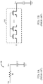
- For example, as illustrated in the RC circuit diagram 100 of
FIG. 1A , a large-valued poly-silicon (poly) resistor R may be used (e.g., having a resistance value on the order of 20 MΩ). However, as discussed above, the poly-resistor R may take up a significant amount of area in an IC. As an alternative, a large resistance value may be attained by cascading transistors 102 (e.g., NMOS or PMOS) operating in the triode region as illustrated inFIG. 1B . With the transistors cascaded in series, the resistance values from each transistor may be summed to obtain a total resistance value. However, in order to obtain a large total resistance value, a large number of transistors may be used. Thus, cascading transistors to realize a large resistive value also takes up a substantial amount of IC real estate. - Accordingly, what is needed are techniques and apparatus for generating a large resistance value with reduced area consumption.
- Certain aspects of the present disclosure provide a robust approach to replacing the large poly resistor, involving employing a tiny metal-oxide semiconductor (MOS) device that is biased in the sub-threshold region. The resistance of the MOS device can be controlled over process, voltage, and temperature (PVT). Using a MOS in sub-threshold as discussed herein may replace the use of poly resistors discussed above, which have large area overhead. Moreover, by using a MOS in sub-threshold, a lower capacitance may also be used in the RC filter because the MOS can have a much larger resistance value than poly resistors can offer, thereby potentially offering even greater area reduction.
-
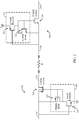
FIG. 2 provides example circuit diagrams of transistor configurations that function as resistors with large electrical resistance valuesFIG. 2 illustrates anexample circuit 202 that is equivalent to a resistor with a large electrical resistance value. The series resistance is generated with a p-channel MOS (PMOS) field-effect transistor (MOSFET) 210 (effectively a "PMOS resistor") operating in the sub-threshold region. For example, the source of thePMOS transistor 210 may be connected to a first node 214 (e.g., an input voltage node), while the drain may be connected to a second node 216 (e.g., an output voltage node). Thus, resistance between a drain and source of thePMOS transistor 210 may be used to attain high resistance between thefirst node 214 and thesecond node 216. - The
PMOS transistor 210 may be biased in the sub-threshold region by abias circuit 206 that is connected with the gate and source of thePMOS transistor 210. Thebias circuit 206 may limit the voltage potential between the gate and source (VGS) of thePMOS transistor 210 with a voltage-limiting device. In certain aspects, the voltage-limiting device may comprise a diode-connected PMOS transistor 224 (referred to as a "PMOS diode"), in which the gate and drain of thePMOS transistor 224 are shorted together. As illustrated in thecircuit 202, the drain and gate of thePMOS transistor 224 may be connected with the gate of thePMOS transistor 210, while the source of thePMOS transistor 224 may be connected with the source of thePMOS transistor 210 and thefirst node 214. In certain aspects, the voltage-limiting device may comprise a diode (not illustrated) having an anode connected with the source of thePMOS transistor 210 and a cathode connected with the gate of thePMOS transistor 210. - Moreover, the
bias circuit 206 may further comprise a current-limiting n-channel MOS (NMOS)transistor 212 having a drain connected with the drain of thePMOS transistor 224 and with the gate of thePMOS transistor 210 and a source connected with a reference potential (e.g., electrical ground). The gate of the current-limitingtransistor 212 may be connected with thefirst node 214. The current-limitingtransistor 212 may be configured to have a small drain-to-source current. In certain aspects, in an effort to reduce leakage current, a bulk and source of thePMOS transistor 210 may be connected together. Similarly, a bulk and source of the diode-connectedPMOS transistor 224 may be connected together. - For other aspects, a large resistance may be generated using an
NMOS transistor 220 operating in the sub-threshold region, as illustrated incircuit 204 ofFIG. 2 . The NMOS transistor 220 (effective an "NMOS resistor") may be connected betweennodes circuit 202, abias circuit 218 may be connected with the source and gate of theNMOS transistor 220 and utilized to bias theNMOS transistor 220 in the sub-threshold region. - The
bias circuit 218 may limit the voltage potential between the gate and source (VGS) of theNMOS transistor 220 with a voltage-limiting device. In certain aspects, the voltage-limiting device may comprise a diode-connected NMOS transistor 226 (referred to as an "NMOS diode"), in which the gate and drain of theNMOS transistor 226 are shorted together. A drain and gate of theNMOS transistor 226 may be connected with the gate of theNMOS transistor 220, while the source of theNMOS transistor 226 may be connected with the source of theNMOS transistor 220 and with thefirst node 214. In certain aspects, the voltage-limiting device may comprise a diode (not illustrated) having an anode connected with the gate of theNMOS transistor 220 and a cathode connected with the source of theNMOS transistor 220. Moreover, thebias circuit 218 may further comprise a current-limitingPMOS transistor 222 having a drain connected with the gate of theNMOS transistor 220 and a source connected with a power supply voltage (e.g., VSS). The gate of the current-limitingPMOS transistor 222 may be connected with thefirst node 214. The current-limitingPMOS transistor 222 may be configured to have a small source-to-drain current. For certain aspects, a bulk and source of theNMOS transistor 222 may be connected together. Similarly, the bulk and source of the diode-connectedNMOS transistor 226 may be connected together, although not shown inFIG. 2 . - Certain aspects of the present disclosure add a
PMOS transistor 304 to thecircuit 202, where thePMOS transistor 304 is configured to function as a fast charge (FC) switch and may be connected in parallel with thePMOS transistor 210, as illustrated inFIG. 3 . For example, a source of thePMOS transistor 304 may be connected with the drain of thePMOS transistor 210, while a drain of thePMOS transistor 304 may be connected with the source of thePMOS resistor 210. The gate of thePMOS transistor 304 may be driven to bias thePMOS transistor 304 in a saturation (active) region in order to effectively short circuit and bypass the drain-to-source resistance of thePMOS transistor 210. Thus, by placing thePMOS transistor 304 in saturation, thecapacitor 302 may be charged at an increased rate (hence the term "fast charge switch"). In certain aspects, a bulk and source of thePMOS transistor 304 may be connected together in an effort to reduce leakage current. - Similarly, other aspects add an
NMOS transistor 404 to thecircuit 204, where theNMOS transistor 404 is configured to function as an FC switch and may be connected in parallel with theNMOS transistor 220, as illustrated inFIG. 4 . In certain aspects, a source and a bulk of theNMOS transistor 404 may be connected together in an effort to reduce leakage current. Moreover, theNMOS transistor 404 may be a deep n-well NMOS transistor to reduce substrate leakage current. -
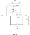
FIG. 5 is acircuit 500 illustrating an example usage of thecircuit 202 as the resistance in a first order low-pass filter of a current mirror, in accordance with certain aspects of the present disclosure. A current mirror is a type of current amplifier that provides a high impedance output current proportional to an input current. The output current (Iout) is typically used to drive a load for high gain. A simple current mirror as shown inFIG. 5 generally consists of a pair oftransistors input transistor 502. InFIG. 5 , the gates of thetransistors transistors - The sources of the
transistors FIG. 5 ) that is common to both transistors. The drain and gate of theinput transistor 502 are connected together and to a current source that provides a quiescent reference current (Ibias). Because the input andoutput transistors output transistor 504. Generally, the input andoutput transistors -
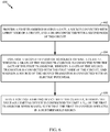
FIG. 6 is a flow diagram ofexample operations 600 for generating a large electrical resistance between first and second nodes of a circuit, in accordance with certain aspects of the present disclosure. Theoperations 600 may be performed, for example, by any of the circuits described above, such as thecircuits - The
operations 600 may begin, atblock 602, by providing a first transistor. The first transistor may have a gate, a source connected with a first node of a circuit, and a drain connected with a second node of the circuit. - At
block 604, a second transistor may be controlled to source or sink a current. A drain of the second transistor may be connected with the gate of the first transistor, a gate of the second transistor may be connected with the first node of the circuit, and a source of the second transistor is connected with an electric potential (e.g., electrical ground or a power supply rail). - At
block 606, a voltage-limiting device may be forward biased with the current. The voltage-limiting device may be connected between the gate and the source of the first transistor. The voltage-limiting device may be configured to limit a VGS of the first transistor when forward biased, such that the first transistor operates in a sub-threshold region. - The various operations or methods described above may be performed by any suitable means capable of performing the corresponding functions. The means may include various hardware and/or software component(s) and/or module(s), including, but not limited to a circuit, an application specific integrated circuit (ASIC), or processor. Generally, where there are operations illustrated in figures, those operations may have corresponding counterpart means-plus-function components with similar numbering.
- For example, means for sourcing or sinking a current may comprise a current-limiting transistor, such as the
NMOS transistor 212 or thePMOS transistor 222 depicted inFIG. 2 . Means for limiting a gate-to-source voltage (VGS) of a transistor may include a voltage-limiting device, such as a diode or a diode-connected transistor (e.g.,PMOS transistor 224 orNMOS transistor 226 inFIG. 2 ). - As used herein, the term "determining" encompasses a wide variety of actions. For example, "determining" may include calculating, computing, processing, deriving, investigating, looking up (e.g., looking up in a table, a database or another data structure), ascertaining and the like. Also, "determining" may include receiving (e.g., receiving information), accessing (e.g., accessing data in a memory) and the like. Also, "determining" may include resolving, selecting, choosing, establishing and the like.
- As used herein, a phrase referring to "at least one of' a list of items refers to any combination of those items, including single members. As an example, "at least one of: a, b, or c" is intended to cover: a, b, c, a-b, a-c, b-c, a-b-c, as well as any combination with multiples of the same element (e.g., a-a, a-a-a, a-a-b, a-a-c, a-b-b, a-c-c, b-b, b-b-b, b-b-c, c-c, and c-c-c or any other ordering of a, b, and c).
- The methods disclosed herein comprise one or more steps or actions for achieving the described method. The method steps and/or actions may be interchanged with one another without departing from the scope of the claims. In other words, unless a specific order of steps or actions is specified, the order and/or use of specific steps and/or actions may be modified without departing from the scope of the claims.
- It is to be understood that the claims are not limited to the precise configuration and components illustrated above. Various modifications, changes and variations may be made in the arrangement, operation and details of the methods and apparatus described above without departing from the scope of the claims.
Claims (15)
- A circuit (202, 204), comprising:a first transistor (210, 220) having a gate, a source connected with a first node (214) of the circuit (202, 204), and a drain connected with a second node (216) of the circuit (202, 204);a voltage-limiting device (224, 226) connected between the gate and the source of the first transistor (210, 220), wherein the device (224, 226), if forward biased, is configured to limit a gate-to-source voltage, VGS, of the first transistor (210, 220) such that the first transistor (210, 220) operates in a sub-threshold region; anda second transistor (212, 222) configured to bias the voltage-limiting device (224, 226) with a current, wherein:a drain of the second transistor (212, 222) is connected with the gate of the first transistor (210, 220);a gate of the second transistor (212, 222) is connected with the first node (214) ; anda source of the second transistor (212, 222) is connected with an electric potential.
- The circuit (202, 204) of claim 1, wherein the voltage-limiting device (224, 226) comprises a diode-connected transistor (224, 226), preferably,
wherein a gate and a drain of the diode-connected transistor (224, 226) are connected with the gate of the first transistor (210, 220) and wherein a source of the diode-connected transistor (224, 226) is connected with the source of the first transistor (210, 220), preferably,
wherein the source and a bulk of the diode-connected transistor (224, 226) are connected together. - The circuit (202, 204) of claim 1, wherein the source and a bulk of the first transistor (210, 220) are connected together.
- The circuit (202, 204) of claim 1, further comprising a third transistor (304) connected in parallel with the first transistor (210, 220), wherein a gate of the third transistor (304) is configured to control bypassing of the first transistor (210, 220), preferably,
wherein a bulk and a source of the third transistor (304) are connected together. - The circuit (202, 204) of claim 1, further comprising a capacitor (302, 402) connected between the second node (216) and an electrical ground, preferably,
wherein the circuit (202, 204) comprises a filter, wherein the first node (214) is an input of the filter, and wherein the second node (216) is an output of the filter. - The circuit (202, 204) of claim 1, wherein the electric potential is an electrical ground.
- The circuit (202, 204) of claim 1, wherein the first transistor (210, 220) is a PMOS transistor.
- The circuit (202, 204) of claim 7, wherein the voltage-limiting device (224, 226) comprises a diode-connected PMOS transistor.
- The circuit (202, 204) of claim 8, wherein the second transistor (212, 222) is an NMOS transistor.
- The circuit (202, 204) of claim 7, wherein the voltage-limiting device (224, 226) comprises a diode having an anode connected with the source of the first transistor (210, 220) and a cathode connected with the gate of the first transistor (210, 220).
- The circuit (202, 204) of claim 1, wherein the first transistor (210, 220) is an NMOS transistor.
- The circuit (202, 204) of claim 11, wherein the voltage-limiting device (224, 226) comprises a diode-connected NMOS transistor.
- The circuit (202, 204) of claim 12, wherein the second transistor (212, 222) is a PMOS transistor.
- The circuit (202, 204) of claim 11, wherein the voltage-limiting device (224, 226) comprises a diode having an anode connected with the gate of the first transistor (210, 220) and a cathode connected with the source of the first transistor (210, 220).
- A method, comprising:providing (602) a first transistor (210, 220) having a gate, a source connected with a first node (214) of a circuit (202, 204), and a drain connected with a second node (216) of the circuit (202, 204);controlling (604) a second transistor (212, 222) to source or sink a current, wherein:forward biasing (606) a voltage-limiting device (224, 226) with the current, wherein the voltage-limiting device (224, 226) is connected between the gate and the source of the first transistor (210, 220) and wherein the voltage-limiting device (224, 226) is configured to limit a gate-to-source voltage, VGS, of the first transistor (210, 220) when forward biased, such that the first transistor (210, 220) operates in a sub-threshold region.a drain of the second transistor (212, 222) is connected with the gate of the first transistor (210, 220);a gate of the second transistor (212, 222) is connected with the first node (214) of the circuit (202, 204); anda source of the second transistor (212, 222) is connected with an electric potential; and
Applications Claiming Priority (3)
| Application Number | Priority Date | Filing Date | Title |
|---|---|---|---|
| US201462089927P | 2014-12-10 | 2014-12-10 | |
| US14/642,309 US10128823B2 (en) | 2014-12-10 | 2015-03-09 | Subthreshold metal oxide semiconductor for large resistance |
| PCT/US2015/059451 WO2016093991A1 (en) | 2014-12-10 | 2015-11-06 | Subthreshold metal oxide semiconductor for large resistance |
Publications (2)
| Publication Number | Publication Date |
|---|---|
| EP3231088A1 EP3231088A1 (en) | 2017-10-18 |
| EP3231088B1 true EP3231088B1 (en) | 2020-07-22 |
Family
ID=54557494
Family Applications (1)
| Application Number | Title | Priority Date | Filing Date |
|---|---|---|---|
| EP15797226.6A Active EP3231088B1 (en) | 2014-12-10 | 2015-11-06 | Subthreshold metal oxide semiconductor for large resistance |
Country Status (6)
| Country | Link |
|---|---|
| US (1) | US10128823B2 (en) |
| EP (1) | EP3231088B1 (en) |
| JP (1) | JP6710687B2 (en) |
| CN (1) | CN107251429B (en) |
| ES (1) | ES2821452T3 (en) |
| WO (1) | WO2016093991A1 (en) |
Families Citing this family (6)
| Publication number | Priority date | Publication date | Assignee | Title |
|---|---|---|---|---|
| KR20180116842A (en) | 2017-04-18 | 2018-10-26 | 에스케이하이닉스 주식회사 | Synapse System of a Neuromorphic Device Including a Ferroelectric Transistor |
| US10574212B2 (en) * | 2017-11-21 | 2020-02-25 | Mediatek Inc. | Method and circuit for low-noise reference signal generation |
| US10944394B2 (en) * | 2018-09-05 | 2021-03-09 | Texas Instruments Incorporated | Methods and apparatus to reduce leakage current |
| CN110416968A (en) * | 2019-08-09 | 2019-11-05 | 无锡启腾电子科技有限公司 | A kind of electrical fuse and its working method |
| CN114924606A (en) * | 2022-06-02 | 2022-08-19 | 泉芯电子技术(深圳)有限公司 | LDO circuit with low power consumption and high power supply rejection ratio |
| CN115459727A (en) * | 2022-09-20 | 2022-12-09 | 思瑞浦微电子科技(苏州)股份有限公司 | Pseudo resistance circuit, RC filter circuit, current mirror circuit and chip |
Family Cites Families (14)
| Publication number | Priority date | Publication date | Assignee | Title |
|---|---|---|---|---|
| US4682047A (en) * | 1985-08-29 | 1987-07-21 | Siemens Aktiengesellschaft | Complementary metal-oxide-semiconductor input circuit |
| EP0739097B1 (en) | 1995-04-21 | 2004-04-07 | Nippon Telegraph And Telephone Corporation | MOSFET circuit and CMOS logic circuit using the same |
| EP0849878A3 (en) * | 1996-12-19 | 2002-06-26 | Texas Instruments Incorporated | Improvements in or relating to integrated circuits |
| US5973524A (en) | 1998-03-25 | 1999-10-26 | Silsym, Inc. | Obtaining accurate on-chip time-constants and conductances |
| JP3919956B2 (en) * | 1998-10-29 | 2007-05-30 | ローム株式会社 | Impedance change circuit |
| US6392465B1 (en) | 2000-12-18 | 2002-05-21 | National Semiconductor Corporation | Sub-threshold CMOS integrator |
| KR100502972B1 (en) * | 2002-12-04 | 2005-07-26 | 주식회사 코아매직 | Clock generater for Refresh execution |
| US6753726B1 (en) | 2003-01-31 | 2004-06-22 | Sun Microsystems, Inc. | Apparatus and method for an offset-correcting sense amplifier |
| EP1612511B1 (en) | 2004-07-01 | 2015-05-20 | Softkinetic Sensors Nv | TOF rangefinding with large dynamic range and enhanced background radiation suppression |
| JP4764086B2 (en) * | 2005-07-27 | 2011-08-31 | パナソニック株式会社 | Semiconductor integrated circuit device |
| US7800435B2 (en) | 2006-12-11 | 2010-09-21 | Fairchild Semiconductor Corporation | Audio filter using a diode connected MOSFET |
| US8054156B2 (en) | 2008-08-26 | 2011-11-08 | Atmel Corporation | Low variation resistor |
| US8898356B2 (en) * | 2013-03-15 | 2014-11-25 | Microchip Technology Incorporated | Combined power and input/output line |
| US9104223B2 (en) * | 2013-05-14 | 2015-08-11 | Intel IP Corporation | Output voltage variation reduction |
-
2015
- 2015-03-09 US US14/642,309 patent/US10128823B2/en active Active
- 2015-11-06 ES ES15797226T patent/ES2821452T3/en active Active
- 2015-11-06 CN CN201580063665.XA patent/CN107251429B/en active Active
- 2015-11-06 JP JP2017530758A patent/JP6710687B2/en active Active
- 2015-11-06 EP EP15797226.6A patent/EP3231088B1/en active Active
- 2015-11-06 WO PCT/US2015/059451 patent/WO2016093991A1/en active Application Filing
Non-Patent Citations (1)
| Title |
|---|
| None * |
Also Published As
| Publication number | Publication date |
|---|---|
| CN107251429B (en) | 2020-11-03 |
| WO2016093991A1 (en) | 2016-06-16 |
| JP2018506197A (en) | 2018-03-01 |
| US20160173072A1 (en) | 2016-06-16 |
| EP3231088A1 (en) | 2017-10-18 |
| ES2821452T3 (en) | 2021-04-26 |
| JP6710687B2 (en) | 2020-06-17 |
| CN107251429A (en) | 2017-10-13 |
| US10128823B2 (en) | 2018-11-13 |
Similar Documents
| Publication | Publication Date | Title |
|---|---|---|
| EP3231088B1 (en) | Subthreshold metal oxide semiconductor for large resistance | |
| US7746047B2 (en) | Low dropout voltage regulator with improved voltage controlled current source | |
| TWI476557B (en) | Low dropout (ldo) voltage regulator and method therefor | |
| US8742819B2 (en) | Current limiting circuitry and method for pass elements and output stages | |
| KR101018950B1 (en) | Constant voltage outputting circuit | |
| US20160308497A1 (en) | Low drop out voltage regulator and method therefor | |
| TW201339785A (en) | Voltage regulator with adaptive miller compensation | |
| US20120001605A1 (en) | Differential amplifier circuit and series regulator | |
| US8310308B1 (en) | Wide bandwidth class C amplifier with common-mode feedback | |
| US7317358B2 (en) | Differential amplifier circuit | |
| US20200081477A1 (en) | Bandgap reference circuit | |
| JPH10189874A (en) | Impedance element | |
| US9785177B1 (en) | Symmetrical positive and negative reference voltage generation | |
| US20050218993A1 (en) | Fast-response current limiting | |
| JP6912350B2 (en) | Voltage regulator | |
| US7042205B2 (en) | Reference voltage generator with supply voltage and temperature immunity | |
| US10095260B2 (en) | Start-up circuit arranged to initialize a circuit portion | |
| CN115459727A (en) | Pseudo resistance circuit, RC filter circuit, current mirror circuit and chip | |
| US20210216094A1 (en) | Voltage supervisor | |
| US9588540B2 (en) | Supply-side voltage regulator | |
| JP6672067B2 (en) | Stabilized power supply circuit | |
| CN109643137A (en) | Low pressure reference current circuit | |
| JP2798022B2 (en) | Reference voltage circuit | |
| KR20180014309A (en) | Current generating circuit capable of compensating temperature variations using an active element | |
| US10211815B2 (en) | Systems and methods for supplying different voltage levels with shared current |
Legal Events
| Date | Code | Title | Description |
|---|---|---|---|
| STAA | Information on the status of an ep patent application or granted ep patent |
Free format text: STATUS: THE INTERNATIONAL PUBLICATION HAS BEEN MADE |
|
| PUAI | Public reference made under article 153(3) epc to a published international application that has entered the european phase |
Free format text: ORIGINAL CODE: 0009012 |
|
| STAA | Information on the status of an ep patent application or granted ep patent |
Free format text: STATUS: REQUEST FOR EXAMINATION WAS MADE |
|
| 17P | Request for examination filed |
Effective date: 20170425 |
|
| AK | Designated contracting states |
Kind code of ref document: A1 Designated state(s): AL AT BE BG CH CY CZ DE DK EE ES FI FR GB GR HR HU IE IS IT LI LT LU LV MC MK MT NL NO PL PT RO RS SE SI SK SM TR |
|
| AX | Request for extension of the european patent |
Extension state: BA ME |
|
| DAV | Request for validation of the european patent (deleted) | ||
| DAX | Request for extension of the european patent (deleted) | ||
| GRAP | Despatch of communication of intention to grant a patent |
Free format text: ORIGINAL CODE: EPIDOSNIGR1 |
|
| STAA | Information on the status of an ep patent application or granted ep patent |
Free format text: STATUS: GRANT OF PATENT IS INTENDED |
|
| INTG | Intention to grant announced |
Effective date: 20200220 |
|
| GRAS | Grant fee paid |
Free format text: ORIGINAL CODE: EPIDOSNIGR3 |
|
| GRAA | (expected) grant |
Free format text: ORIGINAL CODE: 0009210 |
|
| STAA | Information on the status of an ep patent application or granted ep patent |
Free format text: STATUS: THE PATENT HAS BEEN GRANTED |
|
| AK | Designated contracting states |
Kind code of ref document: B1 Designated state(s): AL AT BE BG CH CY CZ DE DK EE ES FI FR GB GR HR HU IE IS IT LI LT LU LV MC MK MT NL NO PL PT RO RS SE SI SK SM TR |
|
| REG | Reference to a national code |
Ref country code: GB Ref legal event code: FG4D |
|
| REG | Reference to a national code |
Ref country code: CH Ref legal event code: EP Ref country code: CH Ref legal event code: NV Representative=s name: MAUCHER JENKINS PATENTANWAELTE AND RECHTSANWAE, DE |
|
| REG | Reference to a national code |
Ref country code: DE Ref legal event code: R096 Ref document number: 602015056231 Country of ref document: DE |
|
| REG | Reference to a national code |
Ref country code: AT Ref legal event code: REF Ref document number: 1294350 Country of ref document: AT Kind code of ref document: T Effective date: 20200815 |
|
| REG | Reference to a national code |
Ref country code: IE Ref legal event code: FG4D |
|
| REG | Reference to a national code |
Ref country code: SE Ref legal event code: TRGR |
|
| REG | Reference to a national code |
Ref country code: DE Ref legal event code: R082 Ref document number: 602015056231 Country of ref document: DE Representative=s name: WAGNER & GEYER PARTNERSCHAFT MBB PATENT- UND R, DE Ref country code: DE Ref legal event code: R081 Ref document number: 602015056231 Country of ref document: DE Owner name: QUALCOMM INCORPORATED, SAN DIEGO, US Free format text: FORMER OWNER: QUALCOMM INC., SAN DIEGO, CALIF., US |
|
| REG | Reference to a national code |
Ref country code: NL Ref legal event code: FP |
|
| REG | Reference to a national code |
Ref country code: NO Ref legal event code: T2 Effective date: 20200722 |
|
| REG | Reference to a national code |
Ref country code: LT Ref legal event code: MG4D |
|
| REG | Reference to a national code |
Ref country code: AT Ref legal event code: MK05 Ref document number: 1294350 Country of ref document: AT Kind code of ref document: T Effective date: 20200722 |
|
| PG25 | Lapsed in a contracting state [announced via postgrant information from national office to epo] |
Ref country code: BG Free format text: LAPSE BECAUSE OF FAILURE TO SUBMIT A TRANSLATION OF THE DESCRIPTION OR TO PAY THE FEE WITHIN THE PRESCRIBED TIME-LIMIT Effective date: 20201022 Ref country code: LT Free format text: LAPSE BECAUSE OF FAILURE TO SUBMIT A TRANSLATION OF THE DESCRIPTION OR TO PAY THE FEE WITHIN THE PRESCRIBED TIME-LIMIT Effective date: 20200722 Ref country code: PT Free format text: LAPSE BECAUSE OF FAILURE TO SUBMIT A TRANSLATION OF THE DESCRIPTION OR TO PAY THE FEE WITHIN THE PRESCRIBED TIME-LIMIT Effective date: 20201123 Ref country code: AT Free format text: LAPSE BECAUSE OF FAILURE TO SUBMIT A TRANSLATION OF THE DESCRIPTION OR TO PAY THE FEE WITHIN THE PRESCRIBED TIME-LIMIT Effective date: 20200722 Ref country code: HR Free format text: LAPSE BECAUSE OF FAILURE TO SUBMIT A TRANSLATION OF THE DESCRIPTION OR TO PAY THE FEE WITHIN THE PRESCRIBED TIME-LIMIT Effective date: 20200722 Ref country code: GR Free format text: LAPSE BECAUSE OF FAILURE TO SUBMIT A TRANSLATION OF THE DESCRIPTION OR TO PAY THE FEE WITHIN THE PRESCRIBED TIME-LIMIT Effective date: 20201023 Ref country code: FI Free format text: LAPSE BECAUSE OF FAILURE TO SUBMIT A TRANSLATION OF THE DESCRIPTION OR TO PAY THE FEE WITHIN THE PRESCRIBED TIME-LIMIT Effective date: 20200722 |
|
| PG25 | Lapsed in a contracting state [announced via postgrant information from national office to epo] |
Ref country code: RS Free format text: LAPSE BECAUSE OF FAILURE TO SUBMIT A TRANSLATION OF THE DESCRIPTION OR TO PAY THE FEE WITHIN THE PRESCRIBED TIME-LIMIT Effective date: 20200722 Ref country code: LV Free format text: LAPSE BECAUSE OF FAILURE TO SUBMIT A TRANSLATION OF THE DESCRIPTION OR TO PAY THE FEE WITHIN THE PRESCRIBED TIME-LIMIT Effective date: 20200722 Ref country code: PL Free format text: LAPSE BECAUSE OF FAILURE TO SUBMIT A TRANSLATION OF THE DESCRIPTION OR TO PAY THE FEE WITHIN THE PRESCRIBED TIME-LIMIT Effective date: 20200722 Ref country code: IS Free format text: LAPSE BECAUSE OF FAILURE TO SUBMIT A TRANSLATION OF THE DESCRIPTION OR TO PAY THE FEE WITHIN THE PRESCRIBED TIME-LIMIT Effective date: 20201122 |
|
| REG | Reference to a national code |
Ref country code: DE Ref legal event code: R097 Ref document number: 602015056231 Country of ref document: DE |
|
| REG | Reference to a national code |
Ref country code: ES Ref legal event code: FG2A Ref document number: 2821452 Country of ref document: ES Kind code of ref document: T3 Effective date: 20210426 |
|
| PG25 | Lapsed in a contracting state [announced via postgrant information from national office to epo] |
Ref country code: CZ Free format text: LAPSE BECAUSE OF FAILURE TO SUBMIT A TRANSLATION OF THE DESCRIPTION OR TO PAY THE FEE WITHIN THE PRESCRIBED TIME-LIMIT Effective date: 20200722 Ref country code: DK Free format text: LAPSE BECAUSE OF FAILURE TO SUBMIT A TRANSLATION OF THE DESCRIPTION OR TO PAY THE FEE WITHIN THE PRESCRIBED TIME-LIMIT Effective date: 20200722 Ref country code: IT Free format text: LAPSE BECAUSE OF FAILURE TO SUBMIT A TRANSLATION OF THE DESCRIPTION OR TO PAY THE FEE WITHIN THE PRESCRIBED TIME-LIMIT Effective date: 20200722 Ref country code: EE Free format text: LAPSE BECAUSE OF FAILURE TO SUBMIT A TRANSLATION OF THE DESCRIPTION OR TO PAY THE FEE WITHIN THE PRESCRIBED TIME-LIMIT Effective date: 20200722 Ref country code: RO Free format text: LAPSE BECAUSE OF FAILURE TO SUBMIT A TRANSLATION OF THE DESCRIPTION OR TO PAY THE FEE WITHIN THE PRESCRIBED TIME-LIMIT Effective date: 20200722 Ref country code: SM Free format text: LAPSE BECAUSE OF FAILURE TO SUBMIT A TRANSLATION OF THE DESCRIPTION OR TO PAY THE FEE WITHIN THE PRESCRIBED TIME-LIMIT Effective date: 20200722 |
|
| PLBE | No opposition filed within time limit |
Free format text: ORIGINAL CODE: 0009261 |
|
| STAA | Information on the status of an ep patent application or granted ep patent |
Free format text: STATUS: NO OPPOSITION FILED WITHIN TIME LIMIT |
|
| PG25 | Lapsed in a contracting state [announced via postgrant information from national office to epo] |
Ref country code: AL Free format text: LAPSE BECAUSE OF FAILURE TO SUBMIT A TRANSLATION OF THE DESCRIPTION OR TO PAY THE FEE WITHIN THE PRESCRIBED TIME-LIMIT Effective date: 20200722 |
|
| 26N | No opposition filed |
Effective date: 20210423 |
|
| PG25 | Lapsed in a contracting state [announced via postgrant information from national office to epo] |
Ref country code: MC Free format text: LAPSE BECAUSE OF FAILURE TO SUBMIT A TRANSLATION OF THE DESCRIPTION OR TO PAY THE FEE WITHIN THE PRESCRIBED TIME-LIMIT Effective date: 20200722 Ref country code: SK Free format text: LAPSE BECAUSE OF FAILURE TO SUBMIT A TRANSLATION OF THE DESCRIPTION OR TO PAY THE FEE WITHIN THE PRESCRIBED TIME-LIMIT Effective date: 20200722 |
|
| PG25 | Lapsed in a contracting state [announced via postgrant information from national office to epo] |
Ref country code: LU Free format text: LAPSE BECAUSE OF NON-PAYMENT OF DUE FEES Effective date: 20201106 |
|
| REG | Reference to a national code |
Ref country code: BE Ref legal event code: MM Effective date: 20201130 |
|
| PG25 | Lapsed in a contracting state [announced via postgrant information from national office to epo] |
Ref country code: SI Free format text: LAPSE BECAUSE OF FAILURE TO SUBMIT A TRANSLATION OF THE DESCRIPTION OR TO PAY THE FEE WITHIN THE PRESCRIBED TIME-LIMIT Effective date: 20200722 |
|
| PG25 | Lapsed in a contracting state [announced via postgrant information from national office to epo] |
Ref country code: IE Free format text: LAPSE BECAUSE OF NON-PAYMENT OF DUE FEES Effective date: 20201106 |
|
| PG25 | Lapsed in a contracting state [announced via postgrant information from national office to epo] |
Ref country code: TR Free format text: LAPSE BECAUSE OF FAILURE TO SUBMIT A TRANSLATION OF THE DESCRIPTION OR TO PAY THE FEE WITHIN THE PRESCRIBED TIME-LIMIT Effective date: 20200722 Ref country code: MT Free format text: LAPSE BECAUSE OF FAILURE TO SUBMIT A TRANSLATION OF THE DESCRIPTION OR TO PAY THE FEE WITHIN THE PRESCRIBED TIME-LIMIT Effective date: 20200722 Ref country code: CY Free format text: LAPSE BECAUSE OF FAILURE TO SUBMIT A TRANSLATION OF THE DESCRIPTION OR TO PAY THE FEE WITHIN THE PRESCRIBED TIME-LIMIT Effective date: 20200722 |
|
| PG25 | Lapsed in a contracting state [announced via postgrant information from national office to epo] |
Ref country code: MK Free format text: LAPSE BECAUSE OF FAILURE TO SUBMIT A TRANSLATION OF THE DESCRIPTION OR TO PAY THE FEE WITHIN THE PRESCRIBED TIME-LIMIT Effective date: 20200722 |
|
| PG25 | Lapsed in a contracting state [announced via postgrant information from national office to epo] |
Ref country code: BE Free format text: LAPSE BECAUSE OF NON-PAYMENT OF DUE FEES Effective date: 20201130 |
|
| PGFP | Annual fee paid to national office [announced via postgrant information from national office to epo] |
Ref country code: NL Payment date: 20231012 Year of fee payment: 9 |
|
| PGFP | Annual fee paid to national office [announced via postgrant information from national office to epo] |
Ref country code: GB Payment date: 20231013 Year of fee payment: 9 |
|
| PGFP | Annual fee paid to national office [announced via postgrant information from national office to epo] |
Ref country code: ES Payment date: 20231208 Year of fee payment: 9 |
|
| PGFP | Annual fee paid to national office [announced via postgrant information from national office to epo] |
Ref country code: SE Payment date: 20231108 Year of fee payment: 9 Ref country code: NO Payment date: 20231026 Year of fee payment: 9 Ref country code: FR Payment date: 20231010 Year of fee payment: 9 Ref country code: DE Payment date: 20231010 Year of fee payment: 9 Ref country code: CH Payment date: 20231202 Year of fee payment: 9 |