EP3229227A1 - Display apparatus - Google Patents
Display apparatus Download PDFInfo
- Publication number
- EP3229227A1 EP3229227A1 EP17163389.4A EP17163389A EP3229227A1 EP 3229227 A1 EP3229227 A1 EP 3229227A1 EP 17163389 A EP17163389 A EP 17163389A EP 3229227 A1 EP3229227 A1 EP 3229227A1
- Authority
- EP
- European Patent Office
- Prior art keywords
- display
- display part
- gate
- pixel
- disposed
- Prior art date
- Legal status (The legal status is an assumption and is not a legal conclusion. Google has not performed a legal analysis and makes no representation as to the accuracy of the status listed.)
- Withdrawn
Links
- 230000000903 blocking effect Effects 0.000 claims abstract description 72
- 238000002834 transmittance Methods 0.000 claims description 31
- 239000003086 colorant Substances 0.000 description 7
- 239000011159 matrix material Substances 0.000 description 6
- 239000003990 capacitor Substances 0.000 description 4
- 239000004973 liquid crystal related substance Substances 0.000 description 4
- DYDCUQKUCUHJBH-UWTATZPHSA-N D-Cycloserine Chemical compound N[C@@H]1CONC1=O DYDCUQKUCUHJBH-UWTATZPHSA-N 0.000 description 3
- 102100040862 Dual specificity protein kinase CLK1 Human genes 0.000 description 3
- 102100040844 Dual specificity protein kinase CLK2 Human genes 0.000 description 3
- 101000749294 Homo sapiens Dual specificity protein kinase CLK1 Proteins 0.000 description 3
- 101000749291 Homo sapiens Dual specificity protein kinase CLK2 Proteins 0.000 description 3
- 238000010586 diagram Methods 0.000 description 2
- 239000000463 material Substances 0.000 description 2
- 238000012986 modification Methods 0.000 description 2
- 230000004048 modification Effects 0.000 description 2
- 239000000758 substrate Substances 0.000 description 2
- 101000685663 Homo sapiens Sodium/nucleoside cotransporter 1 Proteins 0.000 description 1
- 101000821827 Homo sapiens Sodium/nucleoside cotransporter 2 Proteins 0.000 description 1
- 101000822028 Homo sapiens Solute carrier family 28 member 3 Proteins 0.000 description 1
- 102100023116 Sodium/nucleoside cotransporter 1 Human genes 0.000 description 1
- 102100021541 Sodium/nucleoside cotransporter 2 Human genes 0.000 description 1
- 102100021470 Solute carrier family 28 member 3 Human genes 0.000 description 1
- 239000011358 absorbing material Substances 0.000 description 1
- 239000007769 metal material Substances 0.000 description 1
- 230000003252 repetitive effect Effects 0.000 description 1
- 230000001360 synchronised effect Effects 0.000 description 1
- 230000007704 transition Effects 0.000 description 1
- 230000000007 visual effect Effects 0.000 description 1
Images






Classifications
-
- G—PHYSICS
- G09—EDUCATION; CRYPTOGRAPHY; DISPLAY; ADVERTISING; SEALS
- G09G—ARRANGEMENTS OR CIRCUITS FOR CONTROL OF INDICATING DEVICES USING STATIC MEANS TO PRESENT VARIABLE INFORMATION
- G09G3/00—Control arrangements or circuits, of interest only in connection with visual indicators other than cathode-ray tubes
- G09G3/20—Control arrangements or circuits, of interest only in connection with visual indicators other than cathode-ray tubes for presentation of an assembly of a number of characters, e.g. a page, by composing the assembly by combination of individual elements arranged in a matrix no fixed position being assigned to or needed to be assigned to the individual characters or partial characters
-
- G—PHYSICS
- G02—OPTICS
- G02F—OPTICAL DEVICES OR ARRANGEMENTS FOR THE CONTROL OF LIGHT BY MODIFICATION OF THE OPTICAL PROPERTIES OF THE MEDIA OF THE ELEMENTS INVOLVED THEREIN; NON-LINEAR OPTICS; FREQUENCY-CHANGING OF LIGHT; OPTICAL LOGIC ELEMENTS; OPTICAL ANALOGUE/DIGITAL CONVERTERS
- G02F1/00—Devices or arrangements for the control of the intensity, colour, phase, polarisation or direction of light arriving from an independent light source, e.g. switching, gating or modulating; Non-linear optics
- G02F1/01—Devices or arrangements for the control of the intensity, colour, phase, polarisation or direction of light arriving from an independent light source, e.g. switching, gating or modulating; Non-linear optics for the control of the intensity, phase, polarisation or colour
- G02F1/13—Devices or arrangements for the control of the intensity, colour, phase, polarisation or direction of light arriving from an independent light source, e.g. switching, gating or modulating; Non-linear optics for the control of the intensity, phase, polarisation or colour based on liquid crystals, e.g. single liquid crystal display cells
- G02F1/133—Constructional arrangements; Operation of liquid crystal cells; Circuit arrangements
- G02F1/1333—Constructional arrangements; Manufacturing methods
- G02F1/1335—Structural association of cells with optical devices, e.g. polarisers or reflectors
- G02F1/133509—Filters, e.g. light shielding masks
- G02F1/133512—Light shielding layers, e.g. black matrix
-
- G—PHYSICS
- G09—EDUCATION; CRYPTOGRAPHY; DISPLAY; ADVERTISING; SEALS
- G09G—ARRANGEMENTS OR CIRCUITS FOR CONTROL OF INDICATING DEVICES USING STATIC MEANS TO PRESENT VARIABLE INFORMATION
- G09G3/00—Control arrangements or circuits, of interest only in connection with visual indicators other than cathode-ray tubes
- G09G3/20—Control arrangements or circuits, of interest only in connection with visual indicators other than cathode-ray tubes for presentation of an assembly of a number of characters, e.g. a page, by composing the assembly by combination of individual elements arranged in a matrix no fixed position being assigned to or needed to be assigned to the individual characters or partial characters
- G09G3/2092—Details of a display terminals using a flat panel, the details relating to the control arrangement of the display terminal and to the interfaces thereto
-
- G—PHYSICS
- G09—EDUCATION; CRYPTOGRAPHY; DISPLAY; ADVERTISING; SEALS
- G09G—ARRANGEMENTS OR CIRCUITS FOR CONTROL OF INDICATING DEVICES USING STATIC MEANS TO PRESENT VARIABLE INFORMATION
- G09G3/00—Control arrangements or circuits, of interest only in connection with visual indicators other than cathode-ray tubes
- G09G3/20—Control arrangements or circuits, of interest only in connection with visual indicators other than cathode-ray tubes for presentation of an assembly of a number of characters, e.g. a page, by composing the assembly by combination of individual elements arranged in a matrix no fixed position being assigned to or needed to be assigned to the individual characters or partial characters
- G09G3/34—Control arrangements or circuits, of interest only in connection with visual indicators other than cathode-ray tubes for presentation of an assembly of a number of characters, e.g. a page, by composing the assembly by combination of individual elements arranged in a matrix no fixed position being assigned to or needed to be assigned to the individual characters or partial characters by control of light from an independent source
- G09G3/36—Control arrangements or circuits, of interest only in connection with visual indicators other than cathode-ray tubes for presentation of an assembly of a number of characters, e.g. a page, by composing the assembly by combination of individual elements arranged in a matrix no fixed position being assigned to or needed to be assigned to the individual characters or partial characters by control of light from an independent source using liquid crystals
-
- G—PHYSICS
- G02—OPTICS
- G02F—OPTICAL DEVICES OR ARRANGEMENTS FOR THE CONTROL OF LIGHT BY MODIFICATION OF THE OPTICAL PROPERTIES OF THE MEDIA OF THE ELEMENTS INVOLVED THEREIN; NON-LINEAR OPTICS; FREQUENCY-CHANGING OF LIGHT; OPTICAL LOGIC ELEMENTS; OPTICAL ANALOGUE/DIGITAL CONVERTERS
- G02F1/00—Devices or arrangements for the control of the intensity, colour, phase, polarisation or direction of light arriving from an independent light source, e.g. switching, gating or modulating; Non-linear optics
- G02F1/01—Devices or arrangements for the control of the intensity, colour, phase, polarisation or direction of light arriving from an independent light source, e.g. switching, gating or modulating; Non-linear optics for the control of the intensity, phase, polarisation or colour
- G02F1/13—Devices or arrangements for the control of the intensity, colour, phase, polarisation or direction of light arriving from an independent light source, e.g. switching, gating or modulating; Non-linear optics for the control of the intensity, phase, polarisation or colour based on liquid crystals, e.g. single liquid crystal display cells
- G02F1/133—Constructional arrangements; Operation of liquid crystal cells; Circuit arrangements
- G02F1/1333—Constructional arrangements; Manufacturing methods
- G02F1/1345—Conductors connecting electrodes to cell terminals
- G02F1/13454—Drivers integrated on the active matrix substrate
-
- G—PHYSICS
- G02—OPTICS
- G02F—OPTICAL DEVICES OR ARRANGEMENTS FOR THE CONTROL OF LIGHT BY MODIFICATION OF THE OPTICAL PROPERTIES OF THE MEDIA OF THE ELEMENTS INVOLVED THEREIN; NON-LINEAR OPTICS; FREQUENCY-CHANGING OF LIGHT; OPTICAL LOGIC ELEMENTS; OPTICAL ANALOGUE/DIGITAL CONVERTERS
- G02F1/00—Devices or arrangements for the control of the intensity, colour, phase, polarisation or direction of light arriving from an independent light source, e.g. switching, gating or modulating; Non-linear optics
- G02F1/01—Devices or arrangements for the control of the intensity, colour, phase, polarisation or direction of light arriving from an independent light source, e.g. switching, gating or modulating; Non-linear optics for the control of the intensity, phase, polarisation or colour
- G02F1/13—Devices or arrangements for the control of the intensity, colour, phase, polarisation or direction of light arriving from an independent light source, e.g. switching, gating or modulating; Non-linear optics for the control of the intensity, phase, polarisation or colour based on liquid crystals, e.g. single liquid crystal display cells
- G02F1/133—Constructional arrangements; Operation of liquid crystal cells; Circuit arrangements
- G02F1/136—Liquid crystal cells structurally associated with a semi-conducting layer or substrate, e.g. cells forming part of an integrated circuit
- G02F1/1362—Active matrix addressed cells
-
- G—PHYSICS
- G09—EDUCATION; CRYPTOGRAPHY; DISPLAY; ADVERTISING; SEALS
- G09G—ARRANGEMENTS OR CIRCUITS FOR CONTROL OF INDICATING DEVICES USING STATIC MEANS TO PRESENT VARIABLE INFORMATION
- G09G3/00—Control arrangements or circuits, of interest only in connection with visual indicators other than cathode-ray tubes
- G09G3/20—Control arrangements or circuits, of interest only in connection with visual indicators other than cathode-ray tubes for presentation of an assembly of a number of characters, e.g. a page, by composing the assembly by combination of individual elements arranged in a matrix no fixed position being assigned to or needed to be assigned to the individual characters or partial characters
- G09G3/22—Control arrangements or circuits, of interest only in connection with visual indicators other than cathode-ray tubes for presentation of an assembly of a number of characters, e.g. a page, by composing the assembly by combination of individual elements arranged in a matrix no fixed position being assigned to or needed to be assigned to the individual characters or partial characters using controlled light sources
- G09G3/30—Control arrangements or circuits, of interest only in connection with visual indicators other than cathode-ray tubes for presentation of an assembly of a number of characters, e.g. a page, by composing the assembly by combination of individual elements arranged in a matrix no fixed position being assigned to or needed to be assigned to the individual characters or partial characters using controlled light sources using electroluminescent panels
- G09G3/32—Control arrangements or circuits, of interest only in connection with visual indicators other than cathode-ray tubes for presentation of an assembly of a number of characters, e.g. a page, by composing the assembly by combination of individual elements arranged in a matrix no fixed position being assigned to or needed to be assigned to the individual characters or partial characters using controlled light sources using electroluminescent panels semiconductive, e.g. using light-emitting diodes [LED]
- G09G3/3208—Control arrangements or circuits, of interest only in connection with visual indicators other than cathode-ray tubes for presentation of an assembly of a number of characters, e.g. a page, by composing the assembly by combination of individual elements arranged in a matrix no fixed position being assigned to or needed to be assigned to the individual characters or partial characters using controlled light sources using electroluminescent panels semiconductive, e.g. using light-emitting diodes [LED] organic, e.g. using organic light-emitting diodes [OLED]
- G09G3/3266—Details of drivers for scan electrodes
-
- G—PHYSICS
- G09—EDUCATION; CRYPTOGRAPHY; DISPLAY; ADVERTISING; SEALS
- G09G—ARRANGEMENTS OR CIRCUITS FOR CONTROL OF INDICATING DEVICES USING STATIC MEANS TO PRESENT VARIABLE INFORMATION
- G09G3/00—Control arrangements or circuits, of interest only in connection with visual indicators other than cathode-ray tubes
- G09G3/20—Control arrangements or circuits, of interest only in connection with visual indicators other than cathode-ray tubes for presentation of an assembly of a number of characters, e.g. a page, by composing the assembly by combination of individual elements arranged in a matrix no fixed position being assigned to or needed to be assigned to the individual characters or partial characters
- G09G3/34—Control arrangements or circuits, of interest only in connection with visual indicators other than cathode-ray tubes for presentation of an assembly of a number of characters, e.g. a page, by composing the assembly by combination of individual elements arranged in a matrix no fixed position being assigned to or needed to be assigned to the individual characters or partial characters by control of light from an independent source
- G09G3/36—Control arrangements or circuits, of interest only in connection with visual indicators other than cathode-ray tubes for presentation of an assembly of a number of characters, e.g. a page, by composing the assembly by combination of individual elements arranged in a matrix no fixed position being assigned to or needed to be assigned to the individual characters or partial characters by control of light from an independent source using liquid crystals
- G09G3/3611—Control of matrices with row and column drivers
- G09G3/3648—Control of matrices with row and column drivers using an active matrix
- G09G3/3659—Control of matrices with row and column drivers using an active matrix the addressing of the pixel involving the control of two or more scan electrodes or two or more data electrodes, e.g. pixel voltage dependant on signal of two data electrodes
-
- G—PHYSICS
- G09—EDUCATION; CRYPTOGRAPHY; DISPLAY; ADVERTISING; SEALS
- G09G—ARRANGEMENTS OR CIRCUITS FOR CONTROL OF INDICATING DEVICES USING STATIC MEANS TO PRESENT VARIABLE INFORMATION
- G09G3/00—Control arrangements or circuits, of interest only in connection with visual indicators other than cathode-ray tubes
- G09G3/20—Control arrangements or circuits, of interest only in connection with visual indicators other than cathode-ray tubes for presentation of an assembly of a number of characters, e.g. a page, by composing the assembly by combination of individual elements arranged in a matrix no fixed position being assigned to or needed to be assigned to the individual characters or partial characters
- G09G3/34—Control arrangements or circuits, of interest only in connection with visual indicators other than cathode-ray tubes for presentation of an assembly of a number of characters, e.g. a page, by composing the assembly by combination of individual elements arranged in a matrix no fixed position being assigned to or needed to be assigned to the individual characters or partial characters by control of light from an independent source
- G09G3/36—Control arrangements or circuits, of interest only in connection with visual indicators other than cathode-ray tubes for presentation of an assembly of a number of characters, e.g. a page, by composing the assembly by combination of individual elements arranged in a matrix no fixed position being assigned to or needed to be assigned to the individual characters or partial characters by control of light from an independent source using liquid crystals
- G09G3/3611—Control of matrices with row and column drivers
- G09G3/3674—Details of drivers for scan electrodes
- G09G3/3677—Details of drivers for scan electrodes suitable for active matrices only
-
- G—PHYSICS
- G09—EDUCATION; CRYPTOGRAPHY; DISPLAY; ADVERTISING; SEALS
- G09G—ARRANGEMENTS OR CIRCUITS FOR CONTROL OF INDICATING DEVICES USING STATIC MEANS TO PRESENT VARIABLE INFORMATION
- G09G2300/00—Aspects of the constitution of display devices
- G09G2300/04—Structural and physical details of display devices
- G09G2300/0404—Matrix technologies
- G09G2300/0408—Integration of the drivers onto the display substrate
-
- G—PHYSICS
- G09—EDUCATION; CRYPTOGRAPHY; DISPLAY; ADVERTISING; SEALS
- G09G—ARRANGEMENTS OR CIRCUITS FOR CONTROL OF INDICATING DEVICES USING STATIC MEANS TO PRESENT VARIABLE INFORMATION
- G09G2310/00—Command of the display device
- G09G2310/02—Addressing, scanning or driving the display screen or processing steps related thereto
- G09G2310/0262—The addressing of the pixel, in a display other than an active matrix LCD, involving the control of two or more scan electrodes or two or more data electrodes, e.g. pixel voltage dependent on signals of two data electrodes
-
- G—PHYSICS
- G09—EDUCATION; CRYPTOGRAPHY; DISPLAY; ADVERTISING; SEALS
- G09G—ARRANGEMENTS OR CIRCUITS FOR CONTROL OF INDICATING DEVICES USING STATIC MEANS TO PRESENT VARIABLE INFORMATION
- G09G2310/00—Command of the display device
- G09G2310/02—Addressing, scanning or driving the display screen or processing steps related thereto
- G09G2310/0264—Details of driving circuits
- G09G2310/0278—Details of driving circuits arranged to drive both scan and data electrodes
-
- G—PHYSICS
- G09—EDUCATION; CRYPTOGRAPHY; DISPLAY; ADVERTISING; SEALS
- G09G—ARRANGEMENTS OR CIRCUITS FOR CONTROL OF INDICATING DEVICES USING STATIC MEANS TO PRESENT VARIABLE INFORMATION
- G09G2310/00—Command of the display device
- G09G2310/08—Details of timing specific for flat panels, other than clock recovery
-
- G—PHYSICS
- G09—EDUCATION; CRYPTOGRAPHY; DISPLAY; ADVERTISING; SEALS
- G09G—ARRANGEMENTS OR CIRCUITS FOR CONTROL OF INDICATING DEVICES USING STATIC MEANS TO PRESENT VARIABLE INFORMATION
- G09G2320/00—Control of display operating conditions
- G09G2320/02—Improving the quality of display appearance
- G09G2320/0233—Improving the luminance or brightness uniformity across the screen
-
- G—PHYSICS
- G09—EDUCATION; CRYPTOGRAPHY; DISPLAY; ADVERTISING; SEALS
- G09G—ARRANGEMENTS OR CIRCUITS FOR CONTROL OF INDICATING DEVICES USING STATIC MEANS TO PRESENT VARIABLE INFORMATION
- G09G3/00—Control arrangements or circuits, of interest only in connection with visual indicators other than cathode-ray tubes
- G09G3/20—Control arrangements or circuits, of interest only in connection with visual indicators other than cathode-ray tubes for presentation of an assembly of a number of characters, e.g. a page, by composing the assembly by combination of individual elements arranged in a matrix no fixed position being assigned to or needed to be assigned to the individual characters or partial characters
- G09G3/34—Control arrangements or circuits, of interest only in connection with visual indicators other than cathode-ray tubes for presentation of an assembly of a number of characters, e.g. a page, by composing the assembly by combination of individual elements arranged in a matrix no fixed position being assigned to or needed to be assigned to the individual characters or partial characters by control of light from an independent source
- G09G3/3406—Control of illumination source
Definitions
- the present invention relates to a display apparatus having a narrow bezel.
- a flat display panel is typically classified into a light-emitting type and a light-receiving type.
- the light-emitting type of flat display panel includes, for example, a plasma display panel and an organic light emitting display panel.
- the flat panel display panel includes a plurality of pixels and a gate driver driving the pixels.
- the gate driver is disposed in a non-display region adjacent to a display region in which the pixels are arranged.
- the display panel has a bezel width corresponding to the non-display region.
- the present invention sets out to provide a display apparatus having a narrow bezel width.
- Embodiments of the inventive concept provide a display apparatus including a display panel including a gate line extending in one direction, a non-display part, a first display part, a third display part, and a second display part disposed between the first and third display parts and a gate driver including a first gate circuit disposed in the non-display part and a second gate circuit disposed in the first display part and applying a gate signal to the gate line.
- the first display part includes a first pixel including a first pixel electrode, a first pixel circuit driving the first pixel electrode, and a first light blocking part overlapped with the first pixel circuit and the second gate circuit
- the second display part includes a second pixel including a second pixel electrode, a second pixel circuit driving the second pixel electrode, and a second light blocking part overlapped with the second pixel circuit
- the third display part includes a third pixel including a third pixel electrode, a third pixel circuit driving the third pixel electrode, and a third light blocking part overlapped with the third pixel circuit
- an area of the second light blocking part is smaller than an area of the first light blocking part and greater than an area of the third light blocking part.
- the gate line may be provided in a plural number, and the second gate circuit may be disposed between adjacent gate lines to each other among the gate lines.
- the second gate circuit may include a first transistor including an input terminal connected to a clock line and an output terminal connected to the gate line.
- the second gate circuit may further include a second transistor including an input terminal connected to a low voltage line and an output terminal connected to the output terminal of the first transistor.
- the second pixel electrode may have an area greater than an area of the first pixel electrode and smaller than an area of the third pixel electrode.
- the gate driver may further include a third gate circuit disposed in the second display part, and the second light blocking part may be overlapped with the third gate circuit.
- An area in which the third gate circuit is disposed is smaller than an area in which the second gate circuit is disposed.
- the number of transistors included in the third gate circuit may be smaller than the number of transistors included in the second gate circuit.
- the display panel may further include a clock line receiving a clock signal and a low voltage line receiving a low voltage
- the gate driver may further include a plurality of second transistors, each of the second transistors may include an input terminal connected to the low voltage line and an output terminal connected to the gate line
- the second gate circuit may include a first transistor including an input terminal connected to the clock line and an output terminal connected to the gate line
- the third gate circuit may include at least one second transistor among the second transistors.
- At least a portion of the low voltage line and at least a portion of the clock line may be disposed in the first and second display parts.
- the second gate circuit may include at least another second transistor among the second transistors.
- the display panel may further include a plurality of data lines extending in another direction different from the one direction, the second gate circuit may be provided in a plural number, an i-th second gate circuit in the one direction among the second gate circuits may be disposed between an i-th data line and an (i+1)-th data line among the data lines, and the number "i" may be an integer equal to or greater than 1.
- the third gate circuit may be provided in a plural number, a third gate circuit in the one direction among the third gate circuits may be disposed between a j-th data line and a (j+1)-th data line among the data lines, and the number "j" may be an integer greater than the number "i".
- the gate line may be provided in a plural number, a k-th second gate circuit in the another direction different from the one direction among the second gate circuits may be disposed between a k-th gate line and a (k+1)-th gate line among the gate lines, and the number "k" may be an integer greater than 1.
- Each of the first display part and the second display part may be provided in a plural number, and the first display parts, the second display parts, and the third display part may be arranged in order of the first display part, the second display part, the third display part, the second display part, and the first display part along the one direction.
- Each of the first, second, and third display parts may be provided in a plural number, and the first, second, and third display parts may be arranged in order of the first display part, the second display part, the third display part, the second display part, the first display part, the second display part, the third display part, the second display part, and the first display part along the one direction.
- the display apparatus may further include a backlight unit configured to include a first part providing a first light to the first display part, a second part providing a second light to the second display part, and a third part providing a third light to the third display part.
- the second light may have an intensity smaller than an intensity of the first light and greater than an intensity of the third light.
- First, second, and third image signals may be respectively applied to the first, second, and third display parts, and the second image signal may have a brightness value smaller than a brightness value of the first image signal and greater than a brightness value of the third image signal with respect to a same grayscale value.
- Embodiments of the inventive concept may provide a display apparatus including a display panel including a gate line extending in one direction, a non-display part, a first display part, a third display part, and a second display part disposed between the first and third display parts and a gate driver including a first gate circuit disposed in the non-display part and a second gate circuit disposed in the first display part.
- the gate driver may be not disposed in the third display part and apply a gate signal to the gate line, and the second display part may have a transmittance greater than a transmittance of the first display part and smaller than a transmittance of the third display part.
- Embodiments of the inventive further concept provide a display apparatus including a display panel including a gate line extending in one direction, a first display part, a third display part, and a second display part disposed between the first and third display parts and a gate driver including a first gate circuit disposed in the first display part and a second gate circuit disposed in the second display part.
- the gate driver is not disposed in the third display part and applies a gate signal to the gate line.
- N1 denotes a number of transistors of the first gate circuit
- the number N2 denotes a number of transistors of the second gate circuit
- the number R1 denotes an area in which the first gate circuit is disposed
- the number R2 denotes an area in which the second gate circuit 250 is disposed.
- Embodiments of the inventive further concept provide a display apparatus including a display panel including a gate line extending in one direction, a non-display part, a first display part, a third display part, a second display part disposed between the first and third display parts, and a gate driver comprising a first gate circuit disposed in the non-display part and a second gate circuit disposed in the first display part.
- the gate driver is not disposed in the third display part and applies a gate signal to the gate line.
- the first display part comprises a first pixel of a first type
- the second display part comprises a second pixel of a second type
- the third display part comprises a third pixel of a third type
- an aperture ratio of the second pixel is greater than an aperture ratio of the first pixel and smaller than an aperture ratio of the third pixel.
- Each pixel may have a light blocking part and a display area that is not overlapped with the light blocking part, and the aperture ratio of each pixel may be a ratio of the display area and the area of the light block part.
- Each pixel column may contain pixels of the same pixel type.
- One or more contiguous columns of pixels of the first type may form the first display part
- one or more contiguous columns of pixels of the second type may form the second display part
- one or more contiguous columns of pixels of the third type may form the third display part.
- the display panel may be apportioned into a plurality of display parts along a pixel row direction, and the plurality of display parts may be arranged in order of the first display part, the second display part, the third display part, the second display part, and the first display part along the pixel row direction.
- the display panel may be apportioned into a plurality of display parts along a pixel row direction, and the plurality of display parts may be arranged in order of the first display part, the second display part, the third display part, the second display part, the first display part, the second display part, the third display part, the second display part, and the first display part along the pixel row direction.
- the second gate circuit of the gate driver is disposed in the first display part, and thus the bezel width of the display apparatus may be reduced.
- the area of the second light blocking part is smaller than the area of the first light blocking part and greater than the area of the third light blocking part. Accordingly, the boundary between the first and third display parts may be prevented from being recognized, which is caused by the difference in transmittance between the first and third display parts when the second gate circuit is disposed in the first display part. As a result, the display quality of the display apparatus may be improved.
- FIG. 1 is a plan view showing a display apparatus 1000 according to an exemplary embodiment of the present invention.
- the display apparatus 1000 includes a display panel DP displaying an image and a panel driver driving the display panel DP.
- the panel driver includes a gate driver GD, a data driver DD, and a controller CTR controlling the gate driver GD and the data driver DD.
- the controller CTR receives a plurality of control signals CS and input image data RGB containing information on the image.
- the controller CTR converts the input image data RGB to output image data RGB' appropriate to an interface between the data driver DD and the display panel DP and applies the output image data RGB' to the data driver DD.
- the controller CTR generates a data control signal D-CS (e.g., an output start signal, a horizontal start signal, etc.) and a gate control signal G-CS on the basis of the control signals CS.
- the data control signal D-CS is applied to the data driver DD
- the gate control signal G-CS is applied to the gate driver GD.
- the gate driver GD sequentially outputs gate signals in response to the gate control signal G-CS provided from the controller CTR.
- the data driver DD converts the output image data RGB' to data voltages in response to the data control signal D-CS provided from the controller CTR and outputs the data voltages.
- the data voltages are applied to the display panel DP.
- the display panel DP includes a plurality of gate lines GL1 to GLn, a plurality of data lines DL1 to DLm (where n and m are natural numbers), signal lines SL, and a plurality of pixels.
- the display panel DP may be, but not limited to, a flat display panel, such as an organic light emitting display panel including an organic light emitting layer or a liquid crystal display panel including a liquid crystal layer.
- the gate lines GL1 to GLn extend in a first direction DR1 and are arranged in a second direction DR2 to be substantially parallel to each other.
- the data lines DL1 to DLm are insulated from the gate lines GL1 to GLn that cross the data lines DL1 to DLm.
- the data lines DL1 to DLm extend in the second direction DR2 and are arranged in the first direction DR1 to be substantially parallel to each other.
- the first direction DR1 may be substantially perpendicular to the second direction DR2.
- the first and second directions DR1 and DR2 may be respectively referred to as one direction and the other direction.
- Each of the pixels displays one of three primary colors of red, green, and blue colors.
- the colors displayed by the pixels are not limited thereto or thereby, and the pixels may further display various colors, e.g., yellow, cyan, and magenta colors, in addition to the red, green, and blue colors.
- the pixels are arranged in a matrix form along the first and second directions DR1 and DR2.
- Each of the pixels is connected to a corresponding data line of the data lines DL1 to DLm and a corresponding gate line of the gate lines GL1 to GLn.
- the display panel DP includes a non-display part NDA and a display part.
- the display part displays the image, and the non-display part NDA does not display the image.
- the pixels are disposed in the display part.
- the pixels are not disposed in the non-display part NDA, and a circuit used to drive the pixels is disposed in the non-display part NDA.
- the display part includes first, second, and third display parts DA1, DA2, and DA3.
- the second display part DA2 is disposed between the first and third display parts DA1 and DA3.
- the non-display part NDA is disposed at a left end of the display panel DP.
- the parts may be arranged in order of "the non-display part NDA/the first display part DA1/the second display part DA2/the third display part DA3" in the first direction DR1.
- the pixels include first, second, and third pixels PX1, PX2, and PX3.
- the first to third display parts DA1 to DA3 include the first to third pixels PX1 to PX3, respectively.
- the gate driver GD may be implemented by "in-pixel gate driver". Accordingly, at least a portion of the gate driver GD may be disposed in the part in which the pixels are disposed.
- the gate driver GD includes a first gate circuit 100 disposed in the non-display part NDA and a second gate circuit 200 disposed in the first display part DA1. Each of the first and second gate circuits 100 and 200 may be provided in a plural number.
- the first gate circuits 100 are arranged in the second direction DR2 to respectively correspond to the gate lines GL1 to GLn.
- the second gate circuits 200 are arranged in a matrix form to correspond to the first pixels PX1.
- an i-th second gate circuit in the first direction DR1 among the second gate circuits 200 is disposed between an i-th data line and an (i+1)-th data line among the data lines DL1 to DLm
- a k-th second gate circuit in the second direction DR2 among the second gate circuits 200 is disposed between a k-th gate line and a (k+1)-th gate line among the gate lines GL1 to GLn.
- Each of "i” and "k” is an integer number equal to or greater than 1, with i ⁇ m and k ⁇ n.
- the display panel DP includes first to n-th stages SG1 to SGn connected to each other in series.
- An k-th stage may be configured to include the first and second gate circuits 100 and 200 disposed in an k-th row.
- the first and second gate circuits 100 and 200 disposed in the k-th row are connected to each other by the signal line SL.
- the first to n-th stages SG1 to SGn are respectively connected to the gate lines GL1 to GLn to respectively apply first to n-th gate signals to the gate lines GL1 to GLn.
- each of the first to n-th stages SG1 to SGn includes two second gate circuits 200, but it is not limited thereto or thereby. That is, each of the first to n-th stages SG1 to SGn may include q or more second gate circuits 200.
- the number "q" is an integer equal to or greater than 3.
- the number "q" is determined depending on a characteristic of each of the gate lines GL1 to GLn.
- the characteristic of each of the gate lines GL1 to GLn may be, but not limited to, an impedance characteristic. For instance, as the impedance of the gate lines GL1 to GLn increases, the number "q" increases.
- the gate driver GD is implemented by the in-pixel gate driver, the second gate circuits 200 are distributed and arranged in the first display part DA1, and thus, an area in which the second gate circuits 200 are disposed is not required. Thus, a width of the non-display part NDA, i.e., a bezel width, may be reduced.
- FIG. 2A is a view showing the first pixel PX1 shown in FIG. 1
- FIG. 2B is a view showing the second pixel PX2 shown in FIG. 1
- FIG. 2C is a view showing the third pixel PX3 shown in FIG. 1 .
- the first pixel PX1 includes a first pixel electrode 310, a first pixel circuit 320, and a first light blocking part 330.
- the first pixel electrode 310 may be, for example, a transmissive electrode or a reflective electrode.
- the first pixel circuit 320 is connected to the first gate line GL1 and the first data line DL1 to drive the first pixel electrode 310.
- the first pixel circuit 320 includes a first switching transistor ST1.
- the first switching transistor ST1 includes an input terminal connected to the first data line DL1, a control terminal connected to the first gate line GL1, and an output terminal connected to the first pixel electrode 310.
- the first pixel circuit 320 may include two or more transistors, may be further connected to other lines in addition to the data line and the gate line, and may be implemented in various ways.
- the first light blocking part 330 is disposed to overlap with the second gate circuit 200 when viewed in a plan view such that at least the second gate circuit 200 is not visible.
- the second gate circuit 200 is disposed spaced apart from the first pixel electrode 310 in the second direction DR2.
- the second gate circuit 200 includes the signal line SL, a first transistor T1, and a second transistor T2.
- the signal line SL includes an on-switching line 213, an off-switching line 216, a low voltage line 215, and a clock line 211.
- at least a portion of each of the on-switching line 213, the off-switching line 216, the low voltage line 215, and the clock line 211 is overlapped with the first light blocking part 330 when viewed in a plan view.
- the first transistor T1 applies the first gate signal of high voltage to the first gate line GL1.
- An input terminal of the first transistor T1 is connected to the clock line 211 to receive a first clock signal from the clock line 211.
- a control terminal of the first transistor T1 is connected to the on-switching line 213 to receive a Q-node signal from the on-switching line 213.
- An output terminal of the first transistor T1 is connected to the first gate line GL1.
- the second transistor T2 applies the first gate line of low voltage to the first gate line GL1.
- An input terminal of the second transistor T2 is connected to the low voltage line 215 to receive the low voltage from the low voltage line 215.
- a control terminal of the second transistor T2 is connected to the off-switching line 216.
- the control terminal of the second transistor T2 receives a second gate signal of the second gate line GL2 (shown in FIG. 1 ) from the off-switching line 216.
- An output terminal of the second transistor T2 is connected to the output terminal of the first transistor T1.
- the first transistor T1 outputs the high voltage of the first clock signal to the first gate line GL1 as the high voltage of the gate voltage in response to the Q-node signal
- the second transistor T2 outputs the low voltage to the first gate line GL1 as the low voltage of the gate voltage in response to the second gate signal of the second gate line GL2 after a predetermined time lapses.
- the first switching transistor ST1 is turned on in response to the high voltage and applies the data voltage from the first data line DL1 to the first pixel electrode 310.
- the first switching transistor ST1 may be turned off in response to the low voltage.
- the second pixel PX2 includes a second pixel electrode 410, a second pixel circuit 420, and a second light blocking part 430.
- the second pixel electrode 410 may be, for example, a transmissive electrode or a reflective electrode.
- the second pixel circuit 420 is connected to the first gate line GL1 and the second data line DL2 to drive the second pixel electrode 410.
- the second pixel circuit 420 includes a second switching transistor ST2.
- the second switching transistor ST2 includes an input terminal connected to the second data line DL2, a control terminal connected to the first gate line GL1, and an output terminal connected to the second pixel electrode 410.
- the second switching transistor ST2 receives the first gate signal from the first gate line GL1.
- the second switching transistor ST2 is turned on in response to the high voltage of the first gate signal and applies the data voltage provided from the second data line DL2 to the second pixel electrode 410.
- the second switching transistor ST2 may be turned off in response to the low voltage of the first gate signal.
- the second light blocking part 430 is disposed to overlap with the second switching transistor ST2 when viewed in a plan view such that at least the second switching transistor ST2 is not visible.
- the third pixel PX3 includes a third pixel electrode 510, a third pixel circuit 520, and a third light blocking part 530.
- the third pixel electrode 510 may be, for example, a transmissive electrode or a reflective electrode.
- the third pixel circuit 520 is connected to the first gate line GL1 and the third data line DL3 to drive the third pixel electrode 510.
- the third pixel circuit 520 includes a third switching transistor ST3.
- the third switching transistor ST3 includes an input terminal connected to the third data line DL3, a control terminal connected to the first gate line GL1, and an output terminal connected to the third pixel electrode 510.
- the third switching transistor ST3 receives the first gate signal from the first gate line GL1.
- the third switching transistor ST3 is turned on in response to the high voltage of the first gate signal and applies the data voltage provided from the third data line DL3 to the third pixel electrode 510.
- the third switching transistor ST3 may be turned off in response to the low voltage of the first gate signal.
- the third light blocking part 530 is disposed to overlap with the third switching transistor ST3 when viewed in a plan view such that at least the third switching transistor ST3 is not visible.
- FIG. 3A is a layout of the pixel shown in FIG. 2A
- FIG. 3B is a layout of the pixel shown in FIG. 2B
- FIG. 3C is a layout of the pixel shown in FIG. 2C
- FIG. 4 is a cross-sectional view taken along a line I-I' of FIG. 3A .
- the first pixel PX1 includes the first pixel electrode 310, the first pixel circuit 320, and the first light blocking part 330.
- the first switching transistor ST1 includes a first gate electrode GE1, a first active pattern AP1, a first source electrode SE1, and a first drain electrode DE1.
- the gate electrode, the source electrode, and the drain electrode of the transistor may be respectively referred to as the control terminal, the input terminal, and the output terminal.
- the first gate electrode GE1 is branched from the first gate line GL1, and the first active pattern AP1 is disposed above the first gate electrode GE1 such that a first insulating layer IL1 is disposed between the first active pattern AP1 and the first gate electrode GE1.
- the first source electrode SE1 is branched to make contact with the first active pattern AP1, and the first drain electrode DE1 is spaced apart from the first source electrode SE1 to make contact with the first active pattern AP1.
- a second insulating layer IL2 covers the first switching transistor ST1.
- the first pixel electrode 310 is disposed on the second insulating layer IL2, and the first pixel electrode 310 makes contact with the first drain electrode DE1 through a first contact hole CNT1 defined through the second insulating layer IL2.
- the lines 211, 213, 215, and 216 extend in the first direction DR1 and are arranged in the second direction DR2 to be spaced apart from each other by a predetermined distance.
- the first transistor T1 includes a second gate electrode GE2, a second active pattern AP2, a second source electrode SE2, and a second drain electrode DE2.
- the second gate electrode GE2 is branched from the on-switching line 213, and the second active pattern AP2 is disposed above the second gate electrode GE2 such that the first insulating layer IL1 is disposed between the second active pattern AP2 and the second gate electrode GE2.
- the one end of the second source electrode SE2 makes contact with the second active pattern AP2, and the other end of the second source electrode SE2 makes contact with the clock line 211 through a second contact hole CNT2 defined through the first insulating layer IL1.
- the one end of the second source electrode SE2 may include two first branch portions extending in a third direction DR3 opposite to the second direction DR2.
- the second drain electrode DE2 includes two first recesses.
- the first recesses are recessed toward the third direction DR3.
- the two branch portions are respectively inserted into the two first recesses. Accordingly, the two first branch portions are overlapped with the two recesses in the first direction DR1.
- the number of the first branch portions and the number of the first recesses may be determined depending on the driving characteristic of the first transistor T1. For instance, three or more first branch portions and first recesses may be applied to the pixel to improve the driving characteristic, i.e., a driving capacity, or to increase a W/L ratio of a channel width of the first transistor T1 to a channel length of the first transistor T1.
- the second transistor T2 includes a third gate electrode GE3, a third active pattern AP3, a third source electrode SE3, and a third drain electrode DE3.
- the third gate electrode GE3 is branched from the off-switching line 216, and the third active pattern AP3 is disposed above the third gate electrode GE3 such that the first insulating layer IL1 is disposed between the third active pattern AP3 and the third gate electrode GE3.
- the third source electrode SE3 makes contact with the third active pattern AP3, and the other end of the third source electrode SE3 makes contact with the low voltage line 215 through a fourth contact hole CNT4 defined through the first insulating layer IL1.
- the one end of the third source electrode SE3 may include two second branch portions extending in the third direction DR3.
- the third drain electrode DE3 includes two second recesses.
- the second branch portions and the second recesses have the similar structure and function as those of the first branch portions and the first recesses, and thus details thereof are omitted.
- the first light blocking part 330 prevents the first switching transistor ST1, the second gate circuit 200, and the first gate line GL1 from being visible.
- the first light blocking part 330 is overlapped with the first switching transistor ST1, the second gate circuit 200, and the first gate line GL1 when viewed in a plan view.
- the first light blocking part 330 has a substantially quadrangular shape and has the same width as the first pixel electrode 310 in the first direction DR1.
- the first light blocking part 330 has a first width W1 in the second direction DR2.
- a transmittance of the display panel DP at an arbitrarily selected area or portion may be defined by a ratio of an area covered by a light blocking part, e.g., the first light blocking part 330, to an area not covered by first light blocking part 330.
- the first light blocking part 330 is interposed between an upper base substrate US of the display panel DP and a common electrode CE and includes a black matrix containing a light absorbing material.
- the first light blocking part 330 is not limited thereto or thereby, and the first light blocking part 330 may have various shapes. That is, the first light blocking part may include a black matrix disposed between a lower base substrate LS of the display panel DP and a liquid crystal LL.
- the first light blocking part 330 may include a metal material having high reflectance or may have a color filter stack structure in which color filters transmitting different colors are stacked. The color filter may be stacked in a structure in which two color filters among a red color filter, a green color filter, and a blue color filter are stacked.
- the second pixel PX2 includes the second pixel electrode 410, the second pixel circuit 420, and the second light blocking part 430.
- the second pixel circuit 420 and the second pixel electrode 410 are respectively similar to the first pixel circuit 320 and the first pixel electrode 310, and thus details thereof are omitted.
- the second light blocking part 430 prevents the second pixel circuit 420 and the first gate line GL1 from being visible.
- the second light blocking part 430 is overlapped with the second pixel circuit 420 and the first gate line GL1 when viewed in a plan view.
- the second light blocking part 430 has a substantially quadrangular shape and has the same width in the first direction DR1 as the second pixel electrode 410.
- the second light blocking part 430 has a second width W2 in the second direction DR2.
- the second light blocking part 430 may include the same material as that of the first light blocking part 330.
- the third pixel PX3 includes the third pixel electrode 510, the third pixel circuit 520, and the third light blocking part 530.
- the third pixel circuit 520 and the third pixel electrode 510 are respectively similar to the first pixel circuit 320 and the first pixel electrode 310, and thus details thereof are omitted.
- the third light blocking part 530 prevents the third pixel circuit 520 and the first gate line GL1 from being visible.
- the third light blocking part 530 is overlapped with the third pixel circuit 520 and the first gate line GL1 when viewed in a plan view.
- the third light blocking part 530 has a substantially quadrangular shape and has the same width in the first direction DR1 as the third pixel electrode 510.
- the third light blocking part 530 has a third width W3 in the second direction DR2.
- the third light blocking part 530 may include the same material as that of the first light blocking part 330.
- the first, second, and third light blocking parts 330, 430, and 530 have different areas from each other.
- the first, second, and third widths W1, W2, and W3 satisfy the following condition of W1>W2>W3.
- the areas of the first, second, and third light blocking parts 330, 430, and 530, respectively referred to as A1, A2, and A3, satisfy the following condition of A1>A2>A3.
- the areas of the first, second, and third pixel electrodes 310, 410, and 510, respectively referred to as S1, S2, and S3, satisfy the following condition of S1 ⁇ S2 ⁇ S3.
- a first transmittance of the first display part DA1 in which the first pixel PX1 is disposed is lowest, a third transmittance of the third display part DA3 in which the third pixel PX3 is disposed is highest, and a second transmittance of the second display part DA2 in which the second pixel PX2 is disposed has a value between the first and third transmittances.
- the second gate circuit 200 since the second gate circuit 200 is disposed in the first display part DA1, a large difference exists between the first and third transmittances.
- the second display part DA2 having the second transmittance is interposed between the first and third display parts DA1 and DA3, a boundary between the first and third display parts DA1 and DA3 may be prevented from being recognized even though the difference in transmittance exists between the first and third display parts DA1 and DA3. That is, the second display part makes the visual transition between the first and third transmittances less abrupt and less recognizable by a viewer of the display apparatus. As a result, a display quality of the display apparatus 1000 (refer to FIG. 1 ) may be improved.
- FIG. 5 is a circuit diagram showing a first stage shown in FIG. 1 .
- a control line CL and the first gate circuit 100 of the first stage SG1 are disposed in the non-display part NDA, and the second gate circuit 200 is disposed in the first display part DA1.
- the control line CL includes a first voltage line VSL1, a first clock line CLK1, a second clock line CLK2, and a vertical start line STL, which are provided to the first stage SG1.
- the control line CL may further include a third clock line and a fourth clock line.
- the first voltage line VSL1 transmits the low voltage
- the first clock line CLK1 transmits the first clock signal
- the second clock line CLK2 transmits the second clock signal
- the vertical start line STL transmits the vertical start signal.
- the first gate circuit 100 includes a buffer part 110, a charge part 120, a carry part 140, a first discharge part 151, a second discharge part 153, a switch part 170, a first maintain part 181, a second maintain part 182, a third maintain part 183, and a fourth maintain part 184.
- the buffer part 110 includes a fourth transistor T4. A control terminal and an input terminal of the buffer part 110 are connected to the vertical start line STL to receive the vertical start signal, and an output terminal of the buffer part 110 is connected to the Q-node Q (or control node). Responsive to the high voltage of the vertical start signal, the buffer part 110 allows the charge part 120 connected to the Q-node Q to be charged with the high voltage of the vertical start signal.
- the charge part 120 includes a boost capacitor Cgs.
- the boost capacitor Cgs includes a first terminal connected to the Q-node Q and a second terminal connected to the first gate line GL1.
- the control terminal of the first transistor T1 is electrically connected to the first terminal of the charge part 120 connected to the Q-node Q through the on-switching line 213, the input terminal of the first transistor T1 receives the first clock signal through the clock line 211 connected to the first clock line CLK1, and the output terminal is connected to the first gate line GL1.
- the boost capacitor Cgs boosts the voltage charged therein.
- the first transistor T1 applies the high voltage of the first clock signal to the first gate line GL1 in response to the boosted voltage.
- the carry part 140 includes a fifteenth transistor T15.
- a control terminal of the carry part 140 is connected to the Q-node Q, an input terminal of the carry part 140 receives the first clock signal, and an output terminal of the carry part 140 is connected to one stage among the next stages following the carry part 140.
- the carry part 140 applies the high voltage of the first clock signal to the second stage SG2 as a first carry signal CR1.
- the discharge part 151 includes a ninth transistor T9.
- a control terminal of the discharge part 151 is connected to the off-switching line 216 and receives therefrom a second gate signal of the second gate line GL2 from the second stage SG2 (refer to FIG. 1 ) corresponding to one of the next stages, an input terminal of the discharge part 151 is connected to the Q-node Q, and an output terminal of the discharge part 151 is connected to the first voltage line VSL1.
- the first discharge part 151 discharges the voltage applied to the Q-node Q to the low voltage in response to the high voltage of the second gate signal output from the second stage SG2.
- the control terminal of the second transistor T2 is connected to the second stage SG2 through the off-switching line 216, the output terminal of the second transistor T2 is connected to the first gate line GL1, and the input terminal of the second transistor T2 is connected to the first voltage line VSL1 through the low voltage line 215.
- the second transistor T2 discharges the voltage applied to the first gate line GL1 to the low voltage.
- the second discharge part 153 includes a sixth transistor T6.
- a control terminal of the second discharge part 153 receives a reset signal RS, an input terminal of the second discharge part 153 is connected to the Q-node Q, and an output terminal of the second discharge part 153 is connected to the first voltage line VSL1.
- the second discharge part 153 discharges the voltage applied to the Q-node Q to the low voltage in response to the high voltage of the reset signal RS output from the n-th stage SGn corresponding to a final stage of the gate driver GD (refer to FIG. 1 ).
- the switch part 170 includes a twelfth transistor T12, a seventh transistor T7, a thirteenth transistor T13, and an eighth transistor T8.
- the eighth and thirteenth transistors T8 and T13 are turned on, and a voltage applied to an N-node N is discharged to the low voltage.
- the eighth and thirteenth transistors T8 and T13 are turned off, and thus a signal synchronized with the first clock signal is applied to the N-node N.
- the first maintain part 181 includes a tenth transistor T10.
- a control terminal of the first maintain part 181 receives the first clock signal from the first clock line CK1, an input terminal of the first maintain part 181 is connected to the Q-node Q, and an output terminal of the first maintain part 181 is connected to the first gate line GL1.
- the first maintain part 181 maintains the voltage of the Q-node Q to the voltage of the first gate line GL1 in response to the high voltage of the first clock signal.
- the second maintain part 182 includes a third transistor T3.
- a control terminal of the second maintain part 182 is connected to the N-node N, an input terminal of the second maintain part 182 is connected to the first gate line GL1, and an output terminal of the second maintain part 182 is connected to the first voltage line VSL1.
- the second maintain part 182 maintains the voltage of the first gate line GL1 to the low voltage in response to the high voltage applied to the N-node N.
- the third maintain part 183 includes an eleventh transistor T11. A control terminal of the third maintain part 183 is connected to the second clock line CLK2 to receive the second clock signal, an input terminal of the third maintain part 183 receives the vertical start signal, and an output terminal of the third maintain part 183 is connected to the Q-node Q.
- the third maintain part 183 maintains the voltage of the Q-node Q to the voltage level of the vertical start signal in response to the high voltage of the second clock signal.
- the fourth maintain part 184 includes a fifth transistor T5.
- a control terminal of the fourth maintain part 184 receives the second clock signal, an input terminal of the fourth maintain part 184 is connected to the first gate line GL1, and an output terminal of the fourth maintain part 184 is connected to the first voltage line VSL1.
- the fourth maintain part 184 maintains the voltage of the first gate line GL1 to the low voltage in response to the high voltage of the second clock signal.
- the first and second transistors T1 and T2 are disposed in the first display part DA1 as components of the second gate circuit 200, but the present disclosure is not thereto or thereby.
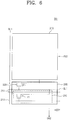
- FIG. 6 is a view showing a first pixel according to an embodiment of the present invention.
- a second gate circuit 210 according to the present embodiment includes only the first transistor T1, and the second transistor T2 (refer to FIG. 5 ) is disposed in the non-display part NDA (refer to FIG. 5 ) other than the first display part DA1 as a component of the first gate circuit 100.
- NDA non-display part
- the second gate circuit 210 may include only the second transistor T2 or may further include at least one of the buffer part 110, the charge part 120, the carry part 140, the first discharge part 151, the second discharge part 153, the switch part 170, the first maintain part 181, the second maintain part 182, the third maintain part 183, and the fourth maintain part 184.
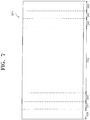
- FIG. 7 is a view showing a display panel DP1 according to an embodiment of the present invention.
- FIG. 7 shows only high-level representations of the first, second, and third display parts DA1 to DA3, and configuration details (e.g., the first and second circuits 100 and 200 shown in FIG. 1 ) of the first to third display parts DA1 to DA3 are omitted.
- each of the first and second display parts DA1 and DA2 of the display panel DP1 is provided in a plural number.
- the first, second, and third display parts DA1 to DA3 are arranged in the display panel DP1 in order of the first display part DA1, the second display part DA2, the third display part DA3, the second display part DA2, and the first display part DA1.
- the gate driver GD (refer to FIG. 1 ) is disposed in the non-display part NDA and the first display part DA1, which are defined at opposite sides of the third display part DA3, and thus the display panel DP1 may be stably operated.
- the third display part DA3 has a large area, a difference in brightness between the areas at opposite sides of the third display part DA3 may be prevented from occurring, and the display panel DP1 may be more stably operated.
- FIG. 8 is a view showing a display panel DP2 according to an embodiment of the present invention.
- FIG. 8 shows only high-level representations of the first, second, and third display parts DA1 to DA3, and configuration details (e.g., the first and second circuits 100 and 200 shown in FIG. 1 ) of the first to third display parts DA1 to DA3 are omitted.
- the third display part DA3 of the display panel DP2 shown in FIG. 8 may be provided in a plural number.
- the third display parts DA3 are arranged to be spaced apart from each other in the first direction DR1.
- the display panel DP2 includes the first, second, and third display parts DA1, DA2, and DA3 arranged in the first direction DR1 in order of the first display part DA1, the second display part DA2, the third display part DA3, the second display part DA2, the first display part DA1, the second display part DA2, the third display part DA3, the second display part DA2, and the first display part DA1.
- the third display part DA3 has a large area, a difference in brightness between the areas at opposite sides of the third display part DA3 may be prevented from occurring, and the display panel DP1 may be more stably operated.
- FIG. 9 is a view showing a display panel DP3 according to an embodiment of the present invention.
- the display panel DP3 includes a gate driver GF implemented by an in-pixel gate driver.
- the gate driver GF has the same structure and function as those of the gate driver GD shown in FIG. 1 except that the gate driver GF further includes third gate circuits 250, and thus repetitive explanations are omitted.
- the second gate circuits 210 are connected to corresponding third gate circuits 250 through the signal line SL.
- the second gate circuits 210 are arranged in a matrix form to correspond to the first pixels PX1.
- an i-th second gate circuit in the first direction DR1 among the second gate circuits 210 is disposed between an i-th data line and an (i+1)-th data line among the data lines DL1 to DLm.
- the third gate circuits 250 are arranged in a matrix form to correspond to the second pixels PX2.
- a third gate circuit in the first direction DR1 among the third gate circuits 250 is disposed between a j-th data line and a (j+1)-th data line among the data lines DL1 to DLm.
- the number "j" is an integer greater than the number "i”.
- a k-th third gate circuit in the second direction DR2 is disposed between a k-th gate line and a (k+1)-th gate line among the gate lines GL1 to GLn.
- a k-th stage is configured to include the first, second, and third gate circuits 100, 210, and 250 arranged in a k-th row.
- the first, second, and third gate circuits 100, 210, and 250 arranged in the k-th row are connected to each other by the signal line SL.
- each of the first to n-th stages SG1 to SGn includes two third gate circuits 250, but the number of the third gate circuits 250 in each of the first to n-th stages SG1 to SGn is not limited to two. That is, each of the first to n-th stages SG1 to SGn may include q or more third gate circuits 250. The number "q" is determined depending on characteristics of each of the gate lines GL1 to GLn.
- the gate driver GF Since several configurations of the gate driver GF are spatially distributed in the first and second display parts DA1 and DA2 as the third gate circuit 250, the width of the non-display part NDA (or bezel) is effectively reduced, and the transmittance of the first display part DA1 is improved.
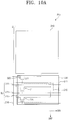
- FIG. 10A is a view showing the first pixel PX1 shown in FIG. 9 according to an embodiment of the present invention
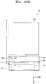
- FIG. 10B is a view showing the second pixel PX2 shown in FIG. 9 according to an embodiment of the present invention
- FIG. 10C is a view showing the third pixel PX3 shown in FIG. 9 according to an embodiment of the present invention.
- the first and third pixels PX1 and PX3 shown in FIGS. 10A and 10C are substantially the same as the first and third pixels PX1 and PX3 shown in FIGS. 2A and 2C , and thus details thereof are omitted.
- the second pixel PX2 includes the second pixel electrode 410, the second pixel circuit 420, and a second light blocking part 440.
- the third gate circuit 250 is disposed spaced apart from the second pixel electrode 410 in the second direction DR2.
- the second transistor may be provided in a plural number. Accordingly, as shown in FIG. 10A , at least one transistor T21 of the second transistors is disposed in the second gate circuit 210, and at least one transistor T22 of the third transistors is disposed in the third gate circuit 250.
- each of the off-switching line 216 and the low voltage line 215 may be disposed in the second display part DA2.
- at least the portion of each of the off-switching line 216 and the low voltage line 215 may be overlapped with the second light blocking part 440 when viewed in a plan view.
- the second light blocking part 440 prevents the second pixel circuit 420, the third gate circuit 250, and the first gate line GL1 from being visible.
- the second light blocking part 440 is overlapped with the second pixel circuit 420, the third gate circuit 250, and the first gate line GL1 when viewed in a plan view.
- the third gate circuit 250 is not limited thereto or thereby.
- an area in which the third gate circuit 250 is disposed may be smaller than an area in which the second gate circuit 210 is disposed, or the number of the transistors included in the third gate circuit 250 may be smaller than the number of the transistors included in the second gate circuit 210.
- a relationship of N1>N2 or R1>R2 may be satisfied.
- the N1 denotes the number of transistors of the second gate circuit 210
- the N2 denotes the number of transistors of the third gate circuit 250
- the R1 denotes the area in which the second gate circuit 210 is disposed
- the R2 denotes the area in which the third gate circuit 250 is disposed.
- the third gate circuit 250 may include the first transistor T1 instead of the second transistor T22.
- FIG. 11 is a view showing a first pixel PX1 shown in FIG. 9 according to an embodiment of the present invention.
- the second gate circuit 210 may include the first transistor T1 and may not include the second transistor T2.
- each of the on-switching line 213, the low voltage line 215 and the off-switching line 216 may be disposed in the first display part DA1.
- at least a portion of each of the on-switching line 213, the off-switching line 216 and the low voltage line 215 may be overlapped with the first light blocking part 331.
- the first light blocking part 331 prevents the first switching transistor ST1, the second gate circuit 210, and the first gate line GL1 from being visible.
- the first light blocking part 331 is overlapped with the first switching transistor ST1, the second gate circuit 210, and the first gate line GL1 when viewed in a plan view.
- FIG. 12 is a view showing a display apparatus 1000 according to an embodiment of the present.
- the display apparatus 1000 may further include a backlight unit BLU, and a display panel DP may be, but not limited to, a liquid crystal display panel.
- the backlight unit BLU may include, for example, first, second, and third parts P1, P2, and P3.
- the first to third parts P1 to P3 are respectively overlapped with the first to third display parts DA1 to DA3 in a plan view.
- the first, second, and third parts P1, P2, and P3 respectively generate first, second, and third lights L1, L2, and L3, and the first to third lights L1 to L3 are provided to rear surfaces of the first to third display parts DA1 to DA3, respectively.
- an intensity of the first to third lights L1 to L3 may be controlled according to the transmittance of the first to third display parts DA1 to DA3.
- the intensity of the second light L2 may be smaller than the intensity of the first light L1 and greater than the intensity of the third light L3.
- a ratio of intensity among the first to third lights L1 to L3 may be substantially the same as a ratio of the first to third transmittances or a ratio of squares of the first to third transmittances.
- the ratio of intensity among the first to third lights L1 to L3 may be substantially the same as a ratio of area among the first, second, and third light blocking parts 330, 430, and 530 (refer to FIGS. 3A to 3C ) or a ratio of squares of the areas of the first, second, and third light blocking parts 330, 430, and 530.
- the light having a relatively high intensity is provided to the part of the display panel DP having a relatively low transmittance, and thus the boundary between the first and third display parts DA1 and DA3 may be prevented from being recognized due to the difference in transmittance between the first and third display parts DA1 and DA3.
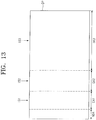
- FIG. 13 is a view showing a display panel according to an embodiment of the present invention.
- first, second, and third image signals IS1, IS2, and IS3 are respectively applied to the first, second, and third display parts DA1, DA2, and DA3.
- the first to third image signals IS1 to IS3 may be signals having information on images displayed through the first to third display parts DA1 to DA3.
- the first to third image signals IS1 to IS3 may be external signals provided from the outside, processed signals in the controller CTR, which are obtained by processing the external signals to be suitable for the display panel DP, or the data voltages generated on the basis of the external signals or the processed signals.
- a brightness value of the second image signal IS2 is smaller than a brightness value of the first image signal IS1 and greater than a brightness value of the third image signal IS3 when a grayscale value is constant.
- a ratio in brightness value among the first to third image signals IS1 to IS3 may be substantially the same as a ratio of the first to third transmittances or a ratio of squares of the first to third transmittances.
- the ratio in brightness value among the first to third lights L1 to L3 may be substantially the same as a ratio in area among the first, second, and third light blocking parts 330, 430, and 530 (refer to FIGS. 3A to 3C ) or a ratio of squares of the areas of the first, second, and third light blocking parts 330, 430, and 530.
- the image signal having a relatively high brightness value at the same grayscale value is provided to the part of the display panel DP having a relatively low transmittance, and thus the boundary between the first and third display parts DA1 and DA3 may be prevented from being recognized due to the difference in transmittance between the first and third display parts DA1 and DA3.
Landscapes
- Physics & Mathematics (AREA)
- Engineering & Computer Science (AREA)
- General Physics & Mathematics (AREA)
- Nonlinear Science (AREA)
- Chemical & Material Sciences (AREA)
- Crystallography & Structural Chemistry (AREA)
- Computer Hardware Design (AREA)
- Theoretical Computer Science (AREA)
- Optics & Photonics (AREA)
- Mathematical Physics (AREA)
- Microelectronics & Electronic Packaging (AREA)
- Devices For Indicating Variable Information By Combining Individual Elements (AREA)
- Liquid Crystal (AREA)
- Liquid Crystal Display Device Control (AREA)
- Control Of Indicators Other Than Cathode Ray Tubes (AREA)
- Electroluminescent Light Sources (AREA)
Abstract
Description
- The present invention relates to a display apparatus having a narrow bezel.
- A flat display panel is typically classified into a light-emitting type and a light-receiving type. The light-emitting type of flat display panel includes, for example, a plasma display panel and an organic light emitting display panel.
- The flat panel display panel includes a plurality of pixels and a gate driver driving the pixels. In general, the gate driver is disposed in a non-display region adjacent to a display region in which the pixels are arranged. The display panel has a bezel width corresponding to the non-display region.
- The present invention sets out to provide a display apparatus having a narrow bezel width.
- Embodiments of the inventive concept provide a display apparatus including a display panel including a gate line extending in one direction, a non-display part, a first display part, a third display part, and a second display part disposed between the first and third display parts and a gate driver including a first gate circuit disposed in the non-display part and a second gate circuit disposed in the first display part and applying a gate signal to the gate line. The first display part includes a first pixel including a first pixel electrode, a first pixel circuit driving the first pixel electrode, and a first light blocking part overlapped with the first pixel circuit and the second gate circuit, the second display part includes a second pixel including a second pixel electrode, a second pixel circuit driving the second pixel electrode, and a second light blocking part overlapped with the second pixel circuit, the third display part includes a third pixel including a third pixel electrode, a third pixel circuit driving the third pixel electrode, and a third light blocking part overlapped with the third pixel circuit, and an area of the second light blocking part is smaller than an area of the first light blocking part and greater than an area of the third light blocking part.
- The gate line may be provided in a plural number, and the second gate circuit may be disposed between adjacent gate lines to each other among the gate lines.
- The second gate circuit may include a first transistor including an input terminal connected to a clock line and an output terminal connected to the gate line.
- The second gate circuit may further include a second transistor including an input terminal connected to a low voltage line and an output terminal connected to the output terminal of the first transistor.
- The second pixel electrode may have an area greater than an area of the first pixel electrode and smaller than an area of the third pixel electrode.
- The gate driver may further include a third gate circuit disposed in the second display part, and the second light blocking part may be overlapped with the third gate circuit.
- An area in which the third gate circuit is disposed is smaller than an area in which the second gate circuit is disposed.
- The number of transistors included in the third gate circuit may be smaller than the number of transistors included in the second gate circuit.
- The display panel may further include a clock line receiving a clock signal and a low voltage line receiving a low voltage, the gate driver may further include a plurality of second transistors, each of the second transistors may include an input terminal connected to the low voltage line and an output terminal connected to the gate line, the second gate circuit may include a first transistor including an input terminal connected to the clock line and an output terminal connected to the gate line, and the third gate circuit may include at least one second transistor among the second transistors.
- At least a portion of the low voltage line and at least a portion of the clock line may be disposed in the first and second display parts.
- The second gate circuit may include at least another second transistor among the second transistors.
- The display panel may further include a plurality of data lines extending in another direction different from the one direction, the second gate circuit may be provided in a plural number, an i-th second gate circuit in the one direction among the second gate circuits may be disposed between an i-th data line and an (i+1)-th data line among the data lines, and the number "i" may be an integer equal to or greater than 1.
- The third gate circuit may be provided in a plural number, a third gate circuit in the one direction among the third gate circuits may be disposed between a j-th data line and a (j+1)-th data line among the data lines, and the number "j" may be an integer greater than the number "i".
- The gate line may be provided in a plural number, a k-th second gate circuit in the another direction different from the one direction among the second gate circuits may be disposed between a k-th gate line and a (k+1)-th gate line among the gate lines, and the number "k" may be an integer greater than 1.
- Each of the first display part and the second display part may be provided in a plural number, and the first display parts, the second display parts, and the third display part may be arranged in order of the first display part, the second display part, the third display part, the second display part, and the first display part along the one direction.
- Each of the first, second, and third display parts may be provided in a plural number, and the first, second, and third display parts may be arranged in order of the first display part, the second display part, the third display part, the second display part, the first display part, the second display part, the third display part, the second display part, and the first display part along the one direction.
- The display apparatus may further include a backlight unit configured to include a first part providing a first light to the first display part, a second part providing a second light to the second display part, and a third part providing a third light to the third display part. The second light may have an intensity smaller than an intensity of the first light and greater than an intensity of the third light.
- First, second, and third image signals may be respectively applied to the first, second, and third display parts, and the second image signal may have a brightness value smaller than a brightness value of the first image signal and greater than a brightness value of the third image signal with respect to a same grayscale value.
- Embodiments of the inventive concept may provide a display apparatus including a display panel including a gate line extending in one direction, a non-display part, a first display part, a third display part, and a second display part disposed between the first and third display parts and a gate driver including a first gate circuit disposed in the non-display part and a second gate circuit disposed in the first display part. The gate driver may be not disposed in the third display part and apply a gate signal to the gate line, and the second display part may have a transmittance greater than a transmittance of the first display part and smaller than a transmittance of the third display part.
- Embodiments of the inventive further concept provide a display apparatus including a display panel including a gate line extending in one direction, a first display part, a third display part, and a second display part disposed between the first and third display parts and a gate driver including a first gate circuit disposed in the first display part and a second gate circuit disposed in the second display part. The gate driver is not disposed in the third display part and applies a gate signal to the gate line. A relationship of N1>N2 or R1>R2 is satisfied, the number N1 denotes a number of transistors of the first gate circuit, the number N2 denotes a number of transistors of the second gate circuit, the number R1 denotes an area in which the first gate circuit is disposed, and the number R2 denotes an area in which the
second gate circuit 250 is disposed. - Embodiments of the inventive further concept provide a display apparatus including a display panel including a gate line extending in one direction, a non-display part, a first display part, a third display part, a second display part disposed between the first and third display parts, and a gate driver comprising a first gate circuit disposed in the non-display part and a second gate circuit disposed in the first display part. The gate driver is not disposed in the third display part and applies a gate signal to the gate line. The first display part comprises a first pixel of a first type, the second display part comprises a second pixel of a second type, the third display part comprises a third pixel of a third type, and an aperture ratio of the second pixel is greater than an aperture ratio of the first pixel and smaller than an aperture ratio of the third pixel.
- Each pixel may have a light blocking part and a display area that is not overlapped with the light blocking part, and the aperture ratio of each pixel may be a ratio of the display area and the area of the light block part.
- Each pixel column may contain pixels of the same pixel type. One or more contiguous columns of pixels of the first type may form the first display part, one or more contiguous columns of pixels of the second type may form the second display part, and one or more contiguous columns of pixels of the third type may form the third display part.
- The display panel may be apportioned into a plurality of display parts along a pixel row direction, and the plurality of display parts may be arranged in order of the first display part, the second display part, the third display part, the second display part, and the first display part along the pixel row direction.
- The display panel may be apportioned into a plurality of display parts along a pixel row direction, and the plurality of display parts may be arranged in order of the first display part, the second display part, the third display part, the second display part, the first display part, the second display part, the third display part, the second display part, and the first display part along the pixel row direction.
- At least some of the above and other features of the invention are set out in the claims.
- According to the above, the second gate circuit of the gate driver is disposed in the first display part, and thus the bezel width of the display apparatus may be reduced.
- The area of the second light blocking part is smaller than the area of the first light blocking part and greater than the area of the third light blocking part. Accordingly, the boundary between the first and third display parts may be prevented from being recognized, which is caused by the difference in transmittance between the first and third display parts when the second gate circuit is disposed in the first display part. As a result, the display quality of the display apparatus may be improved.
- The above and other advantages of the present disclosure will become readily apparent by reference to the following detailed description when considered in conjunction with the accompanying drawings wherein:
-
FIG. 1 is a plan view showing a display apparatus according to an embodiment of the present invention; -
FIG. 2A is a view showing a first pixel shown inFIG. 1 ; -
FIG. 2B is a view showing a second pixel shown inFIG. 1 ; -
FIG. 2C is a view showing a third pixel shown inFIG. 1 ; -
FIG. 3A is a layout of the pixel shown inFIG. 2A ; -
FIG. 3B is a layout of the pixel shown inFIG. 2B ; -
FIG. 3C is a layout of the pixel shown inFIG. 2C ; -
FIG. 4 is a cross-sectional view taken along a line I-I' ofFIG. 3A ; -
FIG. 5 is a circuit diagram showing a first stage shown inFIG. 1 ; -
FIG. 6 is a view showing a first pixel according to an embodiment of the present invention; -
FIG. 7 is a view showing a display panel according to an embodiment of the present invention; -
FIG. 8 is a view showing a display panel according to an embodiment of the present invention; -
FIG. 9 is a view showing a display panel according to an embodiment of the present invention; -
FIG. 10A is a view showing a first pixel shown inFIG. 9 according to an embodiment of the present invention; -
FIG. 10B is a view showing a second pixel shown inFIG. 9 according to an embodiment of the present invention; -
FIG. 10C is a view showing a third pixel shown inFIG. 9 according to an embodiment of the present invention; -
FIG. 11 is a view showing a first pixel shown inFIG. 9 according to an embodiment of the present invention; -
FIG. 12 is a view showing a display apparatus according to an embodiment of the present invention; and -
FIG. 13 is a view showing a display panel according to an embodiment of the present invention. - The following description with reference to the accompanying drawings is provided to assist in a comprehensive understanding of various embodiments of the present invention as defined by the claims. It includes various specific details to assist in that understanding, but these details are to be regarded as mere examples. Accordingly, those of ordinary skill in the art would recognize that various changes and modifications of the various embodiments described herein can be made without departing from the scope of the claims. Like numbers refer to like elements throughout.
- Hereinafter, the present invention is explained in detail with reference to the accompanying drawings.
-
FIG. 1 is a plan view showing adisplay apparatus 1000 according to an exemplary embodiment of the present invention. - Referring to
FIG. 1 , thedisplay apparatus 1000 includes a display panel DP displaying an image and a panel driver driving the display panel DP. The panel driver includes a gate driver GD, a data driver DD, and a controller CTR controlling the gate driver GD and the data driver DD. - The controller CTR receives a plurality of control signals CS and input image data RGB containing information on the image. The controller CTR converts the input image data RGB to output image data RGB' appropriate to an interface between the data driver DD and the display panel DP and applies the output image data RGB' to the data driver DD. In addition, the controller CTR generates a data control signal D-CS (e.g., an output start signal, a horizontal start signal, etc.) and a gate control signal G-CS on the basis of the control signals CS. The data control signal D-CS is applied to the data driver DD, and the gate control signal G-CS is applied to the gate driver GD.
- The gate driver GD sequentially outputs gate signals in response to the gate control signal G-CS provided from the controller CTR.
- The data driver DD converts the output image data RGB' to data voltages in response to the data control signal D-CS provided from the controller CTR and outputs the data voltages. The data voltages are applied to the display panel DP.
- The display panel DP includes a plurality of gate lines GL1 to GLn, a plurality of data lines DL1 to DLm (where n and m are natural numbers), signal lines SL, and a plurality of pixels. The display panel DP may be, but not limited to, a flat display panel, such as an organic light emitting display panel including an organic light emitting layer or a liquid crystal display panel including a liquid crystal layer. The gate lines GL1 to GLn extend in a first direction DR1 and are arranged in a second direction DR2 to be substantially parallel to each other. The data lines DL1 to DLm are insulated from the gate lines GL1 to GLn that cross the data lines DL1 to DLm. For instance, the data lines DL1 to DLm extend in the second direction DR2 and are arranged in the first direction DR1 to be substantially parallel to each other. The first direction DR1 may be substantially perpendicular to the second direction DR2. In the following descriptions, the first and second directions DR1 and DR2 may be respectively referred to as one direction and the other direction.
- Each of the pixels displays one of three primary colors of red, green, and blue colors. The colors displayed by the pixels are not limited thereto or thereby, and the pixels may further display various colors, e.g., yellow, cyan, and magenta colors, in addition to the red, green, and blue colors. The pixels are arranged in a matrix form along the first and second directions DR1 and DR2.
- Each of the pixels is connected to a corresponding data line of the data lines DL1 to DLm and a corresponding gate line of the gate lines GL1 to GLn.
- In the present embodiment, the display panel DP includes a non-display part NDA and a display part. The display part displays the image, and the non-display part NDA does not display the image. The pixels are disposed in the display part. The pixels are not disposed in the non-display part NDA, and a circuit used to drive the pixels is disposed in the non-display part NDA.
- The display part includes first, second, and third display parts DA1, DA2, and DA3. The second display part DA2 is disposed between the first and third display parts DA1 and DA3. The non-display part NDA is disposed at a left end of the display panel DP.
- As an example, the parts may be arranged in order of "the non-display part NDA/the first display part DA1/the second display part DA2/the third display part DA3" in the first direction DR1.
- As an example, the pixels include first, second, and third pixels PX1, PX2, and PX3. The first to third display parts DA1 to DA3 include the first to third pixels PX1 to PX3, respectively.
- As an example, the gate driver GD may be implemented by "in-pixel gate driver". Accordingly, at least a portion of the gate driver GD may be disposed in the part in which the pixels are disposed. As an example, the gate driver GD includes a
first gate circuit 100 disposed in the non-display part NDA and asecond gate circuit 200 disposed in the first display part DA1. Each of the first andsecond gate circuits - The
first gate circuits 100 are arranged in the second direction DR2 to respectively correspond to the gate lines GL1 to GLn. - The
second gate circuits 200 are arranged in a matrix form to correspond to the first pixels PX1. In more detail, an i-th second gate circuit in the first direction DR1 among thesecond gate circuits 200 is disposed between an i-th data line and an (i+1)-th data line among the data lines DL1 to DLm, and a k-th second gate circuit in the second direction DR2 among thesecond gate circuits 200 is disposed between a k-th gate line and a (k+1)-th gate line among the gate lines GL1 to GLn. Each of "i" and "k" is an integer number equal to or greater than 1, with i < m and k < n. - The display panel DP includes first to n-th stages SG1 to SGn connected to each other in series. An k-th stage may be configured to include the first and
second gate circuits second gate circuits - In the present embodiment, each of the first to n-th stages SG1 to SGn includes two
second gate circuits 200, but it is not limited thereto or thereby. That is, each of the first to n-th stages SG1 to SGn may include q or moresecond gate circuits 200. The number "q" is an integer equal to or greater than 3. - The number "q" is determined depending on a characteristic of each of the gate lines GL1 to GLn. The characteristic of each of the gate lines GL1 to GLn may be, but not limited to, an impedance characteristic. For instance, as the impedance of the gate lines GL1 to GLn increases, the number "q" increases.
- If the gate driver GD is implemented by the in-pixel gate driver, the
second gate circuits 200 are distributed and arranged in the first display part DA1, and thus, an area in which thesecond gate circuits 200 are disposed is not required. Thus, a width of the non-display part NDA, i.e., a bezel width, may be reduced. -
FIG. 2A is a view showing the first pixel PX1 shown inFIG. 1 ,FIG. 2B is a view showing the second pixel PX2 shown inFIG. 1 , andFIG. 2C is a view showing the third pixel PX3 shown inFIG. 1 . - Referring to
FIG. 2A , the first pixel PX1 includes afirst pixel electrode 310, afirst pixel circuit 320, and a firstlight blocking part 330. - The
first pixel electrode 310 may be, for example, a transmissive electrode or a reflective electrode. - In the present embodiment, the
first pixel circuit 320 is connected to the first gate line GL1 and the first data line DL1 to drive thefirst pixel electrode 310. Thefirst pixel circuit 320 includes a first switching transistor ST1. The first switching transistor ST1 includes an input terminal connected to the first data line DL1, a control terminal connected to the first gate line GL1, and an output terminal connected to thefirst pixel electrode 310. However, thefirst pixel circuit 320 may include two or more transistors, may be further connected to other lines in addition to the data line and the gate line, and may be implemented in various ways. - The first
light blocking part 330 is disposed to overlap with thesecond gate circuit 200 when viewed in a plan view such that at least thesecond gate circuit 200 is not visible. - The
second gate circuit 200 is disposed spaced apart from thefirst pixel electrode 310 in the second direction DR2. Thesecond gate circuit 200 includes the signal line SL, a first transistor T1, and a second transistor T2. In the present embodiment, the signal line SL includes an on-switchingline 213, an off-switchingline 216, alow voltage line 215, and aclock line 211. In the present embodiment, at least a portion of each of the on-switchingline 213, the off-switchingline 216, thelow voltage line 215, and theclock line 211 is overlapped with the firstlight blocking part 330 when viewed in a plan view. The first transistor T1 applies the first gate signal of high voltage to the first gate line GL1. An input terminal of the first transistor T1 is connected to theclock line 211 to receive a first clock signal from theclock line 211. A control terminal of the first transistor T1 is connected to the on-switchingline 213 to receive a Q-node signal from the on-switchingline 213. An output terminal of the first transistor T1 is connected to the first gate line GL1. - The second transistor T2 applies the first gate line of low voltage to the first gate line GL1. An input terminal of the second transistor T2 is connected to the
low voltage line 215 to receive the low voltage from thelow voltage line 215. A control terminal of the second transistor T2 is connected to the off-switchingline 216. The control terminal of the second transistor T2 receives a second gate signal of the second gate line GL2 (shown inFIG. 1 ) from the off-switchingline 216. An output terminal of the second transistor T2 is connected to the output terminal of the first transistor T1. - The first transistor T1 outputs the high voltage of the first clock signal to the first gate line GL1 as the high voltage of the gate voltage in response to the Q-node signal, and the second transistor T2 outputs the low voltage to the first gate line GL1 as the low voltage of the gate voltage in response to the second gate signal of the second gate line GL2 after a predetermined time lapses. The first switching transistor ST1 is turned on in response to the high voltage and applies the data voltage from the first data line DL1 to the
first pixel electrode 310. The first switching transistor ST1 may be turned off in response to the low voltage. - Referring to
FIG. 2B , the second pixel PX2 includes asecond pixel electrode 410, asecond pixel circuit 420, and a secondlight blocking part 430. - The
second pixel electrode 410 may be, for example, a transmissive electrode or a reflective electrode. - In the present embodiment, the
second pixel circuit 420 is connected to the first gate line GL1 and the second data line DL2 to drive thesecond pixel electrode 410. Thesecond pixel circuit 420 includes a second switching transistor ST2. The second switching transistor ST2 includes an input terminal connected to the second data line DL2, a control terminal connected to the first gate line GL1, and an output terminal connected to thesecond pixel electrode 410. - The second switching transistor ST2 receives the first gate signal from the first gate line GL1. The second switching transistor ST2 is turned on in response to the high voltage of the first gate signal and applies the data voltage provided from the second data line DL2 to the
second pixel electrode 410. The second switching transistor ST2 may be turned off in response to the low voltage of the first gate signal. - The second
light blocking part 430 is disposed to overlap with the second switching transistor ST2 when viewed in a plan view such that at least the second switching transistor ST2 is not visible. - Referring to
FIG. 2C , the third pixel PX3 includes athird pixel electrode 510, athird pixel circuit 520, and a thirdlight blocking part 530. - The
third pixel electrode 510 may be, for example, a transmissive electrode or a reflective electrode. - In the present embodiment, the
third pixel circuit 520 is connected to the first gate line GL1 and the third data line DL3 to drive thethird pixel electrode 510. Thethird pixel circuit 520 includes a third switching transistor ST3. The third switching transistor ST3 includes an input terminal connected to the third data line DL3, a control terminal connected to the first gate line GL1, and an output terminal connected to thethird pixel electrode 510. - The third switching transistor ST3 receives the first gate signal from the first gate line GL1. The third switching transistor ST3 is turned on in response to the high voltage of the first gate signal and applies the data voltage provided from the third data line DL3 to the
third pixel electrode 510. The third switching transistor ST3 may be turned off in response to the low voltage of the first gate signal. - The third
light blocking part 530 is disposed to overlap with the third switching transistor ST3 when viewed in a plan view such that at least the third switching transistor ST3 is not visible. -
FIG. 3A is a layout of the pixel shown inFIG. 2A ,FIG. 3B is a layout of the pixel shown inFIG. 2B ,FIG. 3C is a layout of the pixel shown inFIG. 2C , andFIG. 4 is a cross-sectional view taken along a line I-I' ofFIG. 3A . - Referring to
FIGS. 3A and4 , the first pixel PX1 includes thefirst pixel electrode 310, thefirst pixel circuit 320, and the firstlight blocking part 330. - The first switching transistor ST1 includes a first gate electrode GE1, a first active pattern AP1, a first source electrode SE1, and a first drain electrode DE1. In the following description, the gate electrode, the source electrode, and the drain electrode of the transistor may be respectively referred to as the control terminal, the input terminal, and the output terminal.
- The first gate electrode GE1 is branched from the first gate line GL1, and the first active pattern AP1 is disposed above the first gate electrode GE1 such that a first insulating layer IL1 is disposed between the first active pattern AP1 and the first gate electrode GE1. The first source electrode SE1 is branched to make contact with the first active pattern AP1, and the first drain electrode DE1 is spaced apart from the first source electrode SE1 to make contact with the first active pattern AP1.
- A second insulating layer IL2 covers the first switching transistor ST1. The
first pixel electrode 310 is disposed on the second insulating layer IL2, and thefirst pixel electrode 310 makes contact with the first drain electrode DE1 through a first contact hole CNT1 defined through the second insulating layer IL2. - The
lines - The first transistor T1 includes a second gate electrode GE2, a second active pattern AP2, a second source electrode SE2, and a second drain electrode DE2.
- The second gate electrode GE2 is branched from the on-switching
line 213, and the second active pattern AP2 is disposed above the second gate electrode GE2 such that the first insulating layer IL1 is disposed between the second active pattern AP2 and the second gate electrode GE2. - One end of the second source electrode SE2 makes contact with the second active pattern AP2, and the other end of the second source electrode SE2 makes contact with the
clock line 211 through a second contact hole CNT2 defined through the first insulating layer IL1. The one end of the second source electrode SE2 may include two first branch portions extending in a third direction DR3 opposite to the second direction DR2. - One end of the second drain electrode DE2 is spaced apart from the second source electrode SE2 and makes contact with the second active pattern AP2, and the other end of the second drain electrode DE2 is connected to the first gate line GL1 through a third contact hole CNT3 defined through the first insulating layer IL1. The second drain electrode DE2 includes two first recesses.
- The first recesses are recessed toward the third direction DR3. The two branch portions are respectively inserted into the two first recesses. Accordingly, the two first branch portions are overlapped with the two recesses in the first direction DR1. The number of the first branch portions and the number of the first recesses may be determined depending on the driving characteristic of the first transistor T1. For instance, three or more first branch portions and first recesses may be applied to the pixel to improve the driving characteristic, i.e., a driving capacity, or to increase a W/L ratio of a channel width of the first transistor T1 to a channel length of the first transistor T1.
- The second transistor T2 includes a third gate electrode GE3, a third active pattern AP3, a third source electrode SE3, and a third drain electrode DE3.
- The third gate electrode GE3 is branched from the off-switching
line 216, and the third active pattern AP3 is disposed above the third gate electrode GE3 such that the first insulating layer IL1 is disposed between the third active pattern AP3 and the third gate electrode GE3. - One end of the third source electrode SE3 makes contact with the third active pattern AP3, and the other end of the third source electrode SE3 makes contact with the
low voltage line 215 through a fourth contact hole CNT4 defined through the first insulating layer IL1. The one end of the third source electrode SE3 may include two second branch portions extending in the third direction DR3. - One end of the third drain electrode DE3 is spaced apart from the third source electrode SE3 and makes contact with the third active pattern AP3, and the other end of the third drain electrode DE3 is branched from the second drain electrode DE2. The third drain electrode DE3 includes two second recesses. The second branch portions and the second recesses have the similar structure and function as those of the first branch portions and the first recesses, and thus details thereof are omitted.
- The first
light blocking part 330 prevents the first switching transistor ST1, thesecond gate circuit 200, and the first gate line GL1 from being visible. The firstlight blocking part 330 is overlapped with the first switching transistor ST1, thesecond gate circuit 200, and the first gate line GL1 when viewed in a plan view. - In the present embodiment, the first
light blocking part 330 has a substantially quadrangular shape and has the same width as thefirst pixel electrode 310 in the first direction DR1. The firstlight blocking part 330 has a first width W1 in the second direction DR2. - In the present disclosure, a transmittance of the display panel DP at an arbitrarily selected area or portion may be defined by a ratio of an area covered by a light blocking part, e.g., the first
light blocking part 330, to an area not covered by firstlight blocking part 330. - The first
light blocking part 330 is interposed between an upper base substrate US of the display panel DP and a common electrode CE and includes a black matrix containing a light absorbing material. However, the firstlight blocking part 330 is not limited thereto or thereby, and the firstlight blocking part 330 may have various shapes. That is, the first light blocking part may include a black matrix disposed between a lower base substrate LS of the display panel DP and a liquid crystal LL. In addition, the firstlight blocking part 330 may include a metal material having high reflectance or may have a color filter stack structure in which color filters transmitting different colors are stacked. The color filter may be stacked in a structure in which two color filters among a red color filter, a green color filter, and a blue color filter are stacked. - Referring to
FIG. 3B , the second pixel PX2 includes thesecond pixel electrode 410, thesecond pixel circuit 420, and the secondlight blocking part 430. - The
second pixel circuit 420 and thesecond pixel electrode 410 are respectively similar to thefirst pixel circuit 320 and thefirst pixel electrode 310, and thus details thereof are omitted. - In the present embodiment, the second
light blocking part 430 prevents thesecond pixel circuit 420 and the first gate line GL1 from being visible. The secondlight blocking part 430 is overlapped with thesecond pixel circuit 420 and the first gate line GL1 when viewed in a plan view. - In the present embodiment, the second
light blocking part 430 has a substantially quadrangular shape and has the same width in the first direction DR1 as thesecond pixel electrode 410. The secondlight blocking part 430 has a second width W2 in the second direction DR2. - In the present embodiment, the second
light blocking part 430 may include the same material as that of the firstlight blocking part 330. - Referring to
FIG. 3C , the third pixel PX3 includes thethird pixel electrode 510, thethird pixel circuit 520, and the thirdlight blocking part 530. - The
third pixel circuit 520 and thethird pixel electrode 510 are respectively similar to thefirst pixel circuit 320 and thefirst pixel electrode 310, and thus details thereof are omitted. - The third
light blocking part 530 prevents thethird pixel circuit 520 and the first gate line GL1 from being visible. The thirdlight blocking part 530 is overlapped with thethird pixel circuit 520 and the first gate line GL1 when viewed in a plan view. - In the present embodiment, the third
light blocking part 530 has a substantially quadrangular shape and has the same width in the first direction DR1 as thethird pixel electrode 510. The thirdlight blocking part 530 has a third width W3 in the second direction DR2. - In the present embodiment, the third
light blocking part 530 may include the same material as that of the firstlight blocking part 330. - Referring to
FIGS. 3A to 3C , the first, second, and thirdlight blocking parts light blocking parts third pixel electrodes - Consequently, a first transmittance of the first display part DA1 in which the first pixel PX1 is disposed is lowest, a third transmittance of the third display part DA3 in which the third pixel PX3 is disposed is highest, and a second transmittance of the second display part DA2 in which the second pixel PX2 is disposed has a value between the first and third transmittances.
- That is, since the
second gate circuit 200 is disposed in the first display part DA1, a large difference exists between the first and third transmittances. However, when the second display part DA2 having the second transmittance is interposed between the first and third display parts DA1 and DA3, a boundary between the first and third display parts DA1 and DA3 may be prevented from being recognized even though the difference in transmittance exists between the first and third display parts DA1 and DA3. That is, the second display part makes the visual transition between the first and third transmittances less abrupt and less recognizable by a viewer of the display apparatus. As a result, a display quality of the display apparatus 1000 (refer toFIG. 1 ) may be improved. -
FIG. 5 is a circuit diagram showing a first stage shown inFIG. 1 . - Referring to
FIGS. 1 and5 , a control line CL and thefirst gate circuit 100 of the first stage SG1 are disposed in the non-display part NDA, and thesecond gate circuit 200 is disposed in the first display part DA1. - The control line CL includes a first voltage line VSL1, a first clock line CLK1, a second clock line CLK2, and a vertical start line STL, which are provided to the first stage SG1. Although not shown in figures, the control line CL may further include a third clock line and a fourth clock line. The first voltage line VSL1 transmits the low voltage, the first clock line CLK1 transmits the first clock signal, the second clock line CLK2 transmits the second clock signal, and the vertical start line STL transmits the vertical start signal.
- In the present embodiment, the
first gate circuit 100 includes abuffer part 110, acharge part 120, acarry part 140, afirst discharge part 151, asecond discharge part 153, aswitch part 170, a first maintainpart 181, a second maintainpart 182, a third maintainpart 183, and a fourth maintainpart 184. - The
buffer part 110 includes a fourth transistor T4. A control terminal and an input terminal of thebuffer part 110 are connected to the vertical start line STL to receive the vertical start signal, and an output terminal of thebuffer part 110 is connected to the Q-node Q (or control node). Responsive to the high voltage of the vertical start signal, thebuffer part 110 allows thecharge part 120 connected to the Q-node Q to be charged with the high voltage of the vertical start signal. - The
charge part 120 includes a boost capacitor Cgs. The boost capacitor Cgs includes a first terminal connected to the Q-node Q and a second terminal connected to the first gate line GL1. - The control terminal of the first transistor T1 is electrically connected to the first terminal of the
charge part 120 connected to the Q-node Q through the on-switchingline 213, the input terminal of the first transistor T1 receives the first clock signal through theclock line 211 connected to the first clock line CLK1, and the output terminal is connected to the first gate line GL1. When the first clock signal is received while the high voltage charged in the boost capacitor Cgs is applied to the control terminal of the first transistor T1, the first transistor T1 is bootstrapped. In this case, the boost capacitor Cgs boosts the voltage charged therein. The first transistor T1 applies the high voltage of the first clock signal to the first gate line GL1 in response to the boosted voltage. - The
carry part 140 includes a fifteenth transistor T15. A control terminal of thecarry part 140 is connected to the Q-node Q, an input terminal of thecarry part 140 receives the first clock signal, and an output terminal of thecarry part 140 is connected to one stage among the next stages following thecarry part 140. When the high voltage is applied to the Q-node Q, thecarry part 140 applies the high voltage of the first clock signal to the second stage SG2 as a first carry signal CR1. - The
discharge part 151 includes a ninth transistor T9. A control terminal of thedischarge part 151 is connected to the off-switchingline 216 and receives therefrom a second gate signal of the second gate line GL2 from the second stage SG2 (refer toFIG. 1 ) corresponding to one of the next stages, an input terminal of thedischarge part 151 is connected to the Q-node Q, and an output terminal of thedischarge part 151 is connected to the first voltage line VSL1. Thefirst discharge part 151 discharges the voltage applied to the Q-node Q to the low voltage in response to the high voltage of the second gate signal output from the second stage SG2. - The control terminal of the second transistor T2 is connected to the second stage SG2 through the off-switching
line 216, the output terminal of the second transistor T2 is connected to the first gate line GL1, and the input terminal of the second transistor T2 is connected to the first voltage line VSL1 through thelow voltage line 215. The second transistor T2 discharges the voltage applied to the first gate line GL1 to the low voltage. - The
second discharge part 153 includes a sixth transistor T6. A control terminal of thesecond discharge part 153 receives a reset signal RS, an input terminal of thesecond discharge part 153 is connected to the Q-node Q, and an output terminal of thesecond discharge part 153 is connected to the first voltage line VSL1. Thesecond discharge part 153 discharges the voltage applied to the Q-node Q to the low voltage in response to the high voltage of the reset signal RS output from the n-th stage SGn corresponding to a final stage of the gate driver GD (refer toFIG. 1 ). - The
switch part 170 includes a twelfth transistor T12, a seventh transistor T7, a thirteenth transistor T13, and an eighth transistor T8. When the high voltage is applied to the first gate line GL1, the eighth and thirteenth transistors T8 and T13 are turned on, and a voltage applied to an N-node N is discharged to the low voltage. When the low voltage is applied to the first gate line GL1, the eighth and thirteenth transistors T8 and T13 are turned off, and thus a signal synchronized with the first clock signal is applied to the N-node N. - The first maintain
part 181 includes a tenth transistor T10. A control terminal of the first maintainpart 181 receives the first clock signal from the first clock line CK1, an input terminal of the first maintainpart 181 is connected to the Q-node Q, and an output terminal of the first maintainpart 181 is connected to the first gate line GL1. The first maintainpart 181 maintains the voltage of the Q-node Q to the voltage of the first gate line GL1 in response to the high voltage of the first clock signal. - The second maintain
part 182 includes a third transistor T3. A control terminal of the second maintainpart 182 is connected to the N-node N, an input terminal of the second maintainpart 182 is connected to the first gate line GL1, and an output terminal of the second maintainpart 182 is connected to the first voltage line VSL1. - The second maintain
part 182 maintains the voltage of the first gate line GL1 to the low voltage in response to the high voltage applied to the N-node N. The third maintainpart 183 includes an eleventh transistor T11. A control terminal of the third maintainpart 183 is connected to the second clock line CLK2 to receive the second clock signal, an input terminal of the third maintainpart 183 receives the vertical start signal, and an output terminal of the third maintainpart 183 is connected to the Q-node Q. The third maintainpart 183 maintains the voltage of the Q-node Q to the voltage level of the vertical start signal in response to the high voltage of the second clock signal. The fourth maintainpart 184 includes a fifth transistor T5. A control terminal of the fourth maintainpart 184 receives the second clock signal, an input terminal of the fourth maintainpart 184 is connected to the first gate line GL1, and an output terminal of the fourth maintainpart 184 is connected to the first voltage line VSL1. The fourth maintainpart 184 maintains the voltage of the first gate line GL1 to the low voltage in response to the high voltage of the second clock signal. - According to the above-mentioned description, the first and second transistors T1 and T2 are disposed in the first display part DA1 as components of the
second gate circuit 200, but the present disclosure is not thereto or thereby. -
FIG. 6 is a view showing a first pixel according to an embodiment of the present invention. As shown inFIG. 6 , asecond gate circuit 210 according to the present embodiment includes only the first transistor T1, and the second transistor T2 (refer toFIG. 5 ) is disposed in the non-display part NDA (refer toFIG. 5 ) other than the first display part DA1 as a component of thefirst gate circuit 100. Alternatively, although not shown inFIG. 6 , thesecond gate circuit 210 may include only the second transistor T2 or may further include at least one of thebuffer part 110, thecharge part 120, thecarry part 140, thefirst discharge part 151, thesecond discharge part 153, theswitch part 170, the first maintainpart 181, the second maintainpart 182, the third maintainpart 183, and the fourth maintainpart 184. -
FIG. 7 is a view showing a display panel DP1 according to an embodiment of the present invention.FIG. 7 shows only high-level representations of the first, second, and third display parts DA1 to DA3, and configuration details (e.g., the first andsecond circuits FIG. 1 ) of the first to third display parts DA1 to DA3 are omitted. - In the present embodiment, each of the first and second display parts DA1 and DA2 of the display panel DP1 is provided in a plural number. The first, second, and third display parts DA1 to DA3 are arranged in the display panel DP1 in order of the first display part DA1, the second display part DA2, the third display part DA3, the second display part DA2, and the first display part DA1.
- In the above-mentioned structure, the gate driver GD (refer to
FIG. 1 ) is disposed in the non-display part NDA and the first display part DA1, which are defined at opposite sides of the third display part DA3, and thus the display panel DP1 may be stably operated. In particular, although the third display part DA3 has a large area, a difference in brightness between the areas at opposite sides of the third display part DA3 may be prevented from occurring, and the display panel DP1 may be more stably operated. - The first to third display parts DA1 to DA3 are not limited thereto or thereby.
FIG. 8 is a view showing a display panel DP2 according to an embodiment of the present invention.FIG. 8 shows only high-level representations of the first, second, and third display parts DA1 to DA3, and configuration details (e.g., the first andsecond circuits FIG. 1 ) of the first to third display parts DA1 to DA3 are omitted. - Different from the display panel DP1 shown in
FIG. 7 , the third display part DA3 of the display panel DP2 shown inFIG. 8 may be provided in a plural number. The third display parts DA3 are arranged to be spaced apart from each other in the first direction DR1. The display panel DP2 includes the first, second, and third display parts DA1, DA2, and DA3 arranged in the first direction DR1 in order of the first display part DA1, the second display part DA2, the third display part DA3, the second display part DA2, the first display part DA1, the second display part DA2, the third display part DA3, the second display part DA2, and the first display part DA1. - Accordingly, although the third display part DA3 has a large area, a difference in brightness between the areas at opposite sides of the third display part DA3 may be prevented from occurring, and the display panel DP1 may be more stably operated.
-
FIG. 9 is a view showing a display panel DP3 according to an embodiment of the present invention. - Referring to
FIG. 9 , the display panel DP3 includes a gate driver GF implemented by an in-pixel gate driver. The gate driver GF has the same structure and function as those of the gate driver GD shown inFIG. 1 except that the gate driver GF further includesthird gate circuits 250, and thus repetitive explanations are omitted. - In addition, a different reference number has been assigned to the
second gate circuits 210 shown inFIG. 9 so as to distinguish thesecond gate circuits 210 from thesecond gate circuits 200 shown inFIG. 1 . Thesecond gate circuits 210 are connected to correspondingthird gate circuits 250 through the signal line SL. - The
second gate circuits 210 are arranged in a matrix form to correspond to the first pixels PX1. In more detail, an i-th second gate circuit in the first direction DR1 among thesecond gate circuits 210 is disposed between an i-th data line and an (i+1)-th data line among the data lines DL1 to DLm. - The
third gate circuits 250 are arranged in a matrix form to correspond to the second pixels PX2. In more detail, a third gate circuit in the first direction DR1 among thethird gate circuits 250 is disposed between a j-th data line and a (j+1)-th data line among the data lines DL1 to DLm. The number "j" is an integer greater than the number "i". - Among the
third gate circuits 250, a k-th third gate circuit in the second direction DR2 is disposed between a k-th gate line and a (k+1)-th gate line among the gate lines GL1 to GLn. - In the present embodiment, among the first to n-th stages SG1 to SGn, a k-th stage is configured to include the first, second, and
third gate circuits third gate circuits - In the present embodiment, each of the first to n-th stages SG1 to SGn includes two
third gate circuits 250, but the number of thethird gate circuits 250 in each of the first to n-th stages SG1 to SGn is not limited to two. That is, each of the first to n-th stages SG1 to SGn may include q or morethird gate circuits 250. The number "q" is determined depending on characteristics of each of the gate lines GL1 to GLn. - Since several configurations of the gate driver GF are spatially distributed in the first and second display parts DA1 and DA2 as the
third gate circuit 250, the width of the non-display part NDA (or bezel) is effectively reduced, and the transmittance of the first display part DA1 is improved. -
FIG. 10A is a view showing the first pixel PX1 shown inFIG. 9 according to an embodiment of the present invention,FIG. 10B is a view showing the second pixel PX2 shown inFIG. 9 according to an embodiment of the present invention, andFIG. 10C is a view showing the third pixel PX3 shown inFIG. 9 according to an embodiment of the present invention. - The first and third pixels PX1 and PX3 shown in
FIGS. 10A and10C are substantially the same as the first and third pixels PX1 and PX3 shown inFIGS. 2A and2C , and thus details thereof are omitted. - Referring to
FIG. 10B , the second pixel PX2 includes thesecond pixel electrode 410, thesecond pixel circuit 420, and a secondlight blocking part 440. - The
third gate circuit 250 is disposed spaced apart from thesecond pixel electrode 410 in the second direction DR2. As an example, the second transistor may be provided in a plural number. Accordingly, as shown inFIG. 10A , at least one transistor T21 of the second transistors is disposed in thesecond gate circuit 210, and at least one transistor T22 of the third transistors is disposed in thethird gate circuit 250. - In the present embodiment, at least a portion of each of the off-switching
line 216 and thelow voltage line 215 may be disposed in the second display part DA2. For instance, at least the portion of each of the off-switchingline 216 and thelow voltage line 215 may be overlapped with the secondlight blocking part 440 when viewed in a plan view. - In the present embodiment, the second
light blocking part 440 prevents thesecond pixel circuit 420, thethird gate circuit 250, and the first gate line GL1 from being visible. The secondlight blocking part 440 is overlapped with thesecond pixel circuit 420, thethird gate circuit 250, and the first gate line GL1 when viewed in a plan view. - The
third gate circuit 250 is not limited thereto or thereby. In the present embodiment, to achieve a second transmittance of the second display part DA2 that is higher than a first transmittance of the first display part DA1, an area in which thethird gate circuit 250 is disposed may be smaller than an area in which thesecond gate circuit 210 is disposed, or the number of the transistors included in thethird gate circuit 250 may be smaller than the number of the transistors included in thesecond gate circuit 210. In other words, a relationship of N1>N2 or R1>R2 may be satisfied. The N1 denotes the number of transistors of thesecond gate circuit 210, the N2 denotes the number of transistors of thethird gate circuit 250, the R1 denotes the area in which thesecond gate circuit 210 is disposed, and the R2 denotes the area in which thethird gate circuit 250 is disposed. In the present exemplary embodiment, thethird gate circuit 250 may include the first transistor T1 instead of the second transistor T22. -
FIG. 11 is a view showing a first pixel PX1 shown inFIG. 9 according to an embodiment of the present invention. - Referring to
FIG. 11 , thesecond gate circuit 210 may include the first transistor T1 and may not include the second transistor T2. - In the present embodiment, at least a portion of each of the on-switching
line 213, thelow voltage line 215 and the off-switchingline 216 may be disposed in the first display part DA1. For instance, at least a portion of each of the on-switchingline 213, the off-switchingline 216 and thelow voltage line 215 may be overlapped with the firstlight blocking part 331. - The first
light blocking part 331 prevents the first switching transistor ST1, thesecond gate circuit 210, and the first gate line GL1 from being visible. The firstlight blocking part 331 is overlapped with the first switching transistor ST1, thesecond gate circuit 210, and the first gate line GL1 when viewed in a plan view. -
FIG. 12 is a view showing adisplay apparatus 1000 according to an embodiment of the present. - Referring to
FIG. 12 , thedisplay apparatus 1000 may further include a backlight unit BLU, and a display panel DP may be, but not limited to, a liquid crystal display panel. - The backlight unit BLU may include, for example, first, second, and third parts P1, P2, and P3. The first to third parts P1 to P3 are respectively overlapped with the first to third display parts DA1 to DA3 in a plan view. The first, second, and third parts P1, P2, and P3 respectively generate first, second, and third lights L1, L2, and L3, and the first to third lights L1 to L3 are provided to rear surfaces of the first to third display parts DA1 to DA3, respectively.
- In the present embodiment, an intensity of the first to third lights L1 to L3 may be controlled according to the transmittance of the first to third display parts DA1 to DA3. In more detail, since the second transmittance of the second display part DA2 is greater than the first transmittance of the first display part DA1 and smaller than the third transmittance of the third display part DA3, the intensity of the second light L2 may be smaller than the intensity of the first light L1 and greater than the intensity of the third light L3.
- As an example, a ratio of intensity among the first to third lights L1 to L3 may be substantially the same as a ratio of the first to third transmittances or a ratio of squares of the first to third transmittances. In the present embodiment, the ratio of intensity among the first to third lights L1 to L3 may be substantially the same as a ratio of area among the first, second, and third
light blocking parts FIGS. 3A to 3C ) or a ratio of squares of the areas of the first, second, and thirdlight blocking parts - As described above, the light having a relatively high intensity is provided to the part of the display panel DP having a relatively low transmittance, and thus the boundary between the first and third display parts DA1 and DA3 may be prevented from being recognized due to the difference in transmittance between the first and third display parts DA1 and DA3.
-
FIG. 13 is a view showing a display panel according to an embodiment of the present invention. - Referring to
FIG. 13 , first, second, and third image signals IS1, IS2, and IS3 are respectively applied to the first, second, and third display parts DA1, DA2, and DA3. The first to third image signals IS1 to IS3 may be signals having information on images displayed through the first to third display parts DA1 to DA3. The first to third image signals IS1 to IS3 may be external signals provided from the outside, processed signals in the controller CTR, which are obtained by processing the external signals to be suitable for the display panel DP, or the data voltages generated on the basis of the external signals or the processed signals. - In the present embodiment, a brightness value of the second image signal IS2 is smaller than a brightness value of the first image signal IS1 and greater than a brightness value of the third image signal IS3 when a grayscale value is constant.
- As an example, a ratio in brightness value among the first to third image signals IS1 to IS3 may be substantially the same as a ratio of the first to third transmittances or a ratio of squares of the first to third transmittances. In the present embodiment, the ratio in brightness value among the first to third lights L1 to L3 may be substantially the same as a ratio in area among the first, second, and third
light blocking parts FIGS. 3A to 3C ) or a ratio of squares of the areas of the first, second, and thirdlight blocking parts - As described above, the image signal having a relatively high brightness value at the same grayscale value is provided to the part of the display panel DP having a relatively low transmittance, and thus the boundary between the first and third display parts DA1 and DA3 may be prevented from being recognized due to the difference in transmittance between the first and third display parts DA1 and DA3.
- Although the embodiments of the present invention have been described, it is understood that the present invention is not limited to these embodiments and various changes and modifications can be made by one ordinary skilled in the art within the scope of the present invention as hereinafter claimed.
Claims (25)
- A display apparatus comprising:a display panel comprising a gate line extending in one direction, a non-display part, a first display part, a third display part, and a second display part disposed between the first and third display parts; anda gate driver comprising a first gate circuit disposed in the non-display part and a second gate circuit disposed in the first display part and applying a gate signal to the gate line,wherein the first display part comprises a first pixel comprising a first pixel electrode, a first pixel circuit driving the first pixel electrode, and a first light blocking part overlapped with the first pixel circuit and the second gate circuit,the second display part comprises a second pixel comprising a second pixel electrode, a second pixel circuit driving the second pixel electrode, and a second light blocking part overlapped with the second pixel circuit,the third display part comprises a third pixel comprising a third pixel electrode, a third pixel circuit driving the third pixel electrode, and a third light blocking part overlapped with the third pixel circuit, andan area of the second light blocking part is smaller than an area of the first light blocking part and greater than an area of the third light blocking part.
- A display apparatus according to claim 1, wherein the gate line is provided in a plural number, and the second gate circuit is disposed between adjacent gate lines to each other among the gate lines.
- A display apparatus according to claim 2, wherein the second gate circuit comprises a first transistor comprising an input terminal connected to a clock line and an output terminal connected to the gate line.
- A display apparatus according to claim 3, wherein the second gate circuit further comprises a second transistor comprising an input terminal connected to a low voltage line and an output terminal connected to the output terminal of the first transistor.
- A display apparatus according to any preceding claim, wherein the second pixel electrode has an area greater than an area of the first pixel electrode and smaller than an area of the third pixel electrode.
- A display apparatus according to any preceding claim, wherein the gate driver further comprises a third gate circuit disposed in the second display part, and the second light blocking part is overlapped with the third gate circuit.
- A display apparatus according to claim 6, wherein an area in which the third gate circuit is disposed is smaller than an area in which the second gate circuit is disposed.
- A display apparatus according to claim 6 or 7, wherein a number of transistors included in the third gate circuit is smaller than a number of transistors included in the second gate circuit.
- A display apparatus according to claim 6, 7 or 8, wherein the display panel further comprises a clock line receiving a clock signal and a low voltage line receiving a low voltage, the gate driver further comprises a plurality of second transistors, each of the second transistors comprises an input terminal connected to the low voltage line and an output terminal connected to the gate line, the second gate circuit comprises a first transistor comprising an input terminal connected to the clock line and an output terminal connected to the gate line, and the third gate circuit comprises at least one second transistor among the second transistors.
- A display apparatus according to claim 9, wherein at least a portion of the low voltage line and at least a portion of the clock line are disposed in the first and second display parts.
- A display apparatus according to claim 10, wherein the second gate circuit comprises at least another second transistor among the second transistors.
- A display apparatus according to one of claims 6 to 11, wherein the display panel further comprises a plurality of data lines extending in another direction different from the one direction, the second gate circuit is provided in a plural number, an i-th second gate circuit in the one direction among the second gate circuits is disposed between an i-th data line and an (i+1)-th data line among the data lines, and the number "i" is an integer equal to or greater than 1.
- A display apparatus according to claim 12, wherein the third gate circuit is provided in a plural number, a third gate circuit in the one direction among the third gate circuits is disposed between a j-th data line and a (j+1)-th data line among the data lines, and the number "j" is an integer greater than the number "i".
- A display apparatus according to claim 12 or 13, wherein the gate line is provided in a plural number, a k-th second gate circuit in the another direction different from the one direction among the second gate circuits is disposed between a k-th gate line and a (k+1)-th gate line among the gate lines, and the number "k" is an integer greater than 1.
- A display apparatus according to any preceding claim, wherein each of the first display part and the second display part is provided in a plural number, and the first display parts, the second display parts, and the third display part are arranged in order of the first display part, the second display part, the third display part, the second display part, and the first display part along the one direction.
- A display apparatus according to one of claims 1 to 14, wherein each of the first, second, and third display parts is provided in a plural number, and the first, second, and third display parts are arranged in order of the first display part, the second display part, the third display part, the second display part, the first display part, the second display part, the third display part, the second display part, and the first display part along the one direction.
- A display apparatus according to any preceding claim, further comprising a backlight unit comprising a first part providing a first light to the first display part, a second part providing a second light to the second display part, and a third part providing a third light to the third display part, wherein the second light has an intensity smaller than an intensity of the first light and greater than an intensity of the third light.
- A display apparatus according to any preceding claim, wherein first, second, and third image signals are respectively applied to the first, second, and third display parts, and the second image signal has a brightness value smaller than a brightness value of the first image signal and greater than a brightness value of the third image signal with respect to a same grayscale value.
- A display apparatus comprising:a display panel comprising a gate line extending in one direction, a non-display part, a first display part, a third display part, and a second display part disposed between the first and third display parts; anda gate driver comprising a first gate circuit disposed in the non-display part and a second gate circuit disposed in the first display part, wherein the gate driver is not disposed in the third display part and applies a gate signal to the gate line, and the second display part has a transmittance greater than a transmittance of the first display part and smaller than a transmittance of the third display part.
- A display apparatus comprising:a display panel comprising a gate line extending in one direction, a first display part, a third display part, and a second display part disposed between the first and third display parts; anda gate driver comprising a first gate circuit disposed in the first display part and a second gate circuit disposed in the second display part, wherein the gate driver is not disposed in the third display part and applies a gate signal to the gate line, a relationship of N1>N2 or R1>R2 is satisfied, the number N1 denotes a number of transistors of the first gate circuit, the number N2 denotes a number of transistors of the second gate circuit, the number R1 denotes an area in which the first gate circuit is disposed, and the number R2 denotes an area in which the third gate circuit is disposed.
- A display apparatus comprising:a display panel comprising a gate line extending in one direction,a non-display part, a first display part, a third display part, and a second display part disposed between the first and third display parts; anda gate driver comprising a first gate circuit disposed in the non-display part and a second gate circuit disposed in the first display part,wherein the gate driver is not disposed in the third display part and applies a gate signal to the gate line,the first display part comprises a first pixel of a first type,the second display part comprises a second pixel of a second type,the third display part comprises a third pixel of a third type, andan aperture ratio of the second pixel is greater than an aperture ratio of the first pixel and smaller than an aperture ratio of the third pixel.
- A display apparatus according to Claim 21, wherein:each pixel has a light blocking part and a display area that is not overlapped with the light blocking part, andthe aperture ratio of each pixel is a ratio of the display area and the area of the light block part.
- A display apparatus according to Claim 21 or 22, wherein:each pixel column contains pixels of the same pixel type,one or more contiguous columns of pixels of the first type form the first display part,one or more contiguous columns of pixels of the second type form the second display part, andone or more contiguous columns of pixels of the third type form the third display part.
- A display apparatus according to Claim 23, wherein
the display panel is apportioned into a plurality of display parts along a pixel row direction, and
the plurality of display parts are arranged in order of the first display part, the second display part, the third display part, the second display part, and the first display part along the pixel row direction. - A display apparatus according to Claim 23, wherein
the display panel is apportioned into a plurality of display parts along a pixel row direction, and
the plurality of display parts are arranged in order of the first display part, the second display part, the third display part, the second display part, the first display part, the second display part, the third display part, the second display part, and the first display part along the pixel row direction.
Applications Claiming Priority (1)
| Application Number | Priority Date | Filing Date | Title |
|---|---|---|---|
| KR1020160041850A KR102479918B1 (en) | 2016-04-05 | 2016-04-05 | Display apparatus |
Publications (1)
| Publication Number | Publication Date |
|---|---|
| EP3229227A1 true EP3229227A1 (en) | 2017-10-11 |
Family
ID=58448479
Family Applications (1)
| Application Number | Title | Priority Date | Filing Date |
|---|---|---|---|
| EP17163389.4A Withdrawn EP3229227A1 (en) | 2016-04-05 | 2017-03-28 | Display apparatus |
Country Status (5)
| Country | Link |
|---|---|
| US (1) | US10311774B2 (en) |
| EP (1) | EP3229227A1 (en) |
| JP (1) | JP2017187762A (en) |
| KR (1) | KR102479918B1 (en) |
| CN (1) | CN107274844B (en) |
Families Citing this family (20)
| Publication number | Priority date | Publication date | Assignee | Title |
|---|---|---|---|---|
| US10332458B2 (en) * | 2014-09-05 | 2019-06-25 | Sharp Kabushiki Kaisha | Display device |
| TWI582739B (en) * | 2016-04-29 | 2017-05-11 | 群創光電股份有限公司 | Display panels |
| US10586495B2 (en) * | 2016-07-22 | 2020-03-10 | Semiconductor Energy Laboratory Co., Ltd. | Display device and electronic device |
| KR102645333B1 (en) | 2016-08-23 | 2024-03-12 | 삼성디스플레이 주식회사 | Display device |
| KR20190010052A (en) * | 2017-07-20 | 2019-01-30 | 엘지전자 주식회사 | Display device |
| KR102505897B1 (en) * | 2017-11-27 | 2023-03-03 | 엘지디스플레이 주식회사 | OLED Display Panel |
| KR102423866B1 (en) * | 2017-12-22 | 2022-07-21 | 엘지디스플레이 주식회사 | Display Device |
| KR102649236B1 (en) * | 2019-04-04 | 2024-03-21 | 삼성디스플레이 주식회사 | Display device |
| US12120918B2 (en) | 2019-06-28 | 2024-10-15 | Semiconductor Energy Laboratory Co., Ltd. | Display device |
| KR20210014265A (en) * | 2019-07-29 | 2021-02-09 | 삼성디스플레이 주식회사 | Display apparatus |
| KR102840041B1 (en) * | 2019-12-16 | 2025-07-28 | 엘지디스플레이 주식회사 | Gate driver and display device including the same |
| KR102727655B1 (en) | 2019-12-23 | 2024-11-06 | 엘지디스플레이 주식회사 | Gate driver and display device including the same |
| TWI726564B (en) * | 2019-12-31 | 2021-05-01 | 財團法人工業技術研究院 | Pixel array with gate driver and matrix sensor array |
| KR102930811B1 (en) * | 2020-04-13 | 2026-02-25 | 삼성디스플레이 주식회사 | Display device |
| KR102803382B1 (en) * | 2020-08-20 | 2025-05-08 | 삼성디스플레이 주식회사 | Display apparatus and display system having the same |
| KR20220027351A (en) | 2020-08-26 | 2022-03-08 | 삼성디스플레이 주식회사 | Organic light emitting display apparatus |
| KR102832919B1 (en) * | 2021-03-16 | 2025-07-11 | 삼성디스플레이 주식회사 | Display device and tiled display device including the same |
| WO2022205285A1 (en) * | 2021-04-01 | 2022-10-06 | 京东方科技集团股份有限公司 | Display panel and display apparatus |
| US20240137484A1 (en) * | 2021-08-27 | 2024-04-25 | Boe Technology Group Co., Ltd. | Display panel, display apparatus and driving method therefor, and image rendering method |
| KR20230061597A (en) * | 2021-10-28 | 2023-05-09 | 삼성디스플레이 주식회사 | Display device |
Citations (1)
| Publication number | Priority date | Publication date | Assignee | Title |
|---|---|---|---|---|
| WO2015045710A1 (en) * | 2013-09-26 | 2015-04-02 | シャープ株式会社 | Display panel and display device comprising same |
Family Cites Families (10)
| Publication number | Priority date | Publication date | Assignee | Title |
|---|---|---|---|---|
| KR20050054312A (en) | 2003-12-04 | 2005-06-10 | 엘지.필립스 엘시디 주식회사 | Liquid crystal display device |
| JP5605088B2 (en) * | 2009-12-03 | 2014-10-15 | ソニー株式会社 | Liquid crystal display |
| KR102022698B1 (en) | 2012-05-31 | 2019-11-05 | 삼성디스플레이 주식회사 | Display panel |
| KR102004397B1 (en) * | 2012-09-19 | 2019-07-29 | 삼성디스플레이 주식회사 | Display panel |
| JP5814966B2 (en) * | 2013-03-19 | 2015-11-17 | キヤノン株式会社 | Image display apparatus and control method thereof |
| CN104217688B (en) * | 2013-05-31 | 2016-08-10 | 京东方科技集团股份有限公司 | A kind of LCD and display device |
| KR102169459B1 (en) | 2013-12-06 | 2020-10-26 | 삼성디스플레이 주식회사 | Display apparatus and multi panel display apparatus |
| KR102146828B1 (en) * | 2014-04-25 | 2020-08-24 | 삼성디스플레이 주식회사 | Display device |
| KR20160002511A (en) | 2014-06-30 | 2016-01-08 | 삼성디스플레이 주식회사 | Display device |
| KR101724493B1 (en) * | 2015-12-02 | 2017-04-18 | 현대자동차 주식회사 | Power transmission apparatus for vehicle |
-
2016
- 2016-04-05 KR KR1020160041850A patent/KR102479918B1/en active Active
-
2017
- 2017-01-24 US US15/414,319 patent/US10311774B2/en active Active
- 2017-03-27 JP JP2017060773A patent/JP2017187762A/en active Pending
- 2017-03-28 EP EP17163389.4A patent/EP3229227A1/en not_active Withdrawn
- 2017-04-01 CN CN201710212748.1A patent/CN107274844B/en active Active
Patent Citations (2)
| Publication number | Priority date | Publication date | Assignee | Title |
|---|---|---|---|---|
| WO2015045710A1 (en) * | 2013-09-26 | 2015-04-02 | シャープ株式会社 | Display panel and display device comprising same |
| EP3038076A1 (en) * | 2013-09-26 | 2016-06-29 | Sharp Kabushiki Kaisha | Display panel and display device comprising same |
Also Published As
| Publication number | Publication date |
|---|---|
| KR102479918B1 (en) | 2022-12-22 |
| CN107274844B (en) | 2021-04-30 |
| JP2017187762A (en) | 2017-10-12 |
| CN107274844A (en) | 2017-10-20 |
| US10311774B2 (en) | 2019-06-04 |
| KR20170115182A (en) | 2017-10-17 |
| US20170287381A1 (en) | 2017-10-05 |
Similar Documents
| Publication | Publication Date | Title |
|---|---|---|
| EP3229227A1 (en) | Display apparatus | |
| KR102750942B1 (en) | Gate driver and organic light emitting display device including the same | |
| US11308872B2 (en) | OLED display panel for minimizing area of internalconnection line part for connecting GIP dirving circuit located in active area and OLED display device comprising the same | |
| US8816728B2 (en) | Gate driving circuit and display apparatus having the same | |
| US9318047B2 (en) | Organic light emitting display unit structure and organic light emitting display unit circuit | |
| JP4942405B2 (en) | Shift register for display device and display device including the same | |
| KR102734508B1 (en) | Gate driving circuit and display panel using the same | |
| US8587580B2 (en) | Liquid crystal display | |
| US20170018245A1 (en) | Gate driving circuit and display apparatus having the same | |
| US10078993B2 (en) | Gate driver on array substrate and liquid crystal display adopting the same | |
| CN108122524B (en) | Display device with integrated scan driver | |
| US10769977B2 (en) | Shift register and driving method of the same, emission driving circuit, and display device | |
| KR101025224B1 (en) | Thin film transistor liquid crystal display | |
| KR102203773B1 (en) | Display panel and Organic Light Emitting Diode display device using the same | |
| KR20200060941A (en) | Organic Light Emitting Diode display panel | |
| US10127876B2 (en) | Gate driving circuit and display device including the same | |
| US20080158126A1 (en) | Liquid crystal display and driving method thereof | |
| US20190180666A1 (en) | Shift register, gate driving circuit, display device, and gate driving method | |
| US20160217727A1 (en) | Display panel and driving method thereof as well as display device | |
| KR20170080851A (en) | Display apparatus and method of driving the same | |
| US10360865B2 (en) | Gate driving circuit having high reliability and display device including the same | |
| US7602362B2 (en) | Liquid crystal display device and method for driving the same | |
| JP2020523641A (en) | Light emission control drive circuit, light emission control driver, and organic light emitting display device | |
| US10586506B2 (en) | Display device with low power consumption | |
| US11847990B2 (en) | Display device |
Legal Events
| Date | Code | Title | Description |
|---|---|---|---|
| PUAI | Public reference made under article 153(3) epc to a published international application that has entered the european phase |
Free format text: ORIGINAL CODE: 0009012 |
|
| AK | Designated contracting states |
Kind code of ref document: A1 Designated state(s): AL AT BE BG CH CY CZ DE DK EE ES FI FR GB GR HR HU IE IS IT LI LT LU LV MC MK MT NL NO PL PT RO RS SE SI SK SM TR |
|
| AX | Request for extension of the european patent |
Extension state: BA ME |
|
| 17P | Request for examination filed |
Effective date: 20180404 |
|
| RBV | Designated contracting states (corrected) |
Designated state(s): AL AT BE BG CH CY CZ DE DK EE ES FI FR GB GR HR HU IE IS IT LI LT LU LV MC MK MT NL NO PL PT RO RS SE SI SK SM TR |
|
| 17Q | First examination report despatched |
Effective date: 20181005 |
|
| STAA | Information on the status of an ep patent application or granted ep patent |
Free format text: STATUS: THE APPLICATION IS DEEMED TO BE WITHDRAWN |
|
| 18D | Application deemed to be withdrawn |
Effective date: 20190216 |