EP3226042A1 - Structured light generator and object recognition apparatus including the same - Google Patents
Structured light generator and object recognition apparatus including the same Download PDFInfo
- Publication number
- EP3226042A1 EP3226042A1 EP17152279.0A EP17152279A EP3226042A1 EP 3226042 A1 EP3226042 A1 EP 3226042A1 EP 17152279 A EP17152279 A EP 17152279A EP 3226042 A1 EP3226042 A1 EP 3226042A1
- Authority
- EP
- European Patent Office
- Prior art keywords
- light
- structured light
- metasurface
- optical device
- nanostructures
- Prior art date
- Legal status (The legal status is an assumption and is not a legal conclusion. Google has not performed a legal analysis and makes no representation as to the accuracy of the status listed.)
- Granted
Links
- 239000002086 nanomaterial Substances 0.000 claims abstract description 66
- 230000003287 optical effect Effects 0.000 claims abstract description 65
- 238000009826 distribution Methods 0.000 claims abstract description 51
- 239000000758 substrate Substances 0.000 claims description 32
- 230000005540 biological transmission Effects 0.000 claims description 24
- 239000004020 conductor Substances 0.000 claims description 8
- 239000003989 dielectric material Substances 0.000 claims description 8
- 238000010586 diagram Methods 0.000 description 8
- 239000000463 material Substances 0.000 description 5
- PXHVJJICTQNCMI-UHFFFAOYSA-N Nickel Chemical compound [Ni] PXHVJJICTQNCMI-UHFFFAOYSA-N 0.000 description 3
- KDLHZDBZIXYQEI-UHFFFAOYSA-N Palladium Chemical compound [Pd] KDLHZDBZIXYQEI-UHFFFAOYSA-N 0.000 description 3
- BASFCYQUMIYNBI-UHFFFAOYSA-N platinum Chemical compound [Pt] BASFCYQUMIYNBI-UHFFFAOYSA-N 0.000 description 3
- XEEYBQQBJWHFJM-UHFFFAOYSA-N Iron Chemical compound [Fe] XEEYBQQBJWHFJM-UHFFFAOYSA-N 0.000 description 2
- VYPSYNLAJGMNEJ-UHFFFAOYSA-N Silicium dioxide Chemical compound O=[Si]=O VYPSYNLAJGMNEJ-UHFFFAOYSA-N 0.000 description 2
- GWEVSGVZZGPLCZ-UHFFFAOYSA-N Titan oxide Chemical compound O=[Ti]=O GWEVSGVZZGPLCZ-UHFFFAOYSA-N 0.000 description 2
- 238000004458 analytical method Methods 0.000 description 2
- 239000010949 copper Substances 0.000 description 2
- 230000007423 decrease Effects 0.000 description 2
- 230000003247 decreasing effect Effects 0.000 description 2
- 239000010931 gold Substances 0.000 description 2
- 238000004519 manufacturing process Methods 0.000 description 2
- 238000000034 method Methods 0.000 description 2
- 229920003229 poly(methyl methacrylate) Polymers 0.000 description 2
- 239000004926 polymethyl methacrylate Substances 0.000 description 2
- 239000010948 rhodium Substances 0.000 description 2
- 238000007493 shaping process Methods 0.000 description 2
- 239000010936 titanium Substances 0.000 description 2
- 229910017115 AlSb Inorganic materials 0.000 description 1
- 229910000980 Aluminium gallium arsenide Inorganic materials 0.000 description 1
- OKTJSMMVPCPJKN-UHFFFAOYSA-N Carbon Chemical compound [C] OKTJSMMVPCPJKN-UHFFFAOYSA-N 0.000 description 1
- RYGMFSIKBFXOCR-UHFFFAOYSA-N Copper Chemical compound [Cu] RYGMFSIKBFXOCR-UHFFFAOYSA-N 0.000 description 1
- 229910005540 GaP Inorganic materials 0.000 description 1
- 239000004793 Polystyrene Substances 0.000 description 1
- KJTLSVCANCCWHF-UHFFFAOYSA-N Ruthenium Chemical compound [Ru] KJTLSVCANCCWHF-UHFFFAOYSA-N 0.000 description 1
- 229910052581 Si3N4 Inorganic materials 0.000 description 1
- BQCADISMDOOEFD-UHFFFAOYSA-N Silver Chemical compound [Ag] BQCADISMDOOEFD-UHFFFAOYSA-N 0.000 description 1
- 229910052771 Terbium Inorganic materials 0.000 description 1
- RTAQQCXQSZGOHL-UHFFFAOYSA-N Titanium Chemical compound [Ti] RTAQQCXQSZGOHL-UHFFFAOYSA-N 0.000 description 1
- 229910007475 ZnGeP2 Inorganic materials 0.000 description 1
- 229910045601 alloy Inorganic materials 0.000 description 1
- 239000000956 alloy Substances 0.000 description 1
- 229910052782 aluminium Inorganic materials 0.000 description 1
- XAGFODPZIPBFFR-UHFFFAOYSA-N aluminium Chemical compound [Al] XAGFODPZIPBFFR-UHFFFAOYSA-N 0.000 description 1
- 229910021417 amorphous silicon Inorganic materials 0.000 description 1
- 230000003190 augmentative effect Effects 0.000 description 1
- 229910017052 cobalt Inorganic materials 0.000 description 1
- 239000010941 cobalt Substances 0.000 description 1
- GUTLYIVDDKVIGB-UHFFFAOYSA-N cobalt atom Chemical compound [Co] GUTLYIVDDKVIGB-UHFFFAOYSA-N 0.000 description 1
- 229910052681 coesite Inorganic materials 0.000 description 1
- 239000002131 composite material Substances 0.000 description 1
- 229910052802 copper Inorganic materials 0.000 description 1
- 229910052906 cristobalite Inorganic materials 0.000 description 1
- 238000005516 engineering process Methods 0.000 description 1
- 230000002708 enhancing effect Effects 0.000 description 1
- 230000005284 excitation Effects 0.000 description 1
- 238000000605 extraction Methods 0.000 description 1
- PCHJSUWPFVWCPO-UHFFFAOYSA-N gold Chemical compound [Au] PCHJSUWPFVWCPO-UHFFFAOYSA-N 0.000 description 1
- 229910052737 gold Inorganic materials 0.000 description 1
- 229910021389 graphene Inorganic materials 0.000 description 1
- 229910052741 iridium Inorganic materials 0.000 description 1
- GKOZUEZYRPOHIO-UHFFFAOYSA-N iridium atom Chemical compound [Ir] GKOZUEZYRPOHIO-UHFFFAOYSA-N 0.000 description 1
- 239000007769 metal material Substances 0.000 description 1
- 238000010295 mobile communication Methods 0.000 description 1
- 229910021421 monocrystalline silicon Inorganic materials 0.000 description 1
- 229910052759 nickel Inorganic materials 0.000 description 1
- 229910052762 osmium Inorganic materials 0.000 description 1
- SYQBFIAQOQZEGI-UHFFFAOYSA-N osmium atom Chemical compound [Os] SYQBFIAQOQZEGI-UHFFFAOYSA-N 0.000 description 1
- 229910052763 palladium Inorganic materials 0.000 description 1
- 229910052697 platinum Inorganic materials 0.000 description 1
- 239000004417 polycarbonate Substances 0.000 description 1
- 229920000515 polycarbonate Polymers 0.000 description 1
- 229910021420 polycrystalline silicon Inorganic materials 0.000 description 1
- 239000002861 polymer material Substances 0.000 description 1
- 229920005591 polysilicon Polymers 0.000 description 1
- 229910052703 rhodium Inorganic materials 0.000 description 1
- MHOVAHRLVXNVSD-UHFFFAOYSA-N rhodium atom Chemical compound [Rh] MHOVAHRLVXNVSD-UHFFFAOYSA-N 0.000 description 1
- 229910052707 ruthenium Inorganic materials 0.000 description 1
- 239000000377 silicon dioxide Substances 0.000 description 1
- 229910052709 silver Inorganic materials 0.000 description 1
- 239000004332 silver Substances 0.000 description 1
- 229910052682 stishovite Inorganic materials 0.000 description 1
- 229910052715 tantalum Inorganic materials 0.000 description 1
- 229910052713 technetium Inorganic materials 0.000 description 1
- JBQYATWDVHIOAR-UHFFFAOYSA-N tellanylidenegermanium Chemical compound [Te]=[Ge] JBQYATWDVHIOAR-UHFFFAOYSA-N 0.000 description 1
- 229910052719 titanium Inorganic materials 0.000 description 1
- 229910052905 tridymite Inorganic materials 0.000 description 1
Images


Classifications
-
- F—MECHANICAL ENGINEERING; LIGHTING; HEATING; WEAPONS; BLASTING
- F21—LIGHTING
- F21V—FUNCTIONAL FEATURES OR DETAILS OF LIGHTING DEVICES OR SYSTEMS THEREOF; STRUCTURAL COMBINATIONS OF LIGHTING DEVICES WITH OTHER ARTICLES, NOT OTHERWISE PROVIDED FOR
- F21V5/00—Refractors for light sources
- F21V5/002—Refractors for light sources using microoptical elements for redirecting or diffusing light
-
- G—PHYSICS
- G02—OPTICS
- G02B—OPTICAL ELEMENTS, SYSTEMS OR APPARATUS
- G02B27/00—Optical systems or apparatus not provided for by any of the groups G02B1/00 - G02B26/00, G02B30/00
- G02B27/09—Beam shaping, e.g. changing the cross-sectional area, not otherwise provided for
- G02B27/0938—Using specific optical elements
-
- G—PHYSICS
- G01—MEASURING; TESTING
- G01B—MEASURING LENGTH, THICKNESS OR SIMILAR LINEAR DIMENSIONS; MEASURING ANGLES; MEASURING AREAS; MEASURING IRREGULARITIES OF SURFACES OR CONTOURS
- G01B11/00—Measuring arrangements characterised by the use of optical techniques
- G01B11/24—Measuring arrangements characterised by the use of optical techniques for measuring contours or curvatures
- G01B11/25—Measuring arrangements characterised by the use of optical techniques for measuring contours or curvatures by projecting a pattern, e.g. one or more lines, moiré fringes on the object
- G01B11/2513—Measuring arrangements characterised by the use of optical techniques for measuring contours or curvatures by projecting a pattern, e.g. one or more lines, moiré fringes on the object with several lines being projected in more than one direction, e.g. grids, patterns
-
- G—PHYSICS
- G02—OPTICS
- G02B—OPTICAL ELEMENTS, SYSTEMS OR APPARATUS
- G02B1/00—Optical elements characterised by the material of which they are made; Optical coatings for optical elements
- G02B1/002—Optical elements characterised by the material of which they are made; Optical coatings for optical elements made of materials engineered to provide properties not available in nature, e.g. metamaterials
-
- G—PHYSICS
- G02—OPTICS
- G02B—OPTICAL ELEMENTS, SYSTEMS OR APPARATUS
- G02B27/00—Optical systems or apparatus not provided for by any of the groups G02B1/00 - G02B26/00, G02B30/00
- G02B27/10—Beam splitting or combining systems
- G02B27/106—Beam splitting or combining systems for splitting or combining a plurality of identical beams or images, e.g. image replication
-
- G—PHYSICS
- G02—OPTICS
- G02B—OPTICAL ELEMENTS, SYSTEMS OR APPARATUS
- G02B27/00—Optical systems or apparatus not provided for by any of the groups G02B1/00 - G02B26/00, G02B30/00
- G02B27/10—Beam splitting or combining systems
- G02B27/1086—Beam splitting or combining systems operating by diffraction only
- G02B27/1093—Beam splitting or combining systems operating by diffraction only for use with monochromatic radiation only, e.g. devices for splitting a single laser source
-
- G—PHYSICS
- G02—OPTICS
- G02B—OPTICAL ELEMENTS, SYSTEMS OR APPARATUS
- G02B5/00—Optical elements other than lenses
-
- G—PHYSICS
- G02—OPTICS
- G02B—OPTICAL ELEMENTS, SYSTEMS OR APPARATUS
- G02B5/00—Optical elements other than lenses
- G02B5/18—Diffraction gratings
- G02B5/1809—Diffraction gratings with pitch less than or comparable to the wavelength
-
- G—PHYSICS
- G06—COMPUTING; CALCULATING OR COUNTING
- G06T—IMAGE DATA PROCESSING OR GENERATION, IN GENERAL
- G06T7/00—Image analysis
- G06T7/20—Analysis of motion
- G06T7/246—Analysis of motion using feature-based methods, e.g. the tracking of corners or segments
- G06T7/248—Analysis of motion using feature-based methods, e.g. the tracking of corners or segments involving reference images or patches
-
- G—PHYSICS
- G06—COMPUTING; CALCULATING OR COUNTING
- G06T—IMAGE DATA PROCESSING OR GENERATION, IN GENERAL
- G06T7/00—Image analysis
- G06T7/50—Depth or shape recovery
- G06T7/521—Depth or shape recovery from laser ranging, e.g. using interferometry; from the projection of structured light
-
- G—PHYSICS
- G06—COMPUTING; CALCULATING OR COUNTING
- G06V—IMAGE OR VIDEO RECOGNITION OR UNDERSTANDING
- G06V10/00—Arrangements for image or video recognition or understanding
- G06V10/10—Image acquisition
- G06V10/12—Details of acquisition arrangements; Constructional details thereof
- G06V10/14—Optical characteristics of the device performing the acquisition or on the illumination arrangements
- G06V10/145—Illumination specially adapted for pattern recognition, e.g. using gratings
-
- G—PHYSICS
- G06—COMPUTING; CALCULATING OR COUNTING
- G06V—IMAGE OR VIDEO RECOGNITION OR UNDERSTANDING
- G06V10/00—Arrangements for image or video recognition or understanding
- G06V10/70—Arrangements for image or video recognition or understanding using pattern recognition or machine learning
- G06V10/74—Image or video pattern matching; Proximity measures in feature spaces
- G06V10/75—Organisation of the matching processes, e.g. simultaneous or sequential comparisons of image or video features; Coarse-fine approaches, e.g. multi-scale approaches; using context analysis; Selection of dictionaries
- G06V10/751—Comparing pixel values or logical combinations thereof, or feature values having positional relevance, e.g. template matching
-
- G—PHYSICS
- G06—COMPUTING; CALCULATING OR COUNTING
- G06V—IMAGE OR VIDEO RECOGNITION OR UNDERSTANDING
- G06V20/00—Scenes; Scene-specific elements
- G06V20/60—Type of objects
- G06V20/64—Three-dimensional objects
-
- G—PHYSICS
- G02—OPTICS
- G02B—OPTICAL ELEMENTS, SYSTEMS OR APPARATUS
- G02B2207/00—Coding scheme for general features or characteristics of optical elements and systems of subclass G02B, but not including elements and systems which would be classified in G02B6/00 and subgroups
-
- G—PHYSICS
- G06—COMPUTING; CALCULATING OR COUNTING
- G06T—IMAGE DATA PROCESSING OR GENERATION, IN GENERAL
- G06T2207/00—Indexing scheme for image analysis or image enhancement
- G06T2207/10—Image acquisition modality
- G06T2207/10028—Range image; Depth image; 3D point clouds
Definitions
- Methods and apparatuses consistent with exemplary embodiments disclosed herein relate to structured light generators for generating structured lighting and object recognition apparatuses for sensing a shape or a motion of a three-dimensional (3D) object by using the structured light generators.
- a structured light system In comparison with previously used light systems, such a structured light system is required to have a smaller size and higher resolution when combined with various electronic devices.
- an optical component such as a diffractive optical element (DOE) is commonly used, and the volume of such an optical component is a factor that influences the precision degree of design and manufacturing requirements.
- DOE diffractive optical element
- Exemplary embodiments disclosed herein provide structured light generators for generating structured light.
- Exemplary embodiments disclosed herein also provide three-dimensional (3D) object recognition apparatuses including structured light generators.
- a structured light generator including a light source configured to emit light; and a first meta optical device including a first metasurface including nanostructures having sub-wavelength dimensions that are less than a wavelength of the light emitted from the light source, wherein the first metasurface is configured to form a distribution of light rays from the light emitted from the light source to thereby radiate structured light.
- the nanostructures of the first meta optical device may have forms that are configured to realize a predetermined transmission intensity distribution and transmission phase distribution with respect to the emitted light incident thereon.
- the light source may include a light exit surface through which the emitted light exits; and the first meta optical device may have a monolithic structure and may be provided directly on the light exit surface of the light source.
- the nanostructures of the first meta optical device may have shapes and an arrangement that are determined such that a transmission intensity distribution and transmission phase distribution with respect to the emitted light incident thereon are repeated.
- the nanostructures of the first meta optical device may have the shapes and distribution such that two transmission phase modulation values are obtained.
- the two transmission phase modulation values may be 0 and ⁇ .
- a distance from the light source to the first metasurface may be determined such that a contrast of a structured light pattern formed by the distribution of the light rays is a maximum.
- the structured light generator may further include a second meta optical device provided between the light source and the first meta optical device, and the second meta optical device may include a second metasurface configured to adjust a beam shape of the light emitted from the light source.
- the first meta optical device and the second meta optical device may share a supporting substrate supporting the first metasurface and the second metasurface, and the first metasurface and the second metasurface may be respectively provided on different surfaces of the supporting substrate, the different surfaces facing each other.
- the structured light generator may further include a third meta optical device comprising a third meta surface configured to repeatedly form the distribution of the light rays formed by the first meta optical device in a predetermined angular space.
- the first meta optical device and the third meta optical device may share a substrate supporting the first metasurface and the third metasurface, and the first metasurface and the third metasurface may be respectively provided on opposite surfaces of the substrate, the opposite surfaces facing each other.
- the nanostructures may have cylindrical shapes or polygonal prismatic shapes.
- the nanostructures may have asymmetric shapes.
- the first meta optical device may further include a substrate supporting the nanostructures.
- the nanostructures may include a dielectric material having a refractive index greater than a refractive index of the substrate.
- the nanostructures may include a conductive material.
- nanostructures among the nanostructures may include a dielectric material having a refractive index greater than a refractive index of the substrate, and other nanostructures among the nanostructures may include a conductive material.
- a three-dimensional (3D) object recognition apparatus including: a structured light generator including: a light source configured to emit light; and a first meta optical device including a first metasurface including nanostructures having sub-wavelength dimensions that are less than a wavelength of the light emitted from the light source, wherein the first metasurface is configured to form a distribution of light rays from the light emitted from the light source to thereby radiate structured light, and wherein the structured light generator is configured to radiate the structured light in a predetermined pattern toward an object; a sensor configured to receive the structured light reflected from the object; and a processor configured to analyze a shape or motion of the object by comparing pattern changes in the structured light radiated by the structured light generator and the structured light received by the sensor.
- a structured light generator including: a light source configured to emit light; and a first meta optical device including a first metasurface including nanostructures having sub-wavelength dimensions that are less than a wavelength of the light emitted from the light source, wherein the first metasurface is configured
- an electronic device including the 3D object recognition apparatus.
- the terms such as “-or” and “-er” refer to a unit for performing at least one function or operation, and the unit may be implemented with hardware or software or a combination of hardware and software.
- FIG. 1 is a conceptual diagram of structured light SL formed by a metasurface MS used in a structured light generator according to an exemplary embodiment.
- the metasurface MS may form a distribution of light rays from light emitted from a light source LS.
- the light source LS may be a point light source such as a laser diode.
- the metasurface MS may form a distribution of light rays that proceed spatially. That is, light that is emitted from the light source LS and forms one beam spot 10 is split into a plurality of light rays by the metasurface MS, and each plurality of light rays forms beam spot images 12 over a predetermined angular space.
- the beam spot images 12 have various distributions determined by detailed conditions of the metasurface MS, and are referred to as the structured light SL.
- FIG. 2 is a conceptual diagram illustrating examples of an optical function that may be performed by a metasurface used in a structured light generator according to an exemplary embodiment
- FIG. 3 is a conceptual diagram illustrating an example of the form of a beam incident on each metasurface in FIG. 2 .
- the metasurface may be realized as a beam shaper BS configured to shape a beam of incident light, a pattern generator PG configured to generate the incident light in a predetermined beam pattern, a duplicator DP configured to duplicate a pattern formed by the pattern generator PG, a combination thereof, and the like.
- the beam shaper BS may adjust a divergence angle, a beam section form, a size, or the like of light L 1 emitted from the light source LS.
- a beam L 2 shaped by the beam shaper BS is incident on the pattern generator PG and then is emitted as structured light SL' in a predetermined pattern to be incident on the duplicator DP.
- the duplicator DP may duplicate the structured light SL' formed by the pattern generator PG and thus may form the final structured light SL.
- the function that may be performed by the metasurface is illustrated in order of the beam shaper BS, the pattern generator PG, and the duplicator DP, but exemplary embodiments are not limited thereto.
- the beam shaper BS, the pattern generator PG, and the duplicator DP may be used, and the arrangement order may also be changed.
- FIG. 4 is a schematic cross-sectional view of a structure of a structured light generator 100 according to an exemplary embodiment
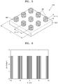
- FIG. 5 is a perspective view of an example structure of a first meta optical device 120 used in the structured light generator 100 of FIG. 4 .
- the structured light generator 120 includes a light source 110 and a first meta optical device 120 forming a distribution of light rays from light from the light source 110.
- the light source 110 may be a laser light source and may include an emission layer and a plurality of reflective layers with the emission layer therebetween.
- the first meta optical device 120 includes a first metasurface MS1 including a plurality of nanostructures NS having sub-wavelength dimensions less than a wavelength ⁇ of light emitted from the light source 110.
- a height H of a nanostructure NS is less than the wavelength ⁇ of light emitted from the light source 110.
- an arrangement distance P between the plurality of nanostructures NS is less than the wavelength ⁇ .
- the nanostructure NS is illustrated as having a cylindrical shape, but is not limited thereto.
- the nanostructure NS may have a column shape having various cross-section shapes such as a polygonal shape, a cross shape, a star shape, an asymmetric shape, etc.
- the nanostructure NS may have an asymmetric shape.
- the first meta optical device 120 may further include a substrate SU1 supporting the nanostructures NS constituting the first metasurface MS1.
- the substrate SU1 may include a dielectric material.
- a polymer material such as polycarbonate (PC), polystyrene (PS), or polymethyl methacrylate (PMMA), SiO 2 , or the like may be used to form the substrate SU1.
- the nanostructure NS may include a dielectric material, and may include a material having a refractive index greater than a refractive index of the substrate SU1.
- one of single crystal silicon, polysilicon, amorphous silicon, Si 3 N 4 , GaP, TiO 2 , AlSb, AlAs, AlGaAs, AlGalnP, BP, and ZnGeP 2 may be used to form the nanostructure NS.
- the nanostructures NS may include a conductive material.
- the conductive material may be a highly conductive metal material where surface plasmon excitation may arise.
- the nanostructures NS may include at least one selected from copper (Cu), aluminum (Al), nickel (Ni), ferrum (Fe), cobalt (Co), zinc (Zn), titanium (Ti), ruthenium (Ru), rhodium (Rh), palladium (Pd), platinum (Pt), silver (Ag), osmium (Os), iridium (Ir), and gold (Au), and may include an alloy including one of those materials.
- the nanostructures NS may include a two-dimensional material having good conductivity, such as graphene, or conductive oxide.
- some of the nanostructures NS may include a dielectric material having a high refractive index, and other nanostructures NS may include a conductive material. That is, some of the nanostructures NS may include a dielectric material having a refractive index greater than a refractive index of the substrate SU1, and other nanostructures NS may include a conductive material.
- the nanostructures NS may each have transmission intensity and transmission phases according to respective materials and shapes. Shapes of the nanostructures NS may be adjusted to adjust a phase or intensity distribution of light passing through the first metasurface MS1.
- all of the nanostructures NS illustrated have the same shape, size, and height. However, this illustration is just an example, and the exemplary embodiments are not limited thereto.
- a horizontal or vertical size or a composition material of individual nanostructures NS may be adjusted according to a location of the nanostructures NS to obtain a desired transmission intensity distribution or transmission phase distribution.
- a shape distribution of the nanostructures NS at each location may be determined with respect to a predetermined group including the nanostructures NS.
- a group of the nanostructures NS formed as such may be repeatedly arranged with a predetermined period T.
- FIG. 5 illustrates one group of the nanostructures NS, and the first metasurface MS1 may include the illustrated group of the nanostructures NS that is repeatedly arranged.
- the first metasurface MS1 may have shapes and arrangement of the nanostructures NS determined to function as a pattern generator for light emitted from the light source 110.
- the first meta optical device 120 may be configured to have a monolithic structure directly on a light exit surface 110a of the light source 110.
- a distance d between the first metasurface MS1 and the light exit surface 110a may be determined so that a contrast ratio of structured light generated by the structured light generator 100, that is, contrast, may be maximum, and a thickness of the substrate SU1 may be determined according to the determined distance d.
- Equation (1) ⁇ denotes a wavelength of light emitted from the light source 110, a 1 denotes a period at which the same structure is repeated in the first meta optical device 120, and m denotes a natural number. That is, a 1 is the period T with which the group of the nanostructures NS having the predetermined shape distribution illustrated in FIG. 5 is repeatedly arranged.
- the distance d denotes a condition where the contrast is maximum, and a distance between the first metasurface MS1 and the light exit surface 110a is not limited thereto.
- the distance d may be determined by taking into account high contrast, complexity of a structured light pattern, and the like.
- a volume of the structured light generator 100 may be greatly decreased due to the monolithically formed first meta optical device 120 being directly provided on the light exit surface 110a of the light source 110.
- the first metasurface MS1 may be very thin having a thickness of several microns or less, and accordingly, a thickness of the first meta optical device 120 may be greatly decreased to tens of microns or less.
- limitations on manufacturing for example, limitations on use in other electronic devices, may decrease, thereby enhancing price competitiveness and broadening application ranges.
- the first metasurface MS1 used in the structured light generator 100 may have shapes and an arrangement of the nanostructures NS determined to serve as a pattern generator.
- shapes and an arrangement of the nanostructures NS may be determined so that two phase modulation values with respect to incident light may be repeatedly shown.
- the first metasurface MS1 may have two phase modulation values of 0 and ⁇ .
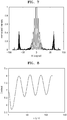
- FIG. 6 is a graph showing an example of a transmission phase change distribution caused by the first metasurface MS1 of the structured light generator 100 of FIG. 4 .
- the letter X marked on a horizontal axis of the graph denotes a one-dimensional direction in which the nanostructures NS are arranged.
- a pulse train in which the transmission phases of 0 and ⁇ repeatedly occur during a period of 0.5 um is shown, and a duty cycle of the pulse train is 0.5.
- the form of transmission phase distribution implemented is an example, and shapes, arrangement, and materials of the nanostructures NS may be variously modified to form a desired structured light pattern.
- FIG. 7 is a graph showing a distribution of light rays, that is, a structured light pattern, formed by a structured light generator having the transmission phase distribution of FIG. 6 as an intensity distribution in angular space.
- the intensity distribution is not uniform at each angular location.
- design factors of the first metasurface MS1 may be adjusted to make the intensity distribution at each angular location uniform.
- FIG. 8 is a graph showing a contrast of the structured light pattern of FIG. 7 according to a distance between the light exit surface 110a and the first metasurface MS1 in the structured light generator 100 of FIG. 4 .
- a change in contrast from a minimum value to a maximum value is repeatedly shown. It may be seen that the maximum value of the contrast repeatedly occurs when the distance d is an integer multiple of a predetermined value.
- the distance between the light exit surface 110a and the first metasurface MS1 may be determined by taking the graph of FIG. 8 into account.
- FIG. 9 shows an example of a distribution of light rays, that is, a structured light pattern, formed by the structured light generator 100 of FIG. 4 .
- Bright spots are rays of light formed over angular space by the first metasurface MS1 from incident light emitted from a light source.
- Such structured light may be used to analyze a motion of an object, a three-dimensional shape, or the like by comparing a change of pattern of the structured light that occurs when being irradiated on and reflected by the object.
- contrast indicating a difference between a bright spot and a dark portion increases, such an analysis may become easier.
- a uniform intensity distribution over angular space may make the analysis easier.
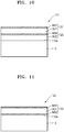
- FIG. 10 is a schematic cross-sectional view of a structure of a structured light generator 101 according to another exemplary embodiment.
- the structured light generator 101 includes the light source 110, a second meta optical device 123 on the light exit surface 110a of the light source 110, and a first meta optical device 121 on the second meta optical device 123.
- the first meta optical device 121 includes the substrate SU1 and the first metasurface MS1
- the second meta optical device 123 includes a substrate SU2 and a second metasurface MS2.
- the second metasurface MS2 is designed to serve as a beam shaper shaping light from the light source 110. That is, the second metasurface MS2 adjusts a divergence angle of light emitted from the light source 110 to be incident on the first metasurface MS1.
- the first metasurface MS1 serves as a pattern generator forming distribution of rays of light from incident light having a divergence angle and an incident beam form adjusted by the second metasurface MS2.
- the first metasurface MS1 and the second metasurface MS2 each include a plurality of nanostructures having sub wavelength dimensions, wherein shapes and arrangement of the plurality of nanostructures are designed according to each of the above functions.
- FIG. 11 is a schematic cross-sectional view of a structure of a structured light generator 102 according to another exemplary embodiment.
- the structured light generator 102 includes the light source 110, and a meta optical device 125 on the light exit surface 110a of the light source 110.
- the structured light generator 102 according to the present exemplary embodiment is modified from the structured light generator 101 of FIG. 10 in that, according to the structured light generator 102, the substrate SU1 is shared by and supports the first metasurface MS1 and the second metasurface MS2. That is, the meta optical device 125 has the first metasurface MS1 and the second metasurface MS2 respectively on both surfaces of the substrate SU1.
- the second metasurface MS2 serves as a beam shaper and directly contacts the light exit surface 110a.
- the first metasurface MS1 forms distribution of rays of light from incident light having a divergence angle and an incident beam form adjusted by the second metasurface MS2.
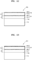
- FIG. 12 is a schematic cross-sectional view of a structure of a structured light generator 103 according to another exemplary embodiment.
- the structured light generator 103 includes the light source 110, a first meta optical device 131 and a third meta optical device 135, on the light exit surface 110a of the light source 110.
- the first meta optical device 131 includes the substrate SU1 and the first metasurface MS1, and the third meta optical device 135 includes a substrate SU3 and a third metasurface MS3.
- the first metasurface MS1 serves as a pattern generator forming distribution of rays of light from light emitted from the light source 110
- the third metasurface MS3 may be designed to serve as a duplicator duplicating the distribution of rays of light formed by the first metasurface MS1.
- the first metasurface MS1 and the third metasurface MS3 each include a plurality of nanostructures having sub wavelength dimensions, wherein shapes and an arrangement of the plurality of nanostructures are designed according to each of the above functions.
- FIG. 13 is a schematic cross-sectional view of a structure of a structured light generator 104 according to another exemplary embodiment.
- the structured light generator 104 includes the light source 110, and a meta optical device 137 on the light exit surface 110a of the light source 110.
- the structured light generator 104 according to the present exemplary embodiment is modified from the structured light generator 103 of FIG. 12 in that, according to the structured light generator 104, the substrate SU3 is shared by and supports the first metasurface MS1 and the third metasurface MS3. That is, the meta optical device 137 has the first metasurface MS1 and the third metasurface MS3 respectively on both surfaces of the substrate SU3.
- the first metasurface MS1 and the third metasurface MS3 are designed to serve as a pattern generator and a duplicator, respectively.
- the structured light generator 104 is different from the structured light generator 103 of FIG. 12 in that the first metasurface MS1 and the third metasurface MS3 are on both surfaces of one substrate SU3. Also, the substrate SU1 having a thickness which may satisfy a condition of a distance between the light exit surface 110a and the first metasurface MS1 is provided between the light source 110 and the meta optical device 137.
- Examples of a structured light generator including two metasurfaces have been described thus far. Although examples in which the two metasurfaces are designed to serve as a beam shaper and a pattern generator, respectively, or serve as a pattern generator and a duplicator, respectively, have been described, examples of the two metasurfaces are not limited thereto.
- more than two metasurfaces may be used.
- a structured light generator including three metasurfaces serving as a beam shaper, a pattern generator, and a duplicator, respectively, may be implemented.
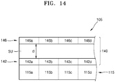
- FIG. 14 is a schematic cross-sectional view of a structure of a structured light generator 105 according to another exemplary embodiment
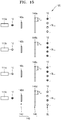
- FIG. 15 conceptually shows incident beams of a plurality of light sources being self-imaged by the structured light generator 105 of FIG. 14 to form structured light.
- the structured light generator 105 includes a light source array 115, and a meta optical device 140 on the light source array 115.
- the light source array 115 includes a plurality of light sources 115a to 115d.
- the light source array 115 may be a vertical-cavity surface-emitting laser (VCSEL) array.
- VCSEL vertical-cavity surface-emitting laser
- the meta optical device 140 includes a first metasurface array 146 and a second metasurface array 142.
- the first metasurface array 146 and the second metasurface array 142 may be respectively located on both surfaces of a substrate SU.
- a thickness d of the substrate SU may be determined to satisfy requirements for a distance between the first metasurface array 146 and the second metasurface array 142.
- the meta optical device 140 may be integrated on the light source array 115.
- the second metasurface array 142 includes a plurality of second metasurfaces 142a, 142b, 142c, and 142d respectively facing the plurality of light sources 115a, 115b, 115c, and 115d.
- the plurality of second metasurfaces 142a to 142d may serve as beam shapers shaping light emitted from the light sources 115a to 115d, respectively.
- the first metasurface array 146 includes a plurality of first metasurfaces 146a, 146b, 146c, and 146d forming distribution of rays of light from respective beams shaped by the second metasurfaces 142a to 142d.
- first metasurfaces 146a to 146d serve as pattern generators, patterns of structured lights SL a to SL d respectively generated by the first metasurfaces 146a to 146d may be different from each other. That is, the first metasurfaces 146a to 146d form image beams 12 to which an incident beam 10 emitted from each light source 115a to 115d is self-imaged, but form respectively unique patterns so that how the image beams 12 are distributed over space may be different from each other.
- the first metasurfaces 146a to 146d may each include a plurality of nanostructures having sub wavelength dimensions, but respective periods T a , T b , T c , and T d of repeatedly arranging the same structure may be different from each other.
- the structured light generator 105 is for generating complex and sophisticated structured light.
- the first metasurfaces 146a to 146d generating structured light having different patterns from each other may be disposed to correspond to the light sources 115a to 115d, respectively, so that various patterns of the structured light SL a , SL b , SL c , and SL d may be generated, and final structured light SL which is more complex and sophisticated may be formed due to overlapping of the generated patterns of the structured light SL a to SL d .
- the structured light generator 105 is not limited thereto.
- the structured light generator 105 may be modified to include a metasurface array serving as a pattern generator and a metasurface array serving as a duplicator.
- FIG. 16 is a schematic block diagram of a structure of a three-dimensional (3D) object recognition apparatus 1000 according to an exemplary embodiment.
- the 3D object recognition apparatus 1000 includes a structured light generator 1200 which radiates structured light SL i of a predetermined pattern toward an object OBJ, a sensor 1400 which receives the structured light SL r reflected from the object OBJ, and a processor 1600 which analyzes depth information, a shape, or a motion of the object OBJ having a 3D shape by comparing pattern changes in the structured light SL i radiated by the structured light generator 1200 and the structured light SL r received by the sensor 1400.
- the structured light generator 1200 may include a light source and at least one metasurface and may take the form of one of the structured light generators 100 to 105 according to the previous exemplary embodiments or a combination thereof.
- the sensor 1400 senses the structured light SL r reflected by the object OBJ.
- the processor 1600 may compare the structured light SL i radiated on the object OBJ and the structured light SL r reflected from the object OBJ with each other to analyze a 3D shape, a location, a motion, etc. of the object OBJ.
- the structured light SL i generated by the structured light generator 1200 is a pattern in which bright and dark spots are mathematically coded to uniquely designate respective angle direction location coordinates. When such a pattern is hit upon a 3D object and is reflected, a pattern of the reflected structured light SL r takes a changed form of the pattern of the radiated structured light SL i .
- 3D information of the object OBJ may be extracted by comparing those patterns with each other and tracking a pattern for each coordinate.
- the 3D object recognition apparatus 1000 may further include a controller which controls an operation of driving the light source in the structured light generator 1200, an operation of the sensor 1600, or the overall operations of the entire 3D object recognition apparatus 1000.
- the 3D object recognition apparatus 1000 may further include a memory, etc., which stores an operation program for 3D information extraction to be performed in the processor 1600.
- An operation result of the processor 1600 may be transmitted to another unit.
- the information may be transmitted to a controller of an electronic device in which the 3D object recognition apparatus 1000 is used.
- the 3D object recognition apparatus 1000 may be used as a sensor which precisely obtains 3D information regarding an object (e.g., an object in front of the 3D object recognition apparatus 1000) and thus may be used in various electronic devices.
- an electronic device may be an autonomous driving device such as a driverless car, an autonomous vehicle, a robot, or a drone, an augmented reality device, a mobile communication device, or an Internet of Things (IoT) device.
- an autonomous driving device such as a driverless car, an autonomous vehicle, a robot, or a drone
- an augmented reality device such as a mobile communication device, or an Internet of Things (IoT) device.
- IoT Internet of Things
- the structured light generator may form a distribution of rays of light (structured light) from light emitted by a light source by using a metasurface including nanostructures of a sub wavelength.
- the structured light generator according to one or more of the above exemplary embodiments uses a structure in which a meta optical device is integrated on a light source, and thus, is easy to miniaturize.
- the structured light generator may use one or more metasurfaces and adjust a distance between a light source and a metasurface, and transmission phase distribution and transmission intensity distribution of the metasurface, to generate structured light having a high contrast ratio.
- the structured light generator according to one or more of the above exemplary embodiments may be used in a 3D object recognition apparatus configured to sense a precise motion and 3D shape of an object.
Abstract
Description
- Methods and apparatuses consistent with exemplary embodiments disclosed herein relate to structured light generators for generating structured lighting and object recognition apparatuses for sensing a shape or a motion of a three-dimensional (3D) object by using the structured light generators.
- Recently, in order to recognize objects such as people or other things, accurately identifying the shape, location, motion, or the like of an object by using precise three-dimensional (3D) shape recognition has been emphasized. As one method in this regard, 3D sensing technology using structured light (a structured light system) has been developed, and thus, precise motion recognition has become possible.
- In comparison with previously used light systems, such a structured light system is required to have a smaller size and higher resolution when combined with various electronic devices. In order to generate structured light, an optical component such as a diffractive optical element (DOE) is commonly used, and the volume of such an optical component is a factor that influences the precision degree of design and manufacturing requirements.
- Exemplary embodiments disclosed herein provide structured light generators for generating structured light.
- Exemplary embodiments disclosed herein also provide three-dimensional (3D) object recognition apparatuses including structured light generators.
- Additional aspects will be set forth in part in the description which follows and, in part, will be apparent from the description, or may be learned by practice of the presented exemplary embodiments.
- According to an aspect of an exemplary embodiment, there is provided a structured light generator including a light source configured to emit light; and a first meta optical device including a first metasurface including nanostructures having sub-wavelength dimensions that are less than a wavelength of the light emitted from the light source, wherein the first metasurface is configured to form a distribution of light rays from the light emitted from the light source to thereby radiate structured light.
- The nanostructures of the first meta optical device may have forms that are configured to realize a predetermined transmission intensity distribution and transmission phase distribution with respect to the emitted light incident thereon.
- The light source may include a light exit surface through which the emitted light exits; and the first meta optical device may have a monolithic structure and may be provided directly on the light exit surface of the light source.
- The nanostructures of the first meta optical device may have shapes and an arrangement that are determined such that a transmission intensity distribution and transmission phase distribution with respect to the emitted light incident thereon are repeated.
- The nanostructures of the first meta optical device may have the shapes and distribution such that two transmission phase modulation values are obtained.
- The two transmission phase modulation values may be 0 and π.
- A distance from the light source to the first metasurface may be determined such that a contrast of a structured light pattern formed by the distribution of the light rays is a maximum.
- The distance (d) from the light source to the first metasurface may satisfy the following condition:

- The structured light generator may further include a second meta optical device provided between the light source and the first meta optical device, and the second meta optical device may include a second metasurface configured to adjust a beam shape of the light emitted from the light source.
- The first meta optical device and the second meta optical device may share a supporting substrate supporting the first metasurface and the second metasurface, and the first metasurface and the second metasurface may be respectively provided on different surfaces of the supporting substrate, the different surfaces facing each other.
- The structured light generator may further include a third meta optical device comprising a third meta surface configured to repeatedly form the distribution of the light rays formed by the first meta optical device in a predetermined angular space.
- The first meta optical device and the third meta optical device may share a substrate supporting the first metasurface and the third metasurface, and the first metasurface and the third metasurface may be respectively provided on opposite surfaces of the substrate, the opposite surfaces facing each other.
- The nanostructures may have cylindrical shapes or polygonal prismatic shapes.
- The nanostructures may have asymmetric shapes.
- The first meta optical device may further include a substrate supporting the nanostructures.
- The nanostructures may include a dielectric material having a refractive index greater than a refractive index of the substrate.
- The nanostructures may include a conductive material.
- Some nanostructures among the nanostructures may include a dielectric material having a refractive index greater than a refractive index of the substrate, and other nanostructures among the nanostructures may include a conductive material.
- According to an aspect of another exemplary embodiment, there is provided a three-dimensional (3D) object recognition apparatus including: a structured light generator including: a light source configured to emit light; and a first meta optical device including a first metasurface including nanostructures having sub-wavelength dimensions that are less than a wavelength of the light emitted from the light source, wherein the first metasurface is configured to form a distribution of light rays from the light emitted from the light source to thereby radiate structured light, and wherein the structured light generator is configured to radiate the structured light in a predetermined pattern toward an object; a sensor configured to receive the structured light reflected from the object; and a processor configured to analyze a shape or motion of the object by comparing pattern changes in the structured light radiated by the structured light generator and the structured light received by the sensor.
- According to an aspect of another exemplary embodiment, there is provided an electronic device including the 3D object recognition apparatus.
- These and/or other aspects will become apparent and more readily appreciated from the following description of the exemplary embodiments, taken in conjunction with the accompanying drawings in which:
-
FIG. 1 is a conceptual diagram of structured light formed by a metasurface used in a structured light generator according to an exemplary embodiment; -
FIG. 2 is a conceptual diagram illustrating examples of an optical function that may be performed by a metasurface used in a structured light generator according to an exemplary embodiment; -
FIG. 3 is a conceptual diagram illustrating an example of a form of a beam incident on each metasurface inFIG. 2 ; -
FIG. 4 is a schematic cross-sectional view of a structure of a structured light generator according to an exemplary embodiment; -
FIG. 5 is a perspective view of an example structure of a metasurface used in the structured light generator ofFIG. 4 ; -
FIG. 6 is a graph showing an example of a phase change distribution caused by the metasurface of the structured light generator ofFIG. 4 ; -
FIG. 7 is a graph showing distribution of rays of light, that is, a structured light pattern, formed by a structured light generator having the phase change distribution ofFIG. 6 as an intensity distribution in angular space; -
FIG. 8 is a graph showing contrast of the structured light pattern ofFIG. 7 according to a distance between a light exit surface and a metasurface in the structured light generator ofFIG. 4 ; -
FIG. 9 shows an example of distribution of rays of light, that is, a structured light pattern, formed by the structured light generator ofFIG. 4 ; -
FIG. 10 is a schematic cross-sectional view of a structure of a structured light generator according to another exemplary embodiment; -
FIG. 11 is a schematic cross-sectional view of a structure of a structured light generator according to another exemplary embodiment; -
FIG. 12 is a schematic cross-sectional view of a structure of a structured light generator according to another exemplary embodiment; -
FIG. 13 is a schematic cross-sectional view of a structure of a structured light generator according to another exemplary embodiment; -
FIG. 14 is a schematic cross-sectional view of a structure of a structured light generator according to another exemplary embodiment; -
FIG. 15 conceptually shows that incident beams from respective light sources are self-imaged in different forms by the structured light generator ofFIG. 14 to form complex structured light; and -
FIG. 16 is a schematic block diagram of a structure of a three-dimensional (3D) object recognition apparatus according to an exemplary embodiment. - Reference will now be made in detail to exemplary embodiments, examples of which are illustrated in the accompanying drawings. Like reference numerals in the drawings refer to like elements throughout, and sizes of elements in the drawings may be exaggerated for clarity and convenience of description. The present exemplary embodiments may have different forms and should not be construed as being limited to the descriptions set forth herein. Accordingly, the exemplary embodiments are merely described below, by referring to the figures, to explain aspects.
- Hereinafter, it will be understood that when an element or layer is referred to as being "formed on" another element or layer, the element or layer can be in contact with and directly formed on or in non-contact with and indirectly formed on the other element or layer.
- As used herein, the singular forms "a," "an," and "the" are intended to include the plural forms as well, unless the context clearly indicates otherwise. It will be further understood that the terms "comprises," "comprising," "includes," and/or "including," when used herein, specify the presence of other elements but do not preclude the presence or addition of other elements unless specifically stated.
- In addition, the terms such as "-or" and "-er" refer to a unit for performing at least one function or operation, and the unit may be implemented with hardware or software or a combination of hardware and software.
-
FIG. 1 is a conceptual diagram of structured light SL formed by a metasurface MS used in a structured light generator according to an exemplary embodiment. - The metasurface MS may form a distribution of light rays from light emitted from a light source LS. The light source LS may be a point light source such as a laser diode. With respect to an incident beam formed by the light source LS, the metasurface MS may form a distribution of light rays that proceed spatially. That is, light that is emitted from the light source LS and forms one
beam spot 10 is split into a plurality of light rays by the metasurface MS, and each plurality of light rays formsbeam spot images 12 over a predetermined angular space. Thebeam spot images 12 have various distributions determined by detailed conditions of the metasurface MS, and are referred to as the structured light SL. -
FIG. 2 is a conceptual diagram illustrating examples of an optical function that may be performed by a metasurface used in a structured light generator according to an exemplary embodiment, andFIG. 3 is a conceptual diagram illustrating an example of the form of a beam incident on each metasurface inFIG. 2 . - The metasurface may be realized as a beam shaper BS configured to shape a beam of incident light, a pattern generator PG configured to generate the incident light in a predetermined beam pattern, a duplicator DP configured to duplicate a pattern formed by the pattern generator PG, a combination thereof, and the like.
- The beam shaper BS may adjust a divergence angle, a beam section form, a size, or the like of light L1 emitted from the light source LS. A beam L2 shaped by the beam shaper BS is incident on the pattern generator PG and then is emitted as structured light SL' in a predetermined pattern to be incident on the duplicator DP. The duplicator DP may duplicate the structured light SL' formed by the pattern generator PG and thus may form the final structured light SL.
- In
FIGS. 2 and3 , the function that may be performed by the metasurface is illustrated in order of the beam shaper BS, the pattern generator PG, and the duplicator DP, but exemplary embodiments are not limited thereto. In order to form structured light, one or more of the beam shaper BS, the pattern generator PG, and the duplicator DP may be used, and the arrangement order may also be changed. - Various examples of a structured light generator using a metasurface will now be described.
-
FIG. 4 is a schematic cross-sectional view of a structure of a structuredlight generator 100 according to an exemplary embodiment, andFIG. 5 is a perspective view of an example structure of a first metaoptical device 120 used in the structuredlight generator 100 ofFIG. 4 . - The structured
light generator 120 includes alight source 110 and a first metaoptical device 120 forming a distribution of light rays from light from thelight source 110. - The
light source 110 may be a laser light source and may include an emission layer and a plurality of reflective layers with the emission layer therebetween. - The first meta
optical device 120 includes a first metasurface MS1 including a plurality of nanostructures NS having sub-wavelength dimensions less than a wavelength λ of light emitted from thelight source 110. A height H of a nanostructure NS is less than the wavelength λ of light emitted from thelight source 110. Also, an arrangement distance P between the plurality of nanostructures NS is less than the wavelength λ. InFIG. 5 , the nanostructure NS is illustrated as having a cylindrical shape, but is not limited thereto. In some exemplary embodiments, the nanostructure NS may have a column shape having various cross-section shapes such as a polygonal shape, a cross shape, a star shape, an asymmetric shape, etc. Alternatively, the nanostructure NS may have an asymmetric shape. - Also, the first meta
optical device 120 may further include a substrate SU1 supporting the nanostructures NS constituting the first metasurface MS1. - The substrate SU1 may include a dielectric material. For example, a polymer material, such as polycarbonate (PC), polystyrene (PS), or polymethyl methacrylate (PMMA), SiO2, or the like may be used to form the substrate SU1.
- The nanostructure NS may include a dielectric material, and may include a material having a refractive index greater than a refractive index of the substrate SU1. For example, one of single crystal silicon, polysilicon, amorphous silicon, Si3N4, GaP, TiO2, AlSb, AlAs, AlGaAs, AlGalnP, BP, and ZnGeP2 may be used to form the nanostructure NS.
- Alternatively, the nanostructures NS may include a conductive material. The conductive material may be a highly conductive metal material where surface plasmon excitation may arise. For example, the nanostructures NS may include at least one selected from copper (Cu), aluminum (Al), nickel (Ni), ferrum (Fe), cobalt (Co), zinc (Zn), titanium (Ti), ruthenium (Ru), rhodium (Rh), palladium (Pd), platinum (Pt), silver (Ag), osmium (Os), iridium (Ir), and gold (Au), and may include an alloy including one of those materials. In some exemplary embodiments, the nanostructures NS may include a two-dimensional material having good conductivity, such as graphene, or conductive oxide.
- Alternatively, some of the nanostructures NS may include a dielectric material having a high refractive index, and other nanostructures NS may include a conductive material. That is, some of the nanostructures NS may include a dielectric material having a refractive index greater than a refractive index of the substrate SU1, and other nanostructures NS may include a conductive material.
- The nanostructures NS may each have transmission intensity and transmission phases according to respective materials and shapes. Shapes of the nanostructures NS may be adjusted to adjust a phase or intensity distribution of light passing through the first metasurface MS1. In
FIG. 5 , all of the nanostructures NS illustrated have the same shape, size, and height. However, this illustration is just an example, and the exemplary embodiments are not limited thereto. For example, a horizontal or vertical size or a composition material of individual nanostructures NS may be adjusted according to a location of the nanostructures NS to obtain a desired transmission intensity distribution or transmission phase distribution. In order to obtain the desired transmission intensity distribution or transmission phase distribution, a shape distribution of the nanostructures NS at each location may be determined with respect to a predetermined group including the nanostructures NS. Also, a group of the nanostructures NS formed as such may be repeatedly arranged with a predetermined period T. For example,FIG. 5 illustrates one group of the nanostructures NS, and the first metasurface MS1 may include the illustrated group of the nanostructures NS that is repeatedly arranged. - The first metasurface MS1 may have shapes and arrangement of the nanostructures NS determined to function as a pattern generator for light emitted from the
light source 110. - The first meta
optical device 120 may be configured to have a monolithic structure directly on alight exit surface 110a of thelight source 110. When the first metasurface MS1 includes a group of the nanostructures NS repeatedly arranged with the predetermined period T, a distance d between the first metasurface MS1 and thelight exit surface 110a may be determined so that a contrast ratio of structured light generated by the structuredlight generator 100, that is, contrast, may be maximum, and a thickness of the substrate SU1 may be determined according to the determined distance d. The distance d may be calculated using the following equation (1):
- In Equation (1), λ denotes a wavelength of light emitted from the
light source 110, a1 denotes a period at which the same structure is repeated in the first metaoptical device 120, and m denotes a natural number. That is, a1 is the period T with which the group of the nanostructures NS having the predetermined shape distribution illustrated inFIG. 5 is repeatedly arranged. - The distance d denotes a condition where the contrast is maximum, and a distance between the first metasurface MS1 and the
light exit surface 110a is not limited thereto. For example, the distance d may be determined by taking into account high contrast, complexity of a structured light pattern, and the like. - A volume of the structured
light generator 100 may be greatly decreased due to the monolithically formed first metaoptical device 120 being directly provided on thelight exit surface 110a of thelight source 110. The first metasurface MS1 may be very thin having a thickness of several microns or less, and accordingly, a thickness of the first metaoptical device 120 may be greatly decreased to tens of microns or less. As the whole volume of the structuredlight generator 100 greatly decreases, limitations on manufacturing, for example, limitations on use in other electronic devices, may decrease, thereby enhancing price competitiveness and broadening application ranges. - The first metasurface MS1 used in the structured
light generator 100 according to the present exemplary embodiment may have shapes and an arrangement of the nanostructures NS determined to serve as a pattern generator. For example, shapes and an arrangement of the nanostructures NS may be determined so that two phase modulation values with respect to incident light may be repeatedly shown. For example, the first metasurface MS1 may have two phase modulation values of 0 and π. -
FIG. 6 is a graph showing an example of a transmission phase change distribution caused by the first metasurface MS1 of the structuredlight generator 100 ofFIG. 4 . - The letter X marked on a horizontal axis of the graph denotes a one-dimensional direction in which the nanostructures NS are arranged. Referring to the graph, a pulse train in which the transmission phases of 0 and π repeatedly occur during a period of 0.5 um is shown, and a duty cycle of the pulse train is 0.5. The form of transmission phase distribution implemented is an example, and shapes, arrangement, and materials of the nanostructures NS may be variously modified to form a desired structured light pattern.
-
FIG. 7 is a graph showing a distribution of light rays, that is, a structured light pattern, formed by a structured light generator having the transmission phase distribution ofFIG. 6 as an intensity distribution in angular space. - Referring to
FIG. 7 , the intensity distribution is not uniform at each angular location. However, design factors of the first metasurface MS1 may be adjusted to make the intensity distribution at each angular location uniform. -
FIG. 8 is a graph showing a contrast of the structured light pattern ofFIG. 7 according to a distance between thelight exit surface 110a and the first metasurface MS1 in the structuredlight generator 100 ofFIG. 4 . - Referring to
FIG. 8 , a change in contrast from a minimum value to a maximum value is repeatedly shown. It may be seen that the maximum value of the contrast repeatedly occurs when the distance d is an integer multiple of a predetermined value. The distance between thelight exit surface 110a and the first metasurface MS1 may be determined by taking the graph ofFIG. 8 into account. -
FIG. 9 shows an example of a distribution of light rays, that is, a structured light pattern, formed by the structuredlight generator 100 ofFIG. 4 . - Bright spots are rays of light formed over angular space by the first metasurface MS1 from incident light emitted from a light source. Such structured light may be used to analyze a motion of an object, a three-dimensional shape, or the like by comparing a change of pattern of the structured light that occurs when being irradiated on and reflected by the object. In this respect, as contrast indicating a difference between a bright spot and a dark portion increases, such an analysis may become easier. Also, a uniform intensity distribution over angular space may make the analysis easier.
-
FIG. 10 is a schematic cross-sectional view of a structure of a structuredlight generator 101 according to another exemplary embodiment. - The structured
light generator 101 includes thelight source 110, a second metaoptical device 123 on thelight exit surface 110a of thelight source 110, and a first metaoptical device 121 on the second metaoptical device 123. - The first meta
optical device 121 includes the substrate SU1 and the first metasurface MS1, and the second metaoptical device 123 includes a substrate SU2 and a second metasurface MS2. - In the present exemplary embodiment, the second metasurface MS2 is designed to serve as a beam shaper shaping light from the
light source 110. That is, the second metasurface MS2 adjusts a divergence angle of light emitted from thelight source 110 to be incident on the first metasurface MS1. The first metasurface MS1 serves as a pattern generator forming distribution of rays of light from incident light having a divergence angle and an incident beam form adjusted by the second metasurface MS2. - The first metasurface MS1 and the second metasurface MS2 each include a plurality of nanostructures having sub wavelength dimensions, wherein shapes and arrangement of the plurality of nanostructures are designed according to each of the above functions.
-
FIG. 11 is a schematic cross-sectional view of a structure of a structuredlight generator 102 according to another exemplary embodiment. - The structured
light generator 102 includes thelight source 110, and a meta optical device 125 on thelight exit surface 110a of thelight source 110. The structuredlight generator 102 according to the present exemplary embodiment is modified from the structuredlight generator 101 ofFIG. 10 in that, according to the structuredlight generator 102, the substrate SU1 is shared by and supports the first metasurface MS1 and the second metasurface MS2. That is, the meta optical device 125 has the first metasurface MS1 and the second metasurface MS2 respectively on both surfaces of the substrate SU1. The second metasurface MS2 serves as a beam shaper and directly contacts thelight exit surface 110a. The first metasurface MS1 forms distribution of rays of light from incident light having a divergence angle and an incident beam form adjusted by the second metasurface MS2. -
FIG. 12 is a schematic cross-sectional view of a structure of a structuredlight generator 103 according to another exemplary embodiment. - The structured
light generator 103 includes thelight source 110, a first metaoptical device 131 and a third metaoptical device 135, on thelight exit surface 110a of thelight source 110. - The first meta
optical device 131 includes the substrate SU1 and the first metasurface MS1, and the third metaoptical device 135 includes a substrate SU3 and a third metasurface MS3. - In the present exemplary embodiment, the first metasurface MS1 serves as a pattern generator forming distribution of rays of light from light emitted from the
light source 110, and the third metasurface MS3 may be designed to serve as a duplicator duplicating the distribution of rays of light formed by the first metasurface MS1. - The first metasurface MS1 and the third metasurface MS3 each include a plurality of nanostructures having sub wavelength dimensions, wherein shapes and an arrangement of the plurality of nanostructures are designed according to each of the above functions.
-
FIG. 13 is a schematic cross-sectional view of a structure of a structuredlight generator 104 according to another exemplary embodiment. - The structured
light generator 104 includes thelight source 110, and a metaoptical device 137 on thelight exit surface 110a of thelight source 110. The structuredlight generator 104 according to the present exemplary embodiment is modified from the structuredlight generator 103 ofFIG. 12 in that, according to the structuredlight generator 104, the substrate SU3 is shared by and supports the first metasurface MS1 and the third metasurface MS3. That is, the metaoptical device 137 has the first metasurface MS1 and the third metasurface MS3 respectively on both surfaces of the substrate SU3. The first metasurface MS1 and the third metasurface MS3 are designed to serve as a pattern generator and a duplicator, respectively. - The structured
light generator 104 according to the present exemplary embodiment is different from the structuredlight generator 103 ofFIG. 12 in that the first metasurface MS1 and the third metasurface MS3 are on both surfaces of one substrate SU3. Also, the substrate SU1 having a thickness which may satisfy a condition of a distance between thelight exit surface 110a and the first metasurface MS1 is provided between thelight source 110 and the metaoptical device 137. - Examples of a structured light generator including two metasurfaces have been described thus far. Although examples in which the two metasurfaces are designed to serve as a beam shaper and a pattern generator, respectively, or serve as a pattern generator and a duplicator, respectively, have been described, examples of the two metasurfaces are not limited thereto.
- In addition, according to certain exemplary embodiments, more than two metasurfaces may be used. For example, a structured light generator including three metasurfaces serving as a beam shaper, a pattern generator, and a duplicator, respectively, may be implemented.
-
FIG. 14 is a schematic cross-sectional view of a structure of a structuredlight generator 105 according to another exemplary embodiment, andFIG. 15 conceptually shows incident beams of a plurality of light sources being self-imaged by the structuredlight generator 105 ofFIG. 14 to form structured light. - The structured
light generator 105 includes alight source array 115, and a metaoptical device 140 on thelight source array 115. - The
light source array 115 includes a plurality oflight sources 115a to 115d. For example, thelight source array 115 may be a vertical-cavity surface-emitting laser (VCSEL) array. - The meta
optical device 140 includes afirst metasurface array 146 and asecond metasurface array 142. Thefirst metasurface array 146 and thesecond metasurface array 142 may be respectively located on both surfaces of a substrate SU. A thickness d of the substrate SU may be determined to satisfy requirements for a distance between thefirst metasurface array 146 and thesecond metasurface array 142. - The meta
optical device 140 may be integrated on thelight source array 115. - The
second metasurface array 142 includes a plurality of second metasurfaces 142a, 142b, 142c, and 142d respectively facing the plurality oflight sources light sources 115a to 115d, respectively. - The
first metasurface array 146 includes a plurality of first metasurfaces 146a, 146b, 146c, and 146d forming distribution of rays of light from respective beams shaped by the second metasurfaces 142a to 142d. - Although all of the plurality of first metasurfaces 146a to 146d serve as pattern generators, patterns of structured lights SLa to SLd respectively generated by the first metasurfaces 146a to 146d may be different from each other. That is, the first metasurfaces 146a to 146d form image beams 12 to which an
incident beam 10 emitted from eachlight source 115a to 115d is self-imaged, but form respectively unique patterns so that how the image beams 12 are distributed over space may be different from each other. To achieve this feature, the first metasurfaces 146a to 146d may each include a plurality of nanostructures having sub wavelength dimensions, but respective periods Ta, Tb, Tc, and Td of repeatedly arranging the same structure may be different from each other. - The structured
light generator 105 is for generating complex and sophisticated structured light. The first metasurfaces 146a to 146d generating structured light having different patterns from each other may be disposed to correspond to thelight sources 115a to 115d, respectively, so that various patterns of the structured light SLa, SLb, SLc, and SLd may be generated, and final structured light SL which is more complex and sophisticated may be formed due to overlapping of the generated patterns of the structured light SLa to SLd. - Although an example of the structured
light generator 105 in which thesecond metasurface array 142 serving as a beam shaper and thefirst metasurface array 146 serving as a pattern generator are provided on thelight source array 115 is shown, the structuredlight generator 105 is not limited thereto. The structuredlight generator 105 may be modified to include a metasurface array serving as a pattern generator and a metasurface array serving as a duplicator. -
FIG. 16 is a schematic block diagram of a structure of a three-dimensional (3D) objectrecognition apparatus 1000 according to an exemplary embodiment. - The 3D
object recognition apparatus 1000 includes a structuredlight generator 1200 which radiates structured light SLi of a predetermined pattern toward an object OBJ, asensor 1400 which receives the structured light SLr reflected from the object OBJ, and aprocessor 1600 which analyzes depth information, a shape, or a motion of the object OBJ having a 3D shape by comparing pattern changes in the structured light SLi radiated by the structuredlight generator 1200 and the structured light SLr received by thesensor 1400. - The structured
light generator 1200 may include a light source and at least one metasurface and may take the form of one of the structuredlight generators 100 to 105 according to the previous exemplary embodiments or a combination thereof. - The
sensor 1400 senses the structured light SLr reflected by the object OBJ. - The
processor 1600 may compare the structured light SLi radiated on the object OBJ and the structured light SLr reflected from the object OBJ with each other to analyze a 3D shape, a location, a motion, etc. of the object OBJ. The structured light SLi generated by the structuredlight generator 1200 is a pattern in which bright and dark spots are mathematically coded to uniquely designate respective angle direction location coordinates. When such a pattern is hit upon a 3D object and is reflected, a pattern of the reflected structured light SLr takes a changed form of the pattern of the radiated structured light SLi. 3D information of the object OBJ may be extracted by comparing those patterns with each other and tracking a pattern for each coordinate. - The 3D
object recognition apparatus 1000 may further include a controller which controls an operation of driving the light source in the structuredlight generator 1200, an operation of thesensor 1600, or the overall operations of the entire 3Dobject recognition apparatus 1000. In addition, the 3Dobject recognition apparatus 1000 may further include a memory, etc., which stores an operation program for 3D information extraction to be performed in theprocessor 1600. - An operation result of the
processor 1600, that is, information regarding a shape and a location of the object OBJ, may be transmitted to another unit. For example, the information may be transmitted to a controller of an electronic device in which the 3Dobject recognition apparatus 1000 is used. - The 3D
object recognition apparatus 1000 may be used as a sensor which precisely obtains 3D information regarding an object (e.g., an object in front of the 3D object recognition apparatus 1000) and thus may be used in various electronic devices. For example, such an electronic device may be an autonomous driving device such as a driverless car, an autonomous vehicle, a robot, or a drone, an augmented reality device, a mobile communication device, or an Internet of Things (IoT) device. - The structured light generator according to one or more of the above exemplary embodiments may form a distribution of rays of light (structured light) from light emitted by a light source by using a metasurface including nanostructures of a sub wavelength.
- The structured light generator according to one or more of the above exemplary embodiments uses a structure in which a meta optical device is integrated on a light source, and thus, is easy to miniaturize.
- The structured light generator according to one or more of the above exemplary embodiments may use one or more metasurfaces and adjust a distance between a light source and a metasurface, and transmission phase distribution and transmission intensity distribution of the metasurface, to generate structured light having a high contrast ratio.
- The structured light generator according to one or more of the above exemplary embodiments may be used in a 3D object recognition apparatus configured to sense a precise motion and 3D shape of an object.
- It should be understood that the exemplary embodiments described herein should be considered in a descriptive sense only and not for purposes of limitation. Descriptions of features or aspects within each exemplary embodiment should typically be considered as available for other similar features or aspects in other exemplary embodiments.
- While one or more exemplary embodiments have been described with reference to the figures, it will be understood by those of ordinary skill in the art that various changes in form and details may be made therein without departing from the scope as defined by the following claims.
Claims (15)
- A structured light generator comprising:a light source configured to emit light; anda first meta optical device comprising a first metasurface comprising nanostructures having sub-wavelength dimensions that are less than a wavelength of the light emitted from the light source,wherein the first metasurface is configured to form a distribution of light rays from the light emitted from the light source to thereby radiate structured light.
- The structured light generator of claim 1, wherein the nanostructures of the first meta optical device have forms that are configured to realize a predetermined transmission intensity distribution and transmission phase distribution with respect to the emitted light incident thereon.
- The structured light generator of claim 1 or 2, wherein:the light source comprises a light exit surface through which the emitted light exits; andthe first meta optical device has a monolithic structure and is provided directly on the light exit surface of the light source.
- The structured light generator of any preceding claim, wherein the nanostructures of the first meta optical device have shapes and an arrangement that are determined such that a transmission intensity distribution and transmission phase distribution with respect to the emitted light incident thereon are repeated.
- The structured light generator of claim 4, wherein the nanostructures of the first meta optical device have the shapes and distribution such that two transmission phase modulation values are obtained, and preferably wherein the two transmission phase modulation values are 0 and π.
- The structured light generator of claim 4 or 5, wherein a distance from the light source to the first metasurface is determined such that a contrast of a structured light pattern formed by the distribution of the light rays is a maximum, and preferably wherein the distance (d) from the light source to the first metasurface satisfies the following condition:

- The structured light generator of any preceding claim, further comprising a second meta optical device provided between the light source and the first meta optical device, the second meta optical device comprising a second metasurface configured to adjust a beam shape of the light emitted from the light source, and preferably wherein: the first meta optical device and the second meta optical device share a supporting substrate supporting the first metasurface and the second metasurface; and
the first metasurface and the second metasurface are respectively provided on different surfaces of the supporting substrate, the different surfaces facing each other. - The structured light generator of any preceding claim, further comprising a third meta optical device comprising a third meta surface configured to repeatedly form the distribution of the light rays formed by the first meta optical device in a predetermined angular space, and preferably wherein the first meta optical device and the third meta optical device share a substrate supporting the first metasurface and the third metasurface, and
the first metasurface and the third metasurface are respectively provided on opposite surfaces of the substrate, the opposite surfaces facing each other. - The structured light generator of any preceding claim, wherein the nanostructures have cylindrical shapes or polygonal prismatic shapes.
- The structured light generator of any preceding claim, wherein the nanostructures have asymmetric shapes.
- The structured light generator of any preceding claim, wherein the first meta optical device further comprises a substrate supporting the nanostructures.
- The structured light generator of claim 11, wherein the nanostructures comprise either: a dielectric material having a refractive index greater than a refractive index of the substrate; or a conductive material.
- The structured light generator of claim 11 or 12, wherein some nanostructures among the nanostructures comprise a dielectric material having a refractive index greater than a refractive index of the substrate, and other nanostructures among the nanostructures comprise a conductive material.
- A three-dimensional, 3D, object recognition apparatus comprising:a structured light generator according to any preceding claim, wherein the structured light generator is configured to radiate the structured light in a predetermined pattern toward an object;a sensor configured to receive the structured light reflected from the object; anda processor configured to analyze a shape or motion of the object by comparing pattern changes in the structured light radiated by the structured light generator and the structured light received by the sensor.
- An electronic device comprising the 3D object recognition apparatus of claim 14.
Applications Claiming Priority (2)
| Application Number | Priority Date | Filing Date | Title |
|---|---|---|---|
| US201662315267P | 2016-03-30 | 2016-03-30 | |
| KR1020160112087A KR102629586B1 (en) | 2016-03-30 | 2016-08-31 | Structured light generator and apparatus for recognizing 3-dimensional object including the same |
Publications (2)
| Publication Number | Publication Date |
|---|---|
| EP3226042A1 true EP3226042A1 (en) | 2017-10-04 |
| EP3226042B1 EP3226042B1 (en) | 2022-05-04 |
Family
ID=80857392
Family Applications (1)
| Application Number | Title | Priority Date | Filing Date |
|---|---|---|---|
| EP17152279.0A Active EP3226042B1 (en) | 2016-03-30 | 2017-01-19 | Structured light generator and object recognition apparatus including the same |
Country Status (1)
| Country | Link |
|---|---|
| EP (1) | EP3226042B1 (en) |
Cited By (17)
| Publication number | Priority date | Publication date | Assignee | Title |
|---|---|---|---|---|
| EP3550334A1 (en) * | 2018-04-04 | 2019-10-09 | Samsung Electronics Co., Ltd. | Light source module including transparent member with meta-surface and electronic device comprising the same |
| EP3650808A1 (en) * | 2018-11-09 | 2020-05-13 | Samsung Electronics Co., Ltd. | Structured light projector and electronic device including the same |
| WO2020165448A1 (en) * | 2019-02-15 | 2020-08-20 | Université D'aix-Marseille | Optical metasurfaces, and associated manufacturing methods and systems |
| US10795168B2 (en) | 2017-08-31 | 2020-10-06 | Metalenz, Inc. | Transmissive metasurface lens integration |
| WO2020229576A3 (en) * | 2019-05-14 | 2021-01-07 | Osram Opto Semiconductors Gmbh | Illumination unit, method for producing an illumination unit, converter element for an optoelectronic component, radiation source including an led and a converter element, outcoupling structure, and optoelectronic device |
| US11156759B2 (en) | 2019-01-29 | 2021-10-26 | Osram Opto Semiconductors Gmbh | μ-LED, μ-LED device, display and method for the same |
| EP3721295A4 (en) * | 2017-12-04 | 2022-01-05 | California Institute of Technology | Metasurface-assisted 3d beam shaping |
| US11271143B2 (en) | 2019-01-29 | 2022-03-08 | Osram Opto Semiconductors Gmbh | μ-LED, μ-LED device, display and method for the same |
| US11302248B2 (en) | 2019-01-29 | 2022-04-12 | Osram Opto Semiconductors Gmbh | U-led, u-led device, display and method for the same |
| CN114877825A (en) * | 2022-05-16 | 2022-08-09 | 浙江大学 | Linear spectrum confocal system for three-dimensional surface type measurement based on super-surface light splitting |
| US11538852B2 (en) | 2019-04-23 | 2022-12-27 | Osram Opto Semiconductors Gmbh | μ-LED, μ-LED device, display and method for the same |
| US11610868B2 (en) | 2019-01-29 | 2023-03-21 | Osram Opto Semiconductors Gmbh | μ-LED, μ-LED device, display and method for the same |
| CN116222433A (en) * | 2023-03-22 | 2023-06-06 | 西安知象光电科技有限公司 | Structured light three-dimensional imaging system and method based on super surface |
| WO2023208817A1 (en) * | 2022-04-26 | 2023-11-02 | Ams International Ag | Illumination apparatus |
| US11906698B2 (en) | 2017-05-24 | 2024-02-20 | The Trustees Of Columbia University In The City Of New York | Broadband achromatic flat optical components by dispersion-engineered dielectric metasurfaces |
| US11927769B2 (en) | 2022-03-31 | 2024-03-12 | Metalenz, Inc. | Polarization sorting metasurface microlens array device |
| US11978752B2 (en) | 2019-07-26 | 2024-05-07 | Metalenz, Inc. | Aperture-metasurface and hybrid refractive-metasurface imaging systems |
Citations (4)
| Publication number | Priority date | Publication date | Assignee | Title |
|---|---|---|---|---|
| US20110180779A1 (en) * | 2010-01-22 | 2011-07-28 | Samsung Electronics Co., Ltd. | Nanostructured thin film, surface light source and display apparatus employing nanostructured thin film |
| FR3007148A1 (en) * | 2013-06-17 | 2014-12-19 | Centre Nat Rech Scient | ANGULAR OPTICAL FILTERING ELEMENT FOR ANGULAR FILTERING WITH CONTROLLED ANGULAR SELECTIVITY |
| EP2831538A1 (en) * | 2012-03-26 | 2015-02-04 | Mantisvision Ltd. | Three dimensional camera and projector for same |
| WO2015054601A2 (en) * | 2013-10-11 | 2015-04-16 | Duke University | Multi-sensor compressive imaging |
-
2017
- 2017-01-19 EP EP17152279.0A patent/EP3226042B1/en active Active
Patent Citations (4)
| Publication number | Priority date | Publication date | Assignee | Title |
|---|---|---|---|---|
| US20110180779A1 (en) * | 2010-01-22 | 2011-07-28 | Samsung Electronics Co., Ltd. | Nanostructured thin film, surface light source and display apparatus employing nanostructured thin film |
| EP2831538A1 (en) * | 2012-03-26 | 2015-02-04 | Mantisvision Ltd. | Three dimensional camera and projector for same |
| FR3007148A1 (en) * | 2013-06-17 | 2014-12-19 | Centre Nat Rech Scient | ANGULAR OPTICAL FILTERING ELEMENT FOR ANGULAR FILTERING WITH CONTROLLED ANGULAR SELECTIVITY |
| WO2015054601A2 (en) * | 2013-10-11 | 2015-04-16 | Duke University | Multi-sensor compressive imaging |
Non-Patent Citations (2)
| Title |
|---|
| ANONYMOUS: "Electromagnetic metasurface - Wikipedia", WIKIPEDIA, 12 March 2017 (2017-03-12), XP055395329, Retrieved from the Internet <URL:https://en.wikipedia.org/wiki/Electromagnetic_metasurface> [retrieved on 20170802] * |
| JINWEI ZENG ET AL: "Manipulating Complex Light with Metamaterials", SCIENTIFIC REPORTS, vol. 3, no. 1, 2 October 2013 (2013-10-02), XP055394391, DOI: 10.1038/srep02826 * |
Cited By (31)
| Publication number | Priority date | Publication date | Assignee | Title |
|---|---|---|---|---|
| US11906698B2 (en) | 2017-05-24 | 2024-02-20 | The Trustees Of Columbia University In The City Of New York | Broadband achromatic flat optical components by dispersion-engineered dielectric metasurfaces |
| US11579456B2 (en) | 2017-08-31 | 2023-02-14 | Metalenz, Inc. | Transmissive metasurface lens integration |
| US10795168B2 (en) | 2017-08-31 | 2020-10-06 | Metalenz, Inc. | Transmissive metasurface lens integration |
| US11450970B2 (en) | 2017-12-04 | 2022-09-20 | California Institute Of Technology | Metasurface-assisted 3D beam shaping for desired phase, amplitude, and polarization |
| EP3721295A4 (en) * | 2017-12-04 | 2022-01-05 | California Institute of Technology | Metasurface-assisted 3d beam shaping |
| EP3550334A1 (en) * | 2018-04-04 | 2019-10-09 | Samsung Electronics Co., Ltd. | Light source module including transparent member with meta-surface and electronic device comprising the same |
| US10920957B2 (en) | 2018-04-04 | 2021-02-16 | Samsung Electronics Co., Ltd. | Light source module including transparent member with meta-surface and electronic device comprising the same |
| US11067877B2 (en) | 2018-11-09 | 2021-07-20 | Samsung Electronics Co., Ltd. | Structured light projector and electronic device including the same |
| US11880123B2 (en) | 2018-11-09 | 2024-01-23 | Samsung Electronics Co., Ltd. | Structured light projector and electronic device including the same |
| EP3650808A1 (en) * | 2018-11-09 | 2020-05-13 | Samsung Electronics Co., Ltd. | Structured light projector and electronic device including the same |
| US11592733B2 (en) | 2018-11-09 | 2023-02-28 | Samsung Electronics Co., Ltd. | Structured light projector and electronic device including the same |
| US11513275B2 (en) | 2019-01-29 | 2022-11-29 | Osram Opto Semiconductors Gmbh | μ-LED, μ-LED device, display and method for the same |
| US11302248B2 (en) | 2019-01-29 | 2022-04-12 | Osram Opto Semiconductors Gmbh | U-led, u-led device, display and method for the same |
| US11156759B2 (en) | 2019-01-29 | 2021-10-26 | Osram Opto Semiconductors Gmbh | μ-LED, μ-LED device, display and method for the same |
| US11764339B2 (en) | 2019-01-29 | 2023-09-19 | Osram Opto Semiconductors Gmbh | μ-LED, μ-LED device, display and method for the same |
| US11480723B2 (en) | 2019-01-29 | 2022-10-25 | Osram Opto Semiconductors Gmbh | μ-LED, μ-LED device, display and method for the same |
| US11271143B2 (en) | 2019-01-29 | 2022-03-08 | Osram Opto Semiconductors Gmbh | μ-LED, μ-LED device, display and method for the same |
| US11610868B2 (en) | 2019-01-29 | 2023-03-21 | Osram Opto Semiconductors Gmbh | μ-LED, μ-LED device, display and method for the same |
| WO2020165448A1 (en) * | 2019-02-15 | 2020-08-20 | Université D'aix-Marseille | Optical metasurfaces, and associated manufacturing methods and systems |
| EP3924757B1 (en) * | 2019-02-15 | 2023-03-22 | Université d'Aix-Marseille | Optical metasurfaces, and associated manufacturing methods and systems |
| CN113728249A (en) * | 2019-02-15 | 2021-11-30 | 艾克斯-马赛大学 | Optical super-surface and related manufacturing method and system |
| FR3092915A1 (en) * | 2019-02-15 | 2020-08-21 | Université D'aix-Marseille | Optical metasurfaces, associated manufacturing processes and systems |
| US11538852B2 (en) | 2019-04-23 | 2022-12-27 | Osram Opto Semiconductors Gmbh | μ-LED, μ-LED device, display and method for the same |
| WO2020229576A3 (en) * | 2019-05-14 | 2021-01-07 | Osram Opto Semiconductors Gmbh | Illumination unit, method for producing an illumination unit, converter element for an optoelectronic component, radiation source including an led and a converter element, outcoupling structure, and optoelectronic device |
| US11978752B2 (en) | 2019-07-26 | 2024-05-07 | Metalenz, Inc. | Aperture-metasurface and hybrid refractive-metasurface imaging systems |
| US11927769B2 (en) | 2022-03-31 | 2024-03-12 | Metalenz, Inc. | Polarization sorting metasurface microlens array device |
| WO2023208817A1 (en) * | 2022-04-26 | 2023-11-02 | Ams International Ag | Illumination apparatus |
| CN114877825A (en) * | 2022-05-16 | 2022-08-09 | 浙江大学 | Linear spectrum confocal system for three-dimensional surface type measurement based on super-surface light splitting |
| CN114877825B (en) * | 2022-05-16 | 2023-08-01 | 浙江大学 | Linear spectrum confocal system for three-dimensional surface type measurement based on super-surface light splitting |
| CN116222433B (en) * | 2023-03-22 | 2023-09-05 | 西安知象光电科技有限公司 | Structured light three-dimensional imaging system and method based on super surface |
| CN116222433A (en) * | 2023-03-22 | 2023-06-06 | 西安知象光电科技有限公司 | Structured light three-dimensional imaging system and method based on super surface |
Also Published As
| Publication number | Publication date |
|---|---|
| EP3226042B1 (en) | 2022-05-04 |
Similar Documents
| Publication | Publication Date | Title |
|---|---|---|
| US11035548B2 (en) | Structured light generator and object recognition apparatus including the same | |
| EP3226042A1 (en) | Structured light generator and object recognition apparatus including the same | |
| KR102629586B1 (en) | Structured light generator and apparatus for recognizing 3-dimensional object including the same | |
| JP7269712B2 (en) | Projector with metalens | |
| TWI716533B (en) | Multi-mode illumination module and related method | |
| US11441755B2 (en) | Illumination device and electronic apparatus including the same | |
| CN110221447B (en) | Structured light projection diffraction optical device based on super-structured surface | |
| CN111399245A (en) | Laser emission module and 3D imaging device | |
| EP3274653B1 (en) | Depth mapping with a head mounted display using stereo cameras and structured light | |
| EP2885672B1 (en) | Illumination light shaping for a depth camera | |
| US8836761B2 (en) | 3D information generator for use in interactive interface and method for 3D information generation | |
| JP2020527724A (en) | VCSEL array LIDAR transmitter with small angle divergence | |
| EP2466905B1 (en) | Illumination optical system and 3D image acquisition apparatus including the same | |
| RU2661743C2 (en) | Pixel mapping and printing for micro lens arrays to achieve dual-axis activation of images | |
| EP3637566B1 (en) | Back side emitting light source array device and electronic apparatus having the same | |
| CN112534306B (en) | Structured light projector including integrated superlens and diffractive optical element | |
| KR102129244B1 (en) | Using depth in three-dimensional object printing to form colors that change with viewing and illumination angles | |
| EP3644110A1 (en) | Optical element and optical system | |
| CN112514179A (en) | Laser arrangement with reduced build height | |
| CN102189879A (en) | Manufacturing method for a shaped article having a very fine uneven surface structure | |
| CN211878344U (en) | Laser emission module and 3D imaging device | |
| CN112433382A (en) | Speckle projection device and method, electronic device and distance measurement system | |
| CN101578611A (en) | Device and method for recording information in a data carrier | |
| US20210325686A1 (en) | Diffractive optical element with collimator function | |
| TWI785400B (en) | Light source, sensor and method of illuminating a scene |
Legal Events
| Date | Code | Title | Description |
|---|---|---|---|
| PUAI | Public reference made under article 153(3) epc to a published international application that has entered the european phase |
Free format text: ORIGINAL CODE: 0009012 |
|
| STAA | Information on the status of an ep patent application or granted ep patent |
Free format text: STATUS: THE APPLICATION HAS BEEN PUBLISHED |
|
| AK | Designated contracting states |
Kind code of ref document: A1 Designated state(s): AL AT BE BG CH CY CZ DE DK EE ES FI FR GB GR HR HU IE IS IT LI LT LU LV MC MK MT NL NO PL PT RO RS SE SI SK SM TR |
|
| AX | Request for extension of the european patent |
Extension state: BA ME |
|
| STAA | Information on the status of an ep patent application or granted ep patent |
Free format text: STATUS: REQUEST FOR EXAMINATION WAS MADE |
|
| 17P | Request for examination filed |
Effective date: 20180404 |
|
| RBV | Designated contracting states (corrected) |
Designated state(s): AL AT BE BG CH CY CZ DE DK EE ES FI FR GB GR HR HU IE IS IT LI LT LU LV MC MK MT NL NO PL PT RO RS SE SI SK SM TR |
|
| STAA | Information on the status of an ep patent application or granted ep patent |
Free format text: STATUS: EXAMINATION IS IN PROGRESS |
|
| 17Q | First examination report despatched |
Effective date: 20190920 |
|
| STAA | Information on the status of an ep patent application or granted ep patent |
Free format text: STATUS: EXAMINATION IS IN PROGRESS |
|
| GRAP | Despatch of communication of intention to grant a patent |
Free format text: ORIGINAL CODE: EPIDOSNIGR1 |
|
| STAA | Information on the status of an ep patent application or granted ep patent |
Free format text: STATUS: GRANT OF PATENT IS INTENDED |
|
| INTG | Intention to grant announced |
Effective date: 20211206 |
|
| RIN1 | Information on inventor provided before grant (corrected) |
Inventor name: ATWATER, HARRY Inventor name: NAQAVI, ALI Inventor name: HAN, SEUNGHOON |
|
| GRAS | Grant fee paid |
Free format text: ORIGINAL CODE: EPIDOSNIGR3 |
|
| GRAA | (expected) grant |
Free format text: ORIGINAL CODE: 0009210 |
|
| STAA | Information on the status of an ep patent application or granted ep patent |
Free format text: STATUS: THE PATENT HAS BEEN GRANTED |
|
| AK | Designated contracting states |
Kind code of ref document: B1 Designated state(s): AL AT BE BG CH CY CZ DE DK EE ES FI FR GB GR HR HU IE IS IT LI LT LU LV MC MK MT NL NO PL PT RO RS SE SI SK SM TR |
|
| REG | Reference to a national code |
Ref country code: GB Ref legal event code: FG4D |
|
| REG | Reference to a national code |
Ref country code: CH Ref legal event code: EP |
|
| REG | Reference to a national code |
Ref country code: AT Ref legal event code: REF Ref document number: 1489653 Country of ref document: AT Kind code of ref document: T Effective date: 20220515 |
|
| REG | Reference to a national code |
Ref country code: IE Ref legal event code: FG4D Ref country code: DE Ref legal event code: R096 Ref document number: 602017056774 Country of ref document: DE |
|
| REG | Reference to a national code |
Ref country code: LT Ref legal event code: MG9D |
|
| REG | Reference to a national code |
Ref country code: NL Ref legal event code: MP Effective date: 20220504 |
|
| REG | Reference to a national code |
Ref country code: AT Ref legal event code: MK05 Ref document number: 1489653 Country of ref document: AT Kind code of ref document: T Effective date: 20220504 |
|
| PG25 | Lapsed in a contracting state [announced via postgrant information from national office to epo] |
Ref country code: SE Free format text: LAPSE BECAUSE OF FAILURE TO SUBMIT A TRANSLATION OF THE DESCRIPTION OR TO PAY THE FEE WITHIN THE PRESCRIBED TIME-LIMIT Effective date: 20220504 Ref country code: PT Free format text: LAPSE BECAUSE OF FAILURE TO SUBMIT A TRANSLATION OF THE DESCRIPTION OR TO PAY THE FEE WITHIN THE PRESCRIBED TIME-LIMIT Effective date: 20220905 Ref country code: NO Free format text: LAPSE BECAUSE OF FAILURE TO SUBMIT A TRANSLATION OF THE DESCRIPTION OR TO PAY THE FEE WITHIN THE PRESCRIBED TIME-LIMIT Effective date: 20220804 Ref country code: NL Free format text: LAPSE BECAUSE OF FAILURE TO SUBMIT A TRANSLATION OF THE DESCRIPTION OR TO PAY THE FEE WITHIN THE PRESCRIBED TIME-LIMIT Effective date: 20220504 Ref country code: LT Free format text: LAPSE BECAUSE OF FAILURE TO SUBMIT A TRANSLATION OF THE DESCRIPTION OR TO PAY THE FEE WITHIN THE PRESCRIBED TIME-LIMIT Effective date: 20220504 Ref country code: HR Free format text: LAPSE BECAUSE OF FAILURE TO SUBMIT A TRANSLATION OF THE DESCRIPTION OR TO PAY THE FEE WITHIN THE PRESCRIBED TIME-LIMIT Effective date: 20220504 Ref country code: GR Free format text: LAPSE BECAUSE OF FAILURE TO SUBMIT A TRANSLATION OF THE DESCRIPTION OR TO PAY THE FEE WITHIN THE PRESCRIBED TIME-LIMIT Effective date: 20220805 Ref country code: FI Free format text: LAPSE BECAUSE OF FAILURE TO SUBMIT A TRANSLATION OF THE DESCRIPTION OR TO PAY THE FEE WITHIN THE PRESCRIBED TIME-LIMIT Effective date: 20220504 Ref country code: ES Free format text: LAPSE BECAUSE OF FAILURE TO SUBMIT A TRANSLATION OF THE DESCRIPTION OR TO PAY THE FEE WITHIN THE PRESCRIBED TIME-LIMIT Effective date: 20220504 Ref country code: BG Free format text: LAPSE BECAUSE OF FAILURE TO SUBMIT A TRANSLATION OF THE DESCRIPTION OR TO PAY THE FEE WITHIN THE PRESCRIBED TIME-LIMIT Effective date: 20220804 Ref country code: AT Free format text: LAPSE BECAUSE OF FAILURE TO SUBMIT A TRANSLATION OF THE DESCRIPTION OR TO PAY THE FEE WITHIN THE PRESCRIBED TIME-LIMIT Effective date: 20220504 |
|
| PG25 | Lapsed in a contracting state [announced via postgrant information from national office to epo] |
Ref country code: RS Free format text: LAPSE BECAUSE OF FAILURE TO SUBMIT A TRANSLATION OF THE DESCRIPTION OR TO PAY THE FEE WITHIN THE PRESCRIBED TIME-LIMIT Effective date: 20220504 Ref country code: PL Free format text: LAPSE BECAUSE OF FAILURE TO SUBMIT A TRANSLATION OF THE DESCRIPTION OR TO PAY THE FEE WITHIN THE PRESCRIBED TIME-LIMIT Effective date: 20220504 Ref country code: LV Free format text: LAPSE BECAUSE OF FAILURE TO SUBMIT A TRANSLATION OF THE DESCRIPTION OR TO PAY THE FEE WITHIN THE PRESCRIBED TIME-LIMIT Effective date: 20220504 Ref country code: IS Free format text: LAPSE BECAUSE OF FAILURE TO SUBMIT A TRANSLATION OF THE DESCRIPTION OR TO PAY THE FEE WITHIN THE PRESCRIBED TIME-LIMIT Effective date: 20220904 |
|
| PG25 | Lapsed in a contracting state [announced via postgrant information from national office to epo] |
Ref country code: SM Free format text: LAPSE BECAUSE OF FAILURE TO SUBMIT A TRANSLATION OF THE DESCRIPTION OR TO PAY THE FEE WITHIN THE PRESCRIBED TIME-LIMIT Effective date: 20220504 Ref country code: SK Free format text: LAPSE BECAUSE OF FAILURE TO SUBMIT A TRANSLATION OF THE DESCRIPTION OR TO PAY THE FEE WITHIN THE PRESCRIBED TIME-LIMIT Effective date: 20220504 Ref country code: RO Free format text: LAPSE BECAUSE OF FAILURE TO SUBMIT A TRANSLATION OF THE DESCRIPTION OR TO PAY THE FEE WITHIN THE PRESCRIBED TIME-LIMIT Effective date: 20220504 Ref country code: EE Free format text: LAPSE BECAUSE OF FAILURE TO SUBMIT A TRANSLATION OF THE DESCRIPTION OR TO PAY THE FEE WITHIN THE PRESCRIBED TIME-LIMIT Effective date: 20220504 Ref country code: DK Free format text: LAPSE BECAUSE OF FAILURE TO SUBMIT A TRANSLATION OF THE DESCRIPTION OR TO PAY THE FEE WITHIN THE PRESCRIBED TIME-LIMIT Effective date: 20220504 Ref country code: CZ Free format text: LAPSE BECAUSE OF FAILURE TO SUBMIT A TRANSLATION OF THE DESCRIPTION OR TO PAY THE FEE WITHIN THE PRESCRIBED TIME-LIMIT Effective date: 20220504 |
|
| REG | Reference to a national code |
Ref country code: DE Ref legal event code: R097 Ref document number: 602017056774 Country of ref document: DE |
|
| PLBE | No opposition filed within time limit |
Free format text: ORIGINAL CODE: 0009261 |
|
| STAA | Information on the status of an ep patent application or granted ep patent |
Free format text: STATUS: NO OPPOSITION FILED WITHIN TIME LIMIT |
|
| PG25 | Lapsed in a contracting state [announced via postgrant information from national office to epo] |
Ref country code: AL Free format text: LAPSE BECAUSE OF FAILURE TO SUBMIT A TRANSLATION OF THE DESCRIPTION OR TO PAY THE FEE WITHIN THE PRESCRIBED TIME-LIMIT Effective date: 20220504 |
|
| 26N | No opposition filed |
Effective date: 20230207 |
|
| PG25 | Lapsed in a contracting state [announced via postgrant information from national office to epo] |
Ref country code: SI Free format text: LAPSE BECAUSE OF FAILURE TO SUBMIT A TRANSLATION OF THE DESCRIPTION OR TO PAY THE FEE WITHIN THE PRESCRIBED TIME-LIMIT Effective date: 20220504 |
|
| PGFP | Annual fee paid to national office [announced via postgrant information from national office to epo] |
Ref country code: DE Payment date: 20221220 Year of fee payment: 7 |
|
| REG | Reference to a national code |
Ref country code: CH Ref legal event code: PL |
|
| GBPC | Gb: european patent ceased through non-payment of renewal fee |
Effective date: 20230119 |
|
| PG25 | Lapsed in a contracting state [announced via postgrant information from national office to epo] |
Ref country code: LU Free format text: LAPSE BECAUSE OF NON-PAYMENT OF DUE FEES Effective date: 20230119 |
|
| REG | Reference to a national code |
Ref country code: BE Ref legal event code: MM Effective date: 20230131 |
|
| PG25 | Lapsed in a contracting state [announced via postgrant information from national office to epo] |
Ref country code: LI Free format text: LAPSE BECAUSE OF NON-PAYMENT OF DUE FEES Effective date: 20230131 Ref country code: GB Free format text: LAPSE BECAUSE OF NON-PAYMENT OF DUE FEES Effective date: 20230119 Ref country code: CH Free format text: LAPSE BECAUSE OF NON-PAYMENT OF DUE FEES Effective date: 20230131 |
|
| PG25 | Lapsed in a contracting state [announced via postgrant information from national office to epo] |
Ref country code: FR Free format text: LAPSE BECAUSE OF NON-PAYMENT OF DUE FEES Effective date: 20230131 Ref country code: BE Free format text: LAPSE BECAUSE OF NON-PAYMENT OF DUE FEES Effective date: 20230131 |
|
| PG25 | Lapsed in a contracting state [announced via postgrant information from national office to epo] |
Ref country code: IT Free format text: LAPSE BECAUSE OF FAILURE TO SUBMIT A TRANSLATION OF THE DESCRIPTION OR TO PAY THE FEE WITHIN THE PRESCRIBED TIME-LIMIT Effective date: 20220504 Ref country code: IE Free format text: LAPSE BECAUSE OF NON-PAYMENT OF DUE FEES Effective date: 20230119 |
|
| PGFP | Annual fee paid to national office [announced via postgrant information from national office to epo] |
Ref country code: DE Payment date: 20231220 Year of fee payment: 8 |