EP3225586A1 - Process for manufacturing a mems pressure sensor, and corresponding mems pressure sensor - Google Patents
Process for manufacturing a mems pressure sensor, and corresponding mems pressure sensor Download PDFInfo
- Publication number
- EP3225586A1 EP3225586A1 EP16194692.6A EP16194692A EP3225586A1 EP 3225586 A1 EP3225586 A1 EP 3225586A1 EP 16194692 A EP16194692 A EP 16194692A EP 3225586 A1 EP3225586 A1 EP 3225586A1
- Authority
- EP
- European Patent Office
- Prior art keywords
- membrane
- forming
- fluidic
- electrical
- plate region
- Prior art date
- Legal status (The legal status is an assumption and is not a legal conclusion. Google has not performed a legal analysis and makes no representation as to the accuracy of the status listed.)
- Granted
Links
Images



Classifications
-
- G—PHYSICS
- G01—MEASURING; TESTING
- G01L—MEASURING FORCE, STRESS, TORQUE, WORK, MECHANICAL POWER, MECHANICAL EFFICIENCY, OR FLUID PRESSURE
- G01L9/00—Measuring steady of quasi-steady pressure of fluid or fluent solid material by electric or magnetic pressure-sensitive elements; Transmitting or indicating the displacement of mechanical pressure-sensitive elements, used to measure the steady or quasi-steady pressure of a fluid or fluent solid material, by electric or magnetic means
- G01L9/0041—Transmitting or indicating the displacement of flexible diaphragms
- G01L9/0051—Transmitting or indicating the displacement of flexible diaphragms using variations in ohmic resistance
- G01L9/0052—Transmitting or indicating the displacement of flexible diaphragms using variations in ohmic resistance of piezoresistive elements
-
- B—PERFORMING OPERATIONS; TRANSPORTING
- B81—MICROSTRUCTURAL TECHNOLOGY
- B81B—MICROSTRUCTURAL DEVICES OR SYSTEMS, e.g. MICROMECHANICAL DEVICES
- B81B3/00—Devices comprising flexible or deformable elements, e.g. comprising elastic tongues or membranes
- B81B3/0018—Structures acting upon the moving or flexible element for transforming energy into mechanical movement or vice versa, i.e. actuators, sensors, generators
- B81B3/0021—Transducers for transforming electrical into mechanical energy or vice versa
-
- B—PERFORMING OPERATIONS; TRANSPORTING
- B81—MICROSTRUCTURAL TECHNOLOGY
- B81B—MICROSTRUCTURAL DEVICES OR SYSTEMS, e.g. MICROMECHANICAL DEVICES
- B81B7/00—Microstructural systems ; Auxiliary parts of microstructural devices or systems
- B81B7/0006—Interconnects
-
- B—PERFORMING OPERATIONS; TRANSPORTING
- B81—MICROSTRUCTURAL TECHNOLOGY
- B81C—PROCESSES OR APPARATUS SPECIALLY ADAPTED FOR THE MANUFACTURE OR TREATMENT OF MICROSTRUCTURAL DEVICES OR SYSTEMS
- B81C1/00—Manufacture or treatment of devices or systems in or on a substrate
- B81C1/00015—Manufacture or treatment of devices or systems in or on a substrate for manufacturing microsystems
- B81C1/00134—Manufacture or treatment of devices or systems in or on a substrate for manufacturing microsystems comprising flexible or deformable structures
- B81C1/00158—Diaphragms, membranes
-
- B—PERFORMING OPERATIONS; TRANSPORTING
- B81—MICROSTRUCTURAL TECHNOLOGY
- B81C—PROCESSES OR APPARATUS SPECIALLY ADAPTED FOR THE MANUFACTURE OR TREATMENT OF MICROSTRUCTURAL DEVICES OR SYSTEMS
- B81C1/00—Manufacture or treatment of devices or systems in or on a substrate
- B81C1/00015—Manufacture or treatment of devices or systems in or on a substrate for manufacturing microsystems
- B81C1/00134—Manufacture or treatment of devices or systems in or on a substrate for manufacturing microsystems comprising flexible or deformable structures
- B81C1/00182—Arrangements of deformable or non-deformable structures, e.g. membrane and cavity for use in a transducer
-
- G—PHYSICS
- G01—MEASURING; TESTING
- G01L—MEASURING FORCE, STRESS, TORQUE, WORK, MECHANICAL POWER, MECHANICAL EFFICIENCY, OR FLUID PRESSURE
- G01L9/00—Measuring steady of quasi-steady pressure of fluid or fluent solid material by electric or magnetic pressure-sensitive elements; Transmitting or indicating the displacement of mechanical pressure-sensitive elements, used to measure the steady or quasi-steady pressure of a fluid or fluent solid material, by electric or magnetic means
- G01L9/0041—Transmitting or indicating the displacement of flexible diaphragms
- G01L9/0072—Transmitting or indicating the displacement of flexible diaphragms using variations in capacitance
-
- B—PERFORMING OPERATIONS; TRANSPORTING
- B81—MICROSTRUCTURAL TECHNOLOGY
- B81B—MICROSTRUCTURAL DEVICES OR SYSTEMS, e.g. MICROMECHANICAL DEVICES
- B81B2201/00—Specific applications of microelectromechanical systems
- B81B2201/02—Sensors
- B81B2201/0264—Pressure sensors
-
- B—PERFORMING OPERATIONS; TRANSPORTING
- B81—MICROSTRUCTURAL TECHNOLOGY
- B81C—PROCESSES OR APPARATUS SPECIALLY ADAPTED FOR THE MANUFACTURE OR TREATMENT OF MICROSTRUCTURAL DEVICES OR SYSTEMS
- B81C2201/00—Manufacture or treatment of microstructural devices or systems
- B81C2201/01—Manufacture or treatment of microstructural devices or systems in or on a substrate
- B81C2201/0101—Shaping material; Structuring the bulk substrate or layers on the substrate; Film patterning
- B81C2201/0111—Bulk micromachining
- B81C2201/0116—Thermal treatment for structural rearrangement of substrate atoms, e.g. for making buried cavities
Definitions
- the present invention relates to a process for manufacturing a MEMS (Micro-ElectroMechanical Systems) pressure sensor and to a corresponding MEMS pressure sensor.
- MEMS Micro-ElectroMechanical Systems
- Integrated semiconductor pressure sensors made using micromachining techniques, typical of MEMS, are known.
- sensors are, for example, used within portable or wearable electronic apparatuses, or in the automotive field, for example, for barometric applications.
- piezoresistive pressure sensors are known, whose operation is based on piezoresistivity, i.e., on the capacity of some materials to modify their resistivity as the mechanical stresses to which they are subjected vary. For instance, the resistivity decreases when compressive stresses are applied, whereas it increases when tensile stresses are applied.
- Piezoresistive pressure sensors generally include a membrane (or diaphragm), which is suspended over a cavity provided in a body of semiconductor material and undergoes deformation in the presence of incident pressure waves coming from the external environment.
- Piezoresistive elements (generally constituted by implanted or diffused doped regions) are provided in a surface region of the membrane and are electrically connected to one another in Wheatstone-bridge configuration.
- Deformation of the membrane causes an unbalancing of the Wheatstone bridge, which can be detected by a purposely provided electronic circuit (coupled to the micromechanical structure of the sensor), the so-called ASIC (Application-Specific Integrated Circuit), which derives, from said unbalancing, the value of pressure acting on the membrane.
- ASIC Application-Specific Integrated Circuit
- this type of sensors has in general a non-linear response as a function of temperature, i.e., a high thermal coefficient (TCO).
- TCO thermal coefficient
- the detection sensitivity moreover is dependent on the temperature and generally deteriorates as temperature increases.
- the manufacturing process is moreover rather complex and costly, on account of the need for several implant or diffusion masks, for example to obtain the doped regions for formation of the piezoresistive elements within the membrane.
- piezoresistive pressure sensors do not allow convenient implementation of self-test procedures, for testing proper functionality thereof during operation.
- the aim of the present invention is to overcome, at least in part, the problems of MEMS pressure sensors of a known type, among which the ones that have been discussed previously.
- a wafer 1 of semiconductor material for example, monocrystalline silicon, is provided, including a substrate 2, for example with n-type (or equivalently p-type) doping, and having a front surface 2a and a rear surface 2b.
- the manufacturing process proceeds with formation of a buried cavity completely contained within the wafer 1, overlaid by a membrane, with techniques described in detail, for example, in EP 1 324 382 B1 filed in the name of the present Applicant.
- a first etching mask 3 is provided on the front surface 2a of the substrate 2, made, for example, of photosensitive material, the so-called "photoresist".
- the first etching mask 3 defines (see the enlarged detail of Figure 2a ) an etching area, which in the example is approximately square (but may likewise be circular or generically polygonal), and comprises a plurality of mask portions 3a, for example, hexagonal, which define a lattice, for example, a honeycomb lattice.
- the etching area of the first etching mask 3 corresponds to the area that will be occupied by the buried cavity and has an extension corresponding to the extension of the membrane that will be formed over the same buried cavity.
- the trenches 6 form an open region of a complex shape (corresponding to the lattice of the first etching mask 3) extending in which are the columns 7 (of a shape corresponding to the mask portions 3a).
- the first etching mask 3 is removed and an epitaxial growth is carried out in deoxidizing environment (typically, in atmosphere with high hydrogen concentration, preferably with trichlorosilane - SiHCl 3 ). Consequently, an epitaxial layer grows above the columns 7 and closes the aforesaid open region formed by the trenches 6 at the top.
- deoxidizing environment typically, in atmosphere with high hydrogen concentration, preferably with trichlorosilane - SiHCl 3 .
- a step of thermal annealing is carried out, for example, for 30 minutes at 1190°C, preferably in reducing atmosphere, typically in hydrogen atmosphere.
- the annealing step causes a migration of the silicon atoms, which tend to move into a position of lower energy. Consequently, and also thanks to the short distance between the columns 7, the silicon atoms migrate completely from the portions of the columns 7 present within the aforesaid open region formed by the trenches 6, and, starting from said region, a buried cavity 10 is formed.
- a thin silicon layer remains above the buried cavity 10, constituted in part by silicon atoms grown epitaxially and in part by migrated silicon atoms, and forming a membrane 12, which is flexible and is able to deflect in the presence of external stresses.
- the membrane 12 separates the buried cavity 10 from the top surface 2a of the substrate 2.
- the same buried cavity 10 is separated from the rear surface 2b by a thick monolithic region of the substrate 2.
- dopant atoms may be introduced within the substrate 2 and in the same membrane 12, so as to increase conductivity thereof.
- the buried cavity 10 is hence formed within the substrate 2, completely contained within the substrate 2, being separated both from the front surface 2a and from the rear surface 2b of the substrate 2 by continuous portions of material.
- the buried cavity 10 has no fluidic communication with the outside of the substrate 2.
- the manufacturing process then proceeds with the formation on the top surface 2a of the substrate 2, and hence on the membrane 12, of a sacrificial layer 14, made, for example, of dielectric material, such as silicon oxide.
- This sacrificial layer 14 may, for example, be formed by means of deposition techniques over the entire wafer 1 (the so-called "blank deposition", without the use of masks).
- a conductive layer 15 is formed on the sacrificial layer 14, for example made of polysilicon.
- the conductive layer 15 is grown epitaxially on the sacrificial layer 14 (once again without the use of masks).
- the second etching mask is removed and a third etching mask (here not illustrated) is formed above the conductive layer 15, through which an etching of the sacrificial layer 14 is carried out with etch-stop on the substrate 2, thus removing a portion of the same sacrificial layer 14 vertically at the contact opening 17, so as to form a second pad trench 18.
- a third etching mask here not illustrated
- the second pad trench 18 hence terminates on the top surface 2a of the substrate 2 and is set alongside the first pad trench 16, in a position laterally more external with respect to the membrane 12.
- the third etching mask is removed, and a deposition mask (here not illustrated) is formed on the conductive layer 15, which coats the conductive layer 15 at an area vertically corresponding to the membrane 12 and instead leaves exposed the first and second pad trenches 16, 18.
- this metal region 20 fills the first and second pad trenches 16, 18 completely, as illustrated in Figure 8 , coming into contact with the top surface 2a of the substrate 2 within the second pad trench 18, and with the sacrificial layer 14 within the first pad trench 16.
- a fourth etching mask (here not illustrated) is formed on the conductive layer 15 and the metal region 20, through which an etching is carried out, with etch-stop first on the sacrificial layer 14, which leads to removal of material and formation of a plurality of holes 22, which traverse the conductive layer 15 throughout its thickness vertically in a position corresponding to the membrane 12 (for example, the holes 22, of a through type, are formed according to a lattice arrangement, as will be illustrated hereinafter).
- Etching for example a chemical wet etching, then proceeds in the underlying sacrificial layer 14 through the holes 22, with etch-stop on the top surface 2a of the substrate 2, leading to removal of the material of the sacrificial layer 14 and to formation of an empty space 24, above the membrane 12.
- this empty space 24 sets in fluidic communication the membrane 12 with the external environment, via the holes 22 that pass through the conductive layer 15.
- the holes 22 have in fact a first end 22a, in fluidic communication with the outside world, and a second end 22b, in fluidic communication with the empty space 24 above the membrane 12.
- etching (first of the metal region 20 and of the conductive layer 15, and then of the sacrificial layer 14) leads to formation of a separation opening 29, which traverses the entire thickness of the metal region 20, of the conductive layer 15, and of the sacrificial layer 14 until the top surface 2a of the substrate 2 is reached.
- the separation opening 29 is set in a position intermediate between the positions previously assumed by the aforesaid first and second pad trenches 16, 18 and defines: starting from the conductive layer 15, a plate region 30, overlying the empty space 24 and the membrane 12; and moreover, starting from the metal region 20, two distinct pads 30a, 30b, and in particular a first pad 30a, set in contact with the substrate 2, inside what constituted the second pad trench 18, and a second pad 30b, set in contact with the plate region 30, inside what constituted the first pad trench 16.
- each die 32 comprising a body of semiconductor material 34 (constituted by a monolithic portion of the substrate 2 deriving from sawing of the wafer 1), in which the micromechanical structure, designated as a whole by 35, of the MEMS pressure sensor is integrated.
- Figure 10 is a schematic top plan view of the same micromechanical structure 35, at the end of the manufacturing process; this top plan view shows in particular the lattice (or array) arrangement of the holes 22 made through the plate region 30.
- the micromechanical structure 35 thus comprises: the buried cavity 10, completely contained within the body made semiconductor material 34, and the membrane 12, which is set above the buried cavity 10 and separates the same buried cavity 10 from the top surface 2a of the body of semiconductor material 34; the empty space 24, above the membrane 12, which enables deformation thereof in the presence of incident pressure waves; the plate region 30, set vertically above the membrane 12, from which it is separated by the empty space 24, with the corresponding holes 22 that set the same empty space 24 (and the membrane 12) in communication with the environment external to the MEMS pressure sensor and hence enable entry of the aforesaid pressure waves; and moreover the first pad 30a, which electrically contacts the body of semiconductor material 34 (and hence the membrane 12), and the second pad 30b, which electrically contacts the plate region 30.
- the micromechanical structure 35 defines a sensing capacitor C (shown schematically in Figure 9 ) having, as a first plate or electrode, the plate region 30 (hence constituted by an epitaxial polysilicon region released from the underlying substrate), and, as second plate, the membrane 12, the first and second plates being separated by the empty space 24 (which constitutes the dielectric of the sensing capacitor C).
- the pressure exerted by the external environment on the membrane 12 causes deformation thereof and a capacitance variation of the sensing capacitor C.
- This capacitance variation may be detected through electrical connection to the first and second pads 30a, 30b, for example, by an appropriate ASIC of the MEMS pressure sensor, designed to receive the capacitance variation and process it appropriately (for example, by amplification and filtering operations) for supplying a sensing signal indicative of the value of detected pressure.
- the plate region 30 does not have holes 22 for setting the membrane 12 in fluidic communication with the external environment; the same plate region 30 is indeed constituted by a solid region without any openings.
- the empty space 24 is in this case isolated from the external environment, closed between the plate region 30, at the top, and the membrane 12, at the bottom (being moreover delimited laterally by the portions of the sacrificial layer 14, which remain after chemical etching for release of the plate region 30).
- the present Applicant has in fact realized that, at least in some applications, it may be disadvantageous for the membrane 12 to be in direct communication with the external environment. It may in fact be useful to protect the membrane 12 from contaminants, impurities, and/or humidity.
- the manufacturing process envisages, in this case, that the holes 22 (once again provided for release of the plate region 30 by removal via chemical etching of the underlying sacrificial layer 14) are afterwards filled by means of a step of thermal oxidation of the wafer 1, which leads to formation of a coating layer, designated by 36 in Figure 11 , on the exposed surfaces of the conductive layer 15.
- this coating layer 36 completely fills the holes 22.
- fluidic communication of the membrane 12 with the environment external to the body of semiconductor material 34 of the micromechanical structure 35 is ensured by a buried access channel 37, which laterally connects up to the buried cavity 10 within the body of semiconductor material 34.
- the buried access channel 37 extends at a depth, parallel to the top surface of the body of semiconductor material 34, and has a first opening 37a in fluidic communication with the buried cavity 10 and a second opening 37b that gives out onto the external environment at a side wall 34' of the body of semiconductor material 34 (this side wall 34' extending transverse to the front and rear surfaces of the body of semiconductor material 34).
- the buried access channel 37 is formed with the same process steps that lead to formation of the buried cavity 10.
- the mask 3 (described previously with reference to Figures 2a and 2b ) has in this case a lateral prolongation having the desired conformation for the buried access channel 37, and moreover the step of sawing of the wafer 1 is carried out in such a way that the scribe lines define the aforesaid second opening 37b of the buried access channel 37, so as to open the buried access channel 37 onto the external environment.
- the pressure waves hence enter the buried access channel 37 from the second opening 37b and impinge upon an internal surface of the membrane 12, set in contact with the buried cavity 10, causing deformation thereof and capacitive variation of the sensing capacitor C (which is, apart from this difference, formed in a way altogether similar to what has been described for the first embodiment).
- the micromechanical structure 32 comprises a reference structure, integrated in the same body of semiconductor material 34 where the structure for detecting the pressure of the external environment is formed; the reference structure is designed to allow pressure detection of a differential type (i.e., with respect to a known pressure reference, having characteristics of invariability with respect to the pressure to be detected).
- the pressure-sensing structure designated by 38a, is provided in a way altogether similar to the micromechanical structure 35 discussed in detail previously with reference to Figures 9 and 10 (i.e., it has the holes 22 through the plate region 30 to put the membrane 12 in fluidic communication with the outside world).
- the reference structure, designated by 38b, comprises a micromechanical structure, which is also altogether similar to the micromechanical structure 35, except for the fact that it does not comprise the buried cavity 10 and the membrane 12.
- this reference structure 38b comprises: a respective plate region 30', made of conductive material, suspended above a surface portion 34a of the body of semiconductor material 34 set laterally with respect to the membrane 12 of the sensing structure 38a, and separated from the same surface portion 34a by a respective empty space 24'; a plurality of respective holes 22' through the respective plate region 30' for fluidic communication of the respective empty space 24' with the external environment; and respective pads 30a', 30b', for electrical connection, from outside, of the aforesaid surface portion 34a and of the respective plate region 30', which form the plates of a reference capacitor C ref .
- the value of capacitance of the reference capacitor C ref is hence not affected by the pressure to be detected (in so far as the surface portion 34a of the body of semiconductor material 34 does not undergo deformation as a function of this pressure), and is instead affected by the same phenomena of disturbance that afflict the sensing structure 38a, for example, in the presence of humidity.
- the corresponding manufacturing process hence envisages altogether similar process steps (carried out simultaneously) for providing the sensing structure 38a and the reference structure 38b, except for the absence of the initial steps of formation of a buried cavity for the reference structure 38b.
- the ASIC associated to the micromechanical structures receives in this case the capacitive variations both of the sensing capacitor C and of the reference capacitor C ref by means of the first and second pads 30a, 30b of the sensing structure 38a, and by means of similar first and second pads 30a', 30b' of the reference structure 38b.
- the ASIC advantageously processes these capacitive variations of the sensing capacitor C and of the reference capacitor C ref in a differential way so as to eliminate the effects of the disturbance, for example, due to humidity, on the detected pressure value.
- a doped region 39, 39' may moreover be present both in the sensing structure 38a and in the reference structure 38b, in a surface portion of the body of semiconductor material 34 underneath the empty space 24, 24' (set in a position corresponding to the membrane 12, for the sensing structure 35a, and forming a surface portion of the same membrane 12).
- the doped region 39, 39' may be formed by implantation or diffusion of dopants through a dedicated mask, following upon formation of the buried cavity 10, and in this case contributes to constituting the second plate of the sensing capacitor C and reference capacitor C ref ; advantageously, the presence of this doped region 39, 39' enables increase of the conductivity of the aforesaid second plate and improves the sensing characteristics.
- the MEMS pressure sensor which is based upon the principle of capacitive detection, has a variability and a non-linearity with respect to temperature, that are much lower than those of known solutions, based on the piezoresistive sensing principle.
- Figure 15 compares the plot of the thermal coefficient TCO (expressed as percentage of the full scale FS) of the pressure sensor according to the present solution, of a capacitive type, with the temperature coefficient TCO' of a known pressure sensor, of a piezoresistive type.
- the present Applicant has found for the MEMS pressure sensor according to the present solution a temperature coefficient TCO of 0.4 mbar/°C (i.e., 0.04% FS/°C) as against a temperature coefficient TCO' of 2 mbar/°C (i.e., 0.2% FS/°C) for the known pressure sensor.
- the process for manufacturing the MEMS pressure sensor according to the present solution is advantageously less complex and less costly than that of pressure sensors of a known type, in particular of a piezoresistive type, thanks, for example, to the absence of masks dedicated to the processes of diffusion of the corresponding piezoresistive elements.
- the present Applicant has noted a reduction of the number of masks required by the manufacturing process, which may, for example, be only five in the embodiments described (four etching masks and one deposition mask), as against processes for manufacturing piezoresistive pressure sensors, which require, for example, nine masks.
- the solution described advantageously enables a simple and effective implementation of self-test operations in the MEMS pressure sensor, for example, by applying from outside appropriate electrical biasing signals to the plates of the sensing capacitor C by means of the first and second pads 30a, 30b.
- the aforesaid characteristic is particularly advantageous, as highlighted previously, for example, for applications in the automotive field.
- the aforesaid characteristics render use of the MEMS pressure sensor in an electronic device 50 particularly advantageous, for example, for barometric applications in the automotive field, as shown schematically in Figure 16 .
- the MEMS pressure sensor is designated by 42, including the micromechanical structure 35 described previously and an ASIC 43, which provides the corresponding reading interface (and may be provided in the same die 32 as that of the micromechanical structure 35, or in a different die, which may in any case be housed in one and the same package).
- the electronic device 50 is generally able to process, store, and/or transmit and receive signals and information, and comprises: a microprocessor 44, which receives the signals detected by the MEMS pressure sensor 42; an input/output interface 45 connected to the microprocessor 44; and an internal memory 46, of a non-volatile type.
- the electronic device 50 when used in the automotive field, may, for example, control the air/fuel mixture for combustion in the engine, or else control opening of an airbag, as a function the detected pressure value.
- the MEMS pressure sensor 42 may advantageously be used also for different applications, where it is desired to obtain a detection of pressure with characteristics of independence from temperature, for example, in portable or wearable devices (such as smartphones, tablets, smartwatches, or the like), or in industrial applications, where high temperatures are reached (for example, in the range from -40°C to 175°C).
- the MEMS pressure sensor may advantageously be integrated with further MEMS inertial sensors and/or microphones, thanks to the compatibility of the manufacturing process used.
- FIG 17 is a schematic illustration of a combined MEMS sensor, designated by 62, including a micromechanical sensing structure of a combined type, designated by 64, which integrates, advantageously in one and the same body of semiconductor material, the micromechanical structure 35 described previously in detail for pressure detection, and moreover a further micromechanical sensing structure 65, of a known type, for example, for detecting an acceleration, an angular velocity, or acoustic waves.
- the micromechanical structures 35, 65 are advantageously made with altogether compatible manufacturing processes.
- the combined MEMS sensor 62 further comprises an ASIC, once again designated by 43, operatively coupled both to the micromechanical structure 35 and to the further micromechanical sensing structure 65, in order to provide a combined sensing structure (i.e., an accelerometer, a gyroscope, or a microphone, combined with the pressure sensor).
- a combined sensing structure i.e., an accelerometer, a gyroscope, or a microphone, combined with the pressure sensor.
Landscapes
- Engineering & Computer Science (AREA)
- Manufacturing & Machinery (AREA)
- Microelectronics & Electronic Packaging (AREA)
- Physics & Mathematics (AREA)
- General Physics & Mathematics (AREA)
- Computer Hardware Design (AREA)
- Chemical & Material Sciences (AREA)
- Analytical Chemistry (AREA)
- Measuring Fluid Pressure (AREA)
- Pressure Sensors (AREA)
Abstract
Description
- The present invention relates to a process for manufacturing a MEMS (Micro-ElectroMechanical Systems) pressure sensor and to a corresponding MEMS pressure sensor.
- Integrated semiconductor pressure sensors made using micromachining techniques, typical of MEMS, are known.
- These sensors are, for example, used within portable or wearable electronic apparatuses, or in the automotive field, for example, for barometric applications.
- In particular, piezoresistive pressure sensors are known, whose operation is based on piezoresistivity, i.e., on the capacity of some materials to modify their resistivity as the mechanical stresses to which they are subjected vary. For instance, the resistivity decreases when compressive stresses are applied, whereas it increases when tensile stresses are applied.
- Piezoresistive pressure sensors generally include a membrane (or diaphragm), which is suspended over a cavity provided in a body of semiconductor material and undergoes deformation in the presence of incident pressure waves coming from the external environment.
- Piezoresistive elements (generally constituted by implanted or diffused doped regions) are provided in a surface region of the membrane and are electrically connected to one another in Wheatstone-bridge configuration.
- Deformation of the membrane causes an unbalancing of the Wheatstone bridge, which can be detected by a purposely provided electronic circuit (coupled to the micromechanical structure of the sensor), the so-called ASIC (Application-Specific Integrated Circuit), which derives, from said unbalancing, the value of pressure acting on the membrane.
- Even though these piezoresistive pressure sensors are used widely and successfully, the present Applicant has realized that they have some disadvantages, at least for certain applications.
- In particular, the present Applicant has realized that this type of sensors has in general a non-linear response as a function of temperature, i.e., a high thermal coefficient (TCO). The detection sensitivity moreover is dependent on the temperature and generally deteriorates as temperature increases.
- Consequently, use of these sensors for applications that envisage high operating temperatures, or in general extensive temperature variations, may not be advisable.
- The manufacturing process is moreover rather complex and costly, on account of the need for several implant or diffusion masks, for example to obtain the doped regions for formation of the piezoresistive elements within the membrane.
- Furthermore, these piezoresistive pressure sensors do not allow convenient implementation of self-test procedures, for testing proper functionality thereof during operation.
- In this regard, it is known that in some contexts of application, for example, in the automotive field, the self-testing capability is expressly required to electronic systems in order to prevent errors and failure.
- The aim of the present invention is to overcome, at least in part, the problems of MEMS pressure sensors of a known type, among which the ones that have been discussed previously.
- According to the present invention, a process for manufacturing a MEMS pressure sensor and a corresponding MEMS pressure sensor are consequently provided, as defined in the annexed claims.
- For a better understanding of the present invention, preferred embodiments thereof are now described, purely by way of non-limiting example and with reference to the attached drawings, wherein:
-
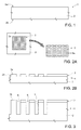
Figure 1 is a schematic cross-sectional view of a micromechanical structure of a MEMS pressure sensor, according to a first embodiment of the present solution, in an initial step of a corresponding manufacturing process; -
Figure 2a is a schematic top plan view of the micromechanical structure in a subsequent step of the manufacturing process; -
Figure 2b is a schematic cross-sectional view corresponding to the top plan view ofFigure 2a ; -
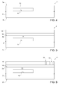
Figures 3-9 are schematic cross-sectional views of the micromechanical structure in subsequent steps of the manufacturing process; -
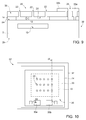
Figure 10 is a schematic top plan view of the micromechanical structure ofFigure 9 ; -
Figure 11 is a schematic cross-sectional view of a micromechanical structure of a MEMS pressure sensor, according to a second embodiment of the present solution, in a final step of a corresponding manufacturing process; -
Figure 12 is a schematic top plan view of the micromechanical structure ofFigure 11 ; -
Figure 13 is a schematic cross-sectional view of a micromechanical structure of a MEMS pressure sensor, according to a third embodiment of the present solution, in a final step of a corresponding manufacturing process; -
Figure 14 is a schematic top plan view of the micromechanical structure ofFigure 13 ; -
Figure 15 shows a graph that compares the plot of the temperature coefficient of a MEMS pressure sensor according to the present solution with that of a piezoresistive pressure sensor of a known type; -
Figure 16 is a general block diagram of an electronic device incorporating the MEMS pressure sensor, according to a further aspect of the present solution; and -
Figure 17 is a general block diagram of a variant embodiment of the MEMS pressure sensor. - With initial reference to
Figure 1 , a manufacturing process is now described for manufacturing a MEMS pressure sensor of a capacitive type, according to one embodiment of the present solution. - In an initial step of the manufacturing process, a
wafer 1 of semiconductor material, for example, monocrystalline silicon, is provided, including asubstrate 2, for example with n-type (or equivalently p-type) doping, and having afront surface 2a and arear surface 2b. - The manufacturing process proceeds with formation of a buried cavity completely contained within the
wafer 1, overlaid by a membrane, with techniques described in detail, for example, inEP 1 324 382 B1 - As illustrated in
Figures 2a and 2b (which are not drawn to scale, as likewise the remaining figures), afirst etching mask 3 is provided on thefront surface 2a of thesubstrate 2, made, for example, of photosensitive material, the so-called "photoresist". - The
first etching mask 3 defines (see the enlarged detail ofFigure 2a ) an etching area, which in the example is approximately square (but may likewise be circular or generically polygonal), and comprises a plurality ofmask portions 3a, for example, hexagonal, which define a lattice, for example, a honeycomb lattice. - As will be evident in what follows, the etching area of the
first etching mask 3 corresponds to the area that will be occupied by the buried cavity and has an extension corresponding to the extension of the membrane that will be formed over the same buried cavity. - Then (see
Figure 3 , which, likeFigure 2b , represents only an enlarged portion of thewafer 1, for reasons of clarity of illustration), using thefirst etching mask 3, an anisotropic chemical etching of thesubstrate 2 is carried out, following upon whichtrenches 6 are formed, which communicate with one another and delimit a plurality of columns 7, made of silicon. - In practice, the
trenches 6 form an open region of a complex shape (corresponding to the lattice of the first etching mask 3) extending in which are the columns 7 (of a shape corresponding to themask portions 3a). - Next, the
first etching mask 3 is removed and an epitaxial growth is carried out in deoxidizing environment (typically, in atmosphere with high hydrogen concentration, preferably with trichlorosilane - SiHCl3). Consequently, an epitaxial layer grows above the columns 7 and closes the aforesaid open region formed by thetrenches 6 at the top. - Then, a step of thermal annealing is carried out, for example, for 30 minutes at 1190°C, preferably in reducing atmosphere, typically in hydrogen atmosphere. The annealing step causes a migration of the silicon atoms, which tend to move into a position of lower energy. Consequently, and also thanks to the short distance between the columns 7, the silicon atoms migrate completely from the portions of the columns 7 present within the aforesaid open region formed by the
trenches 6, and, starting from said region, a buriedcavity 10 is formed. - As shown in
Figure 4 (which represents an enlarged portion of thewafer 1, as compared to that ofFigures 2b and 3 ), a thin silicon layer remains above the buriedcavity 10, constituted in part by silicon atoms grown epitaxially and in part by migrated silicon atoms, and forming amembrane 12, which is flexible and is able to deflect in the presence of external stresses. - In particular, the
membrane 12 separates theburied cavity 10 from thetop surface 2a of thesubstrate 2. The same buriedcavity 10 is separated from therear surface 2b by a thick monolithic region of thesubstrate 2. - Advantageously, during the steps for formation of the
membrane 12 and the buriedcavity 10, dopant atoms may be introduced within thesubstrate 2 and in thesame membrane 12, so as to increase conductivity thereof. - At the end of the manufacturing process steps that have been described previously, the buried
cavity 10 is hence formed within thesubstrate 2, completely contained within thesubstrate 2, being separated both from thefront surface 2a and from therear surface 2b of thesubstrate 2 by continuous portions of material. In yet other words, the buriedcavity 10 has no fluidic communication with the outside of thesubstrate 2. - As shown in
Figure 5 , the manufacturing process then proceeds with the formation on thetop surface 2a of thesubstrate 2, and hence on themembrane 12, of asacrificial layer 14, made, for example, of dielectric material, such as silicon oxide. Thissacrificial layer 14 may, for example, be formed by means of deposition techniques over the entire wafer 1 (the so-called "blank deposition", without the use of masks). - Next, a
conductive layer 15 is formed on thesacrificial layer 14, for example made of polysilicon. In this embodiment, theconductive layer 15 is grown epitaxially on the sacrificial layer 14 (once again without the use of masks). - Then (
Figure 6 ), through a second etching mask (not shown herein), an etching of theconductive layer 15 is carried out, with etch-stop on thesacrificial layer 14, leading to removal of material and to formation of afirst pad trench 16 and of acontact opening 17, both of which traverse theconductive layer 15 throughout its thickness. Thecontact opening 17 is set laterally alongside thefirst pad trench 16, in a more external position with respect to themembrane 12. - Next (
Figure 7 ), the second etching mask is removed and a third etching mask (here not illustrated) is formed above theconductive layer 15, through which an etching of thesacrificial layer 14 is carried out with etch-stop on thesubstrate 2, thus removing a portion of the samesacrificial layer 14 vertically at the contact opening 17, so as to form asecond pad trench 18. - The
second pad trench 18 hence terminates on thetop surface 2a of thesubstrate 2 and is set alongside thefirst pad trench 16, in a position laterally more external with respect to themembrane 12. - Next (
Figure 8 ), the third etching mask is removed, and a deposition mask (here not illustrated) is formed on theconductive layer 15, which coats theconductive layer 15 at an area vertically corresponding to themembrane 12 and instead leaves exposed the first andsecond pad trenches - Using this deposition mask, a
metal region 20, of an appropriate metal material, for example, aluminum (or gold), is then deposited on theconductive layer 15. - In particular, this
metal region 20 fills the first andsecond pad trenches Figure 8 , coming into contact with thetop surface 2a of thesubstrate 2 within thesecond pad trench 18, and with thesacrificial layer 14 within thefirst pad trench 16. - Next (
Figure 9 ), a fourth etching mask (here not illustrated) is formed on theconductive layer 15 and themetal region 20, through which an etching is carried out, with etch-stop first on thesacrificial layer 14, which leads to removal of material and formation of a plurality ofholes 22, which traverse theconductive layer 15 throughout its thickness vertically in a position corresponding to the membrane 12 (for example, theholes 22, of a through type, are formed according to a lattice arrangement, as will be illustrated hereinafter). - Etching, for example a chemical wet etching, then proceeds in the underlying
sacrificial layer 14 through theholes 22, with etch-stop on thetop surface 2a of thesubstrate 2, leading to removal of the material of thesacrificial layer 14 and to formation of anempty space 24, above themembrane 12. - In particular, this
empty space 24 sets in fluidic communication themembrane 12 with the external environment, via theholes 22 that pass through theconductive layer 15. Theholes 22 have in fact a first end 22a, in fluidic communication with the outside world, and a second end 22b, in fluidic communication with theempty space 24 above themembrane 12. - Through the same fourth etching mask, etching (first of the
metal region 20 and of theconductive layer 15, and then of the sacrificial layer 14) leads to formation of aseparation opening 29, which traverses the entire thickness of themetal region 20, of theconductive layer 15, and of thesacrificial layer 14 until thetop surface 2a of thesubstrate 2 is reached. - The
separation opening 29 is set in a position intermediate between the positions previously assumed by the aforesaid first andsecond pad trenches conductive layer 15, aplate region 30, overlying theempty space 24 and themembrane 12; and moreover, starting from themetal region 20, twodistinct pads first pad 30a, set in contact with thesubstrate 2, inside what constituted thesecond pad trench 18, and asecond pad 30b, set in contact with theplate region 30, inside what constituted thefirst pad trench 16. - The manufacturing process then terminates with a step of sawing of the
wafer 1, for definition of dies 32, each die 32 comprising a body of semiconductor material 34 (constituted by a monolithic portion of thesubstrate 2 deriving from sawing of the wafer 1), in which the micromechanical structure, designated as a whole by 35, of the MEMS pressure sensor is integrated. -
Figure 10 is a schematic top plan view of the samemicromechanical structure 35, at the end of the manufacturing process; this top plan view shows in particular the lattice (or array) arrangement of theholes 22 made through theplate region 30. - In detail, the
micromechanical structure 35 thus comprises: the buriedcavity 10, completely contained within the body madesemiconductor material 34, and themembrane 12, which is set above the buriedcavity 10 and separates the same buriedcavity 10 from thetop surface 2a of the body ofsemiconductor material 34; theempty space 24, above themembrane 12, which enables deformation thereof in the presence of incident pressure waves; theplate region 30, set vertically above themembrane 12, from which it is separated by theempty space 24, with the correspondingholes 22 that set the same empty space 24 (and the membrane 12) in communication with the environment external to the MEMS pressure sensor and hence enable entry of the aforesaid pressure waves; and moreover thefirst pad 30a, which electrically contacts the body of semiconductor material 34 (and hence the membrane 12), and thesecond pad 30b, which electrically contacts theplate region 30. - In particular, the
micromechanical structure 35 defines a sensing capacitor C (shown schematically inFigure 9 ) having, as a first plate or electrode, the plate region 30 (hence constituted by an epitaxial polysilicon region released from the underlying substrate), and, as second plate, themembrane 12, the first and second plates being separated by the empty space 24 (which constitutes the dielectric of the sensing capacitor C). - During operation, the pressure exerted by the external environment on the
membrane 12 causes deformation thereof and a capacitance variation of the sensing capacitor C. This capacitance variation may be detected through electrical connection to the first andsecond pads - With reference to
Figures 11 and 12 , a second embodiment of the MEMS capacitive pressure sensor is now described. - In this second embodiment, the
plate region 30 does not haveholes 22 for setting themembrane 12 in fluidic communication with the external environment; thesame plate region 30 is indeed constituted by a solid region without any openings. - In other words, the
empty space 24 is in this case isolated from the external environment, closed between theplate region 30, at the top, and themembrane 12, at the bottom (being moreover delimited laterally by the portions of thesacrificial layer 14, which remain after chemical etching for release of the plate region 30). - The present Applicant has in fact realized that, at least in some applications, it may be disadvantageous for the
membrane 12 to be in direct communication with the external environment. It may in fact be useful to protect themembrane 12 from contaminants, impurities, and/or humidity. - The manufacturing process envisages, in this case, that the holes 22 (once again provided for release of the
plate region 30 by removal via chemical etching of the underlying sacrificial layer 14) are afterwards filled by means of a step of thermal oxidation of thewafer 1, which leads to formation of a coating layer, designated by 36 inFigure 11 , on the exposed surfaces of theconductive layer 15. In particular, thiscoating layer 36 completely fills theholes 22. - In this second embodiment, fluidic communication of the
membrane 12 with the environment external to the body ofsemiconductor material 34 of themicromechanical structure 35 is ensured by a buriedaccess channel 37, which laterally connects up to the buriedcavity 10 within the body ofsemiconductor material 34. - In particular, the buried
access channel 37 extends at a depth, parallel to the top surface of the body ofsemiconductor material 34, and has afirst opening 37a in fluidic communication with the buriedcavity 10 and asecond opening 37b that gives out onto the external environment at a side wall 34' of the body of semiconductor material 34 (this side wall 34' extending transverse to the front and rear surfaces of the body of semiconductor material 34). - The buried
access channel 37 is formed with the same process steps that lead to formation of the buriedcavity 10. - In particular, the mask 3 (described previously with reference to
Figures 2a and 2b ) has in this case a lateral prolongation having the desired conformation for the buriedaccess channel 37, and moreover the step of sawing of thewafer 1 is carried out in such a way that the scribe lines define the aforesaidsecond opening 37b of the buriedaccess channel 37, so as to open the buriedaccess channel 37 onto the external environment. - In this second embodiment, the pressure waves hence enter the buried
access channel 37 from thesecond opening 37b and impinge upon an internal surface of themembrane 12, set in contact with the buriedcavity 10, causing deformation thereof and capacitive variation of the sensing capacitor C (which is, apart from this difference, formed in a way altogether similar to what has been described for the first embodiment). - With reference to
Figures 13 and 14 , a third embodiment of the MEMS pressure sensor of a capacitive type is now described. - In this third embodiment, the
micromechanical structure 32 comprises a reference structure, integrated in the same body ofsemiconductor material 34 where the structure for detecting the pressure of the external environment is formed; the reference structure is designed to allow pressure detection of a differential type (i.e., with respect to a known pressure reference, having characteristics of invariability with respect to the pressure to be detected). - In the third embodiment, the pressure-sensing structure, designated by 38a, is provided in a way altogether similar to the
micromechanical structure 35 discussed in detail previously with reference toFigures 9 and 10 (i.e., it has theholes 22 through theplate region 30 to put themembrane 12 in fluidic communication with the outside world). - The reference structure, designated by 38b, comprises a micromechanical structure, which is also altogether similar to the
micromechanical structure 35, except for the fact that it does not comprise the buriedcavity 10 and themembrane 12. - In particular, this
reference structure 38b comprises: a respective plate region 30', made of conductive material, suspended above asurface portion 34a of the body ofsemiconductor material 34 set laterally with respect to themembrane 12 of thesensing structure 38a, and separated from thesame surface portion 34a by a respective empty space 24'; a plurality of respective holes 22' through the respective plate region 30' for fluidic communication of the respective empty space 24' with the external environment; andrespective pads 30a', 30b', for electrical connection, from outside, of theaforesaid surface portion 34a and of the respective plate region 30', which form the plates of a reference capacitor Cref. - The value of capacitance of the reference capacitor Cref is hence not affected by the pressure to be detected (in so far as the
surface portion 34a of the body ofsemiconductor material 34 does not undergo deformation as a function of this pressure), and is instead affected by the same phenomena of disturbance that afflict thesensing structure 38a, for example, in the presence of humidity. - The corresponding manufacturing process hence envisages altogether similar process steps (carried out simultaneously) for providing the
sensing structure 38a and thereference structure 38b, except for the absence of the initial steps of formation of a buried cavity for thereference structure 38b. - The ASIC associated to the micromechanical structures receives in this case the capacitive variations both of the sensing capacitor C and of the reference capacitor Cref by means of the first and
second pads sensing structure 38a, and by means of similar first andsecond pads 30a', 30b' of thereference structure 38b. - The ASIC advantageously processes these capacitive variations of the sensing capacitor C and of the reference capacitor Cref in a differential way so as to eliminate the effects of the disturbance, for example, due to humidity, on the detected pressure value.
- As shown in
Figure 13 , a dopedregion 39, 39' may moreover be present both in thesensing structure 38a and in thereference structure 38b, in a surface portion of the body ofsemiconductor material 34 underneath theempty space 24, 24' (set in a position corresponding to themembrane 12, for the sensing structure 35a, and forming a surface portion of the same membrane 12). - The doped
region 39, 39' may be formed by implantation or diffusion of dopants through a dedicated mask, following upon formation of the buriedcavity 10, and in this case contributes to constituting the second plate of the sensing capacitor C and reference capacitor Cref; advantageously, the presence of this dopedregion 39, 39' enables increase of the conductivity of the aforesaid second plate and improves the sensing characteristics. - The advantages of the solution described emerge clearly from the foregoing description.
- In particular, the MEMS pressure sensor, which is based upon the principle of capacitive detection, has a variability and a non-linearity with respect to temperature, that are much lower than those of known solutions, based on the piezoresistive sensing principle.
- In this regard,
Figure 15 compares the plot of the thermal coefficient TCO (expressed as percentage of the full scale FS) of the pressure sensor according to the present solution, of a capacitive type, with the temperature coefficient TCO' of a known pressure sensor, of a piezoresistive type. - From a comparison of the plots, the higher stability in temperature of the MEMS pressure sensor according to the present solution is evident, as likewise the greater linearity of its response.
- In particular, the present Applicant has found for the MEMS pressure sensor according to the present solution a temperature coefficient TCO of 0.4 mbar/°C (i.e., 0.04% FS/°C) as against a temperature coefficient TCO' of 2 mbar/°C (i.e., 0.2% FS/°C) for the known pressure sensor.
- The process for manufacturing the MEMS pressure sensor according to the present solution is advantageously less complex and less costly than that of pressure sensors of a known type, in particular of a piezoresistive type, thanks, for example, to the absence of masks dedicated to the processes of diffusion of the corresponding piezoresistive elements.
- In particular, the present Applicant has noted a reduction of the number of masks required by the manufacturing process, which may, for example, be only five in the embodiments described (four etching masks and one deposition mask), as against processes for manufacturing piezoresistive pressure sensors, which require, for example, nine masks.
- Furthermore, the solution described advantageously enables a simple and effective implementation of self-test operations in the MEMS pressure sensor, for example, by applying from outside appropriate electrical biasing signals to the plates of the sensing capacitor C by means of the first and
second pads - In general, the aforesaid characteristics render use of the MEMS pressure sensor in an
electronic device 50 particularly advantageous, for example, for barometric applications in the automotive field, as shown schematically inFigure 16 . - In particular, in
Figure 16 , the MEMS pressure sensor is designated by 42, including themicromechanical structure 35 described previously and anASIC 43, which provides the corresponding reading interface (and may be provided in thesame die 32 as that of themicromechanical structure 35, or in a different die, which may in any case be housed in one and the same package). - The
electronic device 50 is generally able to process, store, and/or transmit and receive signals and information, and comprises: amicroprocessor 44, which receives the signals detected by theMEMS pressure sensor 42; an input/output interface 45 connected to themicroprocessor 44; and aninternal memory 46, of a non-volatile type. - The
electronic device 50, when used in the automotive field, may, for example, control the air/fuel mixture for combustion in the engine, or else control opening of an airbag, as a function the detected pressure value. - Finally, it is clear that modifications and variations may be made to what has been described and illustrated herein, without thereby departing from the scope of the present invention, as defined in the annexed claims.
- In particular, it is evident that modifications may be made to the materials used for manufacturing the
MEMS pressure sensor 42, it being possible, for example, for a different metal material to be used for providing thepads sacrificial layer 14. - In addition, it is evident that the
MEMS pressure sensor 42 may advantageously be used also for different applications, where it is desired to obtain a detection of pressure with characteristics of independence from temperature, for example, in portable or wearable devices (such as smartphones, tablets, smartwatches, or the like), or in industrial applications, where high temperatures are reached (for example, in the range from -40°C to 175°C). - Moreover, the MEMS pressure sensor may advantageously be integrated with further MEMS inertial sensors and/or microphones, thanks to the compatibility of the manufacturing process used.
- In this regard,
Figure 17 is a schematic illustration of a combined MEMS sensor, designated by 62, including a micromechanical sensing structure of a combined type, designated by 64, which integrates, advantageously in one and the same body of semiconductor material, themicromechanical structure 35 described previously in detail for pressure detection, and moreover a furthermicromechanical sensing structure 65, of a known type, for example, for detecting an acceleration, an angular velocity, or acoustic waves. Themicromechanical structures - The combined
MEMS sensor 62 further comprises an ASIC, once again designated by 43, operatively coupled both to themicromechanical structure 35 and to the furthermicromechanical sensing structure 65, in order to provide a combined sensing structure (i.e., an accelerometer, a gyroscope, or a microphone, combined with the pressure sensor).
Claims (18)
- A process for manufacturing a MEMS pressure sensor (42) having a micromechanical structure (35) comprising:providing a wafer (1) including a substrate (2) of semiconductor material and having a top surface (2a);forming a buried cavity (10) entirely contained within said substrate (2) and separated from said top surface (2a) by a membrane (12), suspended above said buried cavity (10) ;forming a fluidic-communication access (22; 37), for fluidic communication of said membrane (12) with an external environment, set at a pressure the value of which has to be determined;forming, suspended above said membrane (12), a plate region (30), made of conductive material, separated from said membrane (12) by an empty space (24); andforming electrical-contact elements (30a, 30b), for electrical connection of said membrane (12) and said plate region (30), which are designed to form the plates of a sensing capacitor (C), the value of capacitance of which is indicative of the value of pressure to be detected.
- The process according to claim 1, wherein said step of forming a buried cavity (10) comprises the steps of:forming within said substrate (2), starting from the top surface (2a), trenches (6) that delimit between them columns (7) of semiconductor material;epitaxially growing, starting from said columns (7), a closing layer of semiconductor material, said closing layer closing the trenches (6) at the top; andcarrying out a thermal treatment such as to cause migration of the semiconductor material of said columns (7) towards said closing layer, to form said buried cavity (10) and said membrane (12) suspended above said buried cavity (10).
- The process according to claim 1 or 2, wherein forming a plate region (30) comprises, after formation of said buried cavity (10), the steps of:forming a sacrificial layer (14) on the top surface (2a) of said substrate (2);forming a conductive layer (15) on the sacrificial layer (14);opening a number of holes (22) through said conductive layer (15), in a position vertically corresponding to said membrane (12); andpartially removing said sacrificial layer (14) through said holes (22) so as to release said conductive layer (15) with respect to the substrate (2), to form said plate region (30) and said empty space (24) above said membrane (12).
- The process according to claim 3, wherein forming a conductive layer (15) comprises epitaxially growing said conductive layer (15) on the sacrificial layer (14); and wherein said conductive layer (15) comprises polysilicon.
- The process according to claim 3 or 4, wherein forming a fluidic-communication access (22) of said membrane (12) towards the external environment comprises forming said holes (22) through the conductive layer (15), said holes (22) having a first end (22a) in fluidic communication with the outside, and a second end (22b) in fluidic communication with said empty space (24) above said membrane (12).
- The process according to claim 3 or 4, further comprising filling completely said holes (22) with a filler layer (36); and wherein forming a fluidic-communication access (37) of said membrane (12) towards the external environment comprises:forming a buried access channel (37), which is contained within said substrate (2), at a distance from said front surface (2a), and has a first opening (37a) in fluidic communication with said buried cavity (10); andcarrying out an operation of sawing of said wafer (1) into dies (32), each comprising a body of semiconductor material (34) obtained starting from said substrate (2), in such a way as to define a second opening (37b) of said buried access channel (37) giving out onto the external environment at an outer side wall (34') of said body of semiconductor material (34).
- The process according to claim 6, wherein forming a buried access channel (37) is performed simultaneously with said step of forming a buried cavity (10).
- The process according to any one of claims 3-7, wherein forming electrical-contact elements (30a, 30b) comprises:forming a first contact trench (16) through said conductive layer (15) until said sacrificial layer (14) is reached;forming a second contact trench (18) through said conductive layer (15) and said sacrificial layer (14), until the top surface (2a) of said substrate (2) is reached;forming a conductive region (20) above said conductive layer (15) and within said first contact trench (16) and said second contact trench (18);defining, by etching, said conductive region (20) so as to form a first electrical-contact element (30a), for electrical connection, from outside, of said membrane (12), and a second electrical-contact element (30b), for electrical connection, from outside, of said plate region (30).
- The process according to any one of the preceding claims, further comprising forming a reference structure (38b), in addition to a pressure-sensing structure (38a) of said micromechanical structure (35), within said wafer (1).
- A MEMS pressure sensor (42) having a micromechanical structure (35) comprising:a body (34) including semiconductor material and having a top surface (2a);a buried cavity (10) entirely contained within said body (34) and separated from said top surface (2a) by a membrane (12), suspended above said buried cavity (10);a fluidic-communication access (22; 37), for fluidic communication of said membrane (12) with an external environment, set at a pressure the value of which has to be determined;a plate region (30), made of conductive material, suspended above said membrane (12) and separated from said membrane (12) by an empty space (24); andelectrical-contact elements (30a, 30b), for electrical connection of said membrane (12) and of said plate region (30), which are designed to form the plates of a sensing capacitor (C), the value of capacitance of which is indicative of the value of pressure to be detected.
- The sensor according to claim 10, wherein said plate region (30) comprises a layer of epitaxial polysilicon grown above the top surface (2a) of said body (34).
- The sensor according to claim 10 or 11, wherein said fluidic-communication access of said membrane (12) towards the external environment comprises a number of holes (22) made through the plate region (30), said holes (22) having a first end (22a) in fluidic communication with the outside, and a second end (22b) in fluidic communication with said empty space (24) above said membrane (12).
- The sensor according to claim 10 or 11, wherein said fluidic-communication access of said membrane (12) towards the external environment comprises a buried access channel (37), which is contained within said body (34), at a distance from said front surface (2a), and has a first opening (37a) in fluidic communication with said buried cavity (10) and a second opening (37b) giving out onto the external environment at an outer side wall (34') of said body (34).
- The sensor according to any one of claims 10-13, wherein said electrical-contact elements (30a, 30b) comprise: a first electrical-contact element (30a), electrically connected to said membrane (12), and a second electrical-contact element (30b), electrically connected to said plate region (30); said first electrical-contact element (30a) and said second electrical-contact element (30b) being separated by a separation trench (29).
- The sensor according to any one of claims 10-14, wherein said micromechanical structure (35) further comprises a reference structure (38b), in addition to a pressure-sensing structure (38a), within said body (34).
- The sensor according to claim 15, wherein said reference structure (38b) comprises:a respective plate region (30'), made of conductive material, suspended above a surface portion (34a) of said body (34) set laterally with respect to said membrane (12) and separated from said surface portion (34a) by a respective empty space (24');a respective fluidic-communication access (22') for fluidic communication of said respective empty space (24') with the external environment;respective electrical-contact elements (30a', 30b') for electrical connection of said surface portion (34a) and of said respective plate region (30'), which are designed to form the plates of a reference capacitor (Cref), the value of capacitance of which is independent of the value of the pressure to be detected.
- The sensor according to any one of claims 10-16, further comprising a doped region (39) set in a surface portion of said membrane (12).
- The sensor according to any one of claims 10-17, further comprising an additional micromechanical sensing structure (65) integrated together with said micromechanical structure (35) for providing a pressure sensor combined with a gyroscope, accelerometer, or microphone.
Applications Claiming Priority (1)
| Application Number | Priority Date | Filing Date | Title |
|---|---|---|---|
| ITUA2016A002174A ITUA20162174A1 (en) | 2016-03-31 | 2016-03-31 | PROCESS OF MANUFACTURE OF A MEMS PRESSURE SENSOR AND RELATIVE MEMS PRESSURE SENSOR |
Publications (2)
| Publication Number | Publication Date |
|---|---|
| EP3225586A1 true EP3225586A1 (en) | 2017-10-04 |
| EP3225586B1 EP3225586B1 (en) | 2019-05-08 |
Family
ID=56235946
Family Applications (1)
| Application Number | Title | Priority Date | Filing Date |
|---|---|---|---|
| EP16194692.6A Active EP3225586B1 (en) | 2016-03-31 | 2016-10-19 | Process for manufacturing a mems pressure sensor, and corresponding mems pressure sensor |
Country Status (4)
| Country | Link |
|---|---|
| US (2) | US10048148B2 (en) |
| EP (1) | EP3225586B1 (en) |
| CN (3) | CN107265395B (en) |
| IT (1) | ITUA20162174A1 (en) |
Families Citing this family (25)
| Publication number | Priority date | Publication date | Assignee | Title |
|---|---|---|---|---|
| ITTO20130502A1 (en) * | 2013-06-18 | 2014-12-19 | St Microelectronics Asia | ELECTRONIC DEVICE WITH INTEGRATED TEMPERATURE SENSOR AND ITS MANUFACTURING METHOD |
| US10753815B2 (en) * | 2015-10-28 | 2020-08-25 | Hewlett-Packard Development Company, L.P. | Relative pressure sensor |
| ITUA20162174A1 (en) * | 2016-03-31 | 2017-10-01 | St Microelectronics Srl | PROCESS OF MANUFACTURE OF A MEMS PRESSURE SENSOR AND RELATIVE MEMS PRESSURE SENSOR |
| DE102017202605A1 (en) * | 2017-02-17 | 2018-08-23 | Robert Bosch Gmbh | Micromechanical arrangement with a sensitive element and associated manufacturing method |
| CN108072477B (en) * | 2017-12-05 | 2020-09-18 | 北京遥测技术研究所 | MEMS (micro-electromechanical system) air pressure sensor and method for improving long-term stability thereof |
| IT201800001092A1 (en) * | 2018-01-16 | 2019-07-16 | St Microelectronics Srl | MICROELECTROMECHANICAL PIEZORESISTIVE PRESSURE SENSOR WITH SELF-DIAGNOSTIC CAPACITY AND RELATED MANUFACTURING PROCESS |
| CN112334867B (en) | 2018-05-24 | 2025-11-11 | 纽约州立大学研究基金会 | Capacitive sensor |
| CN109029828B (en) * | 2018-06-07 | 2019-08-02 | 江苏大学 | A kind of capacitance differential pressure transducer and its output characteristics calculation method and production method |
| CN109141728A (en) * | 2018-07-18 | 2019-01-04 | 江苏大学 | Fixed capacitive pressure transducer and production method among a kind of pressure sensitive film |
| IT201800007442A1 (en) * | 2018-07-23 | 2020-01-23 | PROCESS FOR MANUFACTURING MICROELECTROMECHANICAL DEVICES, IN PARTICULAR ELECTROACOUSTIC MODULES | |
| CN110862063A (en) * | 2018-08-28 | 2020-03-06 | 无锡华润上华科技有限公司 | Temperature sensor preparation method and temperature sensor |
| US11865581B2 (en) * | 2018-11-21 | 2024-01-09 | Stmicroelectronics S.R.L. | Ultrasonic MEMS acoustic transducer with reduced stress sensitivity and manufacturing process thereof |
| DE102018222738A1 (en) * | 2018-12-21 | 2020-06-25 | Robert Bosch Gmbh | Micromechanical pressure sensor device and a corresponding manufacturing method |
| DE102018222758A1 (en) * | 2018-12-21 | 2020-06-25 | Robert Bosch Gmbh | MEMS sensor with a membrane and method for producing a MEMS sensor |
| CN109809355B (en) * | 2019-03-06 | 2025-02-28 | 苏州敏芯微电子技术股份有限公司 | Pressure sensor and method for manufacturing the same |
| JP7147650B2 (en) * | 2019-03-20 | 2022-10-05 | 株式会社デンソー | Semiconductor device and its manufacturing method |
| DE102020200333A1 (en) * | 2020-01-14 | 2021-07-15 | Robert Bosch Gesellschaft mit beschränkter Haftung | Micromechanical component for a sensor or microphone device |
| IT202000011755A1 (en) * | 2020-05-20 | 2021-11-20 | St Microelectronics Srl | MANUFACTURING PROCESS OF A MICRO-ELECTRO-MECHANICAL DEVICE, IN PARTICULAR MOVEMENT SENSOR WITH CAPACITIVE COMMAND/DETECTION, AND RELATED MEMS DEVICE |
| CN112357875B (en) * | 2020-11-06 | 2023-12-26 | 杭州士兰微电子股份有限公司 | MEMS sensor and preparation method thereof |
| IT202100019718A1 (en) | 2021-07-23 | 2023-01-23 | St Microelectronics Srl | IMPROVED PROCESS FOR MANUFACTURING ELECTROACOUSTIC MODULES |
| IT202100022511A1 (en) | 2021-08-30 | 2023-03-02 | St Microelectronics Srl | PROCESS OF MANUFACTURING AN INTEGRATED SYSTEM INCLUDING A CAPACITIVE PRESSURE SENSOR AND AN INERTIAL SENSOR, AND INTEGRATED SYSTEM |
| CN218491481U (en) * | 2021-08-30 | 2023-02-17 | 意法半导体股份有限公司 | Semiconductor device with a plurality of transistors |
| DE102022201813A1 (en) | 2022-02-22 | 2023-08-24 | Robert Bosch Gesellschaft mit beschränkter Haftung | Method for forming a layer structure surrounding at least one recess and device with a layer structure |
| JP2024002882A (en) * | 2022-06-24 | 2024-01-11 | ローム株式会社 | Pressure sensor and pressure sensor manufacturing method |
| CN118329243A (en) * | 2024-04-28 | 2024-07-12 | 广东人工智能与先进计算研究院 | A pressure sensor array module and a method for preparing the same |
Citations (3)
| Publication number | Priority date | Publication date | Assignee | Title |
|---|---|---|---|---|
| EP1324382B1 (en) | 2001-12-28 | 2007-03-07 | STMicroelectronics S.r.l. | Process for manufacturing an SOI wafer by annealing and oxidation of buried channels |
| US20120043627A1 (en) * | 2010-08-23 | 2012-02-23 | Freescale Semiconductor, Inc. | MEMS Sensor Device With Multi-Stimulus Sensing and Method of Fabricating Same |
| EP2423157A2 (en) * | 2010-08-23 | 2012-02-29 | Freescale Semiconductor, Inc. | MEMS pressure sensor device and method of fabricating same |
Family Cites Families (39)
| Publication number | Priority date | Publication date | Assignee | Title |
|---|---|---|---|---|
| US5332469A (en) * | 1992-11-12 | 1994-07-26 | Ford Motor Company | Capacitive surface micromachined differential pressure sensor |
| US5369544A (en) * | 1993-04-05 | 1994-11-29 | Ford Motor Company | Silicon-on-insulator capacitive surface micromachined absolute pressure sensor |
| US5427975A (en) * | 1993-05-10 | 1995-06-27 | Delco Electronics Corporation | Method of micromachining an integrated sensor on the surface of a silicon wafer |
| US5747705A (en) * | 1996-12-31 | 1998-05-05 | Honeywell Inc. | Method for making a thin film resonant microbeam absolute |
| EP1577656B1 (en) * | 2004-03-19 | 2010-06-09 | STMicroelectronics Srl | Method for manufacturing a semiconductor pressure sensor |
| US7240560B2 (en) * | 2004-10-18 | 2007-07-10 | Silverbrook Research Pty Ltd | Pressure sensor with remote power source |
| US7194901B2 (en) * | 2004-10-18 | 2007-03-27 | Silverbrook Research Pty Ltd | Pressure sensor with apertured membrane guard |
| US8053823B2 (en) * | 2005-03-08 | 2011-11-08 | International Business Machines Corporation | Simplified buried plate structure and process for semiconductor-on-insulator chip |
| JP5174673B2 (en) * | 2005-10-14 | 2013-04-03 | エスティーマイクロエレクトロニクス エス.アール.エル. | Electronic device with substrate level assembly and method of manufacturing the same |
| DE102005060855A1 (en) * | 2005-12-20 | 2007-06-28 | Robert Bosch Gmbh | Micromechanical capacitive pressure transducer and manufacturing process |
| DE102006028435A1 (en) * | 2006-06-21 | 2007-12-27 | Robert Bosch Gmbh | Sensor and method for its production |
| JP4215076B2 (en) * | 2006-07-10 | 2009-01-28 | ヤマハ株式会社 | Condenser microphone and manufacturing method thereof |
| US20080015494A1 (en) * | 2006-07-11 | 2008-01-17 | Microchips, Inc. | Multi-reservoir pump device for dialysis, biosensing, or delivery of substances |
| ITTO20070190A1 (en) * | 2007-03-14 | 2008-09-15 | St Microelectronics Srl | PROCESS OF MANUFACTURING OF A MEMBRANE OF SEMICONDUCTOR MATERIAL INTEGRATED IN, AND ISOLATED ELECTRICALLY BY, A SUBSTRATE |
| US8193596B2 (en) * | 2008-09-03 | 2012-06-05 | Solid State System Co., Ltd. | Micro-electro-mechanical systems (MEMS) package |
| KR101158044B1 (en) * | 2008-12-03 | 2012-06-22 | 한국전자통신연구원 | The high sensitivity Z-axis vibration detection sensor and Method for fabricating thereof |
| IT1395550B1 (en) * | 2008-12-23 | 2012-09-28 | St Microelectronics Rousset | INTEGRATED ACOUSTIC TRANSDUCER IN MEMS TECHNOLOGY AND RELATIVE PROCESS OF PROCESSING |
| ITTO20090616A1 (en) * | 2009-08-05 | 2011-02-06 | St Microelectronics Srl | PROCESS OF MANUFACTURING OF MEMS DEVICES EQUIPPED WITH CUTTED CAVITIES AND MEMS DEVICE SO OBTAINED |
| DE102010064120B4 (en) * | 2010-12-23 | 2023-05-25 | Robert Bosch Gmbh | Component and method for its manufacture |
| JP5649474B2 (en) * | 2011-01-26 | 2015-01-07 | ローム株式会社 | Capacitance type pressure sensor and method of manufacturing capacitance type pressure sensor |
| US20130001710A1 (en) * | 2011-06-29 | 2013-01-03 | Invensense, Inc. | Process for a sealed mems device with a portion exposed to the environment |
| US8687827B2 (en) * | 2012-05-29 | 2014-04-01 | Merry Electronics Co., Ltd. | Micro-electro-mechanical system microphone chip with expanded back chamber |
| EP2892725B1 (en) * | 2012-09-12 | 2017-03-08 | Funai Electric Co., Ltd. | Maintenance valve for fluid ejection head |
| GB2506174A (en) * | 2012-09-24 | 2014-03-26 | Wolfson Microelectronics Plc | Protecting a MEMS device from excess pressure and shock |
| US9726563B2 (en) * | 2012-09-25 | 2017-08-08 | The University Of Tokyo | Device member including cavity and method of producing the device member including cavity |
| US8921952B2 (en) * | 2013-01-29 | 2014-12-30 | Freescale Semiconductor Inc. | Microelectromechanical system devices having crack resistant membrane structures and methods for the fabrication thereof |
| US9676614B2 (en) * | 2013-02-01 | 2017-06-13 | Analog Devices, Inc. | MEMS device with stress relief structures |
| DE102013217726B4 (en) * | 2013-09-05 | 2021-07-29 | Robert Bosch Gmbh | Micromechanical component for a capacitive sensor device and manufacturing method for a micromechanical component for a capacitive sensor device |
| EP2887387A1 (en) * | 2013-12-20 | 2015-06-24 | Nxp B.V. | Semiconductor device and associated method |
| CN103712720B (en) * | 2014-01-02 | 2015-08-19 | 杭州士兰集成电路有限公司 | Capacitance pressure transducer, and inertial sensor integrated device and forming method thereof |
| DE102014200500A1 (en) * | 2014-01-14 | 2015-07-16 | Robert Bosch Gmbh | Micromechanical pressure sensor device and corresponding manufacturing method |
| US9114976B1 (en) * | 2014-03-07 | 2015-08-25 | Taiwan Semiconductor Manufacturing Company Limited | Semiconductor arrangement with stress release configuration |
| CN105222931B (en) * | 2014-06-25 | 2019-02-19 | 香港科技大学 | MEMS capacitive pressure sensor and its manufacturing method |
| US10023461B2 (en) * | 2014-10-31 | 2018-07-17 | Stmicroelectronics S.R.L. | Microintegrated encapsulated MEMS sensor with mechanical decoupling and manufacturing process thereof |
| CN104883652B (en) * | 2015-05-29 | 2019-04-12 | 歌尔股份有限公司 | MEMS microphone, pressure sensor integrated morphology and its manufacturing method |
| CN107850505A (en) * | 2015-06-15 | 2018-03-27 | 芬兰国家技术研究中心股份公司 | MEMS capacitive pressure sensor and manufacture method |
| CN205262665U (en) * | 2015-06-22 | 2016-05-25 | 意法半导体股份有限公司 | Pressure sensor |
| CN204881959U (en) * | 2015-06-29 | 2015-12-16 | 歌尔声学股份有限公司 | MEMS pressure sensing component |
| ITUA20162174A1 (en) * | 2016-03-31 | 2017-10-01 | St Microelectronics Srl | PROCESS OF MANUFACTURE OF A MEMS PRESSURE SENSOR AND RELATIVE MEMS PRESSURE SENSOR |
-
2016
- 2016-03-31 IT ITUA2016A002174A patent/ITUA20162174A1/en unknown
- 2016-09-26 US US15/276,617 patent/US10048148B2/en active Active
- 2016-09-29 CN CN201610868540.0A patent/CN107265395B/en active Active
- 2016-09-29 CN CN202010562184.6A patent/CN111704104B/en active Active
- 2016-09-29 CN CN201621095937.2U patent/CN206126837U/en not_active Withdrawn - After Issue
- 2016-10-19 EP EP16194692.6A patent/EP3225586B1/en active Active
-
2018
- 2018-04-20 US US15/958,461 patent/US10578505B2/en active Active
Patent Citations (3)
| Publication number | Priority date | Publication date | Assignee | Title |
|---|---|---|---|---|
| EP1324382B1 (en) | 2001-12-28 | 2007-03-07 | STMicroelectronics S.r.l. | Process for manufacturing an SOI wafer by annealing and oxidation of buried channels |
| US20120043627A1 (en) * | 2010-08-23 | 2012-02-23 | Freescale Semiconductor, Inc. | MEMS Sensor Device With Multi-Stimulus Sensing and Method of Fabricating Same |
| EP2423157A2 (en) * | 2010-08-23 | 2012-02-29 | Freescale Semiconductor, Inc. | MEMS pressure sensor device and method of fabricating same |
Also Published As
| Publication number | Publication date |
|---|---|
| US20180299337A1 (en) | 2018-10-18 |
| US20170284882A1 (en) | 2017-10-05 |
| ITUA20162174A1 (en) | 2017-10-01 |
| CN107265395A (en) | 2017-10-20 |
| US10048148B2 (en) | 2018-08-14 |
| EP3225586B1 (en) | 2019-05-08 |
| CN111704104A (en) | 2020-09-25 |
| US10578505B2 (en) | 2020-03-03 |
| CN107265395B (en) | 2020-07-21 |
| CN206126837U (en) | 2017-04-26 |
| CN111704104B (en) | 2025-06-20 |
Similar Documents
| Publication | Publication Date | Title |
|---|---|---|
| US10578505B2 (en) | Process for manufacturing a MEMS pressure sensor, and corresponding MEMS pressure sensor | |
| US10962431B2 (en) | Pressure sensor generating a transduced signal with reduced ambient temperature dependence, and manufacturing method thereof | |
| US11054327B2 (en) | Microelectromechanical piezoresistive pressure sensor with self-test capability and corresponding manufacturing process | |
| US8387464B2 (en) | Laterally integrated MEMS sensor device with multi-stimulus sensing | |
| US8008738B2 (en) | Integrated differential pressure sensor | |
| US8487387B2 (en) | MEMS sensor device with multi-stimulus sensing | |
| US8575710B2 (en) | Capacitive semiconductor pressure sensor | |
| US10150666B2 (en) | Micro-electro-mechanical device and manufacturing process thereof | |
| JP4298807B2 (en) | Integrated piezoresistive pressure sensor and method of manufacturing the same | |
| KR101921843B1 (en) | Suspended membrane for capacitive pressure sensor | |
| JP2004513356A (en) | Absolute pressure sensor with fine surface processing and its manufacturing method | |
| WO2002004907A1 (en) | Surface-micromachined pressure sensor and high pressure application | |
| EP0672898A2 (en) | Semiconductor pressure sensor with polysilicon diaphragm and single-crystal gage elements and fabrication method therefor | |
| US9330929B1 (en) | Systems and methods for horizontal integration of acceleration sensor structures | |
| CN109809355B (en) | Pressure sensor and method for manufacturing the same | |
| US20250189392A1 (en) | Microelectromechanical sensor with external fluidic coupling having contamination-reducing structure |
Legal Events
| Date | Code | Title | Description |
|---|---|---|---|
| PUAI | Public reference made under article 153(3) epc to a published international application that has entered the european phase |
Free format text: ORIGINAL CODE: 0009012 |
|
| STAA | Information on the status of an ep patent application or granted ep patent |
Free format text: STATUS: THE APPLICATION HAS BEEN PUBLISHED |
|
| AK | Designated contracting states |
Kind code of ref document: A1 Designated state(s): AL AT BE BG CH CY CZ DE DK EE ES FI FR GB GR HR HU IE IS IT LI LT LU LV MC MK MT NL NO PL PT RO RS SE SI SK SM TR |
|
| AX | Request for extension of the european patent |
Extension state: BA ME |
|
| STAA | Information on the status of an ep patent application or granted ep patent |
Free format text: STATUS: REQUEST FOR EXAMINATION WAS MADE |
|
| 17P | Request for examination filed |
Effective date: 20180403 |
|
| RBV | Designated contracting states (corrected) |
Designated state(s): AL AT BE BG CH CY CZ DE DK EE ES FI FR GB GR HR HU IE IS IT LI LT LU LV MC MK MT NL NO PL PT RO RS SE SI SK SM TR |
|
| GRAP | Despatch of communication of intention to grant a patent |
Free format text: ORIGINAL CODE: EPIDOSNIGR1 |
|
| STAA | Information on the status of an ep patent application or granted ep patent |
Free format text: STATUS: GRANT OF PATENT IS INTENDED |
|
| INTG | Intention to grant announced |
Effective date: 20181108 |
|
| GRAJ | Information related to disapproval of communication of intention to grant by the applicant or resumption of examination proceedings by the epo deleted |
Free format text: ORIGINAL CODE: EPIDOSDIGR1 |
|
| STAA | Information on the status of an ep patent application or granted ep patent |
Free format text: STATUS: REQUEST FOR EXAMINATION WAS MADE |
|
| GRAS | Grant fee paid |
Free format text: ORIGINAL CODE: EPIDOSNIGR3 |
|
| STAA | Information on the status of an ep patent application or granted ep patent |
Free format text: STATUS: GRANT OF PATENT IS INTENDED |
|
| GRAP | Despatch of communication of intention to grant a patent |
Free format text: ORIGINAL CODE: EPIDOSNIGR1 |
|
| GRAA | (expected) grant |
Free format text: ORIGINAL CODE: 0009210 |
|
| STAA | Information on the status of an ep patent application or granted ep patent |
Free format text: STATUS: THE PATENT HAS BEEN GRANTED |
|
| INTC | Intention to grant announced (deleted) | ||
| RIC1 | Information provided on ipc code assigned before grant |
Ipc: G01L 9/00 20060101ALI20190314BHEP Ipc: B81C 1/00 20060101AFI20190314BHEP |
|
| INTG | Intention to grant announced |
Effective date: 20190329 |
|
| AK | Designated contracting states |
Kind code of ref document: B1 Designated state(s): AL AT BE BG CH CY CZ DE DK EE ES FI FR GB GR HR HU IE IS IT LI LT LU LV MC MK MT NL NO PL PT RO RS SE SI SK SM TR |
|
| REG | Reference to a national code |
Ref country code: GB Ref legal event code: FG4D |
|
| REG | Reference to a national code |
Ref country code: CH Ref legal event code: EP Ref country code: AT Ref legal event code: REF Ref document number: 1129843 Country of ref document: AT Kind code of ref document: T Effective date: 20190515 |
|
| REG | Reference to a national code |
Ref country code: DE Ref legal event code: R096 Ref document number: 602016013528 Country of ref document: DE Ref country code: IE Ref legal event code: FG4D |
|
| REG | Reference to a national code |
Ref country code: NL Ref legal event code: MP Effective date: 20190508 |
|
| REG | Reference to a national code |
Ref country code: LT Ref legal event code: MG4D |
|
| PG25 | Lapsed in a contracting state [announced via postgrant information from national office to epo] |
Ref country code: FI Free format text: LAPSE BECAUSE OF FAILURE TO SUBMIT A TRANSLATION OF THE DESCRIPTION OR TO PAY THE FEE WITHIN THE PRESCRIBED TIME-LIMIT Effective date: 20190508 Ref country code: NO Free format text: LAPSE BECAUSE OF FAILURE TO SUBMIT A TRANSLATION OF THE DESCRIPTION OR TO PAY THE FEE WITHIN THE PRESCRIBED TIME-LIMIT Effective date: 20190808 Ref country code: AL Free format text: LAPSE BECAUSE OF FAILURE TO SUBMIT A TRANSLATION OF THE DESCRIPTION OR TO PAY THE FEE WITHIN THE PRESCRIBED TIME-LIMIT Effective date: 20190508 Ref country code: ES Free format text: LAPSE BECAUSE OF FAILURE TO SUBMIT A TRANSLATION OF THE DESCRIPTION OR TO PAY THE FEE WITHIN THE PRESCRIBED TIME-LIMIT Effective date: 20190508 Ref country code: PT Free format text: LAPSE BECAUSE OF FAILURE TO SUBMIT A TRANSLATION OF THE DESCRIPTION OR TO PAY THE FEE WITHIN THE PRESCRIBED TIME-LIMIT Effective date: 20190908 Ref country code: SE Free format text: LAPSE BECAUSE OF FAILURE TO SUBMIT A TRANSLATION OF THE DESCRIPTION OR TO PAY THE FEE WITHIN THE PRESCRIBED TIME-LIMIT Effective date: 20190508 Ref country code: NL Free format text: LAPSE BECAUSE OF FAILURE TO SUBMIT A TRANSLATION OF THE DESCRIPTION OR TO PAY THE FEE WITHIN THE PRESCRIBED TIME-LIMIT Effective date: 20190508 Ref country code: HR Free format text: LAPSE BECAUSE OF FAILURE TO SUBMIT A TRANSLATION OF THE DESCRIPTION OR TO PAY THE FEE WITHIN THE PRESCRIBED TIME-LIMIT Effective date: 20190508 Ref country code: LT Free format text: LAPSE BECAUSE OF FAILURE TO SUBMIT A TRANSLATION OF THE DESCRIPTION OR TO PAY THE FEE WITHIN THE PRESCRIBED TIME-LIMIT Effective date: 20190508 |
|
| PG25 | Lapsed in a contracting state [announced via postgrant information from national office to epo] |
Ref country code: BG Free format text: LAPSE BECAUSE OF FAILURE TO SUBMIT A TRANSLATION OF THE DESCRIPTION OR TO PAY THE FEE WITHIN THE PRESCRIBED TIME-LIMIT Effective date: 20190808 Ref country code: RS Free format text: LAPSE BECAUSE OF FAILURE TO SUBMIT A TRANSLATION OF THE DESCRIPTION OR TO PAY THE FEE WITHIN THE PRESCRIBED TIME-LIMIT Effective date: 20190508 Ref country code: GR Free format text: LAPSE BECAUSE OF FAILURE TO SUBMIT A TRANSLATION OF THE DESCRIPTION OR TO PAY THE FEE WITHIN THE PRESCRIBED TIME-LIMIT Effective date: 20190809 Ref country code: LV Free format text: LAPSE BECAUSE OF FAILURE TO SUBMIT A TRANSLATION OF THE DESCRIPTION OR TO PAY THE FEE WITHIN THE PRESCRIBED TIME-LIMIT Effective date: 20190508 |
|
| REG | Reference to a national code |
Ref country code: AT Ref legal event code: MK05 Ref document number: 1129843 Country of ref document: AT Kind code of ref document: T Effective date: 20190508 |
|
| PG25 | Lapsed in a contracting state [announced via postgrant information from national office to epo] |
Ref country code: EE Free format text: LAPSE BECAUSE OF FAILURE TO SUBMIT A TRANSLATION OF THE DESCRIPTION OR TO PAY THE FEE WITHIN THE PRESCRIBED TIME-LIMIT Effective date: 20190508 Ref country code: CZ Free format text: LAPSE BECAUSE OF FAILURE TO SUBMIT A TRANSLATION OF THE DESCRIPTION OR TO PAY THE FEE WITHIN THE PRESCRIBED TIME-LIMIT Effective date: 20190508 Ref country code: RO Free format text: LAPSE BECAUSE OF FAILURE TO SUBMIT A TRANSLATION OF THE DESCRIPTION OR TO PAY THE FEE WITHIN THE PRESCRIBED TIME-LIMIT Effective date: 20190508 Ref country code: AT Free format text: LAPSE BECAUSE OF FAILURE TO SUBMIT A TRANSLATION OF THE DESCRIPTION OR TO PAY THE FEE WITHIN THE PRESCRIBED TIME-LIMIT Effective date: 20190508 Ref country code: DK Free format text: LAPSE BECAUSE OF FAILURE TO SUBMIT A TRANSLATION OF THE DESCRIPTION OR TO PAY THE FEE WITHIN THE PRESCRIBED TIME-LIMIT Effective date: 20190508 Ref country code: SK Free format text: LAPSE BECAUSE OF FAILURE TO SUBMIT A TRANSLATION OF THE DESCRIPTION OR TO PAY THE FEE WITHIN THE PRESCRIBED TIME-LIMIT Effective date: 20190508 |
|
| REG | Reference to a national code |
Ref country code: DE Ref legal event code: R097 Ref document number: 602016013528 Country of ref document: DE |
|
| PG25 | Lapsed in a contracting state [announced via postgrant information from national office to epo] |
Ref country code: SM Free format text: LAPSE BECAUSE OF FAILURE TO SUBMIT A TRANSLATION OF THE DESCRIPTION OR TO PAY THE FEE WITHIN THE PRESCRIBED TIME-LIMIT Effective date: 20190508 Ref country code: IT Free format text: LAPSE BECAUSE OF FAILURE TO SUBMIT A TRANSLATION OF THE DESCRIPTION OR TO PAY THE FEE WITHIN THE PRESCRIBED TIME-LIMIT Effective date: 20190508 |
|
| PLBE | No opposition filed within time limit |
Free format text: ORIGINAL CODE: 0009261 |
|
| STAA | Information on the status of an ep patent application or granted ep patent |
Free format text: STATUS: NO OPPOSITION FILED WITHIN TIME LIMIT |
|
| PG25 | Lapsed in a contracting state [announced via postgrant information from national office to epo] |
Ref country code: TR Free format text: LAPSE BECAUSE OF FAILURE TO SUBMIT A TRANSLATION OF THE DESCRIPTION OR TO PAY THE FEE WITHIN THE PRESCRIBED TIME-LIMIT Effective date: 20190508 |
|
| 26N | No opposition filed |
Effective date: 20200211 |
|
| PG25 | Lapsed in a contracting state [announced via postgrant information from national office to epo] |
Ref country code: PL Free format text: LAPSE BECAUSE OF FAILURE TO SUBMIT A TRANSLATION OF THE DESCRIPTION OR TO PAY THE FEE WITHIN THE PRESCRIBED TIME-LIMIT Effective date: 20190508 |
|
| PG25 | Lapsed in a contracting state [announced via postgrant information from national office to epo] |
Ref country code: SI Free format text: LAPSE BECAUSE OF FAILURE TO SUBMIT A TRANSLATION OF THE DESCRIPTION OR TO PAY THE FEE WITHIN THE PRESCRIBED TIME-LIMIT Effective date: 20190508 Ref country code: MC Free format text: LAPSE BECAUSE OF FAILURE TO SUBMIT A TRANSLATION OF THE DESCRIPTION OR TO PAY THE FEE WITHIN THE PRESCRIBED TIME-LIMIT Effective date: 20190508 |
|
| REG | Reference to a national code |
Ref country code: CH Ref legal event code: PL |
|
| PG25 | Lapsed in a contracting state [announced via postgrant information from national office to epo] |
Ref country code: LU Free format text: LAPSE BECAUSE OF NON-PAYMENT OF DUE FEES Effective date: 20191019 Ref country code: LI Free format text: LAPSE BECAUSE OF NON-PAYMENT OF DUE FEES Effective date: 20191031 Ref country code: CH Free format text: LAPSE BECAUSE OF NON-PAYMENT OF DUE FEES Effective date: 20191031 |
|
| REG | Reference to a national code |
Ref country code: BE Ref legal event code: MM Effective date: 20191031 |
|
| PG25 | Lapsed in a contracting state [announced via postgrant information from national office to epo] |
Ref country code: BE Free format text: LAPSE BECAUSE OF NON-PAYMENT OF DUE FEES Effective date: 20191031 |
|
| PG25 | Lapsed in a contracting state [announced via postgrant information from national office to epo] |
Ref country code: IE Free format text: LAPSE BECAUSE OF NON-PAYMENT OF DUE FEES Effective date: 20191019 Ref country code: FR Free format text: LAPSE BECAUSE OF NON-PAYMENT OF DUE FEES Effective date: 20191031 |
|
| PG25 | Lapsed in a contracting state [announced via postgrant information from national office to epo] |
Ref country code: CY Free format text: LAPSE BECAUSE OF FAILURE TO SUBMIT A TRANSLATION OF THE DESCRIPTION OR TO PAY THE FEE WITHIN THE PRESCRIBED TIME-LIMIT Effective date: 20190508 |
|
| GBPC | Gb: european patent ceased through non-payment of renewal fee |
Effective date: 20201019 |
|
| PG25 | Lapsed in a contracting state [announced via postgrant information from national office to epo] |
Ref country code: IS Free format text: LAPSE BECAUSE OF FAILURE TO SUBMIT A TRANSLATION OF THE DESCRIPTION OR TO PAY THE FEE WITHIN THE PRESCRIBED TIME-LIMIT Effective date: 20190908 |
|
| PG25 | Lapsed in a contracting state [announced via postgrant information from national office to epo] |
Ref country code: MT Free format text: LAPSE BECAUSE OF FAILURE TO SUBMIT A TRANSLATION OF THE DESCRIPTION OR TO PAY THE FEE WITHIN THE PRESCRIBED TIME-LIMIT Effective date: 20190508 Ref country code: HU Free format text: LAPSE BECAUSE OF FAILURE TO SUBMIT A TRANSLATION OF THE DESCRIPTION OR TO PAY THE FEE WITHIN THE PRESCRIBED TIME-LIMIT; INVALID AB INITIO Effective date: 20161019 |
|
| PG25 | Lapsed in a contracting state [announced via postgrant information from national office to epo] |
Ref country code: GB Free format text: LAPSE BECAUSE OF NON-PAYMENT OF DUE FEES Effective date: 20201019 |
|
| PG25 | Lapsed in a contracting state [announced via postgrant information from national office to epo] |
Ref country code: MK Free format text: LAPSE BECAUSE OF FAILURE TO SUBMIT A TRANSLATION OF THE DESCRIPTION OR TO PAY THE FEE WITHIN THE PRESCRIBED TIME-LIMIT Effective date: 20190508 |
|
| PGFP | Annual fee paid to national office [announced via postgrant information from national office to epo] |
Ref country code: DE Payment date: 20250923 Year of fee payment: 10 |