EP3224898B1 - System and method for variable microwave phase shifter - Google Patents
System and method for variable microwave phase shifter Download PDFInfo
- Publication number
- EP3224898B1 EP3224898B1 EP15864896.4A EP15864896A EP3224898B1 EP 3224898 B1 EP3224898 B1 EP 3224898B1 EP 15864896 A EP15864896 A EP 15864896A EP 3224898 B1 EP3224898 B1 EP 3224898B1
- Authority
- EP
- European Patent Office
- Prior art keywords
- electrode
- layer
- compartment
- dielectric
- dielectric layer
- Prior art date
- Legal status (The legal status is an assumption and is not a legal conclusion. Google has not performed a legal analysis and makes no representation as to the accuracy of the status listed.)
- Active
Links
Images







Classifications
-
- H—ELECTRICITY
- H01—ELECTRIC ELEMENTS
- H01P—WAVEGUIDES; RESONATORS, LINES, OR OTHER DEVICES OF THE WAVEGUIDE TYPE
- H01P1/00—Auxiliary devices
- H01P1/18—Phase-shifters
- H01P1/182—Waveguide phase-shifters
-
- C—CHEMISTRY; METALLURGY
- C04—CEMENTS; CONCRETE; ARTIFICIAL STONE; CERAMICS; REFRACTORIES
- C04B—LIME, MAGNESIA; SLAG; CEMENTS; COMPOSITIONS THEREOF, e.g. MORTARS, CONCRETE OR LIKE BUILDING MATERIALS; ARTIFICIAL STONE; CERAMICS; REFRACTORIES; TREATMENT OF NATURAL STONE
- C04B35/00—Shaped ceramic products characterised by their composition; Ceramics compositions; Processing powders of inorganic compounds preparatory to the manufacturing of ceramic products
- C04B35/01—Shaped ceramic products characterised by their composition; Ceramics compositions; Processing powders of inorganic compounds preparatory to the manufacturing of ceramic products based on oxide ceramics
- C04B35/10—Shaped ceramic products characterised by their composition; Ceramics compositions; Processing powders of inorganic compounds preparatory to the manufacturing of ceramic products based on oxide ceramics based on aluminium oxide
-
- G—PHYSICS
- G02—OPTICS
- G02F—OPTICAL DEVICES OR ARRANGEMENTS FOR THE CONTROL OF LIGHT BY MODIFICATION OF THE OPTICAL PROPERTIES OF THE MEDIA OF THE ELEMENTS INVOLVED THEREIN; NON-LINEAR OPTICS; FREQUENCY-CHANGING OF LIGHT; OPTICAL LOGIC ELEMENTS; OPTICAL ANALOGUE/DIGITAL CONVERTERS
- G02F1/00—Devices or arrangements for the control of the intensity, colour, phase, polarisation or direction of light arriving from an independent light source, e.g. switching, gating or modulating; Non-linear optics
- G02F1/0009—Materials therefor
- G02F1/0045—Liquid crystals characterised by their physical properties
-
- G—PHYSICS
- G02—OPTICS
- G02F—OPTICAL DEVICES OR ARRANGEMENTS FOR THE CONTROL OF LIGHT BY MODIFICATION OF THE OPTICAL PROPERTIES OF THE MEDIA OF THE ELEMENTS INVOLVED THEREIN; NON-LINEAR OPTICS; FREQUENCY-CHANGING OF LIGHT; OPTICAL LOGIC ELEMENTS; OPTICAL ANALOGUE/DIGITAL CONVERTERS
- G02F1/00—Devices or arrangements for the control of the intensity, colour, phase, polarisation or direction of light arriving from an independent light source, e.g. switching, gating or modulating; Non-linear optics
- G02F1/01—Devices or arrangements for the control of the intensity, colour, phase, polarisation or direction of light arriving from an independent light source, e.g. switching, gating or modulating; Non-linear optics for the control of the intensity, phase, polarisation or colour
- G02F1/0102—Constructional details, not otherwise provided for in this subclass
-
- G—PHYSICS
- G02—OPTICS
- G02F—OPTICAL DEVICES OR ARRANGEMENTS FOR THE CONTROL OF LIGHT BY MODIFICATION OF THE OPTICAL PROPERTIES OF THE MEDIA OF THE ELEMENTS INVOLVED THEREIN; NON-LINEAR OPTICS; FREQUENCY-CHANGING OF LIGHT; OPTICAL LOGIC ELEMENTS; OPTICAL ANALOGUE/DIGITAL CONVERTERS
- G02F1/00—Devices or arrangements for the control of the intensity, colour, phase, polarisation or direction of light arriving from an independent light source, e.g. switching, gating or modulating; Non-linear optics
- G02F1/01—Devices or arrangements for the control of the intensity, colour, phase, polarisation or direction of light arriving from an independent light source, e.g. switching, gating or modulating; Non-linear optics for the control of the intensity, phase, polarisation or colour
- G02F1/13—Devices or arrangements for the control of the intensity, colour, phase, polarisation or direction of light arriving from an independent light source, e.g. switching, gating or modulating; Non-linear optics for the control of the intensity, phase, polarisation or colour based on liquid crystals, e.g. single liquid crystal display cells
- G02F1/1313—Devices or arrangements for the control of the intensity, colour, phase, polarisation or direction of light arriving from an independent light source, e.g. switching, gating or modulating; Non-linear optics for the control of the intensity, phase, polarisation or colour based on liquid crystals, e.g. single liquid crystal display cells specially adapted for a particular application
-
- G—PHYSICS
- G02—OPTICS
- G02F—OPTICAL DEVICES OR ARRANGEMENTS FOR THE CONTROL OF LIGHT BY MODIFICATION OF THE OPTICAL PROPERTIES OF THE MEDIA OF THE ELEMENTS INVOLVED THEREIN; NON-LINEAR OPTICS; FREQUENCY-CHANGING OF LIGHT; OPTICAL LOGIC ELEMENTS; OPTICAL ANALOGUE/DIGITAL CONVERTERS
- G02F1/00—Devices or arrangements for the control of the intensity, colour, phase, polarisation or direction of light arriving from an independent light source, e.g. switching, gating or modulating; Non-linear optics
- G02F1/01—Devices or arrangements for the control of the intensity, colour, phase, polarisation or direction of light arriving from an independent light source, e.g. switching, gating or modulating; Non-linear optics for the control of the intensity, phase, polarisation or colour
- G02F1/13—Devices or arrangements for the control of the intensity, colour, phase, polarisation or direction of light arriving from an independent light source, e.g. switching, gating or modulating; Non-linear optics for the control of the intensity, phase, polarisation or colour based on liquid crystals, e.g. single liquid crystal display cells
- G02F1/133—Constructional arrangements; Operation of liquid crystal cells; Circuit arrangements
- G02F1/1333—Constructional arrangements; Manufacturing methods
- G02F1/1337—Surface-induced orientation of the liquid crystal molecules, e.g. by alignment layers
- G02F1/133742—Surface-induced orientation of the liquid crystal molecules, e.g. by alignment layers for homeotropic alignment
-
- G—PHYSICS
- G02—OPTICS
- G02F—OPTICAL DEVICES OR ARRANGEMENTS FOR THE CONTROL OF LIGHT BY MODIFICATION OF THE OPTICAL PROPERTIES OF THE MEDIA OF THE ELEMENTS INVOLVED THEREIN; NON-LINEAR OPTICS; FREQUENCY-CHANGING OF LIGHT; OPTICAL LOGIC ELEMENTS; OPTICAL ANALOGUE/DIGITAL CONVERTERS
- G02F2201/00—Constructional arrangements not provided for in groups G02F1/00 - G02F7/00
- G02F2201/12—Constructional arrangements not provided for in groups G02F1/00 - G02F7/00 electrode
- G02F2201/122—Constructional arrangements not provided for in groups G02F1/00 - G02F7/00 electrode having a particular pattern
-
- G—PHYSICS
- G02—OPTICS
- G02F—OPTICAL DEVICES OR ARRANGEMENTS FOR THE CONTROL OF LIGHT BY MODIFICATION OF THE OPTICAL PROPERTIES OF THE MEDIA OF THE ELEMENTS INVOLVED THEREIN; NON-LINEAR OPTICS; FREQUENCY-CHANGING OF LIGHT; OPTICAL LOGIC ELEMENTS; OPTICAL ANALOGUE/DIGITAL CONVERTERS
- G02F2201/00—Constructional arrangements not provided for in groups G02F1/00 - G02F7/00
- G02F2201/56—Substrates having a particular shape, e.g. non-rectangular
-
- G—PHYSICS
- G02—OPTICS
- G02F—OPTICAL DEVICES OR ARRANGEMENTS FOR THE CONTROL OF LIGHT BY MODIFICATION OF THE OPTICAL PROPERTIES OF THE MEDIA OF THE ELEMENTS INVOLVED THEREIN; NON-LINEAR OPTICS; FREQUENCY-CHANGING OF LIGHT; OPTICAL LOGIC ELEMENTS; OPTICAL ANALOGUE/DIGITAL CONVERTERS
- G02F2202/00—Materials and properties
- G02F2202/42—Materials having a particular dielectric constant
-
- G—PHYSICS
- G02—OPTICS
- G02F—OPTICAL DEVICES OR ARRANGEMENTS FOR THE CONTROL OF LIGHT BY MODIFICATION OF THE OPTICAL PROPERTIES OF THE MEDIA OF THE ELEMENTS INVOLVED THEREIN; NON-LINEAR OPTICS; FREQUENCY-CHANGING OF LIGHT; OPTICAL LOGIC ELEMENTS; OPTICAL ANALOGUE/DIGITAL CONVERTERS
- G02F2203/00—Function characteristic
- G02F2203/50—Phase-only modulation
-
- H—ELECTRICITY
- H01—ELECTRIC ELEMENTS
- H01P—WAVEGUIDES; RESONATORS, LINES, OR OTHER DEVICES OF THE WAVEGUIDE TYPE
- H01P11/00—Apparatus or processes specially adapted for manufacturing waveguides or resonators, lines, or other devices of the waveguide type
- H01P11/007—Manufacturing frequency-selective devices
-
- H—ELECTRICITY
- H01—ELECTRIC ELEMENTS
- H01Q—ANTENNAS, i.e. RADIO AERIALS
- H01Q3/00—Arrangements for changing or varying the orientation or the shape of the directional pattern of the waves radiated from an antenna or antenna system
- H01Q3/26—Arrangements for changing or varying the orientation or the shape of the directional pattern of the waves radiated from an antenna or antenna system varying the relative phase or relative amplitude of energisation between two or more active radiating elements; varying the distribution of energy across a radiating aperture
- H01Q3/30—Arrangements for changing or varying the orientation or the shape of the directional pattern of the waves radiated from an antenna or antenna system varying the relative phase or relative amplitude of energisation between two or more active radiating elements; varying the distribution of energy across a radiating aperture varying the relative phase between the radiating elements of an array
- H01Q3/34—Arrangements for changing or varying the orientation or the shape of the directional pattern of the waves radiated from an antenna or antenna system varying the relative phase or relative amplitude of energisation between two or more active radiating elements; varying the distribution of energy across a radiating aperture varying the relative phase between the radiating elements of an array by electrical means
- H01Q3/36—Arrangements for changing or varying the orientation or the shape of the directional pattern of the waves radiated from an antenna or antenna system varying the relative phase or relative amplitude of energisation between two or more active radiating elements; varying the distribution of energy across a radiating aperture varying the relative phase between the radiating elements of an array by electrical means with variable phase-shifters
Definitions
- the present disclosure relates generally to phase shifters.
- Phase shifters are used in microwave systems such as phased array systems. Phase shifters are used to provide a controllable phase shift of a microwave signal and can be constructed using various technologies. Some commercially available phase shifters include active components such as transistors and diodes and may be based on micro-electromechanical systems (MEMS). Phase shifters can be used in a variety of technology areas such as, for example, telecommunications and radar systems.
- MEMS micro-electromechanical systems
- US 2012/0194399A1 refers to surface scattering antennas providing adjustable radiation fields by adjustably coupling scattering elements along a wave-propagating structure.
- the scattering elements are complementary metamaterial elements.
- the scattering elements are made adjustable by disposing an electrically adjustable material, such as a liquid crystal, in proximity to the scattering elements. Methods and systems provide control and adjustment of surface scattering antennas for various applications.
- INGO WOLFF "Integrated beam steerable antennas in LTCC-technology" 1 March 2010 refers to two concepts of building highly integrated beam steerable antennas for space applications:
- an integrated phased array antenna using liquid crystal phase shifters in a LTCC technology shows promising results for application in space communication.
- a fully integrated digital beam steering antenna in LTCC technology demonstrates how a high integration factor for an antenna system including active microwave circuits and a cooling system can be realized.
- FRANKE TOBIAS ET AL "Tunable Ka-band waveguide resonators and a small band band-pass filter based on liquid crystals", 6. October 2014 refers to a design of Liquid Crystal filled waveguide resonators.
- phase shifters Improvements in phase shifters are desirable. For example, it is generally desirable for phase shifters to have relatively low power requirements, exhibit relatively low losses during operation, and have relatively low fabrication costs.
- the present disclosure provides an apparatus according to claim 1.
- the liquid crystal (LC) layer fills the space of the compartment.
- a bias line is coupled to the electrode.
- the electrode may form at least a portion of a surface of the compartment.
- the apparatus may further include a waveguide portion and a phase shifter portion.
- the waveguide portion corresponds to the portion of the apparatus where the dielectric fills the entire volume between the conductive walls.
- the phase shifter portion corresponds to the portion of the apparatus that includes the compartment.
- the apparatus may further include an opening in one of the conductive walls and the bias line passes through the opening.
- the housing may be shaped as a rectangular prism.
- At least one alignment chemical coating may be applied on at least one surface of the compartment.
- the at least one alignment chemical coating may be selected to, in the absence of an applied static electric field, align molecules in an orientation that is parallel to a plane of the electrode.
- Providing the bottom metal layer and providing the first dielectric may comprise providing a first laminate layer, where the first laminate layer is a printed circuit board laminate that has a substrate layer, a top metal layer, and a bottom metal layer.
- Providing the electrode may include etching the top metal layer of the first layer to form the electrode.
- Providing the second dielectric layer may include providing a second laminate layer and removing the top and bottom metal layers from the second laminate.
- Creating the compartment may include creating a hole in the second dielectric and attaching the second dielectric to the first dielectric.
- the method may further include applying at least one alignment chemical coating to at least one surface of the apparatus in contact with the LC layer.
- the at least one alignment chemical coating may be selected to, in the absence of an applied static electric field, align molecules of the LC layer in an orientation that is parallel to a plane of the electrode.
- the electrode may comprise a plurality of sections where each of the sections are spaced apart from adjacent sections.
- the electrode may further include links that electrically connect each of the plurality of sections to an adjacent section.
- the method may include creating at least two vias on one side of the apparatus, where the at least two vias have a space therebetween.
- the method may also include generating a bias line that is coupled to the electrode and that extends through the space between the vias.
- Providing the second dielectric layer may include providing a second laminate layer and removing the bottom metal layer from the second laminate. Creating the compartment may also include creating a hole through the top metal layer of the second laminate. The method may further include providing a third laminate layer and attaching the third laminate to the second laminate. In some embodiments, metallizing the vias may be performed before the compartment is filled with a liquid crystal layer.
- microwave phase shifters that incorporate a liquid crystal layer.
- microwave refers to an electromagnetic wave that includes, but is not limited to, a frequency component in the range of 1 kHz to 1000 GHz.
- phase shifters described herein may be incorporated with a substrate integrated waveguide.
- FIG. 1A illustrates a perspective view of a variable phase shifter 100 , in accordance with an embodiment of the present disclosure.
- Phase shifter 100 includes a variety of components which will now be briefly described.
- Bottom ground plane 102 and top ground plane 104 are conductive layers. Accordingly, in an embodiment, bottom ground plane 102 and top ground plane 104 correspond to top and bottom metal layers of phase shifter 100.
- suitable materials for ground planes 102 and 104 include, but are not limited to, copper, gold, silver, and alloys thereof.
- dielectric layer 106 comprises a supporting substrate.
- dielectric layer 106 can comprise any suitable dielectric material, which can include, but is not limited to, polytetrafluoroethylene (PTFE), ceramic, glass, SiO 2 , appropriately-doped or undoped GaAs, and combinations thereof.
- PTFE polytetrafluoroethylene
- Electrode 108 is a conductive layer and in various embodiments can comprise, but is not limited to, copper, gold, silver, and alloys thereof. In an embodiment, electrode 108 spans an inside surface of dielectric 106 between either side of dielectric 112. In some embodiments, electrode 108 is larger and can extend beyond the walls of dielectric 112. In some embodiments, electrode 108 extends between dielectrics 106 and 112. In various embodiments, dielectric layer 112 can comprise any suitable material, which can include, but is not limited to, polytetrafluoroethylene (PTFE), ceramic, glass, SiO 2 , GaAs and combinations thereof. In some embodiments, dielectrics 106 and 112 can be comprised of the same material.
- PTFE polytetrafluoroethylene
- dielectrics 106 and 112 are comprised of different materials. Dielectrics 106 and 112 are illustrated as separate layers. In an embodiment, dielectric layers 106 and 112 can be a single structure. In some embodiments, dielectrics 106 and 112 may be referred to as substrate layers and may comprise, for example, a printed circuit board (PCB) substrate. In various embodiments, dielectrics 106 and 112 are composed of the same material. In other embodiments, dielectrics 106 and 112 are composed of different materials. Commercially available products that may be used for dielectrics 106 and 112 , in conjunction with PCB manufacturing processes for example, are discussed below.
- PCB printed circuit board
- Dielectrics 106 and 112 along with top ground plane 104 , define a compartment or container.
- LC (Liquid Crystal) layer 114 fills the space of the compartment.
- electrode 108 is aligned with the compartment. In some embodiments, this is achieved by having at least a portion of the electrode span an entire surface the compartment. In some embodiments, electrode 108 forms an inside surface of the compartment. In other embodiments, electrode 108 is situated on an inside surface of the compartment. In yet other embodiments, electrode 108 is outside of the compartment and is not in physical contact with LC layer 114.
- LC layer 114 can comprise, but is not limited to, twisted nematic LCs, super-twisted nematic LCs and chiral nematic LCs.
- the nematic phase is one of the most common phases of liquid crystals and is generally used for tunable electronic devices because the phase generally has attractive properties, such as large tuning ranges and low losses.
- nematic LCs other embodiments can also utilize other phases of LCs.
- various embodiments herein utilize single liquid crystal compounds or liquid crystal mixtures that comprises two or more single liquid crystal compounds. In yet other embodiments, other liquid crystal compounds can also be utilized.
- sidewalls 116 each span between ground plane 102 and 104.
- Sidewalls 116 are comprised of a conductive material, which can be the same as the material used for ground planes 102 and 104.
- suitable materials for sidewalls 116 include, but are not limited to, copper, gold, silver, and alloys thereof.
- sidewalls 116 need not be continuous along the length of phase shifter 100.
- sidewalls 116 may comprise sections of conductive material that appear in a repetitive pattern along the length of the phase shifter.
- the spaces between the sections of sidewalls 116 may be filled with a dielectric, such as dielectric 106 and 112.
- phase shifter 100 also includes a bias line coupled to electrode 108 , which allows for a bias voltage to be applied to electrode 108.
- the bias line is discussed in greater detail below in relation to Figure 12 .
- phase shifter 100 can be considered to include a housing.
- the housing includes four conductive walls, which correspond to top ground plane 104 , bottom ground plane 102 , and sidewalls 116. Each conductive wall is opposite another one of the conductive walls.
- the phase shifter is shaped like a rectangular prism with each metal wall corresponding to one of four faces of the rectangular prism.
- LC layer 114 includes molecules that are anisotropic and can be represented by vectors. When certain conditions are applied to a LC bulk, the majority of molecules of the LC bulk will take on the same orientation.
- the LC molecules generally have a rod-like shape and the orientation refers to the longitudinal direction of the rod shape. When the majority of molecules of the LC bulk are oriented in the same direction, the lowest permittivity ⁇ low can be found in a direction perpendicular to the vector representing the molecules and the highest permittivity ⁇ high can be found in the direction parallel to the vector.
- the inner surfaces of dielectric 112 , the top side of electrode 108 and the bottom side of 104 that are in contact with the LC layer 114 may be coated with thin layers of chemicals for the alignment of the LC molecules within LC layer 114.
- these chemicals will be referred to herein as alignment chemicals.
- the alignment chemicals can include, but are not limited to, polyimides. Due to the surface anchoring effect, some alignment chemicals will orient the vector of the LC molecules in a direction that is parallel to the coated surface, while some other chemicals will orient the vector of the LC molecules in a direction that is perpendicular to the surface. In various embodiments, such surface treatments or coatings can be used to achieve particular initial permittivity values of the LC bulk that makes up LC layer 114.
- the LC molecules of LC layer 114 when no bias voltage is applied between electrode 108 and ground plane 104 , the LC molecules of LC layer 114 are in an initial state in which a substantial portion of the molecules are generally oriented in directions that are perpendicular an electric field of a signal passing through LC layer 114. In an embodiment, this corresponds to the molecules having orientations that are parallel to the plane of electrode 108.
- surface coatings which may include alignment chemicals, are applied to the top surface of electrode 108 and the bottom side of ground plane 104 (i.e.
- the surfaces of electrode 108 and of ground plane 104 that are in contact with the LC layer in order to orient the vector of the LC molecules in LC layer 114 in directions that are parallel to the coated surface and perpendicular to the electric field of a microwave signal passing though LC layer 114.
- the LC molecules due to the surface anchoring effect as well the surface coatings, in the initial state (i.e. without a bias applied to the electrode), the LC molecules have nearly the same orientation along the surface of the electrode 108 and top ground plane 104.
- the inner surfaces of dielectric 112 can be coated with alignment chemicals that orient the vector of the LC molecules in LC layer 114 in directions that are perpendicular to both the coated surface and the electric field of a microwave signal passing though LC layer 114. Consequently, when such embodiments of phase shifter 100 are in use, such as when it is coupled to or integrated with a waveguide, and a microwave signal is propagated into it while no bias is applied to the electrode, the transverse electric (TE) mode with the lowest cutoff frequency (TE10 mode) of the microwave signal passing through the LC layer 114 encounters a LC layer 114 having molecule orientations that are mostly perpendicular to the field direction. This results in an effective permittivity of the LC layer 114 that is close to ⁇ low .
- TE transverse electric
- Figure 1B is a perspective view of LC layer 114 of phase shifter 100 , in a first state, which corresponds to an absence of a static electric field.
- Figure 1B corresponds to the situation where no bias voltage is applied to electrode 108.
- the remaining elements of phase shifter 100 are omitted from Figure 1B for clarity.
- the LC molecules 150 can have various orientations. However, they are generally oriented in directions that are perpendicular to the electric field 152 of a microwave signal passing through the LC layer 114. In an embodiment, this corresponds to LC molecules 150 being oriented parallel to the plane of electrode 108.
- Electric field 152 of Figure 1B illustrates the TE10 mode of a microwave signals.
- Figure 1C is a perspective view of LC layer 114 of phase shifter 100 , in a second state, which corresponds to the presence of a static electric field.
- Figure 1C corresponds to the situation where a bias voltage is applied to electrode 108.
- Arrow 154 represents the direction of the static electric field.
- the remaining elements of phase shifter 100 are omitted from Figure 1C for clarity.
- LC molecules 150 take on an orientation that is the direction of static electric field. Accordingly, under such conditions, molecules 150 are generally aligned with the electric field 152 of the microwave signal..
- FIG. 1D illustrates an alternative shape 160a for the LC compartment.
- Figure 1E illustrates another alternative shape 160b for the LC compartment. These are examples only. Other embodiments may use other shapes for the LC compartment.
- the electric field of the microwave signal does not impact the orientation of the LC molecules of LC layer 114 because the direction of the electric field of the microwave signal changes too quickly for the LC molecules to follow.
- the surface anchoring effect establishes a low initial permittivity state of LC layer 114. In some embodiments, this can be used to achieve a larger phase tuning range of phase shifter 100 than would be otherwise achieved without the coating.
- coating chemicals that will orient the vector of LC molecules in a direction that is parallel to the coated surface include, but are not limited, to SE-150 and SE-3310 from Nissan Chemical Industries, Japan as well as AL3046 and AL23201 from JSR Corporation, Japan.
- coating chemicals that will orient the vector of LC molecules in a direction that is perpendicular to the coated surface include, but are not limited to, SE-1211 and SE-5300 from Nissan Chemical Industries, Japan as well as AL63702 from JSR Corporation, Japan.
- Examples of commercial LC materials or LC mixtures that can be used for LC layer 114 in various embodiments include, but are not limited to E7, E44, E48, E31, E63, E80, and BL003, BL006, BL033, BL037, BL048, BL087, BL101, BL112, BL126, and ZLI-3308, ZLI-3273, ZLI-4801, ZLI-4692, ZLI-5048-000, ZLI-5049-100, ZLI-5081, ZLI-5100-100, ZLI-5800-000, and TL202, TL203, TL204, TL205, and MLC-6267, MLC-6284, MLC-6287, MLC-6288, MLC-6406, MLC-6422, MLC-6423, MLC-6425, MLC-6435, MLC-6437, MLC-7700, MLC-7800, MLC-9000, MLC-9100, MLC-9200, MLC-9300, MLC
- some embodiments utilize new LC mixtures, such as for example, New Mix A, B and C from Merck, Germany, which are disclosed in Manabe, Atsutaka. "Liquid crystals for microwave applications.” SPIE OPTO. International Society for Optics and Photonics, 2013 .
- dielectrics 106 and 112 For mass production of some embodiments of the phase shifters disclosed herein, standard printed circuit substrate materials can be utilized for dielectrics 106 and 112. Examples of commercially available laminates that may be used for dielectrics 106 and 112 in such embodiments include, but are not limited to, those from Rogers Corporation: RT/duroid, ULTRALAM, TMM and XT/duroid high frequency laminates, RO3000 series, RO3200 series and RO4000 series high frequency laminates, RO3730, RO4500 and RO4730 laminates. In other embodiments, dielectrics 106 and 112 are made of alumina ceramic, which may be useful in embodiments requiring higher fabrication precision. An example of an alumina ceramic product is ADS-996 from CoorsTek.
- the permittivity tuning range of LC layer 114 is considered when selecting the substrate materials for dielectrics 106 and 112.
- the nominal permittivity of the substrate may be selected to be close to the median of the LC's permittivity in order to reduce the permittivity discontinuity in the phase shifter.
- An example combination of materials for LC layer 114 and dielectric layers 106 and 112 is Merck New Mix C (with relative permittivity between 2.5 and 3.5) and Rogers RT/duroid 6002 (with nominal relative permittivity 2.94), respectively. This combination of LC material and dielectric material is used in various embodiments of the phase shifter described herein.
- the TE10 mode is the only mode permitted to propagate in the phase shifter.
- the accepted limits of the operation frequency of a waveguide are between 125% and 189% of the lower cutoff frequency, in an embodiment.
- the width of the dielectric section W is selected to satisfy the rule throughout the permittivity tuning range from ⁇ low to ⁇ high .
- W is selected so that the conditions 1.25 / 2 f 0 ⁇ low ⁇ W ⁇ 1.89 / 2 f 1 ⁇ low and 1.25 / 2 f 0 ⁇ high ⁇ W ⁇ 1.89 / 2 f 1 ⁇ high are satisfied simultaneously, which corresponds to the condition 1.25 / 2 f 0 ⁇ low ⁇ W ⁇ 1.89 / 2 f 1 ⁇ high .
- the width W1 of dielectric 112 has a lower limit. Therefore, in some embodiments, in order to have the maximum LC filling rate (i.e. the largest possible LC layer and in turn a maximum phase tuning range), W is chosen to be close to but no more than 1.89 / 2 f 1 ⁇ high , taking into consideration the maximum tolerance of the fabrication process.
- the total thickness T of dielectric layers 106 and 112 can be chosen to be less than half the width W.
- the maximum tuning voltage required to achieve a particular phase tuning range can be reduced by reducing the total thickness T of dielectric layers 106 and 112 while maintaining a constant thickness ratio ( t b / t a ) between dielectric layers 112 and 106.
- a larger phase tuning range can be achieved by increasing the thickness ratio ( t b / t a ) between 112 and 106 while maintaining a constant thickness T of dielectric layers 106 and 112 , though this may result in a higher maximum tuning voltage.
- the thickness t a of dielectric layer 106 is selected to be as thin as possible while maintaining sufficient mechanical strength.
- the thickness t b of dielectric layer 112 is selected to provide the desired trade-off between a larger phase tuning range and a lower maximum tuning voltage.
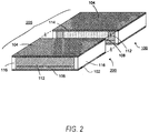
- phase shifter 100 can be seamlessly integrated with a standard substrate integrated waveguide (SIW) 200 , as illustrated in Figure 2 .
- SIW standard substrate integrated waveguide
- electrode 108 is situated below LC layer 114 and does not extend beyond the compartment in which LC layer is situated. In other words, in such an embodiment, electrode 108 only exists within the footprint of LC layer 114. As explained above, in other embodiments, electrode 108 can extend beyond the footprint of LC layer 114.
- the SIW portion 200 and the phase shifter portion 100 are fabricated together seamlessly as an integrated structure 205.
- electrode 108 can take on a variety of different forms. Two different embodiments, each having a different structure for the electrode, will be discussed in relation to Figures 3 to 6 .
- FIG. 3 illustrates a perspective view of LC layer 114 and electrode 108a of phase shifter 100 , according to an embodiment.
- the electrode 108a is a conductive layer having the same shape as the footprint of LC layer 114.
- electrode 108a has a planar surface corresponding to the footprint of LC layer 114.
- FIG. 4 illustrates graphs showing the simulated S (Scattering) parameters with different values of relative permittivity (from 2.5 to 3.5, in 0.2 steps) of LC layer 114 for the embodiment of Figure 3 .
- Graph 402 is a plot of the S21 parameter
- graph 404 is a plot of the S11 parameter.
- the S11 parameter represents the ratio between the microwave power coming out of port one and the microwave power injected into port one; the S21 parameter represents the ratio between the microwave power absorbed by the matched load to the microwave power injected into port one.
- the two parameters when the two parameters are expressed in dB format, it may be advantageous to have S11 as small as possible and S21 as close to zero as possible.
- the thickness of the phase shifter is 18.5 mm
- the thickness t a of dielectric layer 106 is 5 mil
- the thickness t b of dielectric layer 112 is 20 mil
- the width w c of LC layer 114 is 1.5 mm
- the width of the dielectric section W is 1.95 mm
- the thickness of each of ground plane 102 , ground plane 104 , and electrode 108a is 5 ⁇ m. From the graphs of Figure 4 , one can see that several transmission defects appear at different frequencies for different values of relative permittivity, represented as notches on the S21 curve and peaks on the S11 curve.
- This phenomenon is caused by the difference between the permittivity of LC layer 114 and the permittivity of dielectric layer 106 , as well as the shape of the electrode 108a. Due to the presence of the electrode 108a within the structure, two modes of microwave signal could exist below and above the electrode respectively at the same time. Furthermore, if the permittivity of the LC layer 114 and that of the dielectric layer 106 are different, the phase velocity of the two modes could be different. When the two modes pass through the phase shifter, they could be out of phase, which can attenuate the transmission and enhance the reflection at some frequencies.
- Figure 5A illustrates a perspective view of LC layer 114 and electrode 108b of phase shifter 100 , according to another embodiment.
- Figure 5B illustrates a perspective view of electrode 108b of Figure 5A on its own.
- the configuration of electrode 108b can help to reduce or eliminate the transmission defects discussed in relation to Figures 3 and 4 .
- electrode 108b is shaped like a grating having a plurality of electrode sections 501 that are spaced apart by gaps 502.
- the gaps 502 between electrode sections 501 do not extend all the way through the electrode such that each electrode section 501 is connected to a neighboring electrode section 501 by links 504.
- the gaps 502 are symmetrical and links 504 are positioned at the center of the lengths of each of the electrode sections 501 of electrode 108b .
- links 504 may be positioned elsewhere than at the center of the lengths of electrode sections 501.
- electrode 108b can also be considered to be comprised of separate electrodes that are coupled by links 504 where the links 504 are made of the same material as the electrodes.
- electrode sections 501 are substantially identically shaped. In some embodiments, electrode sections 501 have a rectangular shape. In some embodiments, the links 504 are made as thin as possible such that gaps 502 almost extend all the way through between the electrode sections 501. In an embodiment, electrode 108b can be said to comprise a series of equally spaced rectangular electrode ribs, the electrode ribs corresponding to electrode sections 501 , which are linked at the center of their lengths by links 504. In various embodiments, electrode sections 501 are only linked at the center and there are no links or connections at the extremities of the electrode sections 501.
- the structure of electrode 108b does not permit a parasitic mode of signal with a different phase velocity to be supported below electrode 108b .
- the two modes that are supported by electrode 108a in Figure 3 merge with each other if the gaps 502 are present in the electrode structure as shown with electrode 108b .
- Figure 6 illustrates graphs showing the simulated S (Scattering) parameters with different values of relative permittivity (from 2.5 to 3.5, in 0.2 steps) of LC layer 114 for an embodiment of a phase shifter incorporating the electrode of Figures 5A and 5B .
- Graph 602 is a plot of the S21 parameter
- graph 604 is a plot of the S11 parameter.
- the dimensions of the phase shifter are the same as those discussed above in relation to Figure 4 , except that the electrode is different.
- the graphs of Figure 6 show that transmission defects have been mitigated as compared to the embodiment of Figures 3 and 4 .
- electrode 108b as shown in Figures 5A and 5B may be selected for its performance.
- the period P of the electrode 108b is selected to be much less than the guided wavelength in order to minimize the occurrence of transmission defects.
- the period P of the electrode 108b is selected to be less than a quarter of the guided wavelength at the highest operating frequency, which are the dimensions used in the simulation corresponding to Figure 6 .
- the period ( P ) of electrode 108b refers to the width ( p1 ) of one electrode section 501 plus the length ( p2 ) of a link 504 (see Figure 5B ), where the width of the electrode section 501 and the length of the link 504 are in the same direction.
- electrode 108b is comprised of repetitive elements (e.g. the electrode sections 501 and links 504 ) and the period refers to period of repetition.
- p2 is selected to be as small as the fabrication process allows for and p1 is selected to be as large as possible without creating a transmission defect. This will result in a maximum possible electrode area for electrode 108b , which allows for a substantially uniform static electric field distribution.
- phase shifter 100 can be fabricated using multi-layer printed circuit board (PCB) fabrication techniques.
- the basic material for such fabrication is a PCB laminate having one dielectric layer and two copper layers which are attached on each side of the dielectric layer.
- the basic fabrication process includes copper etching, via (hole) cutting, via (hole) metallization and so forth as will be explained in greater detail below.
- conductive sidewalls 116 are generated by via cutting and metallization.
- an additional substrate layer is used above the top ground plane 104 to allow for the formation of an electric short (metallization) through ground plane 102 , sidewalls 116 and ground plane 104.
- the additional substrate layer and the top ground plane 104 are provided by a PCB laminate.
- Method 700 may contain additional or fewer processes than shown and/or described, and may be performed in a different order.
- a first metal layer is provided.
- this metal layer corresponds to ground plane 102.
- a first dielectric layer is provided.
- this dielectric layer corresponds to dielectric 106.
- an electrode which in an embodiment corresponds to electrode 108 , is created on the surface of first dielectric layer that is opposite the first metal layer.
- this dielectric layer corresponds to dielectric 112.
- a compartment is created to hold LC layer 114.
- the compartment can comprise a grove or cavity that is carved in the second dielectric.
- a hole can be cut through the second dielectric and the compartment is formed once the second dielectric layer is attached to the first dielectric layer.
- the second dielectric layer is attached to the first dielectric layer.
- the dielectric layers are attached to one another by chemically bonding them together.
- epoxy is used to bond the dielectric layers together.
- the dielectric layers are bonded together by other methods other than the use of chemical bonding agents.
- the walls of the compartment are coated with appropriate alignment chemicals as discussed above in order to achieve a consistent orientation of LC molecules in LC layer 114 , for example in a direction perpendicular to the electric field of a microwave signal passing through the LC layer 114. In an embodiment, this corresponds to LC molecules being oriented parallel to the plane of electrode 108.
- the compartment is filed with liquid crystal.
- a top metal layer is provided over the second dielectric.
- the top metal layer corresponds to top ground plane 104.
- a surface of the top metal layer for example, the surface that will be in contact with LC layer 114 , is coated with alignment chemicals.
- vias are created through the top metal layer as well as the first and second dielectric layers.
- the vias are metallized.
- the metallized vias correspond to sidewalls 116.
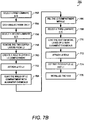
- Figure 7B is a flow chart diagram illustrating a method of fabrication in accordance with an embodiment of the present disclosure.
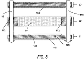
- Figure 8 is a schematic diagram illustrating a representation of how the various layers are combined during the fabrication method of Figure 7B .
- Method 750 illustrated in Figure 7B relates to a fabrication method using multi-layer printed circuit board (PCB) fabrication techniques.
- Method 750 may contain additional or fewer processes than shown and/or described, and may be performed in a different order.
- a first laminate (L1) is selected.
- the first laminate L1 includes one dielectric layer and two copper layers.
- other metals other than copper may be used.
- electrode 108 is created on L1 by etching one of the copper layers.
- a second laminate (L2) is selected.
- a hole having the shape of the LC layer's footprint, is created in L2.
- the hole may be created by cutting through L2. Accordingly, this generates a compartment or container for the LC once L2 is attached to L1.
- L2 is attached to L1.
- L2 is chemically bonded to L1.
- L2 is bonded to L1 with epoxy.
- the hole in L2 corresponding to the LC compartment is aligned with electrode 108.
- electrode 108 extends beyond the dimensions of the hole and the hole is not carefully aligned with electrode 108.
- the inner walls of the LC compartment are coated with alignment chemicals.
- both walls of the dielectric layer 112 and the surface of the electrode 108 are coated with alignment chemicals.
- the surfaces of dielectric layer 112 and electrode 108 are coated with appropriate alignment chemicals as discussed above in order to achieve orientations of LC molecules in LC layer 114 , that are generally perpendicular to the direction of the electric field of a signal propagating through LC layer 114. In an embodiment, this corresponds to molecule orientations that are parallel to the plane of electrode 108.
- alignment chemicals are described above.
- the LC compartment is filled with LC.
- a third laminate (L3) is selected.
- a surface of the bottom copper layer of L3, which corresponds to ground plane 104 is coated with alignment chemicals.
- L3 is attached to L2. Therefore, L3 covers the LC compartment.
- L3 is chemically bonded to L2.
- L3 is bonded to L2 with epoxy.
- the bottom copper layer of L3 provides ground plane 104.
- vias are cut through L3, L2, and L1.
- the vias are metallized and this forms the sidewalls 116.
- the metal sidewalls provide an electrical short between the top ground plane 104 and bottom ground plane 102.
- the structure produced by the fabrication method of Figure 7B can include not only one or more phase shifters but also one or more waveguide sections that are integrated with the phase shifter(s).
- the electrode, hole, and LC would be created only in the portion of the structure where the phase shifter is located, and the remaining portion of the structure would correspond to a substrate integrated waveguide similar to the structure illustrated in Figure 2 .
- electrode 108 is not in contact with LC layer 114.
- a groove or a well is cut in dielectric 112 to form the compartment for LC layer 114.
- some fabrication processes may not support creating the groove or well in the dielectric.
- the depth of the LC compartment and therefore the thickness of LC layer 114 is reduced, which in turn may reduce the tuning range of phase shifter.
- Figure 9 is a flow chart diagram illustrating a method 900 of fabrication in accordance with an embodiment of the present disclosure.
- Figure 10A is a schematic diagram illustrating a representation of how the various layers are combined during the fabrication method of Figure 9 .
- Figure 10B illustrates an embodiment of a phase shifter 100b that is produced as a result of the method 900 illustrated in Figure 9 , with the substrate and top copper layer of L3 omitted for clarity.
- Method 900 illustrated in Figure 9 relates to a fabrication method using multi-layer printed circuit board (PCB) fabrication techniques.
- Method 900 may contain additional or fewer processes than shown and/or described, and may be performed in a different order.
- a first laminate is selected.
- the laminate is with one dielectric layer and two copper layers.
- metals other than copper may be used.
- electrode 108 is created on L1A by etching one of the copper layers.
- a second laminate (L2A) is selected.
- one of the copper layers is removed from L2A.
- a hole having the shape of the LC layer's footprint, is created in L2A.
- the hole may be created by cutting though L2A. Accordingly, this generates a compartment or container for the LC once L2A is attached to L1A.
- L2A is attached to L1A with the non-copper-surface of L2A being placed against L1A.
- L2A is chemically bonded to L1A.
- L2A is bonded to L1A with epoxy.
- the hole in L2 corresponding to the LC compartment is aligned with electrode 108.
- electrode 108 extends beyond the dimensions of the hole and the hole is not carefully aligned with electrode 108.
- the inner walls of LC compartment are coated with alignment chemicals.
- both walls of the dielectric layer 112 and the surface of the electrode 108 are coated with the alignment chemicals.
- the surfaces of dielectric layer 112 and electrode 108 are coated with different alignment chemicals in order to achieve orientations of LC molecules in LC layer 114 , that are generally perpendicular to the direction of the electric field of a signal propagating through LC layer 114.In an embodiment, this corresponds to molecule orientations that are parallel to the plane of electrode 108.
- alignment chemicals are described above.
- vias are cut through L2A and L1A.
- the vias are metallized and this forms the sidewalls 116.
- the LC compartment is filled with LC.
- the LC compartment is filled after the vias have been metallized.
- a third laminate (L3A) is selected.
- a surface of the bottom copper layer of L3A, which corresponds to ground plane 104b, is coated with alignment chemicals.
- L3A is attached to L2A.
- L3A is chemically bonded to L2A.
- L3A is bonded to L2A with epoxy.
- the dielectric layers are bonded together by methods other than the use of chemical bonding agents.
- the bottom copper layer of L3A provides ground plane 104b .
- the portion of the bottom metal layer of L3A overlying the LC compartment is not covered with epoxy. In some embodiments, this is accomplished by utilizing suitable masks during the fabrication process.
- FIG 10B illustrates an embodiment, of a phase shifter 100b that is produced as a result of the method 900 illustrated in Figure 9 .
- the vias are cut through only L2A and L1A, ground plane 104b of phase shifter 100b is not shorted to side walls 116 and ground plane 102. Accordingly, in phase shifter 100b only two laminates are dedicated to the phase shifter.
- the bottom copper of L3A is used as a shielding cover and the top copper and the dielectric substrate of L3A can be used to support other circuits in, for example, an integrated multilayer system.
- phase shifter portion corresponds to the part of the structure where the LC compartment is situated and the waveguide portion corresponds to the portion where the LC compartment is absent.
- non-conductive epoxy is utilized.
- a conductive bonding agent such as a conductive epoxy is utilized.
- Epoxy layer 970 separates ground plane 104b from the top metal layer 980 of L2A and therefore from sidewalls 116. The impact of this epoxy gap between ground plain 104b and sidewalls 116 , when the epoxy is a non-conductive epoxy, is discussed below in relation to Figure 11 .
- phase shifter portion of the structure produced by method 900 of Figure 9 is not a waveguide in the conventional sense. However, if the epoxy gap is small enough, the phase shifter portion of the structure produced by method 900 of Figure 9 supports the same mode of microwave signals.
- the waveguide portion produced by method 900 will be a true waveguide as the top metal layer 980 of L2A is electrically coupled to the side walls and extends over the dielectric in the waveguide portion of the apparatus.
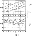
- Figure 11 illustrates graphs 1102 and 1104 showing the simulated S parameters for phase shifter 100b of Figure 10B , when non-conductive bonding material is used to bond L3A to L2A. Accordingly, Figure 11 allows one to examine the impact of the epoxy layer 970 through simulation.
- the dimensions of the phase shifter, including the electrode, used in the simulation corresponding to Figure 11 are the same as the dimensions used for the simulation of Figure 6 . From comparing Figures 11 and 6 , it can be seen that in Figure 11 , the S21 parameter has decreased by less than 1dB and the S11 parameters are still mostly less than -20dB.
- the transmission performance in Figure 11 is well maintained as compared to Figure 6 .
- Figure 12 illustrates a top cross-sectional view of a phase shifter, in accordance with an embodiment of the present disclosure.
- the view in Figure 12 illustrates the connection of a DC bias line 1202 to electrode 108b .
- Bias line 1202 is extended from the electrode 108b through the sidewall opening 1204 to the outside of the phase shifter and connected to a bias voltage source, for example, the positive terminal of the DC bias.
- the vias on either side of the phase shifter are not continuous but are cut in sections that are spaced apart from each other.
- the sidewalls 116 are not continuous along the length of the phase shifter and a dielectric can fill the space of sidewall opening 1204 , which is the space between side walls 116.
- the bias line is created by etching it together with the electrode and the bias line is positioned so as to be aligned with one of the spaces between the vias.
- the bias line extends out of the phase shifter between dielectrics 106 and 112.
- the negative terminal of the DC bias is coupled to the top ground plane 104.
- sidewall opening 1204 is made to be smaller than 1/10 of the free space wavelength of the microwave signal propagating in the phase shifter, such that the radiation loss from the gap is negligible.
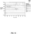
- Figure 13 illustrates a graph 1302 showing the phase tuning performance of the phase shifter 100b of Figure 10B .
- the dimensions are the same as those used in Figures 4 and 6 .
- the phase can be tuned between 0° and 415° with the relative permittivity of LC changed from 2.5 to 3.5.
- the curve corresponding to relative permittivity of 3.5 exhibits the least flat of the curves of Figure 13 and, across the range of frequencies, it exhibits a maximum deviation of phase of 9°.
- the phase shift of each of the curves is with respect to the phase at relative permittivity of 2.5 at each frequency.
Landscapes
- Engineering & Computer Science (AREA)
- Chemical & Material Sciences (AREA)
- Ceramic Engineering (AREA)
- Manufacturing & Machinery (AREA)
- Materials Engineering (AREA)
- Structural Engineering (AREA)
- Organic Chemistry (AREA)
- Variable-Direction Aerials And Aerial Arrays (AREA)
- Waveguides (AREA)
- Waveguide Switches, Polarizers, And Phase Shifters (AREA)
- Laminated Bodies (AREA)
Description
- The present disclosure relates generally to phase shifters.
- Phase shifters are used in microwave systems such as phased array systems. Phase shifters are used to provide a controllable phase shift of a microwave signal and can be constructed using various technologies. Some commercially available phase shifters include active components such as transistors and diodes and may be based on micro-electromechanical systems (MEMS). Phase shifters can be used in a variety of technology areas such as, for example, telecommunications and radar systems.
- For example,
US 2012/0194399A1 refers to surface scattering antennas providing adjustable radiation fields by adjustably coupling scattering elements along a wave-propagating structure. In some approaches, the scattering elements are complementary metamaterial elements. In some approaches, the scattering elements are made adjustable by disposing an electrically adjustable material, such as a liquid crystal, in proximity to the scattering elements. Methods and systems provide control and adjustment of surface scattering antennas for various applications. - Further, INGO WOLFF: "Integrated beam steerable antennas in LTCC-technology", 1 March 2010 refers to two concepts of building highly integrated beam steerable antennas for space applications: As a first example, an integrated phased array antenna using liquid crystal phase shifters in a LTCC technology shows promising results for application in space communication. As a second example, a fully integrated digital beam steering antenna in LTCC technology demonstrates how a high integration factor for an antenna system including active microwave circuits and a cooling system can be realized.
- Further, FRANKE TOBIAS ET AL: "Tunable Ka-band waveguide resonators and a small band band-pass filter based on liquid crystals", 6. October 2014 refers to a design of Liquid Crystal filled waveguide resonators.
- Improvements in phase shifters are desirable. For example, it is generally desirable for phase shifters to have relatively low power requirements, exhibit relatively low losses during operation, and have relatively low fabrication costs.
- In a first aspect, the present disclosure provides an apparatus according to claim 1.
- The liquid crystal (LC) layer fills the space of the compartment. A bias line is coupled to the electrode.
- The electrode may form at least a portion of a surface of the compartment.
- The apparatus may further include a waveguide portion and a phase shifter portion. The waveguide portion corresponds to the portion of the apparatus where the dielectric fills the entire volume between the conductive walls. The phase shifter portion corresponds to the portion of the apparatus that includes the compartment.
- The apparatus may further include an opening in one of the conductive walls and the bias line passes through the opening.
- The housing may be shaped as a rectangular prism.
- At least one alignment chemical coating may be applied on at least one surface of the compartment. The at least one alignment chemical coating may be selected to, in the absence of an applied static electric field, align molecules in an orientation that is parallel to a plane of the electrode.
- In another aspect, a method of fabricating a microwave apparatus is defined by
claim 8. - Providing the bottom metal layer and providing the first dielectric may comprise providing a first laminate layer, where the first laminate layer is a printed circuit board laminate that has a substrate layer, a top metal layer, and a bottom metal layer. Providing the electrode may include etching the top metal layer of the first layer to form the electrode.
- Providing the second dielectric layer may include providing a second laminate layer and removing the top and bottom metal layers from the second laminate.
- Creating the compartment may include creating a hole in the second dielectric and attaching the second dielectric to the first dielectric.
- The method may further include applying at least one alignment chemical coating to at least one surface of the apparatus in contact with the LC layer. The at least one alignment chemical coating may be selected to, in the absence of an applied static electric field, align molecules of the LC layer in an orientation that is parallel to a plane of the electrode.
- The electrode may comprise a plurality of sections where each of the sections are spaced apart from adjacent sections. The electrode may further include links that electrically connect each of the plurality of sections to an adjacent section.
- The method may include creating at least two vias on one side of the apparatus, where the at least two vias have a space therebetween. The method may also include generating a bias line that is coupled to the electrode and that extends through the space between the vias.
- Providing the second dielectric layer may include providing a second laminate layer and removing the bottom metal layer from the second laminate. Creating the compartment may also include creating a hole through the top metal layer of the second laminate. The method may further include providing a third laminate layer and attaching the third laminate to the second laminate. In some embodiments, metallizing the vias may be performed before the compartment is filled with a liquid crystal layer.
- Other aspects and features of the present disclosure will become apparent to those ordinarily skilled in the art upon review of the following description of specific embodiments in conjunction with the accompanying figures.
- Embodiments of the present disclosure will now be described, by way of example only, with reference to the attached Figures.
-
Figure 1A is a perspective view of an example phase shifter, in accordance with an embodiment of the present disclosure; -
Figure 1B illustrates a perspective view of the dielectric layer ofFigure 1A in a first state, in accordance with an embodiment of the present disclosure; -
Figure 1C illustrates a perspective view of the dielectric layer ofFigure 1A in a second state, in accordance with an embodiment of the present disclosure; -
Figures 1D and 1E illustrate alternative shapes for an LC compartment, in accordance with embodiments of the present disclosure; -
Figure 2 is a perspective view of an example phase shifter integrated with a substrate integrated waveguide, in accordance with an embodiment of the present disclosure; -
Figure 3 is a perspective view of the liquid crystal layer and an example electrode of the phase shifter ofFigure 1A , in accordance with an embodiment of the present disclosure; -
Figure 4 illustrates graphs showing scattering parameters of a phase shifter incorporating the electrode ofFigure 3 ; -
Figure 5A is a perspective view of the liquid crystal layer and another example electrode of the phase shifter ofFigure 1A , in accordance with another embodiment of the present disclosure; -
Figure 5B is a perspective view of the electrode ofFigure 5A ; -
Figure 6 illustrates graphs showing scattering parameters of a phase shifter incorporating the electrode ofFigures 5A and 5B ; -
Figure 7A is a flowchart diagram illustrating an example process of fabricating a phase shifter, in accordance with an embodiment of the present disclosure; -
Figure 7B is a flowchart diagram illustrating an example process of fabricating a phase shifter, in accordance with an embodiment of the present disclosure; -
Figure 8 is a schematic diagram illustrating an example of the order in which various layers are combined in the process ofFigure 7B , in accordance with an embodiment of the present disclosure; -
Figure 9 is a flowchart diagram illustrating an example process of fabricating a phase shifter, in accordance with another embodiment of the present disclosure; -
Figure 10A is a schematic diagram illustrating an example of the order in which various layers are combined in the process ofFigure 9 , in accordance with an embodiment of the present disclosure; -
Figure 10B is a perspective view of an example phase shifter constructed in accordance with the process ofFigure 9 , with some layers omitted for clarity; -
Figure 11 illustrates graphs showing scattering parameters of a phase shifter ofFigure 10 , incorporating the electrode ofFigure 5 ; -
Figure 12 is a top cross-sectional view of an example phase shifter, in accordance with an embodiment of the present disclosure; and -
Figure 13 illustrates a graph showing the phase tuning performance of the example phase shifter ofFigure 10B . - Various embodiments disclosed herein relate to variable microwave phase shifters that incorporate a liquid crystal layer. The term "microwave", as used herein, refers to an electromagnetic wave that includes, but is not limited to, a frequency component in the range of 1 kHz to 1000 GHz. Various embodiments of the phase shifters described herein may be incorporated with a substrate integrated waveguide.
- Reference is first made to
Figure 1A , which illustrates a perspective view of avariable phase shifter 100, in accordance with an embodiment of the present disclosure.Phase shifter 100 includes a variety of components which will now be briefly described.Bottom ground plane 102 andtop ground plane 104 are conductive layers. Accordingly, in an embodiment,bottom ground plane 102 andtop ground plane 104 correspond to top and bottom metal layers ofphase shifter 100. In various embodiments, suitable materials forground planes - In an embodiment,
dielectric layer 106 comprises a supporting substrate. In various embodiments,dielectric layer 106 can comprise any suitable dielectric material, which can include, but is not limited to, polytetrafluoroethylene (PTFE), ceramic, glass, SiO2, appropriately-doped or undoped GaAs, and combinations thereof. -
Electrode 108 is a conductive layer and in various embodiments can comprise, but is not limited to, copper, gold, silver, and alloys thereof. In an embodiment,electrode 108 spans an inside surface of dielectric 106 between either side ofdielectric 112. In some embodiments,electrode 108 is larger and can extend beyond the walls ofdielectric 112. In some embodiments,electrode 108 extends betweendielectrics dielectric layer 112 can comprise any suitable material, which can include, but is not limited to, polytetrafluoroethylene (PTFE), ceramic, glass, SiO2, GaAs and combinations thereof. In some embodiments,dielectrics dielectrics Dielectrics dielectric layers dielectrics dielectrics dielectrics dielectrics -
Dielectrics top ground plane 104, define a compartment or container. LC (Liquid Crystal)layer 114 fills the space of the compartment. In various embodiments,electrode 108 is aligned with the compartment. In some embodiments, this is achieved by having at least a portion of the electrode span an entire surface the compartment. In some embodiments,electrode 108 forms an inside surface of the compartment. In other embodiments,electrode 108 is situated on an inside surface of the compartment. In yet other embodiments,electrode 108 is outside of the compartment and is not in physical contact withLC layer 114. In various embodiments,LC layer 114 can comprise, but is not limited to, twisted nematic LCs, super-twisted nematic LCs and chiral nematic LCs. The nematic phase is one of the most common phases of liquid crystals and is generally used for tunable electronic devices because the phase generally has attractive properties, such as large tuning ranges and low losses. However, it should be understood that while some embodiments disclosed herein utilize nematic LCs, other embodiments can also utilize other phases of LCs. Accordingly, various embodiments herein utilize single liquid crystal compounds or liquid crystal mixtures that comprises two or more single liquid crystal compounds. In yet other embodiments, other liquid crystal compounds can also be utilized. - In an embodiment, sidewalls 116 each span between
ground plane Sidewalls 116 are comprised of a conductive material, which can be the same as the material used forground planes sidewalls 116 include, but are not limited to, copper, gold, silver, and alloys thereof. In an embodiment, sidewalls 116 need not be continuous along the length ofphase shifter 100. For example, in some such embodiments, sidewalls 116 may comprise sections of conductive material that appear in a repetitive pattern along the length of the phase shifter. In some such embodiments, the spaces between the sections ofsidewalls 116 may be filled with a dielectric, such asdielectric - Although not illustrated in
Figure 1A ,phase shifter 100 also includes a bias line coupled toelectrode 108, which allows for a bias voltage to be applied toelectrode 108. The bias line is discussed in greater detail below in relation toFigure 12 . - As can be seen from
Figure 1A , in an embodiment,phase shifter 100 can be considered to include a housing. The housing includes four conductive walls, which correspond totop ground plane 104,bottom ground plane 102, and sidewalls 116. Each conductive wall is opposite another one of the conductive walls. In an embodiment, the phase shifter is shaped like a rectangular prism with each metal wall corresponding to one of four faces of the rectangular prism. - In an embodiment,
LC layer 114 includes molecules that are anisotropic and can be represented by vectors. When certain conditions are applied to a LC bulk, the majority of molecules of the LC bulk will take on the same orientation. In an embodiment, the LC molecules generally have a rod-like shape and the orientation refers to the longitudinal direction of the rod shape. When the majority of molecules of the LC bulk are oriented in the same direction, the lowest permittivity εlow can be found in a direction perpendicular to the vector representing the molecules and the highest permittivity ε high can be found in the direction parallel to the vector. - In certain embodiments, the inner surfaces of
dielectric 112, the top side ofelectrode 108 and the bottom side of 104 that are in contact with theLC layer 114 may be coated with thin layers of chemicals for the alignment of the LC molecules withinLC layer 114. These chemicals will be referred to herein as alignment chemicals. In an embodiment, the alignment chemicals can include, but are not limited to, polyimides. Due to the surface anchoring effect, some alignment chemicals will orient the vector of the LC molecules in a direction that is parallel to the coated surface, while some other chemicals will orient the vector of the LC molecules in a direction that is perpendicular to the surface. In various embodiments, such surface treatments or coatings can be used to achieve particular initial permittivity values of the LC bulk that makes upLC layer 114. - In various embodiments of the phase shifters disclosed herein, when no bias voltage is applied between
electrode 108 andground plane 104, the LC molecules ofLC layer 114 are in an initial state in which a substantial portion of the molecules are generally oriented in directions that are perpendicular an electric field of a signal passing throughLC layer 114. In an embodiment, this corresponds to the molecules having orientations that are parallel to the plane ofelectrode 108. In some such embodiments, surface coatings, which may include alignment chemicals, are applied to the top surface ofelectrode 108 and the bottom side of ground plane 104 (i.e. the surfaces ofelectrode 108 and ofground plane 104 that are in contact with the LC layer) in order to orient the vector of the LC molecules inLC layer 114 in directions that are parallel to the coated surface and perpendicular to the electric field of a microwave signal passing thoughLC layer 114. In such embodiments, due to the surface anchoring effect as well the surface coatings, in the initial state (i.e. without a bias applied to the electrode), the LC molecules have nearly the same orientation along the surface of theelectrode 108 andtop ground plane 104. In addition, in such embodiments, the inner surfaces of dielectric 112 can be coated with alignment chemicals that orient the vector of the LC molecules inLC layer 114 in directions that are perpendicular to both the coated surface and the electric field of a microwave signal passing thoughLC layer 114. Consequently, when such embodiments ofphase shifter 100 are in use, such as when it is coupled to or integrated with a waveguide, and a microwave signal is propagated into it while no bias is applied to the electrode, the transverse electric (TE) mode with the lowest cutoff frequency (TE10 mode) of the microwave signal passing through theLC layer 114 encounters aLC layer 114 having molecule orientations that are mostly perpendicular to the field direction. This results in an effective permittivity of theLC layer 114 that is close to ε low . -
Figure 1B is a perspective view ofLC layer 114 ofphase shifter 100, in a first state, which corresponds to an absence of a static electric field. In other words,Figure 1B corresponds to the situation where no bias voltage is applied toelectrode 108. The remaining elements ofphase shifter 100 are omitted fromFigure 1B for clarity. As can be seen, when suitable coating chemicals are utilized, theLC molecules 150 can have various orientations. However, they are generally oriented in directions that are perpendicular to theelectric field 152 of a microwave signal passing through theLC layer 114. In an embodiment, this corresponds toLC molecules 150 being oriented parallel to the plane ofelectrode 108.Electric field 152 ofFigure 1B illustrates the TE10 mode of a microwave signals. - When a bias voltage of a sufficiently high value is applied between
electrode 108 andground plane 104, then the majority of the LC molecules ofLC layer 114 are rotated along the direction of the static electric field established by the bias voltage. Accordingly, under such bias conditions, the TE10 mode of the microwave signal passing throughLC layer 114 encounters a LC bulk having molecule orientations that are mostly aligned with the electric field of the TE10 mode and therefore the effective permittivity ofLC layer 114 is close to ε high . With other intermediate bias voltages, the effective permittivity is between the two values (ε low and ε high ) and increases as the bias voltage is increased. -
Figure 1C is a perspective view ofLC layer 114 ofphase shifter 100, in a second state, which corresponds to the presence of a static electric field. In other words,Figure 1C corresponds to the situation where a bias voltage is applied toelectrode 108.Arrow 154 represents the direction of the static electric field. The remaining elements ofphase shifter 100 are omitted fromFigure 1C for clarity. As can be seen, when a static electric field is applied betweenelectrode 108 andtop ground plane 104,LC molecules 150 take on an orientation that is the direction of static electric field. Accordingly, under such conditions,molecules 150 are generally aligned with theelectric field 152 of the microwave signal.. - Although the compartment that holds
LC layer 114 is shown has having a shape generally corresponding to a rectangular prism, other shapes may be used.Figure 1D illustrates analternative shape 160a for the LC compartment.Figure 1E illustrates anotheralternative shape 160b for the LC compartment. These are examples only. Other embodiments may use other shapes for the LC compartment. - In contrast to the static electric field corresponding to the bias voltage applied between
electrode 108 andground plane 104, the electric field of the microwave signal does not impact the orientation of the LC molecules ofLC layer 114 because the direction of the electric field of the microwave signal changes too quickly for the LC molecules to follow. - As mentioned above, with the use of suitable surface coatings, the surface anchoring effect establishes a low initial permittivity state of
LC layer 114. In some embodiments, this can be used to achieve a larger phase tuning range ofphase shifter 100 than would be otherwise achieved without the coating. Examples of coating chemicals that will orient the vector of LC molecules in a direction that is parallel to the coated surface include, but are not limited, to SE-150 and SE-3310 from Nissan Chemical Industries, Japan as well as AL3046 and AL23201 from JSR Corporation, Japan. Examples of coating chemicals that will orient the vector of LC molecules in a direction that is perpendicular to the coated surface include, but are not limited to, SE-1211 and SE-5300 from Nissan Chemical Industries, Japan as well as AL63702 from JSR Corporation, Japan. - Examples of commercial LC materials or LC mixtures that can be used for
LC layer 114 in various embodiments include, but are not limited to E7, E44, E48, E31, E63, E80, and BL003, BL006, BL033, BL037, BL048, BL087, BL101, BL112, BL126, and ZLI-3308, ZLI-3273, ZLI-4801, ZLI-4692, ZLI-5048-000, ZLI-5049-100, ZLI-5081, ZLI-5100-100, ZLI-5800-000, and TL202, TL203, TL204, TL205, and MLC-6267, MLC-6284, MLC-6287, MLC-6288, MLC-6406, MLC-6422, MLC-6423, MLC-6425, MLC-6435, MLC-6437, MLC-7700, MLC-7800, MLC-9000, MLC-9100, MLC-9200, MLC-9300, MLC-10000, and GT3-23001, GT3-24002, GT3-24004, GT3-25003, and TUD-224, TUD-424, TUD-325, and MLC-6041-100, MDA-00-350, K15. In addition, some embodiments utilize new LC mixtures, such as for example, New Mix A, B and C from Merck, Germany, which are disclosed in Manabe, Atsutaka. "Liquid crystals for microwave applications." SPIE OPTO. International Society for Optics and Photonics, 2013. - For mass production of some embodiments of the phase shifters disclosed herein, standard printed circuit substrate materials can be utilized for
dielectrics dielectrics dielectrics - In some embodiments, the permittivity tuning range of
LC layer 114 is considered when selecting the substrate materials fordielectrics LC layer 114 anddielectric layers - In some embodiments, the TE10 mode is the only mode permitted to propagate in the phase shifter. On the other hand, as a rule of thumb, the accepted limits of the operation frequency of a waveguide are between 125% and 189% of the lower cutoff frequency, in an embodiment. Accordingly, in an embodiment, the width of the dielectric section W is selected to satisfy the rule throughout the permittivity tuning range from εlow to εhigh . Therefore, in such embodiments, W is selected so that the conditions



dielectric 112 has a lower limit. Therefore, in some embodiments, in order to have the maximum LC filling rate (i.e. the largest possible LC layer and in turn a maximum phase tuning range), W is chosen to be close to but no more than
- In addition, in such an embodiment, the total thickness T of
dielectric layers dielectric layers dielectric layers dielectric layers dielectric layer 106 is selected to be as thin as possible while maintaining sufficient mechanical strength. Then, the thickness tb ofdielectric layer 112 is selected to provide the desired trade-off between a larger phase tuning range and a lower maximum tuning voltage. - In an embodiment,
phase shifter 100 can be seamlessly integrated with a standard substrate integrated waveguide (SIW) 200, as illustrated inFigure 2 . In an embodiment,electrode 108 is situated belowLC layer 114 and does not extend beyond the compartment in which LC layer is situated. In other words, in such an embodiment,electrode 108 only exists within the footprint ofLC layer 114. As explained above, in other embodiments,electrode 108 can extend beyond the footprint ofLC layer 114. In some embodiments, during circuit fabrication, theSIW portion 200 and thephase shifter portion 100 are fabricated together seamlessly as anintegrated structure 205. - In various embodiments of
phase shifter 100,electrode 108 can take on a variety of different forms. Two different embodiments, each having a different structure for the electrode, will be discussed in relation toFigures 3 to 6 . - Reference is first made to
Figure 3 , which illustrates a perspective view ofLC layer 114 andelectrode 108a ofphase shifter 100, according to an embodiment. For purposes of clarity, the other parts ofphase shifter 100 are omitted fromFigure 3 . These other parts can be the same as described above and illustrated inFigure 1A . In this embodiment, theelectrode 108a is a conductive layer having the same shape as the footprint ofLC layer 114. In other words, in an embodiment,electrode 108a has a planar surface corresponding to the footprint ofLC layer 114. - Reference is now made to
Figure 4 , which illustrates graphs showing the simulated S (Scattering) parameters with different values of relative permittivity (from 2.5 to 3.5, in 0.2 steps) ofLC layer 114 for the embodiment ofFigure 3 .Graph 402 is a plot of the S21 parameter andgraph 404 is a plot of the S11 parameter. Given that various embodiments ofphase shifter 100 may be operated as a two port reciprocal device, one can name the two ports as port one and port two arbitrarily. Then under the condition that port two is connected to a matched load and port one is connected to a microwave source, the S11 parameter represents the ratio between the microwave power coming out of port one and the microwave power injected into port one; the S21 parameter represents the ratio between the microwave power absorbed by the matched load to the microwave power injected into port one. In some embodiments, when the two parameters are expressed in dB format, it may be advantageous to have S11 as small as possible and S21 as close to zero as possible. - For the simulation corresponding to
Figure 4 , the following parameters were selected: length of the phase shifter is 18.5 mm, the thickness ta ofdielectric layer 106 is 5 mil, the thickness tb ofdielectric layer 112 is 20 mil, the width wc ofLC layer 114 is 1.5 mm, the width of the dielectric section W is 1.95 mm, and the thickness of each ofground plane 102,ground plane 104, andelectrode 108a is 5 µm. From the graphs ofFigure 4 , one can see that several transmission defects appear at different frequencies for different values of relative permittivity, represented as notches on the S21 curve and peaks on the S11 curve. This phenomenon is caused by the difference between the permittivity ofLC layer 114 and the permittivity ofdielectric layer 106, as well as the shape of theelectrode 108a. Due to the presence of theelectrode 108a within the structure, two modes of microwave signal could exist below and above the electrode respectively at the same time. Furthermore, if the permittivity of theLC layer 114 and that of thedielectric layer 106 are different, the phase velocity of the two modes could be different. When the two modes pass through the phase shifter, they could be out of phase, which can attenuate the transmission and enhance the reflection at some frequencies. - Reference is now made to
Figures 5A and 5B. Figure 5A illustrates a perspective view ofLC layer 114 andelectrode 108b ofphase shifter 100, according to another embodiment. For purposes of clarity, the other parts ofphase shifter 100 are omitted fromFigure 5A . For greater clarity,Figure 5B illustrates a perspective view ofelectrode 108b ofFigure 5A on its own. In some embodiments, the configuration ofelectrode 108b can help to reduce or eliminate the transmission defects discussed in relation toFigures 3 and4 . In the embodiment illustrated inFigures 5A and 5B ,electrode 108b is shaped like a grating having a plurality ofelectrode sections 501 that are spaced apart bygaps 502. In order to maintain an equipotential throughoutelectrode 108b, thegaps 502 betweenelectrode sections 501 do not extend all the way through the electrode such that eachelectrode section 501 is connected to a neighboringelectrode section 501 bylinks 504. In the embodiment illustrated inFigures 5A and 5B , thegaps 502 are symmetrical andlinks 504 are positioned at the center of the lengths of each of theelectrode sections 501 ofelectrode 108b. In other embodiments,links 504 may be positioned elsewhere than at the center of the lengths ofelectrode sections 501. In an embodiment,electrode 108b can also be considered to be comprised of separate electrodes that are coupled bylinks 504 where thelinks 504 are made of the same material as the electrodes. - In various embodiments,
electrode sections 501 are substantially identically shaped. In some embodiments,electrode sections 501 have a rectangular shape. In some embodiments, thelinks 504 are made as thin as possible such thatgaps 502 almost extend all the way through between theelectrode sections 501. In an embodiment,electrode 108b can be said to comprise a series of equally spaced rectangular electrode ribs, the electrode ribs corresponding to electrodesections 501, which are linked at the center of their lengths bylinks 504. In various embodiments,electrode sections 501 are only linked at the center and there are no links or connections at the extremities of theelectrode sections 501. - In various embodiments, the structure of
electrode 108b does not permit a parasitic mode of signal with a different phase velocity to be supported belowelectrode 108b. In other words, the two modes that are supported byelectrode 108a inFigure 3 merge with each other if thegaps 502 are present in the electrode structure as shown withelectrode 108b. - Reference is now made to
Figure 6 , which illustrates graphs showing the simulated S (Scattering) parameters with different values of relative permittivity (from 2.5 to 3.5, in 0.2 steps) ofLC layer 114 for an embodiment of a phase shifter incorporating the electrode ofFigures 5A and 5B .Graph 602 is a plot of the S21 parameter andgraph 604 is a plot of the S11 parameter. For the simulation corresponding to the graphs ofFigure 6 , the dimensions of the phase shifter are the same as those discussed above in relation toFigure 4 , except that the electrode is different. The graphs ofFigure 6 show that transmission defects have been mitigated as compared to the embodiment ofFigures 3 and4 . The reflection is less than -20dB and the insertion loss is less than 1dB. Accordingly, in various embodiments,electrode 108b as shown inFigures 5A and 5B may be selected for its performance. In various embodiments, the period P of theelectrode 108b is selected to be much less than the guided wavelength in order to minimize the occurrence of transmission defects. In some embodiments, the period P of theelectrode 108b is selected to be less than a quarter of the guided wavelength at the highest operating frequency, which are the dimensions used in the simulation corresponding toFigure 6 . - The period (P) of
electrode 108b refers to the width (p1) of oneelectrode section 501 plus the length (p2) of a link 504 (seeFigure 5B ), where the width of theelectrode section 501 and the length of thelink 504 are in the same direction. In some embodiments,electrode 108b is comprised of repetitive elements (e.g. theelectrode sections 501 and links 504) and the period refers to period of repetition. In some embodiments, p2 is selected to be as small as the fabrication process allows for and p1 is selected to be as large as possible without creating a transmission defect. This will result in a maximum possible electrode area forelectrode 108b, which allows for a substantially uniform static electric field distribution. - Various embodiments of
phase shifter 100 can be fabricated using multi-layer printed circuit board (PCB) fabrication techniques. In an embodiment, the basic material for such fabrication is a PCB laminate having one dielectric layer and two copper layers which are attached on each side of the dielectric layer. In an embodiment, the basic fabrication process includes copper etching, via (hole) cutting, via (hole) metallization and so forth as will be explained in greater detail below. In an embodiment, in order to realize the structure inFigure 1A ,conductive sidewalls 116 are generated by via cutting and metallization. Accordingly, in such an embodiment, an additional substrate layer is used above thetop ground plane 104 to allow for the formation of an electric short (metallization) throughground plane 102,sidewalls 116 andground plane 104. The additional substrate layer and thetop ground plane 104 are provided by a PCB laminate. - Reference is first made to
Figure 7A , which illustrates a method of fabrication, in accordance with an embodiment of the present disclosure. Method 700 may contain additional or fewer processes than shown and/or described, and may be performed in a different order. - At 702, a first metal layer is provided. In an embodiment, this metal layer corresponds to ground
plane 102. - At 702, a first dielectric layer is provided. In an embodiment, this dielectric layer corresponds to dielectric 106.
- At 706, an electrode, which in an embodiment corresponds to electrode 108, is created on the surface of first dielectric layer that is opposite the first metal layer.
- At 708, a second dielectric layer is provided. In an embodiment, this dielectric layer corresponds to dielectric 112.
- At 710, a compartment is created to hold
LC layer 114. In an embodiment the compartment can comprise a grove or cavity that is carved in the second dielectric. In other embodiments, a hole can be cut through the second dielectric and the compartment is formed once the second dielectric layer is attached to the first dielectric layer. - At 712, the second dielectric layer is attached to the first dielectric layer. In an embodiment, the dielectric layers are attached to one another by chemically bonding them together. In some embodiments, epoxy is used to bond the dielectric layers together. In some embodiments, the dielectric layers are bonded together by other methods other than the use of chemical bonding agents.
- At 714, the walls of the compartment are coated with appropriate alignment chemicals as discussed above in order to achieve a consistent orientation of LC molecules in
LC layer 114, for example in a direction perpendicular to the electric field of a microwave signal passing through theLC layer 114. In an embodiment, this corresponds to LC molecules being oriented parallel to the plane ofelectrode 108. - At 716, the compartment is filed with liquid crystal.
- At 718, a top metal layer is provided over the second dielectric. In an embodiment, the top metal layer corresponds to
top ground plane 104. - At 722, a surface of the top metal layer, for example, the surface that will be in contact with
LC layer 114, is coated with alignment chemicals. - At 724, vias are created through the top metal layer as well as the first and second dielectric layers.
- At 726, the vias are metallized. In an embodiment, the metallized vias correspond to sidewalls 116.
- An example fabrication process will now be discussed in relation to
Figures 7 and8 .Figure 7B is a flow chart diagram illustrating a method of fabrication in accordance with an embodiment of the present disclosure.Figure 8 is a schematic diagram illustrating a representation of how the various layers are combined during the fabrication method ofFigure 7B . - The
method 750 illustrated inFigure 7B relates to a fabrication method using multi-layer printed circuit board (PCB) fabrication techniques.Method 750 may contain additional or fewer processes than shown and/or described, and may be performed in a different order. - At 752, a first laminate (L1) is selected. As previously mentioned, in an embodiment, the first laminate L1 includes one dielectric layer and two copper layers. As mentioned above, in other embodiments, other metals other than copper may be used.
- At 754,
electrode 108 is created on L1 by etching one of the copper layers. - At 756, a second laminate (L2) is selected.
- At 758, the two copper layers are removed from L2.
- At 760, a hole, having the shape of the LC layer's footprint, is created in L2. The hole may be created by cutting through L2. Accordingly, this generates a compartment or container for the LC once L2 is attached to L1.
- At 762, L2 is attached to L1. In an embodiment, L2 is chemically bonded to L1. In an embodiment, L2 is bonded to L1 with epoxy. In an embodiment, when L2 is attached to L1, the hole in L2 corresponding to the LC compartment is aligned with
electrode 108. In some embodiments,electrode 108 extends beyond the dimensions of the hole and the hole is not carefully aligned withelectrode 108. - At 764, the inner walls of the LC compartment are coated with alignment chemicals. In an embodiment, both walls of the
dielectric layer 112 and the surface of theelectrode 108 are coated with alignment chemicals. In an embodiment the surfaces ofdielectric layer 112 andelectrode 108 are coated with appropriate alignment chemicals as discussed above in order to achieve orientations of LC molecules inLC layer 114, that are generally perpendicular to the direction of the electric field of a signal propagating throughLC layer 114. In an embodiment, this corresponds to molecule orientations that are parallel to the plane ofelectrode 108. Various examples of alignment chemicals are described above. - At 766, the LC compartment is filled with LC.
- At 768, a third laminate (L3) is selected.
- At 770, a surface of the bottom copper layer of L3, which corresponds to
ground plane 104, is coated with alignment chemicals. - At 772, L3 is attached to L2. Therefore, L3 covers the LC compartment. In an embodiment, L3 is chemically bonded to L2. In an embodiment, L3 is bonded to L2 with epoxy. The bottom copper layer of L3 provides
ground plane 104. - At 774, vias are cut through L3, L2, and L1.
- At 776, the vias are metallized and this forms the
sidewalls 116. The metal sidewalls provide an electrical short between thetop ground plane 104 andbottom ground plane 102. - As will be understood by a person of skill in the art, the structure produced by the fabrication method of
Figure 7B can include not only one or more phase shifters but also one or more waveguide sections that are integrated with the phase shifter(s). In an example embodiment, the electrode, hole, and LC would be created only in the portion of the structure where the phase shifter is located, and the remaining portion of the structure would correspond to a substrate integrated waveguide similar to the structure illustrated inFigure 2 . - In some embodiments of the phase shifters disclosed herein,
electrode 108 is not in contact withLC layer 114. For example, in some embodiments, instead of cutting a hole all the way throughdielectric 112, a groove or a well is cut in dielectric 112 to form the compartment forLC layer 114. In such embodiments, there can be a layer ofdielectric 112separating electrode 108 andLC layer 114. However, some fabrication processes may not support creating the groove or well in the dielectric. In addition, by not cutting all the way through the dielectric, the depth of the LC compartment and therefore the thickness ofLC layer 114 is reduced, which in turn may reduce the tuning range of phase shifter. - An alternative fabrication method will be discussed in relation to
Figures 9 ,10A , and10B .Figure 9 is a flow chart diagram illustrating amethod 900 of fabrication in accordance with an embodiment of the present disclosure.Figure 10A is a schematic diagram illustrating a representation of how the various layers are combined during the fabrication method ofFigure 9 .Figure 10B illustrates an embodiment of aphase shifter 100b that is produced as a result of themethod 900 illustrated inFigure 9 , with the substrate and top copper layer of L3 omitted for clarity. - The
method 900 illustrated inFigure 9 relates to a fabrication method using multi-layer printed circuit board (PCB) fabrication techniques.Method 900 may contain additional or fewer processes than shown and/or described, and may be performed in a different order. - At 902, a first laminate (L1A) is selected. As previously mentioned, in an embodiment, the laminate is with one dielectric layer and two copper layers. As mentioned above, in other embodiments, metals other than copper may be used.
- At 904,
electrode 108 is created on L1A by etching one of the copper layers. - At 906, a second laminate (L2A) is selected.
- At 908, one of the copper layers is removed from L2A.
- At 910, a hole, having the shape of the LC layer's footprint, is created in L2A. The hole may be created by cutting though L2A. Accordingly, this generates a compartment or container for the LC once L2A is attached to L1A.
- At 912, L2A is attached to L1A with the non-copper-surface of L2A being placed against L1A. In an embodiment, L2A is chemically bonded to L1A. In an embodiment, L2A is bonded to L1A with epoxy. In an embodiment, when L2 is attached to L1, the hole in L2 corresponding to the LC compartment is aligned with
electrode 108. In some embodiments,electrode 108 extends beyond the dimensions of the hole and the hole is not carefully aligned withelectrode 108. - At 914, the inner walls of LC compartment are coated with alignment chemicals. In an embodiment, both walls of the
dielectric layer 112 and the surface of theelectrode 108 are coated with the alignment chemicals. In an embodiment the surfaces ofdielectric layer 112 andelectrode 108 are coated with different alignment chemicals in order to achieve orientations of LC molecules inLC layer 114, that are generally perpendicular to the direction of the electric field of a signal propagating through LC layer 114.In an embodiment, this corresponds to molecule orientations that are parallel to the plane ofelectrode 108. Various examples of alignment chemicals are described above. - At 916, vias are cut through L2A and L1A.
- At 918, the vias are metallized and this forms the
sidewalls 116. - At 920, the LC compartment is filled with LC. In some embodiments, the LC compartment is filled after the vias have been metallized.
- At 922, a third laminate (L3A) is selected.
- At 924, a surface of the bottom copper layer of L3A, which corresponds to
ground plane 104b, is coated with alignment chemicals. - At 926, L3A is attached to L2A. In an embodiment, L3A is chemically bonded to L2A. In an embodiment, L3A is bonded to L2A with epoxy. In some embodiments, the dielectric layers are bonded together by methods other than the use of chemical bonding agents. The bottom copper layer of L3A provides
ground plane 104b. In an embodiment, the portion of the bottom metal layer of L3A overlying the LC compartment is not covered with epoxy. In some embodiments, this is accomplished by utilizing suitable masks during the fabrication process. -
Figure 10B illustrates an embodiment, of aphase shifter 100b that is produced as a result of themethod 900 illustrated inFigure 9 . Given that inmethod 900, the vias are cut through only L2A and L1A,ground plane 104b ofphase shifter 100b is not shorted toside walls 116 andground plane 102. Accordingly, inphase shifter 100b only two laminates are dedicated to the phase shifter. The bottom copper of L3A is used as a shielding cover and the top copper and the dielectric substrate of L3A can be used to support other circuits in, for example, an integrated multilayer system. - In addition,
method 900 can be used to produce a waveguide portion and a phase shifter portion similar to the structure shown inFigure 2 . In an embodiment, phase shifter portion corresponds to the part of the structure where the LC compartment is situated and the waveguide portion corresponds to the portion where the LC compartment is absent. In some embodiments, non-conductive epoxy is utilized. In other embodiments, a conductive bonding agent such as a conductive epoxy is utilized.Epoxy layer 970 separatesground plane 104b from thetop metal layer 980 of L2A and therefore fromsidewalls 116. The impact of this epoxy gap between ground plain 104b andsidewalls 116, when the epoxy is a non-conductive epoxy, is discussed below in relation toFigure 11 . When a non-conductive boding agent is utilized,ground plane 104b is not electrically coupled tosidewalls 116 andground plane 102 in the phase shifter portion of the structure. Accordingly, in such embodiments, the phase shifter portion of the structure produced bymethod 900 ofFigure 9 is not a waveguide in the conventional sense. However, if the epoxy gap is small enough, the phase shifter portion of the structure produced bymethod 900 ofFigure 9 supports the same mode of microwave signals. It will be understood by those of skill in the art that, even when a non-conductive epoxy is utilized forepoxy layer 970, the waveguide portion produced bymethod 900 will be a true waveguide as thetop metal layer 980 of L2A is electrically coupled to the side walls and extends over the dielectric in the waveguide portion of the apparatus. - Reference is now made to
Figure 11 , which illustratesgraphs phase shifter 100b ofFigure 10B , when non-conductive bonding material is used to bond L3A to L2A. Accordingly,Figure 11 allows one to examine the impact of theepoxy layer 970 through simulation. The dimensions of the phase shifter, including the electrode, used in the simulation corresponding toFigure 11 are the same as the dimensions used for the simulation ofFigure 6 . From comparingFigures 11 and6 , it can be seen that inFigure 11 , the S21 parameter has decreased by less than 1dB and the S11 parameters are still mostly less than -20dB. The transmission performance inFigure 11 is well maintained as compared toFigure 6 . - Reference is next made to
Figure 12 , which illustrates a top cross-sectional view of a phase shifter, in accordance with an embodiment of the present disclosure. The view inFigure 12 illustrates the connection of aDC bias line 1202 toelectrode 108b. In this embodiment, there is asidewall opening 1204 in at least one of thesidewalls 116.Bias line 1202 is extended from theelectrode 108b through thesidewall opening 1204 to the outside of the phase shifter and connected to a bias voltage source, for example, the positive terminal of the DC bias. In an embodiment, the vias on either side of the phase shifter are not continuous but are cut in sections that are spaced apart from each other. In some such embodiments, thesidewalls 116 are not continuous along the length of the phase shifter and a dielectric can fill the space ofsidewall opening 1204, which is the space betweenside walls 116. In some such embodiments, the bias line is created by etching it together with the electrode and the bias line is positioned so as to be aligned with one of the spaces between the vias. In some such embodiments, the bias line extends out of the phase shifter betweendielectrics top ground plane 104. In an embodiment,sidewall opening 1204 is made to be smaller than 1/10 of the free space wavelength of the microwave signal propagating in the phase shifter, such that the radiation loss from the gap is negligible. -
Figure 13 illustrates agraph 1302 showing the phase tuning performance of thephase shifter 100b ofFigure 10B . The dimensions are the same as those used inFigures 4 and6 . FromFigure 13 , it can be seen that the phase can be tuned between 0° and 415° with the relative permittivity of LC changed from 2.5 to 3.5. The curve corresponding to relative permittivity of 3.5 exhibits the least flat of the curves ofFigure 13 and, across the range of frequencies, it exhibits a maximum deviation of phase of 9°. The phase shift of each of the curves is with respect to the phase at relative permittivity of 2.5 at each frequency. - In the preceding description, for purposes of explanation, numerous details are set forth in order to provide a thorough understanding of the embodiments. However, it will be apparent to one skilled in the art that these specific details are not required. In other instances, well-known electrical structures and circuits are shown in block diagram form in order not to obscure the understanding.
- The above-described embodiments are intended to be examples only. Alterations, modifications and variations can be effected to the particular embodiments by those of skill in the art. The scope of the claims should not be limited by the particular embodiments set forth herein, but should be construed in a manner consistent with the specification as a whole.
Claims (14)
- An apparatus comprising:• a housing having first, second, third, and fourth conductive walls, each conductive wall being opposite to one of the other walls;• a dielectric (106, 112) situated within the housing, the dielectric (106, 112) defining a compartment within the housing;• an electrode (108b) aligned with the compartment,
wherein the electrode (108b) comprises:
at least three electrode sections (501), wherein each of the electrode sections (501) is spaced apart from each adjacent electrode section (501), wherein, for each electrode section (501), a link (504) extends between a center of a length of the electrode section (501) and a center of a length of each adjacent electrode section (501), and the link (504) electrically connects the electrode section (501) with the adjacent electrode section (501) and divides a space between the electrode section (501) and the adjacent electrode section (501) into two equal gaps (502);• a liquid crystal, layer (114) filling the compartment; and• a bias line coupled to the electrode (108). - The apparatus of claim 1, wherein the electrode forms at least a portion of a surface of the compartment.
- The apparatus of claim 1, further comprising:a waveguide portion, the waveguide portion including the dielectric in substantially an entire volume between the conductive walls; anda phase shifter portion, the phase shifter corresponding to a portion of the apparatus including the compartment.
- The apparatus of claim 1, further comprising an opening in one of the conductive walls, wherein the bias line passes through the opening.
- The apparatus according to any one of claim 1- 4, wherein the housing is shaped as a rectangular prism.
- The apparatus according to any one of claim 1- 4, further comprising at least one alignment chemical coating on at least one surface of the compartment.
- The apparatus of claim 6, wherein the at least one alignment chemical coating is selected to, in the absence of an applied static electric field, align molecules of the LC layer in an orientation that is parallel to a plane of the electrode.
- A method of fabricating a microwave apparatus, the method comprising:• providing a first metal layer (102) (step 702);• providing a first dielectric layer (106) on top of the first metal layer (102) (step 704);• providing an electrode (108b) on the first dielectric layer (102), the electrode (108) being situated on a surface of the first dielectric layer (106) opposite the first metal layer (102) (step 706);
wherein the electrode (108b) comprises:
at least three electrode sections (501), wherein each of the electrode sections (501) is spaced apart from each adjacent electrode section (501), wherein, for each electrode section (501), a link (504) extends between a center of a length of the electrode section (501) and a center of a length of each adjacent electrode section (501), and the link (504) electrically connects the electrode section (501) with the adjacent electrode section (501) and divides a space between the electrode section (501) and the adjacent electrode section (501) into two equal gaps (502);• providing a second dielectric layer (112) (step 708);• creating a compartment in the second dielectric layer (112), the compartment having a dimension corresponding to the electrode (108) (step 710);• attaching the second dielectric layer (112) to the first dielectric layer (106) in a position that aligns the compartment with the electrode (108) (step 712);• filling the compartment with a liquid crystal, LC, layer (114) (step 716);• providing a top metal layer (104) on top of the second dielectric layer (112) (step 718);• creating vias through the top metal layer (104), second dielectric layer (112), and first dielectric layer (106) (722); and• metallizing the vias to provide an electrical connection between the top metal layer (104) and the bottom metal layer (102) (step 724). - The method of claim 8, wherein providing the first metal layer and providing the first dielectric layer comprise providing a first laminate layer, the first laminate layer being a printed circuit board laminate having a substrate layer, a top metal layer, and a bottom metal layer.
- The method of claim 9, wherein providing the electrode comprises etching the top metal layer to form the electrode.
- The method of claim 9, wherein providing the second dielectric layer comprises:providing a second laminate layer; andremoving the top and bottom metal layers from the second laminate layer.
- The method of claim 8, wherein creating the compartment comprises:creating a hole in the second dielectric layer; andattaching the second dielectric layer to the first dielectric layer.
- The method of claim 8, further comprising applying at least one alignment chemical coating to at least one surface of the apparatus in contact with the LC layer.
- The method of claim 13, wherein the at least one alignment chemical coating is selected to, in the absence of an applied static electric field, align molecules of the LC layer in an orientation that is parallel to a plane of the electrode.
Applications Claiming Priority (2)
| Application Number | Priority Date | Filing Date | Title |
|---|---|---|---|
| US14/562,158 US9755286B2 (en) | 2014-12-05 | 2014-12-05 | System and method for variable microwave phase shifter |
| PCT/CN2015/096168 WO2016086851A1 (en) | 2014-12-05 | 2015-12-01 | System and method for variable microwave phase shifter |
Publications (3)
| Publication Number | Publication Date |
|---|---|
| EP3224898A1 EP3224898A1 (en) | 2017-10-04 |
| EP3224898A4 EP3224898A4 (en) | 2017-12-20 |
| EP3224898B1 true EP3224898B1 (en) | 2020-09-02 |
Family
ID=56091028
Family Applications (1)
| Application Number | Title | Priority Date | Filing Date |
|---|---|---|---|
| EP15864896.4A Active EP3224898B1 (en) | 2014-12-05 | 2015-12-01 | System and method for variable microwave phase shifter |
Country Status (4)
| Country | Link |
|---|---|
| US (1) | US9755286B2 (en) |
| EP (1) | EP3224898B1 (en) |
| CN (1) | CN107004936B (en) |
| WO (1) | WO2016086851A1 (en) |
Families Citing this family (20)
| Publication number | Priority date | Publication date | Assignee | Title |
|---|---|---|---|---|
| US10263342B2 (en) | 2013-10-15 | 2019-04-16 | Northrop Grumman Systems Corporation | Reflectarray antenna system |
| US10027005B2 (en) | 2016-01-29 | 2018-07-17 | Northrop Grumman Systems Corporation | Voltage controlled tunable filter |
| CN106684551B (en) | 2017-01-24 | 2019-07-23 | 京东方科技集团股份有限公司 | A phase shifting unit, antenna array, display panel and display device |
| CN107994881A (en) * | 2017-12-19 | 2018-05-04 | 南京国睿微波器件有限公司 | 4-digit number formula ferrite phase shifter drive circuit and control method |
| CN108196405B (en) * | 2018-01-15 | 2021-03-12 | 京东方科技集团股份有限公司 | Liquid crystal phase shifter and electronic device |
| JP6919768B2 (en) * | 2018-04-25 | 2021-08-18 | 株式会社村田製作所 | Millimeter wave module |
| CN108710232B (en) * | 2018-07-20 | 2020-10-13 | 成都天马微电子有限公司 | Liquid crystal phase-shifting unit and manufacturing method thereof, liquid crystal phase shifter and antenna |
| CN110824734B (en) * | 2018-08-10 | 2025-03-11 | 北京京东方传感技术有限公司 | Liquid crystal phase shifter and liquid crystal antenna |
| US11799179B2 (en) | 2018-08-10 | 2023-10-24 | Beijing Boe Optoelectronics Technology Co., Ltd. | Liquid crystal phase shifter, method for operating the same, liquid crystal antenna, and communication apparatus |
| CN110824735B (en) * | 2018-08-10 | 2025-04-22 | 京东方科技集团股份有限公司 | Liquid crystal phase shifter and liquid crystal antenna |
| US12316021B2 (en) | 2018-08-10 | 2025-05-27 | Beijing Boe Optoelectronics Technology Co., Ltd. | Liquid crystal phase shifter, method for operating the same, liquid crystal antenna, and communication apparatus |
| CN111146588B (en) * | 2018-11-06 | 2022-04-29 | 艾尔康系统有限责任公司 | Phased Array Antenna |
| US10944164B2 (en) | 2019-03-13 | 2021-03-09 | Northrop Grumman Systems Corporation | Reflectarray antenna for transmission and reception at multiple frequency bands |
| CN110034358B (en) * | 2019-04-04 | 2024-02-23 | 信利半导体有限公司 | Liquid crystal phase shifter, liquid crystal antenna and manufacturing method of liquid crystal phase shifter |
| KR102665787B1 (en) * | 2019-09-06 | 2024-05-14 | 삼성전자주식회사 | Antenna and electronic device including the same |
| US10892549B1 (en) | 2020-02-28 | 2021-01-12 | Northrop Grumman Systems Corporation | Phased-array antenna system |
| US11658411B2 (en) | 2020-07-09 | 2023-05-23 | Dr. Alan Evans Business and Scientific Consulting, LLC | Electrically-controlled RF, microwave, and millimeter wave devices using tunable material-filled vias |
| CN114142191B (en) * | 2020-09-04 | 2023-04-14 | 京东方科技集团股份有限公司 | Filter and antenna device with integrated waveguide on substrate |
| KR102845387B1 (en) | 2021-01-08 | 2025-08-12 | 보에 테크놀로지 그룹 컴퍼니 리미티드 | Phase shifter and antenna |
| US12542702B2 (en) * | 2024-01-25 | 2026-02-03 | Huawei Technologies Canada Co., Ltd. | Distributed transmitter topology for enhanced communication systems |
Family Cites Families (22)
| Publication number | Priority date | Publication date | Assignee | Title |
|---|---|---|---|---|
| US4358788A (en) * | 1981-02-27 | 1982-11-09 | Rca Corporation | Legibility for alpha-mosaic characters |
| US4796979A (en) * | 1986-04-07 | 1989-01-10 | Canon Kabushiki Kaisha | Ferroelectric liquid crystal device having dual laminated alignment films |
| DE69121658T2 (en) * | 1990-09-17 | 1997-01-23 | Matsushita Electric Ind Co Ltd | Liquid crystal orientation layer and its manufacturing method |
| JP2818335B2 (en) * | 1992-05-22 | 1998-10-30 | シャープ株式会社 | Liquid crystal device, display device, photodetector, color copier, printing plate making device, image input / output device, image operation device, lighting device, and method of manufacturing liquid crystal device |
| US5355104A (en) * | 1993-01-29 | 1994-10-11 | Hughes Aircraft Company | Phase shift device using voltage-controllable dielectrics |
| US5537242A (en) * | 1994-02-10 | 1996-07-16 | Hughes Aircraft Company | Liquid crystal millimeter wave open transmission lines modulators |
| WO1996026554A1 (en) * | 1995-02-24 | 1996-08-29 | Thomson-Csf | Microwave phase shifter and use thereof in an array antenna |
| US6043860A (en) * | 1998-03-19 | 2000-03-28 | Industrial Technology Research Institute | Method for reducing stabilization time for an LCD using voltage and radiation |
| JP3346752B2 (en) * | 1999-11-15 | 2002-11-18 | 日本電気株式会社 | High frequency package |
| JP3322861B2 (en) * | 2000-02-21 | 2002-09-09 | スタンレー電気株式会社 | Variable phase device |
| JP3938267B2 (en) | 2000-02-25 | 2007-06-27 | 日本放送協会 | Variable characteristic high frequency transmission line |
| JP3830848B2 (en) | 2002-03-29 | 2006-10-11 | 英久 塩見 | Phase modulator |
| JP2004104382A (en) | 2002-09-09 | 2004-04-02 | Toshiba Corp | Microwave phase shifter |
| JP4394567B2 (en) * | 2004-12-20 | 2010-01-06 | 京セラ株式会社 | Liquid crystal component module and dielectric constant control method |
| JP2007150526A (en) * | 2005-11-25 | 2007-06-14 | Mitsubishi Electric Corp | Suspended track and high frequency package |
| CN101364656B (en) | 2008-09-23 | 2012-02-22 | 吉林大学 | Single chip integrated micro-wave light quantum phase shifter based on SOI optical waveguide and preparation |
| CN102082317A (en) * | 2009-11-30 | 2011-06-01 | 华为技术有限公司 | Waveguide transfer device |
| US8558637B2 (en) * | 2010-05-12 | 2013-10-15 | Mediatek Inc. | Circuit device with signal line transition element |
| RU2590937C2 (en) * | 2010-10-15 | 2016-07-10 | Де Инвеншн Сайенс Фанд Уан, ЭлЭлСи | Surface scattering antennae |
| EP2500977B1 (en) * | 2011-03-16 | 2015-09-16 | Alcatel Lucent | Phase shifting device |
| US9059496B2 (en) * | 2011-11-14 | 2015-06-16 | The Regents Of The University Of Colorado | Nanoparticle-enhanced liquid crystal radio frequency phase shifter |
| EP2768072A1 (en) * | 2013-02-15 | 2014-08-20 | Technische Universität Darmstadt | Phase shifting device |
-
2014
- 2014-12-05 US US14/562,158 patent/US9755286B2/en active Active
-
2015
- 2015-12-01 CN CN201580066263.5A patent/CN107004936B/en active Active
- 2015-12-01 WO PCT/CN2015/096168 patent/WO2016086851A1/en not_active Ceased
- 2015-12-01 EP EP15864896.4A patent/EP3224898B1/en active Active
Non-Patent Citations (1)
| Title |
|---|
| None * |
Also Published As
| Publication number | Publication date |
|---|---|
| EP3224898A1 (en) | 2017-10-04 |
| US20160164155A1 (en) | 2016-06-09 |
| CN107004936A (en) | 2017-08-01 |
| CN107004936B (en) | 2019-09-20 |
| WO2016086851A1 (en) | 2016-06-09 |
| US9755286B2 (en) | 2017-09-05 |
| EP3224898A4 (en) | 2017-12-20 |
Similar Documents
| Publication | Publication Date | Title |
|---|---|---|
| US9755286B2 (en) | System and method for variable microwave phase shifter | |
| EP2956986B1 (en) | Phase shift device | |
| EP3130033B1 (en) | Metamaterial resonator based device | |
| JP5296886B2 (en) | Tunable microwave device | |
| US20170040689A1 (en) | Antenna and electronic device | |
| US7855623B2 (en) | Low loss RF transmission lines having a reference conductor with a recess portion opposite a signal conductor | |
| KR101407727B1 (en) | Compact low-loss filters with the stacked and SIW structure for satellite communications terminals | |
| US20090303145A1 (en) | Post-wall waveguide based short slot directional coupler, butler matrix using the same and automotive radar antenna | |
| US20090278744A1 (en) | Phased array antenna | |
| JP2012510740A5 (en) | ||
| KR20190051208A (en) | Variable phase shifter comprising defected ground structure and radio frequency communication module comprising the same | |
| US7030463B1 (en) | Tuneable electromagnetic bandgap structures based on high resistivity silicon substrates | |
| Dang et al. | A tunable X-band substrate integrated waveguide cavity filter using reconfigurable liquid-metal perturbing posts | |
| Strunck et al. | Continuously tunable phase shifters for phased arrays based on liquid crystal technology | |
| EP3168926B1 (en) | Ultra wideband true time delay lines | |
| Wang et al. | Liquid crystal enabled substrate integrated waveguide variable phase shifter for millimeter-wave application at 60ghz and beyond | |
| JP4828611B2 (en) | Module with function to adjust frequency | |
| CN117539082B (en) | Liquid crystal phase shifter with broadside coupling transition structure | |
| RU2707756C1 (en) | Controlled by electric field power divider on magnetostatic waves with filtration function | |
| US11322813B2 (en) | Band pass filter, communication device, and resonator | |
| CN100592570C (en) | Tunable microwave device | |
| US12206149B2 (en) | Dielectric waveguide resonator and filter including at least one internal conductor physically isolated from first and second surface conductors and overlapping therewith | |
| US11916295B2 (en) | Frequency selective surface | |
| EP3754780B1 (en) | A microstrip dc block | |
| EP3577712B1 (en) | Liquid crystal-based high-frequency device and high-frequency switch |
Legal Events
| Date | Code | Title | Description |
|---|---|---|---|
| STAA | Information on the status of an ep patent application or granted ep patent |
Free format text: STATUS: THE INTERNATIONAL PUBLICATION HAS BEEN MADE |
|
| PUAI | Public reference made under article 153(3) epc to a published international application that has entered the european phase |
Free format text: ORIGINAL CODE: 0009012 |
|
| STAA | Information on the status of an ep patent application or granted ep patent |
Free format text: STATUS: REQUEST FOR EXAMINATION WAS MADE |
|
| 17P | Request for examination filed |
Effective date: 20170628 |
|
| AK | Designated contracting states |
Kind code of ref document: A1 Designated state(s): AL AT BE BG CH CY CZ DE DK EE ES FI FR GB GR HR HU IE IS IT LI LT LU LV MC MK MT NL NO PL PT RO RS SE SI SK SM TR |
|
| AX | Request for extension of the european patent |
Extension state: BA ME |
|
| A4 | Supplementary search report drawn up and despatched |
Effective date: 20171117 |
|
| RIC1 | Information provided on ipc code assigned before grant |
Ipc: H01P 1/18 20060101ALI20171113BHEP Ipc: G02F 1/1337 20060101ALI20171113BHEP Ipc: H01P 11/00 20060101ALN20171113BHEP Ipc: C04B 35/10 20060101AFI20171113BHEP |
|
| DAV | Request for validation of the european patent (deleted) | ||
| DAX | Request for extension of the european patent (deleted) | ||
| REG | Reference to a national code |
Ref country code: DE Ref legal event code: R079 Ref document number: 602015058589 Country of ref document: DE Free format text: PREVIOUS MAIN CLASS: H01P0003080000 Ipc: C04B0035100000 |
|
| RIC1 | Information provided on ipc code assigned before grant |
Ipc: G02F 1/1337 20060101ALN20200227BHEP Ipc: G02F 1/00 20060101ALN20200227BHEP Ipc: H01Q 3/36 20060101ALN20200227BHEP Ipc: G02F 1/13 20060101ALN20200227BHEP Ipc: G02F 1/01 20060101ALN20200227BHEP Ipc: C04B 35/10 20060101AFI20200227BHEP |
|
| GRAP | Despatch of communication of intention to grant a patent |
Free format text: ORIGINAL CODE: EPIDOSNIGR1 |
|
| STAA | Information on the status of an ep patent application or granted ep patent |
Free format text: STATUS: GRANT OF PATENT IS INTENDED |
|
| RIC1 | Information provided on ipc code assigned before grant |
Ipc: C04B 35/10 20060101AFI20200319BHEP Ipc: G02F 1/1337 20060101ALN20200319BHEP Ipc: G02F 1/01 20060101ALN20200319BHEP Ipc: G02F 1/13 20060101ALN20200319BHEP Ipc: H01Q 3/36 20060101ALN20200319BHEP Ipc: G02F 1/00 20060101ALN20200319BHEP |
|
| INTG | Intention to grant announced |
Effective date: 20200406 |
|
| GRAS | Grant fee paid |
Free format text: ORIGINAL CODE: EPIDOSNIGR3 |
|
| GRAA | (expected) grant |
Free format text: ORIGINAL CODE: 0009210 |
|
| STAA | Information on the status of an ep patent application or granted ep patent |
Free format text: STATUS: THE PATENT HAS BEEN GRANTED |
|
| AK | Designated contracting states |
Kind code of ref document: B1 Designated state(s): AL AT BE BG CH CY CZ DE DK EE ES FI FR GB GR HR HU IE IS IT LI LT LU LV MC MK MT NL NO PL PT RO RS SE SI SK SM TR |
|
| REG | Reference to a national code |
Ref country code: GB Ref legal event code: FG4D |
|
| REG | Reference to a national code |
Ref country code: AT Ref legal event code: REF Ref document number: 1308633 Country of ref document: AT Kind code of ref document: T Effective date: 20200915 Ref country code: CH Ref legal event code: EP |
|
| REG | Reference to a national code |
Ref country code: DE Ref legal event code: R096 Ref document number: 602015058589 Country of ref document: DE |
|
| REG | Reference to a national code |
Ref country code: IE Ref legal event code: FG4D |
|
| REG | Reference to a national code |
Ref country code: LT Ref legal event code: MG4D |
|
| PG25 | Lapsed in a contracting state [announced via postgrant information from national office to epo] |
Ref country code: SE Free format text: LAPSE BECAUSE OF FAILURE TO SUBMIT A TRANSLATION OF THE DESCRIPTION OR TO PAY THE FEE WITHIN THE PRESCRIBED TIME-LIMIT Effective date: 20200902 Ref country code: BG Free format text: LAPSE BECAUSE OF FAILURE TO SUBMIT A TRANSLATION OF THE DESCRIPTION OR TO PAY THE FEE WITHIN THE PRESCRIBED TIME-LIMIT Effective date: 20201202 Ref country code: HR Free format text: LAPSE BECAUSE OF FAILURE TO SUBMIT A TRANSLATION OF THE DESCRIPTION OR TO PAY THE FEE WITHIN THE PRESCRIBED TIME-LIMIT Effective date: 20200902 Ref country code: LT Free format text: LAPSE BECAUSE OF FAILURE TO SUBMIT A TRANSLATION OF THE DESCRIPTION OR TO PAY THE FEE WITHIN THE PRESCRIBED TIME-LIMIT Effective date: 20200902 Ref country code: FI Free format text: LAPSE BECAUSE OF FAILURE TO SUBMIT A TRANSLATION OF THE DESCRIPTION OR TO PAY THE FEE WITHIN THE PRESCRIBED TIME-LIMIT Effective date: 20200902 Ref country code: GR Free format text: LAPSE BECAUSE OF FAILURE TO SUBMIT A TRANSLATION OF THE DESCRIPTION OR TO PAY THE FEE WITHIN THE PRESCRIBED TIME-LIMIT Effective date: 20201203 Ref country code: NO Free format text: LAPSE BECAUSE OF FAILURE TO SUBMIT A TRANSLATION OF THE DESCRIPTION OR TO PAY THE FEE WITHIN THE PRESCRIBED TIME-LIMIT Effective date: 20201202 |
|
| REG | Reference to a national code |
Ref country code: NL Ref legal event code: MP Effective date: 20200902 |
|
| REG | Reference to a national code |
Ref country code: AT Ref legal event code: MK05 Ref document number: 1308633 Country of ref document: AT Kind code of ref document: T Effective date: 20200902 |
|
| PG25 | Lapsed in a contracting state [announced via postgrant information from national office to epo] |
Ref country code: LV Free format text: LAPSE BECAUSE OF FAILURE TO SUBMIT A TRANSLATION OF THE DESCRIPTION OR TO PAY THE FEE WITHIN THE PRESCRIBED TIME-LIMIT Effective date: 20200902 Ref country code: RS Free format text: LAPSE BECAUSE OF FAILURE TO SUBMIT A TRANSLATION OF THE DESCRIPTION OR TO PAY THE FEE WITHIN THE PRESCRIBED TIME-LIMIT Effective date: 20200902 Ref country code: PL Free format text: LAPSE BECAUSE OF FAILURE TO SUBMIT A TRANSLATION OF THE DESCRIPTION OR TO PAY THE FEE WITHIN THE PRESCRIBED TIME-LIMIT Effective date: 20200902 |
|
| PG25 | Lapsed in a contracting state [announced via postgrant information from national office to epo] |
Ref country code: EE Free format text: LAPSE BECAUSE OF FAILURE TO SUBMIT A TRANSLATION OF THE DESCRIPTION OR TO PAY THE FEE WITHIN THE PRESCRIBED TIME-LIMIT Effective date: 20200902 Ref country code: RO Free format text: LAPSE BECAUSE OF FAILURE TO SUBMIT A TRANSLATION OF THE DESCRIPTION OR TO PAY THE FEE WITHIN THE PRESCRIBED TIME-LIMIT Effective date: 20200902 Ref country code: SM Free format text: LAPSE BECAUSE OF FAILURE TO SUBMIT A TRANSLATION OF THE DESCRIPTION OR TO PAY THE FEE WITHIN THE PRESCRIBED TIME-LIMIT Effective date: 20200902 Ref country code: PT Free format text: LAPSE BECAUSE OF FAILURE TO SUBMIT A TRANSLATION OF THE DESCRIPTION OR TO PAY THE FEE WITHIN THE PRESCRIBED TIME-LIMIT Effective date: 20210104 Ref country code: CZ Free format text: LAPSE BECAUSE OF FAILURE TO SUBMIT A TRANSLATION OF THE DESCRIPTION OR TO PAY THE FEE WITHIN THE PRESCRIBED TIME-LIMIT Effective date: 20200902 |
|
| PG25 | Lapsed in a contracting state [announced via postgrant information from national office to epo] |
Ref country code: IS Free format text: LAPSE BECAUSE OF FAILURE TO SUBMIT A TRANSLATION OF THE DESCRIPTION OR TO PAY THE FEE WITHIN THE PRESCRIBED TIME-LIMIT Effective date: 20210102 Ref country code: AL Free format text: LAPSE BECAUSE OF FAILURE TO SUBMIT A TRANSLATION OF THE DESCRIPTION OR TO PAY THE FEE WITHIN THE PRESCRIBED TIME-LIMIT Effective date: 20200902 Ref country code: AT Free format text: LAPSE BECAUSE OF FAILURE TO SUBMIT A TRANSLATION OF THE DESCRIPTION OR TO PAY THE FEE WITHIN THE PRESCRIBED TIME-LIMIT Effective date: 20200902 Ref country code: ES Free format text: LAPSE BECAUSE OF FAILURE TO SUBMIT A TRANSLATION OF THE DESCRIPTION OR TO PAY THE FEE WITHIN THE PRESCRIBED TIME-LIMIT Effective date: 20200902 |
|
| REG | Reference to a national code |
Ref country code: DE Ref legal event code: R097 Ref document number: 602015058589 Country of ref document: DE |
|
| PG25 | Lapsed in a contracting state [announced via postgrant information from national office to epo] |
Ref country code: SK Free format text: LAPSE BECAUSE OF FAILURE TO SUBMIT A TRANSLATION OF THE DESCRIPTION OR TO PAY THE FEE WITHIN THE PRESCRIBED TIME-LIMIT Effective date: 20200902 |
|
| PLBE | No opposition filed within time limit |
Free format text: ORIGINAL CODE: 0009261 |
|
| STAA | Information on the status of an ep patent application or granted ep patent |
Free format text: STATUS: NO OPPOSITION FILED WITHIN TIME LIMIT |
|
| REG | Reference to a national code |
Ref country code: CH Ref legal event code: PL |
|
| 26N | No opposition filed |
Effective date: 20210603 |
|
| PG25 | Lapsed in a contracting state [announced via postgrant information from national office to epo] |
Ref country code: SI Free format text: LAPSE BECAUSE OF FAILURE TO SUBMIT A TRANSLATION OF THE DESCRIPTION OR TO PAY THE FEE WITHIN THE PRESCRIBED TIME-LIMIT Effective date: 20200902 Ref country code: DK Free format text: LAPSE BECAUSE OF FAILURE TO SUBMIT A TRANSLATION OF THE DESCRIPTION OR TO PAY THE FEE WITHIN THE PRESCRIBED TIME-LIMIT Effective date: 20200902 Ref country code: MC Free format text: LAPSE BECAUSE OF FAILURE TO SUBMIT A TRANSLATION OF THE DESCRIPTION OR TO PAY THE FEE WITHIN THE PRESCRIBED TIME-LIMIT Effective date: 20200902 |
|
| REG | Reference to a national code |
Ref country code: BE Ref legal event code: MM Effective date: 20201231 |
|
| PG25 | Lapsed in a contracting state [announced via postgrant information from national office to epo] |
Ref country code: LU Free format text: LAPSE BECAUSE OF NON-PAYMENT OF DUE FEES Effective date: 20201201 Ref country code: FR Free format text: LAPSE BECAUSE OF NON-PAYMENT OF DUE FEES Effective date: 20201231 Ref country code: IE Free format text: LAPSE BECAUSE OF NON-PAYMENT OF DUE FEES Effective date: 20201201 Ref country code: IT Free format text: LAPSE BECAUSE OF FAILURE TO SUBMIT A TRANSLATION OF THE DESCRIPTION OR TO PAY THE FEE WITHIN THE PRESCRIBED TIME-LIMIT Effective date: 20200902 |
|
| PG25 | Lapsed in a contracting state [announced via postgrant information from national office to epo] |
Ref country code: LI Free format text: LAPSE BECAUSE OF NON-PAYMENT OF DUE FEES Effective date: 20201231 Ref country code: CH Free format text: LAPSE BECAUSE OF NON-PAYMENT OF DUE FEES Effective date: 20201231 |
|
| PG25 | Lapsed in a contracting state [announced via postgrant information from national office to epo] |
Ref country code: TR Free format text: LAPSE BECAUSE OF FAILURE TO SUBMIT A TRANSLATION OF THE DESCRIPTION OR TO PAY THE FEE WITHIN THE PRESCRIBED TIME-LIMIT Effective date: 20200902 Ref country code: MT Free format text: LAPSE BECAUSE OF FAILURE TO SUBMIT A TRANSLATION OF THE DESCRIPTION OR TO PAY THE FEE WITHIN THE PRESCRIBED TIME-LIMIT Effective date: 20200902 Ref country code: CY Free format text: LAPSE BECAUSE OF FAILURE TO SUBMIT A TRANSLATION OF THE DESCRIPTION OR TO PAY THE FEE WITHIN THE PRESCRIBED TIME-LIMIT Effective date: 20200902 |
|
| PG25 | Lapsed in a contracting state [announced via postgrant information from national office to epo] |
Ref country code: MK Free format text: LAPSE BECAUSE OF FAILURE TO SUBMIT A TRANSLATION OF THE DESCRIPTION OR TO PAY THE FEE WITHIN THE PRESCRIBED TIME-LIMIT Effective date: 20200902 |
|
| PG25 | Lapsed in a contracting state [announced via postgrant information from national office to epo] |
Ref country code: BE Free format text: LAPSE BECAUSE OF NON-PAYMENT OF DUE FEES Effective date: 20201231 |
|
| PG25 | Lapsed in a contracting state [announced via postgrant information from national office to epo] |
Ref country code: NL Free format text: LAPSE BECAUSE OF NON-PAYMENT OF DUE FEES Effective date: 20200923 |
|
| PGFP | Annual fee paid to national office [announced via postgrant information from national office to epo] |
Ref country code: DE Payment date: 20251104 Year of fee payment: 11 |
|
| PGFP | Annual fee paid to national office [announced via postgrant information from national office to epo] |
Ref country code: GB Payment date: 20251030 Year of fee payment: 11 |