EP3223444B1 - Base station and terminal device - Google Patents
Base station and terminal device Download PDFInfo
- Publication number
- EP3223444B1 EP3223444B1 EP15861341.4A EP15861341A EP3223444B1 EP 3223444 B1 EP3223444 B1 EP 3223444B1 EP 15861341 A EP15861341 A EP 15861341A EP 3223444 B1 EP3223444 B1 EP 3223444B1
- Authority
- EP
- European Patent Office
- Prior art keywords
- power
- terminal device
- signal
- user
- data signal
- Prior art date
- Legal status (The legal status is an assumption and is not a legal conclusion. Google has not performed a legal analysis and makes no representation as to the accuracy of the status listed.)
- Active
Links
- 238000012545 processing Methods 0.000 claims description 123
- 238000004891 communication Methods 0.000 description 130
- 230000005540 biological transmission Effects 0.000 description 106
- 238000000034 method Methods 0.000 description 70
- 230000008569 process Effects 0.000 description 63
- 238000010586 diagram Methods 0.000 description 55
- 230000006870 function Effects 0.000 description 27
- 239000011159 matrix material Substances 0.000 description 19
- 238000005516 engineering process Methods 0.000 description 11
- 230000011664 signaling Effects 0.000 description 10
- 238000000794 confocal Raman spectroscopy Methods 0.000 description 9
- 239000000470 constituent Substances 0.000 description 9
- 238000011500 cytoreductive surgery Methods 0.000 description 9
- 230000000694 effects Effects 0.000 description 7
- 230000010267 cellular communication Effects 0.000 description 6
- 230000014509 gene expression Effects 0.000 description 6
- 238000004590 computer program Methods 0.000 description 5
- 230000001413 cellular effect Effects 0.000 description 3
- 238000010295 mobile communication Methods 0.000 description 3
- 238000006243 chemical reaction Methods 0.000 description 2
- 125000004122 cyclic group Chemical group 0.000 description 2
- 238000001514 detection method Methods 0.000 description 2
- 230000007774 longterm Effects 0.000 description 2
- 238000013507 mapping Methods 0.000 description 2
- 230000001151 other effect Effects 0.000 description 2
- 230000004044 response Effects 0.000 description 2
- 239000004065 semiconductor Substances 0.000 description 2
- 230000005236 sound signal Effects 0.000 description 2
- 238000012546 transfer Methods 0.000 description 2
- 230000001133 acceleration Effects 0.000 description 1
- 230000006978 adaptation Effects 0.000 description 1
- 230000003044 adaptive effect Effects 0.000 description 1
- 230000002776 aggregation Effects 0.000 description 1
- 238000004220 aggregation Methods 0.000 description 1
- 230000023402 cell communication Effects 0.000 description 1
- 230000000295 complement effect Effects 0.000 description 1
- 238000012937 correction Methods 0.000 description 1
- 230000001419 dependent effect Effects 0.000 description 1
- 230000002708 enhancing effect Effects 0.000 description 1
- 238000003780 insertion Methods 0.000 description 1
- 230000037431 insertion Effects 0.000 description 1
- 230000002452 interceptive effect Effects 0.000 description 1
- 239000004973 liquid crystal related substance Substances 0.000 description 1
- 238000007726 management method Methods 0.000 description 1
- 238000005259 measurement Methods 0.000 description 1
- 230000007246 mechanism Effects 0.000 description 1
- 229910044991 metal oxide Inorganic materials 0.000 description 1
- 150000004706 metal oxides Chemical class 0.000 description 1
- 239000013307 optical fiber Substances 0.000 description 1
- 230000010363 phase shift Effects 0.000 description 1
- 238000013468 resource allocation Methods 0.000 description 1
Images


Classifications
-
- H—ELECTRICITY
- H04—ELECTRIC COMMUNICATION TECHNIQUE
- H04W—WIRELESS COMMUNICATION NETWORKS
- H04W52/00—Power management, e.g. TPC [Transmission Power Control], power saving or power classes
- H04W52/04—TPC
- H04W52/30—TPC using constraints in the total amount of available transmission power
- H04W52/34—TPC management, i.e. sharing limited amount of power among users or channels or data types, e.g. cell loading
- H04W52/346—TPC management, i.e. sharing limited amount of power among users or channels or data types, e.g. cell loading distributing total power among users or channels
-
- H—ELECTRICITY
- H04—ELECTRIC COMMUNICATION TECHNIQUE
- H04W—WIRELESS COMMUNICATION NETWORKS
- H04W72/00—Local resource management
- H04W72/20—Control channels or signalling for resource management
- H04W72/23—Control channels or signalling for resource management in the downlink direction of a wireless link, i.e. towards a terminal
-
- H—ELECTRICITY
- H04—ELECTRIC COMMUNICATION TECHNIQUE
- H04L—TRANSMISSION OF DIGITAL INFORMATION, e.g. TELEGRAPHIC COMMUNICATION
- H04L5/00—Arrangements affording multiple use of the transmission path
- H04L5/003—Arrangements for allocating sub-channels of the transmission path
-
- H—ELECTRICITY
- H04—ELECTRIC COMMUNICATION TECHNIQUE
- H04W—WIRELESS COMMUNICATION NETWORKS
- H04W24/00—Supervisory, monitoring or testing arrangements
- H04W24/10—Scheduling measurement reports ; Arrangements for measurement reports
-
- H—ELECTRICITY
- H04—ELECTRIC COMMUNICATION TECHNIQUE
- H04W—WIRELESS COMMUNICATION NETWORKS
- H04W72/00—Local resource management
- H04W72/12—Wireless traffic scheduling
-
- H—ELECTRICITY
- H04—ELECTRIC COMMUNICATION TECHNIQUE
- H04L—TRANSMISSION OF DIGITAL INFORMATION, e.g. TELEGRAPHIC COMMUNICATION
- H04L5/00—Arrangements affording multiple use of the transmission path
- H04L5/003—Arrangements for allocating sub-channels of the transmission path
- H04L5/0048—Allocation of pilot signals, i.e. of signals known to the receiver
- H04L5/0051—Allocation of pilot signals, i.e. of signals known to the receiver of dedicated pilots, i.e. pilots destined for a single user or terminal
-
- Y—GENERAL TAGGING OF NEW TECHNOLOGICAL DEVELOPMENTS; GENERAL TAGGING OF CROSS-SECTIONAL TECHNOLOGIES SPANNING OVER SEVERAL SECTIONS OF THE IPC; TECHNICAL SUBJECTS COVERED BY FORMER USPC CROSS-REFERENCE ART COLLECTIONS [XRACs] AND DIGESTS
- Y02—TECHNOLOGIES OR APPLICATIONS FOR MITIGATION OR ADAPTATION AGAINST CLIMATE CHANGE
- Y02D—CLIMATE CHANGE MITIGATION TECHNOLOGIES IN INFORMATION AND COMMUNICATION TECHNOLOGIES [ICT], I.E. INFORMATION AND COMMUNICATION TECHNOLOGIES AIMING AT THE REDUCTION OF THEIR OWN ENERGY USE
- Y02D30/00—Reducing energy consumption in communication networks
- Y02D30/70—Reducing energy consumption in communication networks in wireless communication networks
Definitions
- the present invention relates to a base station and a terminal device.
- Non-orthogonal multiple access has been attracting attention as a radio access technology (RAT) for a fifth generation (5G) mobile communication system following Long Term Evolution (LTE)/LTE-Advanced (LTE-A).
- RAT radio access technology
- OFDMA orthogonal frequency-division multiple access
- SC-FDMA single-carrier frequency-division multiple access
- radio resources are allocated to users without overlap. These schemes are called orthogonal multiple access.
- radio resources are allocated to users with overlap.
- Non-orthogonal multiple access In non-orthogonal multiple access, signals of users interfere with each other, but a signal for each user is taken out by a high-precision decoding process at the reception side.
- Non-orthogonal multiple access in theory, achieves higher cell communication capability than orthogonal multiple access.
- SPC superposition coding
- PTLs 1 and 2 disclose, as SPC or a technology equivalent to SPC, techniques for setting an amplitude (or power) that allows appropriate demodulation/decoding.
- PTL 3 discloses a technique for enhancing successive interference cancellation (SIC) for reception of multiplexed signals.
- SIC successive interference cancellation
- WO 2014/125892 A1 discloses an architecture that can increase the utilization efficiency of wireless resources.
- a plurality of user terminals provide channel-state information to a wireless base station as feedback.
- the wireless base station selects, from among a plurality of candidate-user sets indicating user-terminal candidates non-orthogonally multiplexed onto given wireless resources and a plurality of power-ratio sets indicating transmission-power ratios for downlink signals sent to the user terminals indicated by the candidate-user sets, a candidate-user set and power-ratio set to use when transmitting downlink signals.
- the wireless base station uses the transmission-power ratios indicated by the selected power-ratio set to transmit downlink signals to the plurality of user terminals indicated by the selected candidate-user set, and the selected candidate-user set receives said downlink signals.
- EP 2 712 106 A1 discloses a receiver, a transmitter and a radio communication method capable of using non-orthogonal multiple access while suppressing cost increase and processing delay.
- a mobile station includes a target user control signal detector and an interfering user control signal detector which are configured to receive a control signal to be used to cancel a non-orthogonal signal by interference canceller.
- the control signal includes control information containing a radio resource block allocated to the non-orthogonal signal addressed to another mobile station.
- the mobile station demodulates and cancels the radio signal addressed to the other mobile station on the basis of the control signal.
- US 2014/0086160 A1 discloses a method and apparatus for signaling power information in a wireless communication system.
- a base station apparatus co-schedules a plurality of User Equipment (UEs) to at least one resource element, and transmits power information indicating transmit power values, which are allocated for the co-scheduled UEs, to the co-scheduled UEs.
- the power information includes first power information including information about a pilot signal power value and a transmit power value for a first UE among the co-scheduled UEs, and second power information indicating a transmit power value for each of at least one second UE except for the first UE among the co-scheduled UEs.
- WO 2014/162819 A1 discloses a wireless base station, user terminals, and a wireless communication method.
- this wireless base station is provided with: an encoder that encodes downstream data for each of a plurality of user terminals; a modulator that modulates the downstream data for each of the plurality of user terminals; and a transmitter that multiplexes the downstream data for each of the plurality of user terminals, on a sub-band-by-sub-band basis, and transmits the downstream data using transmission power assigned to each of the plurality of user terminals, for each sub-band.
- a reception device that receives the data signals is not capable of appropriately decoding the data if the device does not ascertain the reception power of the data included in a multiplexed signal.
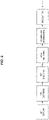
- FIGS. 1 to 3 are explanatory diagrams for explaining an example of a process in a transmission device that supports SPC.
- bit streams e.g., transport blocks
- some processes e.g., cyclic redundancy check (CRC) encoding, forward error correction (FEC) encoding, rate matching, and scrambling/interleaving, as illustrated in FIG. 2 ) are performed and then modulation is performed.
- CRC cyclic redundancy check
- FEC forward error correction
- layer mapping For example, layer mapping, power allocation, precoding, SPC multiplexing, resource element mapping, inverse discrete Fourier transform (IDFT)/inverse fast Fourier transform (IFFT), cyclic prefix (CP) insertion, digital-to-analog and radio frequency (RF) conversion, and the like are performed.
- IDFT inverse discrete Fourier transform
- IFFT inverse fast Fourier transform
- CP cyclic prefix
- RF radio frequency
- power allocation power is allocated to signals of the user A, the user B, and the user C, and in SPC multiplexing, the signals of the user A, the user B, and the user C are multiplexed.
- a cell-specific reference signal (CRS) and/or a UE-specific reference signal (UERS), for example, are transmitted in addition to the bit streams.
- CRS cell-specific reference signal
- UERS UE-specific reference signal
- the CRS and the UERS are transmitted respectively using different antenna ports.
- FIG. 4 is an explanatory diagram for explaining an example of a process in a reception device that performs interference cancellation.
- RF and analog-to-digital conversion, CP removal, discrete Fourier transform (DFT)/fast Fourier transform (FFT), joint interference cancellation, equalization, decoding, and the like are performed.
- This provides bit streams (e.g., transport blocks) of the user A, the user B, and the user C.
- HetNet heterogeneous network
- SCE small cell enhancement
- An index of a cell to be in connection with a target user u is denoted by i, and the number of transmission antennas of a base station corresponding to the cell is denoted by N TX,i .
- Each of the transmission antennas may also be called a transmission antenna port.
- a transmission signal from the cell i to the user u can be expressed in a vector form as below.
- N SS,u denotes the number of spatial transmission streams for the user u.
- N SS,u is a positive integer equal to or less than N TX,i .
- a vector x i,u is a spatial stream signal to the user u. Elements of this vector basically correspond to digital modulation symbols of phase shift keying (PSK), quadrature amplitude modulation (QAM), or the like.
- a matrix W i,u is a precoding matrix for the user u . An element in this matrix is basically a complex number, but may be a real number.
- a matrix P i,u is a power allocation coefficient matrix for the user u in the cell i.
- each element is preferably a positive real number.
- this matrix may be a diagonal matrix (i.e., a matrix whose components excluding diagonal components are zero) as below.
- P i , u P i , u , 0,0 0 ... 0 0 P i , u , 1,1 ⁇ ⁇ ⁇ ⁇ ⁇ 0 0 ... ... P i , u , N SS , u ⁇ 1 , N SS , u ⁇ 1
- a scalar value P i,u may be used instead of the matrix P i,u .
- U i denotes a set of users for which multiplexing is performed in the cell i .
- a transmission signal s j is generated similarly. Such a signal is received as interference at the user side.
- a reception signal r u of the user u can be expressed as below.
- a matrix H u,i is a channel response matrix for the cell i and the user u.
- Each element of the matrix H u,i is basically a complex number.
- a vector n u is noise included in the reception signal r u of the user u.
- the noise includes thermal noise and interference from another system.
- the average power of the noise is expressed as below. ⁇ n , u 2
- the reception signal r u can also be expressed by a desired signal and another signal as below.
- r u H u , i s i , u + H u , i ⁇ ⁇ ⁇ U i , ⁇ ⁇ u s i , ⁇ + ⁇ j ⁇ i H u , j ⁇ ⁇ ⁇ U j s j , ⁇ + n u
- the first term of the right side denotes a desired signal of the user u
- the second term interference in the serving cell i of the user u
- the third term interference from a cell other than the cell i (called inter-cell interference).
- the reception signal can be expressed as below.
- r u H u , i s i , u + ⁇ j ⁇ i H u , j s j , ⁇ + n u
- power is allocated not only to a data signal generated from a bit stream but also to a CRS and a UERS.
- power allocation may be performed individually on the data signal, the CRS, and the UERS, and multiplication of individual precoding matrixes may be performed.
- the same power allocation may be performed on the data signal and the UERS (i.e., the same power may be allocated to the data signal and the UERS).
- uplink transmission signals and reception signals when SPC is adopted will be described. Assumed here is a multi-cell system of HetNet, SCE, or the like. Note that the signs used for downlink will be further used as signs denoting signals and the like.
- a transmission signal that the user u transmits in the cell i can be expressed in a vector form as below.
- the number of transmission antennas is the number of transmission antennas of the user, N TX,u .
- a matrix P i,u which is a power allocation coefficient matrix for the user u in the cell i, may be a diagonal matrix.
- a reception signal of a base station of the cell i can be expressed as below.
- a base station needs to obtain all signals from a plurality of users in a cell by decoding. Note also that a channel response matrix differs depending on a user.
- a reception signal can be expressed as below.
- the first term of the right side denotes a desired signal of the user u
- the second term interference in the serving cell i of the user u
- the third term interference from a cell other than the cell i (called inter-cell interference).
- the reception signal can be expressed as below.
- r i , u H i , u s i , u + ⁇ j ⁇ i H i , ⁇ s j , ⁇ + n i
- FIG. 5 is an explanatory diagram illustrating an example of the schematic configuration of the system 1 according to an embodiment of the present disclosure.
- the system 1 includes a base station 100 and a terminal device 200.
- the terminal device 200 is also called a user.
- the user may also be called a user equipment (UE).
- the UE may be a UE defined in LTE or LTE-A, or may generally refer to communication equipment.
- the system 1 can of course include a plurality of terminal devices 200.
- the system 1 can also include other types of terminal devices in addition to the terminal device 200.
- “Another terminal device” may be another terminal device 200 or a terminal device of another type.
- the base station 100 is a base station of a cellular system (or mobile communication system).
- the base station 100 performs radio communication with a terminal device (e.g., the terminal device 200) located in a cell 101 of the base station 100.
- a terminal device e.g., the terminal device 200
- the base station 100 transmits a downlink signal to the terminal device, and receives an uplink signal from the terminal device.
- the terminal device 200 can perform communication in a cellular system (or mobile communication system).
- the terminal device 200 performs radio communication with a base station (e.g., the base station 100) of the cellular system.
- a base station e.g., the base station 100
- the terminal device 200 receives a downlink signal from the base station, and transmits an uplink signal to the base station.
- the base station 100 performs radio communication with a plurality of terminal devices by non-orthogonal multiple access.
- the base station 100 performs radio communication with the plurality of terminal devices by multiplexing/multiple access using SPC.
- the base station 100 performs radio communication with the plurality of terminal devices by multiplexing/multiple access using SPC in downlink. Specifically, for example, the base station 100 multiplexes data signals to the plurality of terminal devices using SPC. In this case, for example, the terminal device 200 removes one or more other data signals, as interference, from a multiplexed signal including a data signal to the terminal device 200, and decodes the resulting signal into the data signal to the terminal device 200.
- the base station 100 may perform radio communication with the plurality of terminal devices by multiplexing/multiple access using SPC in uplink, instead of or together with downlink.
- the base station 100 may decode a multiplexed signal including data signals transmitted from the plurality of terminal devices into the data signals.
- the base station 100 transmits a reference signal.
- the base station 100 transmits, for example, a reference signal unique to a cell (cell-specific reference signal or CRS) and a reference signal unique to a user (a user-specific reference signal).
- the reference signal unique to a user is, for example, a UE-specific reference signal (UERS).
- the UERS may be a UERS defined in LTE or LTE-A, or may be called a demodulation reference signal (DMRS).
- DMRS demodulation reference signal
- FIG. 6 is an explanatory diagram for describing a first example of transmission of a reference signal and a data signal.
- power of signals for a user U within a cell i is shown in the upper part
- power of signals for a user V within the cell i is shown in the lower part.
- power of CRSs, UERSs, and data signals is shown.
- the horizontal axis represents frequency and/or time resources
- the vertical axis represents power or power density per unit resource.
- radio resources (frequency and/or time resources) to be used in transmission of the data signals are different from radio resources (frequency and/or time resources) to be used in transmission of the CRSs and UERSs.
- radio resources (frequency and/or time resources) to be used in transmission of the CRSs are different from radio resources (frequency and/or time resources) to be used in transmission of the UERSs.
- the data signals for the different users are multiplexed using SPC. That is, the same radio resources are used in transmission of the data signals to the different users. Different levels of power are allocated to the data signals serving as a target for multiplexing.
- UERSs for the different users are multiplexed (for example, using SPC). That is, the same radio resources are used in transmission of the UERSs to the different users. Different levels of power are allocated to the UERSs serving as a target for multiplexing.
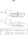
- FIG. 7 is an explanatory diagram for describing a second refinement of transmission of reference signals and data signals.
- radio resources to be used in transmission of a UERS to a user are not used in transmission of another signal in this example.
- radio resources to be used in transmission of the UERS to the user U are not used in transmission of the CRS, the data signal to the user U, the data signal to the user V, and the UERS to the user V.
- Radio resources to be used in transmission of the UERS to the user V are not used in transmission of the CRS, the data signal to the user V, the data signal to the user U, and the transmission of the UERS to the user U. Accordingly, for example, it is possible to enhance accuracy in channel estimation based on the UERS. However, radio resource use efficiency may be degraded.
- FIG. 8 is an explanatory diagram for describing a third refinement of transmission of reference signals and data signals.
- orthogonality between the UERSs is heightened due to adjustment of a phase pattern. For example, as a phase of the UERS for the user U becomes different from a phase of the UERS for the user V, by adjusting the phase of the UERS for the user U and the phase of the UERS for the user V, orthogonality between the UERS for the user U and the UERS for the user V can be heightened. Accordingly, for example, it is possible to enhance accuracy in channel estimation based on the UERSs.
- the base station 100 may transmit a CRS, but may not transmit a UERS.
- radio resources to be used in transmission of the UERS in FIGS. 6 to 8 may be used in transmission of a data signal, rather than transmission of the UERS.
- the base station 100 may transmit a UERS, but may not transmit a CRS.
- radio resources to be used in transmission of the CRS in FIGS. 6 to 8 may be used in transmission of a data signal, rather than transmission of the CRS.
- the base station 100 may transmit a UERS, but may not transmit a CRS on a secondary component carrier (SCC) of carrier aggregation.
- SCC secondary component carrier
- the SCC may be a component carrier (CC) that is used in transmission of a user plane but not used in transmission of a control plane.
- the base station 100 may transmit a UERS, but may not transmit a CRS in a period for transmission of a user plane. Note that the base station 100 may transmit a CRS in a period for transmission of a control plane.
- power is allocated to each of a plurality of data signals.
- a decision on power to be allocated to each of the plurality of data signals is performed by, for example, the base station 100. Note that, instead of the base station 100, the decision on power to be allocated to each of the plurality of data signals may be performed by another network node.
- the power P DATA,U of the data signal for the user U and the power P DATA,V of the data signal for the user V have the following relationships.
- P DATA , U > P DATA , V P DATA , U ⁇ P DATA , V ⁇ U , V
- the power P UERS,U of the UERS for the user U and the power P UERS,V of the UERS for the user V have the following relationships.
- P UERS , U > P UERS , V P UERS , U ⁇ P UERS , V ⁇ U , V
- the difference (or ratio) between the power of the data signal for the user U and the data signal for the user V be equal to the difference (or ratio) between the power of the UERS for the user U and the UERS for the user V.
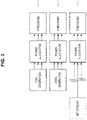
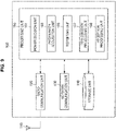
- FIG. 9 is a block diagram illustrating the example of the configuration of the base station 100 according to an embodiment of the present disclosure.
- the base station 100 includes an antenna unit 110, a radio communication unit 120, a network communication unit 130, a storage unit 140, and a processing unit 150.
- the antenna unit 110 radiates signals output by the radio communication unit 120 out into space as radio waves.
- the antenna unit 110 converts radio waves in the space into signals, and outputs the signals to the radio communication unit 120.
- the radio communication unit 120 transmits and receives signals. For example, the radio communication unit 120 transmits a downlink signal to a terminal device, and receives an uplink signal from a terminal device.
- the network communication unit 130 transmits and receives information.
- the network communication unit 130 transmits information to other nodes, and receives information from other nodes.
- the other nodes include another base station and a core network node.
- the storage unit 140 temporarily or permanently stores a program and various data for operation of the base station 100.
- the processing unit 150 provides various functions of the base station 100.
- the processing unit 150 includes a power decision unit 151, an information acquisition unit 153, a reporting unit 155, a transmission processing unit 157 and a reception processing unit 159.
- the processing unit 150 may further include a structural element other than these structural elements. That is, the processing unit 150 may perform operation other than the operation of these structural elements.
- FIG. 10 is a block diagram illustrating the example of the configuration of the terminal device 200 according to an embodiment of the present disclosure.
- the terminal device 200 includes an antenna unit 210, a radio communication unit 220, a storage unit 230, and a processing unit 240.
- the antenna unit 210 radiates signals output by the radio communication unit 220 out into space as radio waves. In addition, the antenna unit 210 converts radio waves in the space into signals, and outputs the signals to the radio communication unit 220.
- the radio communication unit 220 transmits and receives signals. For example, the radio communication unit 220 receives a downlink signal from a base station, and transmits an uplink signal to a base station.
- the storage unit 230 temporarily or permanently stores a program and various data for operation of the terminal device 200.
- the processing unit 240 provides various functions of the terminal device 200.
- the processing unit 240 includes an information acquisition unit 241, a transmission processing unit 243 and a reception processing unit 245. Note that the processing unit 240 may further include a structural element other than these structural elements. That is, the processing unit 240 may perform operation other than the operation of these structural elements.
- the base station 100 (the information acquisition unit 153) acquires information on power allocation to a data signal serving as a target for multiplexing using SPC (hereinbelow, will be referred to as "first allocation related information"). In addition, the base station 100 (the reporting unit 155) reports the first allocation related information to the terminal device 200.
- the terminal device 200 can ascertain reception power of the data signal included in a multiplexed signal.
- the terminal device 200 can appropriately decode the data signal.
- the data signal is a signal to the terminal device 200. More specifically, the data signal is, for example, a downlink data signal transmitted from the base station 100 to the terminal device 200.
- the data signal is, for example, a signal of a user plane.
- the data signal may be a signal of signaling of a control plane (for example, radio resource control (RRC) signaling, or non-access stratum (NAS) signaling).
- RRC radio resource control
- NAS non-access stratum
- the data signal and data signals for one or more other terminal devices are multiplexed using SPC, for example, and a multiplexed signal is transmitted.
- the first allocation related information is information indicating, for example, power allocated to the data signal.
- the power is power per unit resource (i.e., a power density).
- the first allocation related information is an index indicating the power allocated to the data signal. For example, a plurality of indices each indicating power are prepared, and power indicated by one index among the plurality of indices is allocated to the data signal. Then, the first allocation related information is the one index, and the base station 100 reports the one index to the terminal device 200. Due to the reporting of the index, for example, an amount of information necessary for reporting is reduced, and overhead is reduced.
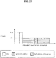
- FIG. 11 an example of a plurality of indices each indicating power will be described with reference to FIG. 11 .
- FIG. 11 is an explanatory diagram for describing an example of a plurality of indices each indicating power.
- N indices each indicating power are shown.
- An index 0, indicates P DATA,L (dBm) which is lower limit power
- an index 1 indicates P DATA,L +0.5 (dBm)
- an index 2 indicates P DATA,L +1.0 (dBm).
- An index N-1 indicates P DATA,H (dBm) which is upper limit power
- an index N-2 indicates P DATA,H -0.5 (dBm)
- an index N-3 indicates P DATA,H -1.0 (dBm).
- indices indicating power are prepared at increments of 0.5 dBm between P DATA,L and P DATA,H , and the first allocation related information indicates one of the indices 0 to N-1.
- the plurality of indices and power indicated by each of the plurality of indices are held in, for example, the terminal device 200. Accordingly, for example, the terminal device 200 can ascertain power from an index reported by the base station 100 to the terminal device 200.
- the first allocation related information may be a value of power allocated to the data signal, instead of such an index. Accordingly, for example, power can be allocated to the data signal more freely.
- the first allocation related information is information indicating a difference or a ratio between power allocated to the data signal and power allocated to another signal.
- the difference may be a difference in a decibel form, and the ratio may be a ratio in a linear form.
- the other signal may be a signal transmitted using the same antenna port as the data signal.
- the other signal may be a signal transmitted using the same one or more physical antenna elements as the data signal.
- the other signal is a reference signal.
- the reference signal may be a cell-specific reference signal (CRS).
- the first allocation related information may indicate the difference between power P DATA,U allocated to a data signal for the terminal device 200 (user U) and power P CRS allocated to the CRS.
- ⁇ CRS , U P CRS ⁇ P DATA , U
- the first allocation related information can indicate the difference as follows.
- ⁇ CRS , U P DATA , U ⁇ P CRS
- the reference signal is a user-specific reference signal.
- the user-specific reference signal may be a UERS.
- the user-specific reference signal may be a reference signal unique to the terminal device 200 (in other words, a reference signal unique to a user of the terminal device 200).
- the first allocation related information may indicate the difference between power P DATA,U allocated to a data signal for the terminal device 200 (user U) and power P UERS,U allocated to the user-specific reference signal (UERS) for the terminal device 200 as follows.
- ⁇ UERS , U P UERS ,U ⁇ P DATA , U
- the first allocation related information can indicate the difference as follows.
- ⁇ UERS , U P DATA , U ⁇ P UERS ,U
- the user-specific reference signal may be a reference signal unique to another terminal device (in other words, a reference signal unique to a user of the other terminal device).
- the first allocation related information may indicate the difference between power P DATA,U allocated to a data signal for the terminal device 200 (user U) and power P UERS,V allocated to a user-specific reference signal (UERS) for the other terminal device (user V) as follows.
- ⁇ UERS , U , V P UERS , V ⁇ P DATA , U
- the first allocation related information can indicate the difference as follows.
- ⁇ UERS , U , V P DATA , U ⁇ P UERS , V
- the power P DATA,U allocated to the data signal for the terminal device 200 (user U) and the power P UERS,V allocated to the user-specific reference signal (UERS) for the other terminal device (user V) may have one of the following two relationships.
- each of the differences has only a positive value or only a negative value.
- the reference signal may be a reference signal of another type (for example, a multimedia broadcast multicast service (MBMS) over single frequency network (MBSFN) RS, a channel state information (CSI) RS, or the like).
- MBMS multimedia broadcast multicast service
- MMSFN single frequency network
- CSI channel state information
- the other signal may be another data signal. More specifically, the other signal may be a data signal for another terminal device.
- the data signal for the terminal device 200 and data signals for one or more other terminal devices are multiplexed using SPC, and the other signal may be a data signal for one of the one or more other terminal devices.
- the first allocation related information may indicate the difference between the power P DATA,U allocated to the data signal for the terminal device 200 (user U) and power P DATA,V allocated to the data signal for the other terminal device (user V) as follows.
- ⁇ DATA , U , V P DATA , V ⁇ P DATA , U
- the first allocation related information can indicate the difference as follows.
- ⁇ DATA , U , V P DATA , U ⁇ P DATA , V
- the power P DATA,U allocated to the data signal for the terminal device 200 (user U) and the power P DATA,V allocated to the data signal for the other terminal device (user V) may have one of the following two relationships.
- each of the differences has only a positive value or only a negative value.
- the other signal may be a multiplexed signal including the data signal. More specifically, the data signal for the terminal device 200 and data signals for one or more other terminal devices are multiplexed using SPC, and the other signal may be a multiplexed signal including the data signal for the terminal device 200 and the data signals for the one or more terminal devices.
- the other signal may be a signal of a physical broadcast channel (PBCH), or a synchronization signal (for example, a primary synchronization signal (PSS), a secondary synchronization signal (SSS), or the like.
- PBCH physical broadcast channel
- PSS primary synchronization signal
- SSS secondary synchronization signal
- the first allocation related information may be an index indicating the difference or the ratio. Specifically, a plurality of indices each indicating a difference or a ratio of power are prepared, and the first allocation related information may be one index among the plurality of indices indicating a difference or a ratio between power allocated to the data signal and power allocated to the other signal.
- the base station 100 may report the one index to the terminal device 200. Through this reporting of the index, for example, an amount of information necessary for reporting is further reduced, and overhead is reduced.
- examples of a plurality of indices each indicating a difference of power will be described with reference to FIGS. 12 and 13 .
- FIG. 12 is an explanatory diagram for describing a first example of a plurality of indices each indicating a difference of power.
- N indices each indicating a difference of power are shown.
- An index 0, for example, indicates 0 (dBm) which is a lower limit difference
- an index 1 indicates 0.5 (dBm)
- an index 2 indicates 1.0 (dBm).
- An index N-1 for example, indicates 0.5 ⁇ (N-1) (dBm) which is an upper limit difference
- an index N-2 indicates 0.5 ⁇ (N-2) (dBm)
- an index N-3 indicates 0.5 ⁇ (N-3) (dBm).
- indices indicating differences at increments of 0.5 dBm are prepared between 0 (dBm) and 0.5 ⁇ (N-1) (dBm), and the first allocation related information indicates one of the indices 0 to N-1.
- N in the example of FIG. 12 may be the same as or different from N in the example of FIG. 11 .
- FIG. 13 is an explanatory diagram for describing a second refinement of a plurality of indices each indicating a difference of power.
- N indices each indicating a difference of power are shown.
- An index 0 indicates -0.5 ⁇ (N-1) (dBm) which is a lower limit difference
- an index 2 indicates -0.5 ⁇ (N-2) (dBm)
- an index 3 indicates -0.5 ⁇ (N-3) (dBm).
- An index N-1 for example, indicates 0 (dBm) which is an upper limit difference
- an index N-2 indicates -0.5 (dBm)
- an index N-3 indicates -1.0 (dBm).
- indices indicating differences are prepared at increments of 0.5 dBm between -0.5 ⁇ (N-1) (dBm) and 0 (dBm), and the first allocation related information indicates one of the indices 0 to N-1.
- N in the example of FIG. 13 may be the same as or different from N in the example of FIG. 11 .
- the plurality of indices and a difference or a ratio indicated by each of the plurality of indices are held in, for example, the terminal device 200. Accordingly, the terminal device 200 can, for example, ascertain a difference of power from an index reported by the base station 100 to the terminal device 200.
- the first allocation related information may be a value of the difference, instead of the index. Accordingly, for example, power can be allocated to the data signal more freely.
- the first allocation related information may be information indicating a difference or a ratio between power allocated to the data signal and power allocated to the other signal.
- a range of values that can be set for the difference or the ratio can be narrower than a range of values that can be set for the power allocated to the data signal.
- the base station 100 (the information acquisition unit 153) acquires, for example, other information on power allocation to a user-specific reference signal (hereinafter will be referred to as "second allocation related information"). Then, the base station 100 (the reporting unit 155) reports the second power allocation information to the terminal device 200.
- the user-specific reference signal is a reference signal unique to the terminal device 200.
- the user-specific reference signal is a user-specific reference signal for the terminal device 200.
- the user-specific reference signal is, for example, a UERS.
- the user-specific reference signal is a signal transmitted using the same antenna port as the data signal for the terminal device 200.
- the data signal is transmitted using the same antenna port as the user-specific reference signal (for example, UERS)
- the base station 100 reports the second allocation related information to the terminal device 200.
- the second allocation related information is, for example, information indicating power allocated to the user-specific reference signal.
- the power is power per unit resource (i.e., a power density).
- the second allocation related information is an index indicating the power allocated to the user-specific reference signal.
- a plurality of indices each indicating power are prepared, and power indicated by one index among the plurality of indices is allocated to the user-specific reference signal.
- the second allocation related information is the one index, and the base station 100 reports the one index to the terminal device 200. Through this reporting of the index, for example, an amount of information necessary for reporting is further reduced, and overhead is reduced.
- An example of a plurality of indices each indicating power will be described hereinbelow with reference to FIG. 14 .
- FIG. 14 is an explanatory diagram for describing an example of a plurality of indices each indicating power.
- N indices each indicating power are shown.
- An index 0, indicates P UERS,L (dBm) which is lower limit power
- an index 1 indicates P UERS,L +0.5 (dBm)
- an index 2 indicates P UERS,L +1.0 (dBm).
- An index N-1 indicates P UERS,H (dBm) which is upper limit power
- an index N-2 indicates P UERS,H -0.5 (dBm)
- an index N-3 indicates P UERS,H -1.0 (dBm).
- indices indicating power are prepared at increments of 0.5 dBm between P UERS,L and P UERS,H , and the second allocation related information indicates one of the indices 0 to N-1.
- N in the example of FIG. 14 may be the same as N in any one of the examples of FIGS. 11 , 12 , and 13 , or different from N in any one of the examples FIGS. 11 , 12 , and 13 .
- the plurality of indices and power indicated by each of the plurality of indices are held in, for example, the terminal device 200. Accordingly, for example, the terminal device 200 can ascertain power from an index reported by the base station 100 to the terminal device 200.
- the second allocation related information may be a value of power allocated to the user-specific reference signal, instead of the index. Accordingly, for example, power can be allocated to the data signal more freely.
- the second allocation related information may be information indicating the difference or ratio between power allocated to the user-specific reference signal and power allocated to another signal.
- the difference may be a difference in a decibel form, and the ratio may be a ratio in a linear form.
- the other signal may be a signal transmitted using the same antenna port as the user-specific reference signal.
- the other signal may be a signal transmitted using the same one or more physical antenna elements as the user-specific reference signal.
- the other signal may be a reference signal.
- the reference signal may be a cell-specific reference signal (CRS).
- the second allocation related information may indicate the difference between power P UERS,U allocated to a user-specific reference signal for the terminal device 200 (user U) and power P CRS allocated to a CRS as follows.
- ⁇ CRS , U P CRS ⁇ P UERS , U
- the second allocation related information may indicate the difference as follows.
- ⁇ CRS , U P UERS , U ⁇ P CRS
- the reference signal may be a user-specific reference signal for another terminal device (in other words, a reference signal unique to another terminal device).
- the user-specific reference signal may be a UERS.
- the second allocation related information may indicate the difference between power P UERS,U allocated to a user-specific reference signal (UERS) for the terminal device 200 (user U) and power P UERS,V allocated to the user-specific reference signal (UERS) for the other terminal device (user V) as follows.
- ⁇ UERS , U , V P UERS , V ⁇ P UERS , U
- the second allocation related information may indicate the difference as follows.
- ⁇ UERS , U , V P UERS , U ⁇ P UERS , V
- the power P UERS,U allocated to the user-specific reference signal for the terminal device 200 (user U) and the power P UERS,V allocated to the user-specific reference signal (UERS) for the other terminal device (user V) may have one of the following two relationships.
- each of the difference has only a positive value or only a negative value.
- the reference signal may be a reference signal of another type (for example, an MBSFN RS, a CSI RS, or the like).
- the other signal may be a data signal.
- the data signal may be the data signal for the terminal device 200.
- the second allocation related information may indicate the difference between the power P UERS,U allocated to the user-specific reference signal for the terminal device 200 (user U) and the power P DATA,U allocated to the data signal for the terminal device 200 (user U) as follows.
- ⁇ DATA , U P DATA ,U ⁇ P UERS , U
- the second allocation related information may indicate the difference as follows.
- ⁇ DATA , U P UERS , U ⁇ P DATA ,U
- the data signal may be a data signal for another terminal device.
- the data signal for the terminal device 200 and data signals for one or more other terminal devices are multiplexed using SPC, and the other signal may be a data signal for one of the one or more other terminal devices.
- the second allocation related information may indicate the difference between the power P UERS,U allocated to the user-specific reference signal for the terminal device 200 (user U) and the power P DATA,V allocated to the data signal for the other terminal device (user V) as follows.
- ⁇ DATA , U , V P DATA ,V ⁇ P UERS , U
- the second allocation related information may indicate the difference as follows.
- ⁇ DATA , U , V P UERS , U ⁇ P DATA ,V
- the power P UERS,U allocated to the user-specific reference signal for the terminal device 200 (user U) and the power P DATA,V allocated to the data signal for the other terminal device (user V) may have one of the following two relationships.
- each of the differences has only a positive value or a negative value.
- the other signal may be a multiplexed signal including the user-specific reference signal. More specifically, the user-specific reference signal for the terminal device 200 and user-specific reference signals for one or more other terminal devices are multiplexed using SPC, and the other signal may be the multiplexed signal including the user-specific reference signal for the terminal device 200 and the user-specific reference signals for the one or more other terminal devices.
- the second allocation related information may be an index indicating the difference or the ratio. Specifically, a plurality of indices each indicating a difference or a ratio of power are prepared, and the second allocation related information may be one index among the plurality of indices indicating a difference or a ratio between power allocated to the user-specific reference signal and power allocated to the other signal.
- the base station 100 may report the one index to the terminal device 200. Through this reporting of the index, for example, an amount of information necessary for reporting is further reduced, and overhead is reduced. Note that a specific example of the plurality of indices each indicating a difference of power is the same as those in the examples of FIGS. 12 and 13 .
- the plurality of indices and a difference or ratio indicated by each of the plurality of indices are held in, for example, the terminal device 200. Accordingly, for example, the terminal device 200 can ascertain the difference of power from an index reported by the base station 100 to the terminal device 200.
- the second allocation related information may be a value of the difference, instead of the index. Accordingly, for example, power can be allocated to the user-specific reference signals more freely.
- the second allocation related information may be information indicating a difference or ratio between power allocated to the user-specific reference signal and power allocated to the other signal.
- a range of values that can be set for the difference or the ratio can be narrower than a range of values that can be set for the power allocated to the user-specific reference signal.
- the base station 100 reports, to the terminal device 200, for example, the first allocation related information included in downlink control information for the terminal device 200.
- the first allocation related information is information on power allocation to a data signal (for example, a data signal for the terminal device 200) serving as a target for multiplexing using SPC.
- the downlink control information may be referred to as DCI.
- the base station 100 (the reporting unit 155) reports, for example, information indicating a power ranking of the data signal among a plurality of data signals serving as a target for multiplexing using SPC (hereinafter referred to as "ranking information") to the terminal device 200.
- ranking information information indicating a power ranking of the data signal among a plurality of data signals serving as a target for multiplexing using SPC
- the ranking information thereof indicates 0.
- the power level of the data signal is the lowest among the power levels of the M data signals (i.e., M power levels) serving as a target for multiplexing using SPC, for example, the ranking information thereof indicates M-1.
- the base station 100 (the reporting unit 155) reports, for example, the ranking information included in the downlink control information to the terminal device 200.
- the base station 100 (the reporting unit 155) reports, for example, the second allocation related information included in the downlink control information to the terminal device 200.
- the first allocation related information is information on power allocation to a user-specific reference signal (for example, a user-specific reference signal for the terminal device 200) as described above.
- the downlink control information has, for example, a format applicable to multiplexing using SPC.
- the format may also be called a DCI format.
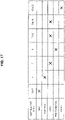
- FIG. 15 is an explanatory diagram for describing an example of information elements included in downlink control information. Referring to FIG. 15 , information elements that can be included in downlink control information according to the first embodiment are shown.
- Downlink control information includes, for example, one or more of a carrier indicator, a resource allocation header, a TPC command for uplink, a downlink assignment index, a HARQ process number, an antenna port, a scrambling pattern, an interleaving pattern, a layer, a sounding reference signal (SRS) request, a modulation and coding scheme (MCS), a new data indicator, and a redundancy version.
- SRS sounding reference signal
- MCS modulation and coding scheme
- the downlink control information includes, for example, SCH power, an SCH power offset from a UERS, or an SCH power offset from a CRS as the first allocation related information.
- SCH stands for a shared channel (SCH), and is, for example, a physical downlink shared channel (PDSCH) or a channel similar thereto.
- SCH power is power allocated to a data signal
- an SCH power offset from a UERS is the difference between power allocated to a data signal and power allocated to a UERS
- an SCH power offset from a CRS is the difference between power allocated to a data signal and power allocated to a CRS.
- the downlink control information includes, for example, UERS power, a UERS power offset from SCH, and a UERS power offset from CRS as the second allocation related information.
- UERS power is power allocated to a UERS
- a UERS power offset from an SCH is the difference between power allocated to a UERS and power allocated to a data signal
- a UERS power offset from a CRS is the difference between power allocated to a UERS and power allocated to a CRS.
- the downlink control information includes, for example, an SPC power ranking as the ranking information.
- the base station 100 may report, to the terminal device 200, the first allocation related information, the second allocation related information and/or the ranking information included in a signaling message (for example, RRC signaling) for the terminal device 200, instead of the downlink control information.
- the base station 100 may report, to the terminal device 200, the first allocation related information, the second allocation related information and the downlink control information/or the ranking information included in reporting information (for example, system information), instead of the downlink control information.
- the reporting unit 155 reports the first allocation related information to the terminal device 200.
- the transmission processing unit 157 transmits the report information generated by the reporting unit 155 to the terminal device 200 via, for example, the antenna unit 110 and the radio communication unit 120.
- the report information is, for example, the downlink control information for the terminal device 200.
- the report information may be the signaling message for the terminal device 200.
- the first allocation related information (i.e., information on power allocation to a data signal serving as a target for multiplexing using SPC) may be information in a form according to an antenna port to be used in transmission of the data signal.
- the data signal is, for example, a data signal for the terminal device 200.
- the base station 100 may select a form of the first allocation related information according to an antenna port to be used in transmission of the data signal.
- the first allocation related information may be in one of the following forms, as described above.
- the second allocation related information may also be information in a form according to such an antenna port.
- the user-specific reference signal is, for example, a user-specific reference signal for the terminal device 200 to be transmitted using the antenna port as described above.
- the user-specific reference signal is, for example, a UERS as described above.
- the base station 100 may select a form of the second allocation related information according to such an antenna port.
- the second allocation related information may be in one of the following forms as described above.
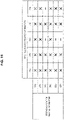
- Antenna ports to be used in transmission of a data signal vary depending on transmission modes (TMs). Examples of relationships of TMs and antenna ports will be described below with reference to FIG. 16 .
- FIG. 16 is an explanatory diagram for describing the examples of the relationships of transmission modes (TMs) and antenna ports.
- TMs transmission modes
- FIG. 16 (typical) transmission schemes used in the transmission modes 1 to 10 and antenna ports are shown.
- the transmission mode 2 for example, one or more of antenna ports 0 to 3 are used for transmission of a data signal.
- the transmission mode 5 one or more of antenna ports 1 to 5, 7, and 8 are used for transmission of a data signal.
- Reference signals to be transmitted vary depending on antenna ports. Examples of relationships of antenna ports and reference signals will be described below with reference to FIG. 17 .
- FIG. 17 is an explanatory diagram for describing examples of relationships of antenna ports and reference signals.
- reference signals each to be transmitted using antenna ports 0 to 22 are shown.
- a CRS is transmitted using, for example, antenna ports 0 to 3.
- a UERS is transmitted using antenna ports 5, and 7 to 14.
- an MBSFN RS is transmitted using an antenna port 4
- a positioning RS is transmitted using an antenna port 6
- a CSI RS is transmitted using antenna ports 15 to 22.
- a data signal for the terminal device 200 is transmitted using one of antenna ports 0 to 3. That is, the data signal for the terminal device 200 and a CRS are transmitted using the same antenna port.
- An example of first allocation related information in this case will be described below with reference to FIG. 18 .
- FIG. 18 is an explanatory diagram for describing examples of forms of first allocation related information in a case in which a data signal for the terminal device 200 and a CRS are transmitted using the same antenna port.
- the above-described (1A) to (1E) are shown as forms of the first allocation related information (i.e., information on power allocation to a data signal for the terminal device 200). Since an antenna port to be used in transmission of a CRS, for example, is not used in transmission of a UERS, in this case, (1C) and (1E) are not selected as a form of the first allocation related information.
- (1A) and (1B) may be selected as forms of the first allocation related information for a more stable operation. That is, the first allocation related information is information indicating power allocated to a data signal for the terminal device 200, or information indicating the difference between power allocated to a data signal for the terminal device 200 and power allocated to a CRS.
- the first allocation related information may be information indicating the difference between power allocated to a data signal for the terminal device 200 and power allocated to a data signal for another terminal device (for example, a data signal to be multiplexed with the data signal for the terminal device 200).
- the information indicating the power allocated to the data signal for the other terminal device i.e., information in a form similar to (1A)
- information indicating the difference between the power allocated to the data signal for the other terminal device and power allocated to the CRS i.e., information in a form similar to (1B)
- a data signal for the terminal device 200 is transmitted using one of antenna ports 5 and 7 to 14. That is, the data signal for the terminal device 200 and a UERS are transmitted using the same antenna port. Examples of forms of first allocation related information and second allocation related information in this case will be described below with reference to FIG. 19 .
- FIG. 19 is an explanatory diagram for describing examples of forms of first allocation related information and forms of second allocation related information in the case in which a data signal for the terminal device 200 and a UERS are transmitted using the same antenna port.
- the above-described (1A) to (1E) are shown as forms of the first allocation related information (i.e., information on power allocation to the data signal for the terminal device 200).
- the above-described (2A) to (2F) are shown as forms of the second allocation related information (i.e., information on power allocation to the UERS for the terminal device 200).
- (1C) is selected as a form of the first allocation related information
- (2C), (2E), and (2F) are not selected as forms of the second allocation related information.
- (1E) is selected as a form of the first allocation related information
- (2C) is not selected as a form of the second allocation related information.
- (1A) or (1C) may be selected as a form of the first allocation related information and (2A) may be selected as a form of the second allocation related information for a more stable operation.
- (1D) may be selected as a form of the first allocation related information. Description of this point is the same as in the example of FIG. 18 . Thus, overlapping description will not be provided.
- (2C) may be selected as a form of the second allocation related information.
- (2D) may be selected as a form of the second allocation related information. That is, the second allocation related information may be information indicating the difference between power allocated to a UERS for the terminal device 200 and power allocated to a UERS for another terminal device. In this case, information indicating the power allocated to the UERS of the other terminal device (i.e., information in a form similar to (2A)) may be reported to terminal devices including the terminal device 200.
- antenna ports used in transmission of a UERS are not used in transmission of a CRS
- an antenna port used in transmission of the UERS and an antenna port used in transmission of the CRS can correspond to the same physical antenna element.
- (1B) may be selected as a form of the first allocation related information
- (2B) may be selected as a form of the second allocation related information.
- the base station 100 decides on, for example, a level of power to be allocated to a data signal serving as a target for multiplexing using SPC.
- the data signal is, for example, a data signal for the terminal device 200.
- the first allocation related information is, for example, information indicating power allocated to the data signal as described above.
- the base station 100 the power decision unit 151 can more freely decide on a level of power to be allocated to the data signal in consideration of maximum transmission power.
- the first allocation related information is an index as described above, a level of power indicated by any index is decided on as the power to be allocated to the data signal.
- the first allocation related information may be information indicating the difference between power allocated to the data signal and power allocated to another signal as described above.
- the base station 100 the power decision unit 151 may decide on a level of power to be allocated to the data signal in consideration of power allocated to the other signal and maximum transmission power. Note that, when the first allocation related information is an index as described above, the difference between (or the sum of) a difference indicated by any index and power allocated to the other signal may be decided on as the power to be allocated to the data signal.
- the base station 100 (the power decision unit 151) also decides on a level of power to be allocated to a data signal for another terminal device.
- the base station 100 decides on, for example, a level of power to be allocated to a user-specific reference signal.
- the user-specific reference signal is, for example, a user-specific reference signal for the terminal device 200 (in other words, a reference signal unique to the terminal device 200), and is a UERS.
- the user-specific reference signal is, for example, a signal transmitted using the same antenna port as the data signal.
- the second allocation related information is, for example, information indicating power allocated to the user-specific reference signal as described above.
- the base station 100 the power decision unit 151 can more freely decide on a level of power to be allocated to the user-specific reference signal in consideration of maximum transmission power.
- the second allocation related information is an index as described above, a level of power indicated by any index may be decided on as the power to be allocated to the user-specific reference signal.
- the second allocation related information may be information indicating the difference between power allocated to the user-specific reference signal and power allocated to another signal as described above.
- the base station 100 the power decision unit 151 may decide on a level of power to be allocated to the user-specific reference signal in consideration of power allocated to the other signal and maximum transmission power.
- the second allocation related information is an index as described above, the difference between (or the sum of) a difference indicated by any index and the power allocated to the other signal may be decided on as the power to be allocated to the user-specific reference signal.
- the base station 100 (the power decision unit 151) of course decides on a level of power to be allocated to a user-specific reference signal for another terminal device as well.
- the base station 100 may also decide on a level of power to be allocated to another signal.
- the other signal may include a CRS and/or another reference signal (an MBSFN RS, a CSI RS, or the like).
- the base station 100 (the power decision unit 151) generates the first allocation related information (i.e., information on power allocation to the data signal) after, for example, the decision on power to be allocated to the data signal.
- the first allocation related information i.e., information on power allocation to the data signal
- the base station 100 (the power decision unit 151) generates the second allocation related information (i.e., information on power allocation to the user-specific reference signal) after, for example, the decision on power to be allocated to the user-specific reference signal.
- the second allocation related information i.e., information on power allocation to the user-specific reference signal
- the base station 100 (the transmission processing unit 157) allocates, for example, power decided on as described above to the data signal. Specifically, for example, the base station 100 (the transmission processing unit 157) allocates decided power to the data signal as illustrated in FIGS. 1 and 3 .
- the base station 100 (the transmission processing unit 157) allocates, for example, power decided on as described above to the user-specific reference signal (for example, a UERS). Specifically, for example, the base station 100 (the transmission processing unit 157) allocates the decided power to the user-specific reference signal (for example, a UERS) as illustrated in FIG. 3 .
- the user-specific reference signal for example, a UERS
- the terminal device 200 acquires information on power allocation to a data signal (i.e., first allocation related information) serving as a target for multiplexing using SPC.
- the terminal device 200 (the reception processing unit 245) decodes the data signal on the basis of the first allocation related information.
- the data signal is, for example, a data signal for the terminal device 200 as described above.
- the terminal device 200 (the reception processing unit 245), for example, computes reception power of the data signal on the basis of the allocation related information, and decodes the data signal on the basis of the reception power.
- the base station 100 reports the first allocation related information to the terminal device 200 as described above, and the terminal device 200 (the information acquisition unit 241) acquires the first allocation related information.
- the base station 100 reports, to the terminal device 200, for example, the first allocation related information included in downlink control information for the terminal device 200 as described above.
- the terminal device 200 (the information acquisition unit 241) acquires the first allocation related information from the downlink control information for the terminal device 200.
- the base station 100 may report the first allocation related information included in a signaling message for the terminal device 200 (for example, RRC signaling) to the terminal device 200, instead of the downlink control information as described above.
- the terminal device 200 (the information acquisition unit 241) may acquire the first allocation related information from the signaling message for the terminal device 200.
- the first allocation related information is, for example, information indicating power allocated to the data signal as described above.
- the terminal device 200 the reception processing unit 245) computes reception power of the data signal from the first allocation related information and path loss.
- the terminal device 200 (the reception processing unit 245) computes the path loss on the basis of, for example, power allocated to a reference signal transmitted using the same antenna port as the data signal (i.e., transmission power) and reception power of the reference signal.
- the reference signal is, for example, a CRS or a user-specific reference signal (for example, a UERS) for the terminal device 200.
- the terminal device 200 when the reference signal is the user-specific reference signal for the terminal device 200, the terminal device 200 (the reception processing unit 245) can ascertain the power allocated to the user-specific reference signal from the second allocation related information.
- the first allocation related information may be information indicating the difference or a ratio between power allocated to the data signal and power allocated to another signal.
- the terminal device 200 (the reception processing unit 245) may compute reception power of the data signal on the basis of the first allocation related information and reception power of the other signal.
- the other signal may be a reference signal (for example, a CRS, a user-specific reference signal, or the like), another data signal, a multiplexed signal including the data signal, or the like as described above.
- a reference signal for example, a CRS, a user-specific reference signal, or the like
- another data signal for example, a multiplexed signal including the data signal, or the like as described above.
- the terminal device 200 (the reception processing unit 245), for example, removes one or more other data signals among a plurality of pieces of data included in a multiplexed signal including the data signal from the multiplexed signal as interference, and decodes the data signal.
- the terminal device 200 When there is another data signal whose reception power is greater than a threshold value corresponding to reception power of the data signal among the plurality of data signals, for example, the terminal device 200 (the reception processing unit 245) removes one or more other data signals from the multiplexed signal as interference.
- the threshold value is a value smaller than the reception power of the data signal by a predetermined value.
- the terminal device 200 when there is no other data signal whose reception power is greater than the threshold value among the plurality of data signals, for example, the terminal device 200 (the reception processing unit 245) decodes the data signal without interference cancellation.
- the terminal device 200 the reception processing unit 245 decodes the data signal without interference cancellation.
- the reason for this is that interference of the other data signals hardly affects decoding of the data signal.
- the terminal device 200 acquires, for example, information on power allocation to each of one or more other data signals serving as a target for multiplexing with the data signal for the terminal device 200, similarly to the data signal for the terminal device 200. Then, the terminal device 200 (the information acquisition unit 241) computes reception power of each of the one or more other data signals, similarly to the data signal for the terminal device 200.
- the terminal device 200 sequentially removes, for example, one or more other data signals whose reception power is greater than that of the data signal among the plurality of data signals included in the multiplexed signal from the multiplexed signal as interference. Specifically, the terminal device 200 (the reception processing unit 245) performs, for example, successive interference cancellation (SIC).
- SIC successive interference cancellation
- the one or more other data signals are, for example, signals whose reception power is greater than that of the data signal by a predetermined amount of power or more. The reason for this is that the other data signals having greater reception power have higher communication quality and the other data signals are highly likely to be removed as interference by being correctly decoded.
- the terminal device 200 acquires, for example, information indicating a power ranking of the data signal (i.e., ranking information) among the plurality of data signals serving as a target for multiplexing. Then, the terminal device 200 (the reception processing unit 245) sequentially removes the one or more other signals from the multiplexed signal as interference on the basis of the ranking information.
- the base station 100 reports, for example, the ranking information to the terminal device 200 as described above, and the terminal device 200 (the information acquisition unit 241) acquires the ranking information.
- the power ranking indicated by the ranking information can be said to mean, for example, an order of a sequential process.
- the terminal device 200 determines to sequentially remove one or more other data signals from the multiplexed signal as interference. Then, the terminal device 200 (the reception processing unit 245) sequentially removes one or more other data signals whose reception power is greater than that of the data signal for the terminal device 200 from the multiplexed signal as interference. The terminal device 200 (the reception processing unit 245) sequentially removes the one or more other data signals as interference in, for example, reception power descending order.
- the terminal device 200 may acquire ranking information on each of the plurality of data signals.
- the terminal device 200 (the reception processing unit 245) may sequentially remove one or more other data signals with higher power rankings than the data signal for the terminal device 200 from the multiplexed signal as interference.
- the terminal device 200 (the reception processing unit 245) may sequentially remove the one or more other data signals in power ranking descending order as interference.
- the terminal device 200 may determine whether one or more other data signals are to be sequentially removed from the multiplexed signal as interference on the basis of reception power of the plurality of data signals included in the multiplexed signal. As an example, when the difference in reception power between the plurality of data signals exceeds a threshold value, the base station 100 may determine to sequentially remove one or more other data signals from the multiplexed signal as interference. Then, the terminal device 200 (the reception processing unit 245) may sequentially remove one or more other data signals whose reception power is greater than the data signal for the terminal device 200 from the multiplexed signal as interference. The terminal device 200 may sequentially remove the one or more other data signals in reception power descending order as interference.
- the terminal device 200 may remove one or more other data signals among the plurality of data signals included in the multiplexed signal from the multiplexed signal as interference in parallel. Specifically, the terminal device 200 (the reception processing unit 245) may perform parallel interference cancellation (PIC). Alternatively, the terminal device 200 (the reception processing unit 245) may perform elementary signal estimation (ESE). A technique including PIC, ESE, and the like can be called multi-user detection (MUD).
- PIC parallel interference cancellation
- ESE elementary signal estimation
- a technique including PIC, ESE, and the like can be called multi-user detection (MUD).
- the terminal device 200 may remove the one or more other data signals from the multiplexed signal as interference in parallel.
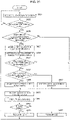
- FIG. 20 is a sequence diagram showing an example of a schematic flow of an overall process according to the first embodiment.
- the base station 100 performs scheduling (S601). That is, the base station 100 allocates radio resources to terminal devices. In particular, the base station 100 allocates radio resources to the terminal device 200 for transmission of a data signal (downlink signal) for the terminal device 200. The base station 100 also allocates such radio resources for transmission of one or more other data signals (for example, data signals for one or more other terminal devices).
- the base station 100 decides on a level of power to be allocated to the data signal for the terminal device 200 (S603).
- the base station 100 also decides on a level of power to be allocated to the one or more other data signals.
- the base station 100 (the power decision unit 151) generates first allocation related information (i.e., information on power allocation to the data signal) (S605).
- the base station 100 also generates information on power allocation to the one or more other data signals.
- the base station 100 (the information acquisition unit 153) obtains the first allocation related information, and the base station 100 (the reporting unit 155) reports, to the terminal device 200, the first allocation related information included in downlink control information for the terminal device 200 (S607). That is, the base station 100 transmits the downlink control information including the first allocation related information. Further, the base station 100 (the transmission processing unit 157) multiplexes the data signal for the terminal device 200 and the one or more other data signals using SPC, and transmits the multiplexed signal (S609). Further, the base station 100 (the transmission processing unit 157) also transmits a reference signal (S611).
- the terminal device 200 acquires the first allocation related information from the downlink control information, and decodes the data signal for the terminal device 200 on the basis of the first allocation related information (S613). Then, the terminal device 200 transmits an acknowledgement (ACK) or a negative acknowledgement (NACK) to the base station 100 (S615).
- ACK acknowledgement
- NACK negative acknowledgement
- FIG. 21 is a flowchart showing an example of a schematic flow of the decoding process of the terminal device 200 according to the first embodiment.
- the decoding process corresponds to Steps S613 and S615 of FIG. 20 .
- the terminal device 200 decodes the downlink control information (S621).
- the terminal device 200 checks whether there is a data signal for the terminal device 200 in the downlink control information (S623). If there is no data signal for the terminal device 200 (No in S623), the process returns to Step S621.
- the terminal device 200 checks whether a plurality of data signals (including the data signal for the terminal device 200) have been multiplexed on the same radio resource (S625).
- the terminal device 200 acquires information on power allocation to the data signal for the terminal device 200 (i.e., first allocation related information) from the downlink control information (S627).
- the terminal device 200 also acquires, for example, information on power allocation to one or more other data signals among the plurality of data signals.
- the terminal device 200 may also acquire information on power allocation to the user-specific reference signal (i.e., second allocation related information).
- the terminal device 200 (the reception processing unit 245) computes reception power of the plurality of data signals (S629). In particular, the terminal device 200 computes reception power of the data signal for the terminal device 200 on the basis of the first allocation related information.
- the terminal device 200 determines whether other data signals multiplexed with the data signal for the terminal device 200 are to be removed as interference (S631).
- the terminal device 200 determines whether the other data signals are to be sequentially removed (S633).
- the terminal device 200 determines whether the other data signals are determined to be sequentially removed (Yes in S633). If the other data signals are determined to be sequentially removed (Yes in S633), the terminal device 200 (the reception processing unit 245) sequentially removes the other data signals (S635). If not (No in S633), the terminal device 200 (the reception processing unit 245) removes the other data signals in parallel (S637). Then, the terminal device 200 (the reception processing unit 245) decodes the data signal for the terminal device 200 (S639).
- the terminal device 200 decodes the data signal for the terminal device 200 (without interference cancellation) (S639).
- the terminal device 200 After decoding of the data signal for the terminal device 200, the terminal device 200 (the reception processing unit 245) performs CRC checking (S641). If there is an error as a result (Yes in S643), the terminal device 200 transmits a NACK to the base station 100 (S645), or if there is no error (No in S643), the terminal device 200 transmits an ACK to the base station 100 (S647). Then, the process returns to Step S621.
- FIG. 22 is a flowchart showing an example of a schematic flow of a first determination process of the terminal device 200 according to the first embodiment.
- the first determination process is a process of determining whether other data signals are to be removed as interference, and corresponds to Step S631 in the example of FIG. 21 .
- the terminal device 200 determines whether there are other data signals whose reception power is greater than a threshold value that corresponds to reception power of the data signal for the terminal device among the plurality of data signals included in the multiplexed signal (S661).
- the terminal device 200 determines that the other data signals are to be removed as interference (S663). Then, the process ends.
- the terminal device 200 determines that the other data signals are not to be removed as interference (S665). Then, the process ends.
- FIG. 23 is a flowchart showing an example of a schematic flow of a second determination process of the terminal device 200 according to the first embodiment.
- the second determination process is a process of determining whether other data signals are to be sequentially removed as interference, and corresponds to Step S633 in the example of FIG. 21 .
- the terminal device 200 determines that the other data signals are to be sequentially removed as interference (S685).
- the terminal device 200 determines that the other data signals are to be sequentially removed as interference (S685). Then, the process ends.
- the terminal device 200 determines that the other data signals are to be removed in parallel as interference (S687). Then, the process ends.
- FIG. 24 is a flowchart showing an example of a schematic flow of a reception power computation process of the terminal device 200 according to the first embodiment.
- the reception power computation process corresponds to Step S629 in the example of FIG. 21 .
- the terminal device 200 acquires the first allocation related information (S701).
- the terminal device 200 determines whether the first allocation related information indicates power allocated to the data signal for the terminal device 200 (Yes in S703). If the first allocation related information indicates power allocated to the data signal for the terminal device 200 (Yes in S703), the terminal device 200 (the reception processing unit 245) computes reception power of the data signal for the terminal device 200 on the basis of the first allocation related information (and path loss) (S705). Then, the process ends.
- the terminal device 200 (the reception processing unit 245) computes reception power of the data signal for the terminal device 200 on the basis of the first allocation related information and reception power of the CRS (S709). Then, the process ends.
- the terminal device 200 (the reception processing unit 245) computes reception power of the data signal for the terminal device 200 on the basis of the first allocation related information and reception power of the UERS (S711). Then, the process ends.
- a data signal serving as a target for multiplexing using SPC is a data signal for the terminal device 200 (i.e., a downlink signal) in the above-described first embodiment
- the first embodiment is not limited thereto.
- a data signal serving as a target for multiplexing using SPC may be a data signal from the terminal device 200 (i.e., an uplink signal).
- the terminal device 200 may acquire such first allocation related information. Then, the terminal device 200 (the transmission processing unit 243) may allocate power to a data signal from the terminal device 200 (i.e., an uplink signal) on the basis of the first allocation related information.
- the base station 100 may acquire such first allocation related information. Then, the base station 100 (the reporting unit 155) may report the first allocation related information to the terminal device 200.
- the base station 100 may decode the data signal from the terminal device 200 on the basis of the first allocation related information.
- the base station 100 can cause the terminal device 200 to allocate power of a desired level to the data signal and can ascertain reception power of the data signal included in the multiplexed signal.
- the base station 100 can appropriately decode the data signal.
- FIG. 25 is a sequence diagram showing an example of a schematic flow of an overall process according to the modified example of the first embodiment.
- the base station 100 performs scheduling (S721). That is, the base station 100 allocates radio resources to terminal devices. In particular, the base station 100 allocates radio resources to the terminal device 200 for transmission of a data signal from the terminal device 200 (an uplink signal). In addition, the base station 100 also allocates such radio resources for transmission of one or more other data signals (for example, data signals from one or more other terminal devices).
- the base station 100 decides on a level of power to be allocated to the data signal from the terminal device 200 (S723).
- the base station 100 also decides on a level of power to be allocated to the one or more other data signals.
- the base station 100 (the power decision unit 151) generates first allocation related information (i.e., information on power allocation to the data signal) (S725).
- the base station 100 also generates information on power allocation to the one or more other data signals.
- the base station 100 (the information acquisition unit 153) obtains the first allocation related information, the base station 100 (the reporting unit 155) reports, to the terminal device 200, the first allocation related information included in downlink control information for the terminal device 200 (S727). That is, the base station 100 transmits the downlink control information including the first allocation related information. Further, the base station 100 (the transmission processing unit 157) also transmits a reference signal (S729).
- the terminal device 200 acquires the first allocation related information from the downlink control information, and the terminal device 200 (the transmission processing unit 243) transmits the data signal from the terminal device 200 on the basis of the first allocation related information (S731). In particular, the terminal device 200 (the transmission processing unit 243) allocates power to the data signal from the terminal device 200 on the basis of the first allocation related information.
- the base station 100 acquires the first allocation related information, and decodes the data signal from the terminal device 200 on the basis of the first allocation related information (S733). Note that the base station 100 (the information acquisition unit 153) also acquires information on power allocation to each of one or more other data signals multiplexed with the data signal from the terminal device 200, and decodes the one or more other data signals on the basis of the information.
- the base station 100 transmits an ACK or a NACK to the terminal device 200 (S735).
- FIG. 26 is a flowchart showing an example of a schematic flow of a decoding process of the base station 100 according to the modified example of the first embodiment.
- the decoding process corresponds to Steps S733 and S735 in the example of FIG. 25 .
- the base station 100 If decoding of a plurality of data signals is unnecessary (No in S741), the base station 100 (the reception processing unit 159) decodes a single data signal (S753).
- the base station 100 If decoding of a plurality of data signals is necessary (Yes in S741) and the plurality of data signals have not been multiplexed on the same radio resource (No in S743), the base station 100 (the reception processing unit 159) decodes each of the plurality of data signals (S751).
- the base station 100 determines whether the plurality of data signals are to be sequentially decoded (S745).
- the base station 100 determines whether the plurality of data signals are determined to be sequentially decoded (Yes in S745). If the plurality of data signals are determined to be sequentially decoded (Yes in S745), the base station 100 (the reception processing unit 159) sequentially decodes the plurality of data signals (S747). If not (No in S745), the base station 100 (the reception processing unit 159) decodes the plurality of data signals in parallel (S749).
- the base station 100 After decoding, the base station 100 (the reception processing unit 159) performs CRC checking (S755). If there is an error as a result (Yes in S757), the base station 100 transmits a NACK to the terminal device 200 (S759), or if there is no error (No in S757), the base station 100 transmits an ACK to the base station 100 (S761). Then, the process returns to Step S741.
- the plurality of data signals to be decoded include the data signal from the terminal device 200, and the single data signal to be decoded is the data signal from the terminal device 200.
- the base station 100 decides on a level of power to be allocated to a data signal for the terminal device 200 serving as a target for multiplexing using SPC and a reference signal unique to the terminal device 200 (in other words, a user-specific reference signal for the terminal device 200).
- the difference or ratio between the power allocated to the data signal and the power allocated to the reference signal is a predetermined difference or ratio.
- the reference signal is, for example, a reference signal transmitted using the same antenna port as the data signal.
- the reference signal is, for example, a UERS for the terminal device 200.
- the predetermined difference is, for example, 0, and the predetermined ratio is 1:1. That is, the power allocated to the data signal is the same as the power allocated to the reference signal. A specific example of this point will be described below with reference to FIG. 27 .
- FIG. 27 is an explanatory diagram for describing a first refinement of power allocation according to the further example.
- power allocated to a CRS, UERS for the user U (the terminal device 200), and a data signal for the user U (the terminal device 200) are shown.
- the horizontal axis represents frequency and/or time resources, and the vertical axis represents power or power density per unit resource.
- the power allocated to the CRS is, for example, P CRS .
- the power allocated to the UERS for the user U is P U
- the power allocated to the data signal for the user U is also P U .
- the predetermined difference is not limited to 0, and the predetermined ratio is not limited to 1:1. That is, the power allocated to the data signal may not be the same as power allocated to the reference signal.
- the predetermined difference may be another value (for example, 0.5 dBm, or the like), and the predetermined ratio may be another ratio (for example, 2:3, or the like).
- the terminal device 200 can ascertain reception power of the data signal included in the multiplexed signal from reception power of the reference signal.
- the terminal device 200 can appropriately decode the data signal. Furthermore, since reporting of information on power allocation to the data signal, for example, is unnecessary, overhead can be reduced.
- the terminal device 200 decodes the data signal for the terminal device 200 serving as a target for multiplexing using SPC on the basis of reception power of a reference signal unique to the terminal device.
- the difference or ratio between power allocated to the data signal and power allocated to the reference signal is a predetermined difference or ratio.
- the predetermined difference is, for example, 0, or the predetermined ratio is 1:1. That is, power allocated to the data signal is the same as power allocated to the reference signal.
- the terminal device 200 (the reception processing unit 245) deems the reception power of the reference signal as the reception power of the data signal.
- the terminal device 200 (the reception processing unit 245) decodes the data signal for the terminal device 200 on the basis of the reception power of the data signal (i.e., the reception power of the reference signal).
- power allocated to the data signal may not be the same as power allocated to the reference signal.
- the terminal device 200 (the reception processing unit 245) may compute reception power of the data signal from reception power of the reference signal, and may decode the data signal for the terminal device 200 on the basis of the reception power of the data signal.
- the base station 100 decides on a level of power to be allocated to a data signal for each of a plurality of terminal devices serving as a target for multiplexing using SPC, and a level of power allocated to a reference signal unique to each of the plurality of terminal devices.
- the difference or ratio between power allocated to the data signal for the terminal device and power allocated to the reference signal unique to the terminal device is the same difference or ratio.
- the reference signal is, for example, a reference signal transmitted using the same antenna port as the data signal.
- the reference signal is, for example, a UERS.
- a reference signal unique to each of the plurality of terminal devices are, in other words, a user-specific reference signal for each of the plurality of terminal devices.
- a UERS for the user U (the terminal device 200), a data signal for the user U (the terminal device 200), a UERS for the user V (another terminal device), and a data signal for the user U (the other terminal device) is shown.
- the difference between power P DATA,U allocated to the data signal for the user U (the terminal device 200) and power P UERS,U allocated to the UERS for the user U (the terminal device 200) is, for example, D (dBm).
- the difference between power P DATA,V allocated to the data signal for the user V (the other terminal device) and power P UERS,V allocated to the UERS for the user V (the other terminal device) is also D (dBm).
- the terminal device 200 can ascertain reception power of each of the plurality of data signals included in a multiplexed signal from reception power of each of the plurality of reference signals.
- the terminal device 200 can appropriately decode the data signals. Furthermore, since reporting of information on power allocation to the data signals is unnecessary, for example, overhead can be reduced.
- the terminal device 200 decodes a data signal for a target terminal device (the terminal device 200) among data signals for a plurality of terminal devices serving as a target for multiplexing using SPC on the basis of reception power of a reference signal unique to each of the plurality of terminal devices.
- the difference or ratio between power allocated to a data signal for a terminal device and power allocated to a reference signal unique to a terminal device is the same difference or ratio.
- the ratio between the sum of reception power of the reference signals and reception power of a reference signal unique to the terminal device 200 is, for example, equal to the ratio between reception power of a multiplexed signal and reception power of a data signal for the terminal device 200.
- the terminal device 200 (the reception processing unit 245) computes reception power of the data signal for the terminal device 200 from reception power of a reference signal unique to each of the plurality of terminal devices and the reception power of the multiplexed signal including the data signal for the terminal device 200. Then, the terminal device 200 (the reception processing unit 245) decodes the data signal for the terminal device 200 on the basis of the reception power of the data signal for the terminal device 200.
- FIG. 28 is a sequence diagram showing an example of a schematic flow of an overall process according to the further example.
- the base station 100 performs scheduling (S781). That is, the base station 100 allocates radio resources to terminal devices. For example, the base station 100 allocates radio resources to each of a plurality of terminal devices including the terminal device 200. The base station 100 allocates the radio resources for, for example, transmission of data signals to each of the plurality of terminal devices.
- the base station 100 decides on a level of power to be allocated to the data signal for each of the plurality of terminal devices (S783).
- the base station 10 the transmission processing unit 157) 0, the base station 100 transmits downlink control information to each of the plurality of terminal devices (S785). Further, the base station 100 (the transmission processing unit 157) multiplexes the data signals for the plurality of terminal devices using SPC, and transmits a multiplexed signal (S787). Further, the base station 100 (the transmission processing unit 157) also transmits UERSs to each of the plurality of terminal devices (S789).
- the terminal device 200 decodes a data signal for the terminal device 200 on the basis of reception power of the UERS for the terminal device 200 (S791). As a first refinement, the terminal device 200 (the reception processing unit 245) decodes the data signal for the terminal device 200 on the basis of the reception power of the UERS for the terminal device 200. As a second refinement, the terminal device 200 (the reception processing unit 245) decodes the data signal for the terminal device 200 on the basis of reception power of the UERS for each of the plurality of terminal devices.
- the terminal device 200 transmits an acknowledgement (ACK) or a negative acknowledgement (NACK) to the base station 100 (S793).
- ACK acknowledgement
- NACK negative acknowledgement
- the base station 100 may be realized as any type of evolved node B (eNB), for example, a macro eNB, a small eNB, or the like.
- eNB evolved node B
- a small eNB may be an eNB that covers a smaller cell than a macro cell, such as a pico eNB, a micro eNB, or a home (femto) eNB.
- the base station 100 may be realized as another type of base station such as a node B or a base transceiver station (BTS).
- BTS base transceiver station
- the base station 100 may include a main body that controls radio communication (also referred to as a base station device) and one or more remote radio heads (RRHs) disposed in a different place from the main body.
- a main body that controls radio communication also referred to as a base station device
- RRHs remote radio heads
- various types of terminals to be described below may operate as the base station 100 by temporarily or semi-permanently executing the base station function.
- at least some of constituent elements of the base station 100 may be realized in a base station device or a module for a base station device.
- the terminal device 200 may be realized as, for example, a mobile terminal such as a smartphone, a tablet personal computer (PC), a notebook PC, a portable game terminal, a portable/dongle type mobile router, or a digital camera, or an in-vehicle terminal such as a car navigation device.
- the terminal device 200 may be realized as a terminal that performs machine-to-machine (M2M) communication (also referred to as a machine type communication (MTC) terminal).
- M2M machine-to-machine
- MTC machine type communication
- at least some of constituent elements of the terminal device 200 may be realized in a module mounted in such a terminal (for example, an integrated circuit module configured in one die).
- FIG. 29 is a block diagram illustrating a first refinement of a schematic configuration of an eNB to which the technology of the present disclosure may be applied.
- An eNB 800 includes one or more antennas 810 and a base station device 820. Each antenna 810 and the base station device 820 may be connected to each other via an RF cable.
- Each of the antennas 810 includes a single or multiple antenna elements (such as multiple antenna elements included in an MIMO antenna), and is used for the base station device 820 to transmit and receive radio signals.
- the eNB 800 may include the multiple antennas 810, as illustrated in FIG. 29 .
- the multiple antennas 810 may be compatible with multiple frequency bands used by the eNB 800.
- FIG. 29 illustrates the example in which the eNB 800 includes the multiple antennas 810, the eNB 800 may also include a single antenna 810.
- the base station device 820 includes a controller 821, a memory 822, a network interface 823, and a radio communication interface 825.
- the controller 821 may be, for example, a CPU or a DSP, and operates various functions of a higher layer of the base station device 820. For example, the controller 821 generates a data packet from data in signals processed by the radio communication interface 825, and transfers the generated packet via the network interface 823. The controller 821 may bundle data from multiple base band processors to generate the bundled packet, and transfer the generated bundled packet. The controller 821 may have logical functions of performing control such as radio resource control, radio bearer control, mobility management, admission control, and scheduling. The control may be performed in corporation with an eNB or a core network node in the vicinity.
- the memory 822 includes RAM and ROM, and stores a program that is executed by the controller 821, and various types of control data (such as a terminal list, transmission power data, and scheduling data).
- the network interface 823 is a communication interface for connecting the base station device 820 to a core network 824.
- the controller 821 may communicate with a core network node or another eNB via the network interface 823.
- the eNB 800, and the core network node or the other eNB may be connected to each other through a logical interface (such as an S1 interface and an X2 interface).
- the network interface 823 may also be a wired communication interface or a radio communication interface for radio backhaul. If the network interface 823 is a radio communication interface, the network interface 823 may use a higher frequency band for radio communication than a frequency band used by the radio communication interface 825.
- the radio communication interface 825 supports any cellular communication scheme such as Long Term Evolution (LTE) and LTE-Advanced, and provides radio connection to a terminal positioned in a cell of the eNB 800 via the antenna 810.
- the radio communication interface 825 may typically include, for example, a baseband (BB) processor 826 and an RF circuit 827.
- the BB processor 826 may perform, for example, encoding/decoding, modulating/demodulating, and multiplexing/demultiplexing, and performs various types of signal processing of layers (such as L1, medium access control (MAC), radio link control (RLC), and a packet data convergence protocol (PDCP)).
- the BB processor 826 may have a part or all of the above-described logical functions instead of the controller 821.
- the BB processor 826 may be a memory that stores a communication control program, or a module that includes a processor and a related circuit configured to execute the program. Updating the program may allow the functions of the BB processor 826 to be changed.
- the module may be a card or a blade that is inserted into a slot of the base station device 820. Alternatively, the module may also be a chip that is mounted on the card or the blade.
- the RF circuit 827 may include, for example, a mixer, a filter, and an amplifier, and transmits and receives radio signals via the antenna 810.
- the radio communication interface 825 may include the multiple BB processors 826, as illustrated in FIG. 29 .
- the multiple BB processors 826 may be compatible with multiple frequency bands used by the eNB 800.
- the radio communication interface 825 may include the multiple RF circuits 827, as illustrated in FIG. 29 .
- the multiple RF circuits 827 may be compatible with multiple antenna elements.
- FIG. 29 illustrates the example in which the radio communication interface 825 includes the multiple BB processors 826 and the multiple RF circuits 827, the radio communication interface 825 may also include a single BB processor 826 or a single RF circuit 827.
- one or more structural elements included in the processing unit 150 may be implemented by the radio communication interface 825.
- the radio communication interface 825 may be implemented by the radio communication interface 825.
- the controller 821 may be implemented by the one or more structural elements.
- the module may store a program for causing the processor to function as the one or more structural elements (i.e., a program for causing the processor to execute operations of the one or more structural elements) and may execute the program.
- the program for causing the processor to function as the one or more structural elements may be installed in the eNB 800, and the radio communication interface 825 (for example, the BB processor 826) and/or the controller 821 may execute the program.
- the eNB 800, the base station device 820, or the module may be provided as a device which includes the one or more structural elements, and the program for causing the processor to function as the one or more structural elements may be provided.
- a readable recording medium in which the program is recorded may be provided.
- the radio communication unit 120 described with reference to FIG. 9 may be implemented by the radio communication interface 825 (for example, the RF circuit 827).
- the antenna unit 110 may be implemented by the antenna 810.
- the network communication unit 130 may be implemented by the controller 821 and/or the network interface 823.
- FIG. 30 is a block diagram illustrating a second refinement of a schematic configuration of an eNB to which the technology of the present disclosure may be applied.
- An eNB 830 includes one or more antennas 840, a base station device 850, and an RRH 860. Each antenna 840 and the RRH 860 may be connected to each other via an RF cable. The base station device 850 and the RRH 860 may be connected to each other via a high speed line such as an optical fiber cable.
- Each of the antennas 840 includes a single or multiple antenna elements (such as multiple antenna elements included in an MIMO antenna), and is used for the RRH 860 to transmit and receive radio signals.
- the eNB 830 may include the multiple antennas 840, as illustrated in FIG. 30 .
- the multiple antennas 840 may be compatible with multiple frequency bands used by the eNB 830.
- FIG. 30 illustrates the example in which the eNB 830 includes the multiple antennas 840, the eNB 830 may also include a single antenna 840.
- the base station device 850 includes a controller 851, a memory 852, a network interface 853, a radio communication interface 855, and a connection interface 857.
- the controller 851, the memory 852, and the network interface 853 are the same as the controller 821, the memory 822, and the network interface 823 described with reference to FIG. 29 .
- the radio communication interface 855 supports any cellular communication scheme such as LTE and LTE-Advanced, and provides radio communication to a terminal positioned in a sector corresponding to the RRH 860 via the RRH 860 and the antenna 840.
- the radio communication interface 855 may typically include, for example, a BB processor 856.
- the BB processor 856 is the same as the BB processor 826 described with reference to FIG. 29 , except the BB processor 856 is connected to the RF circuit 864 of the RRH 860 via the connection interface 857.
- the radio communication interface 855 may include the multiple BB processors 856, as illustrated in FIG. 30 .
- the multiple BB processors 856 may be compatible with multiple frequency bands used by the eNB 830.
- FIG. 30 illustrates the example in which the radio communication interface 855 includes the multiple BB processors 856, the radio communication interface 855 may also include a single BB processor 856.
- connection interface 857 is an interface for connecting the base station device 850 (radio communication interface 855) to the RRH 860.
- the connection interface 857 may also be a communication module for communication in the above-described high speed line that connects the base station device 850 (radio communication interface 855) to the RRH 860.
- the RRH 860 includes a connection interface 861 and a radio communication interface 863.
- connection interface 861 is an interface for connecting the RRH 860 (radio communication interface 863) to the base station device 850.
- the connection interface 861 may also be a communication module for communication in the above-described high speed line.
- the radio communication interface 863 transmits and receives radio signals via the antenna 840.
- the radio communication interface 863 may typically include, for example, the RF circuit 864.
- the RF circuit 864 may include, for example, a mixer, a filter, and an amplifier, and transmits and receives radio signals via the antenna 840.
- the radio communication interface 863 may include multiple RF circuits 864, as illustrated in FIG. 30 .
- the multiple RF circuits 864 may support multiple antenna elements.
- FIG. 30 illustrates the example in which the radio communication interface 863 includes the multiple RF circuits 864, the radio communication interface 863 may also include a single RF circuit 864.
- one or more structural elements included in the processing unit 150 may be implemented by the radio communication interface 855 and/or the radio communication interface 863.
- the controller 851 may be implemented by the one or more structural elements included in the processing unit 150.
- the module may store a program for causing the processor to function as the one or more structural elements (i.e., a program for causing the processor to execute operations of the one or more structural elements) and may execute the program.
- the program for causing the processor to function as the one or more structural elements may be installed in the eNB 830, and the radio communication interface 855 (for example, the BB processor 856) and/or the controller 851 may execute the program.
- the eNB 830, the base station device 850, or the module may be provided as a device which includes the one or more structural elements, and the program for causing the processor to function as the one or more structural elements may be provided.
- a readable recording medium in which the program is recorded may be provided.
- the radio communication unit 120 described, for example, with reference to FIG. 9 may be implemented by the radio communication interface 863 (for example, the RF circuit 864).
- the antenna unit 110 may be implemented by the antenna 840.
- the network communication unit 130 may be implemented by the controller 851 and/or the network interface 853.
- FIG. 31 is a block diagram illustrating an example of a schematic configuration of a smartphone 900 to which the technology of the present disclosure may be applied.
- the smartphone 900 includes a processor 901, a memory 902, a storage 903, an external connection interface 904, a camera 906, a sensor 907, a microphone 908, an input device 909, a display device 910, a speaker 911, a radio communication interface 912, one or more antenna switches 915, one or more antennas 916, a bus 917, a battery 918, and an auxiliary controller 919.
- the processor 901 may be, for example, a CPU or a system on a chip (SoC), and controls functions of an application layer and another layer of the smartphone 900.
- the memory 902 includes RAM and ROM, and stores a program that is executed by the processor 901, and data.
- the storage 903 may include a storage medium such as a semiconductor memory and a hard disk.
- the external connection interface 904 is an interface for connecting an external device such as a memory card and a universal serial bus (USB) device to the smartphone 900.
- USB universal serial bus
- the camera 906 includes an image sensor such as a charge coupled device (CCD) and a complementary metal oxide semiconductor (CMOS), and generates a captured image.
- the sensor 907 may include a group of sensors such as a measurement sensor, a gyro sensor, a geomagnetic sensor, and an acceleration sensor.
- the microphone 908 converts sounds that are input to the smartphone 900 to audio signals.
- the input device 909 includes, for example, a touch sensor configured to detect touch onto a screen of the display device 910, a keypad, a keyboard, a button, or a switch, and receives an operation or an information input from a user.
- the display device 910 includes a screen such as a liquid crystal display (LCD) and an organic light-emitting diode (OLED) display, and displays an output image of the smartphone 900.
- the speaker 911 converts audio signals that are output from the smartphone 900 to sounds.
- the radio communication interface 912 supports any cellular communication scheme such as LTE and LTE-Advanced, and performs radio communication.
- the radio communication interface 912 may typically include, for example, a BB processor 913 and an RF circuit 914.
- the BB processor 913 may perform, for example, encoding/decoding, modulating/demodulating, and multiplexing/demultiplexing, and performs various types of signal processing for radio communication.
- the RF circuit 914 may include, for example, a mixer, a filter, and an amplifier, and transmits and receives radio signals via the antenna 916.
- the radio communication interface 912 may also be a one chip module that has the BB processor 913 and the RF circuit 914 integrated thereon.
- the radio communication interface 912 may include the multiple BB processors 913 and the multiple RF circuits 914, as illustrated in FIG. 31 .
- FIG. 31 illustrates the example in which the radio communication interface 912 includes the multiple BB processors 913 and the multiple RF circuits 914, the radio communication interface 912 may also include a single BB processor 913 or a single RF circuit 914.
- the radio communication interface 912 may support another type of radio communication scheme such as a short-distance wireless communication scheme, a near field communication scheme, and a radio local area network (LAN) scheme.
- the radio communication interface 912 may include the BB processor 913 and the RF circuit 914 for each radio communication scheme.
- Each of the antenna switches 915 switches connection destinations of the antennas 916 among multiple circuits (such as circuits for different radio communication schemes) included in the radio communication interface 912.
- Each of the antennas 916 includes a single or multiple antenna elements (such as multiple antenna elements included in an MIMO antenna), and is used for the radio communication interface 912 to transmit and receive radio signals.
- the smartphone 900 may include the multiple antennas 916, as illustrated in FIG. 31 . Although FIG. 31 illustrates the example in which the smartphone 900 includes the multiple antennas 916, the smartphone 900 may also include a single antenna 916.
- the smartphone 900 may include the antenna 916 for each radio communication scheme.
- the antenna switches 915 may be omitted from the configuration of the smartphone 900.
- the bus 917 connects the processor 901, the memory 902, the storage 903, the external connection interface 904, the camera 906, the sensor 907, the microphone 908, the input device 909, the display device 910, the speaker 911, the radio communication interface 912, and the auxiliary controller 919 to each other.
- the battery 918 supplies power to blocks of the smartphone 900 illustrated in FIG. 31 via feeder lines, which are partially shown as dashed lines in the figure.
- the auxiliary controller 919 operates a minimum necessary function of the smartphone 900, for example, in a sleep mode.
- one or more structural elements included in the processing unit 240 may be implemented by the radio communication interface 912.
- the radio communication interface 912 may be implemented by the processor 901 or the auxiliary controller 919.
- a module which includes a part (for example, the BB processor 913) or all of the radio communication interface 912, the processor 901 and/or the auxiliary controller 919 may be mounted in the smartphone 900, and the one or more structural elements may be implemented by the module.
- the module may store a program for causing the processor to function as the one or more structural elements (i.e., a program for causing the processor to execute operations of the one or more structural elements) and may execute the program.
- the program for causing the processor to function as the one or more structural elements may be installed in the smartphone 900, and the radio communication interface 912 (for example, the BB processor 913), the processor 901 and/or the auxiliary controller 919 may execute the program.
- the smartphone 900 or the module may be provided as a device which includes the one or more structural elements, and the program for causing the processor to function as the one or more structural elements may be provided.
- a readable recording medium in which the program is recorded may be provided.
- the radio communication unit 220 described, for example, with reference to FIG. 10 may be implemented by the radio communication interface 912 (for example, the RF circuit 914).
- the antenna unit 210 may be implemented by the antenna 916.
- FIG. 32 is a block diagram illustrating an example of a schematic configuration of a car navigation device 920 to which the technology of the present disclosure may be applied.
- the car navigation device 920 includes a processor 921, a memory 922, a global positioning system (GPS) module 924, a sensor 925, a data interface 926, a content player 927, a storage medium interface 928, an input device 929, a display device 930, a speaker 931, a radio communication interface 933, one or more antenna switches 936, one or more antennas 937, and a battery 938.
- GPS global positioning system
- the processor 921 may be, for example, a CPU or a SoC, and controls a navigation function and another function of the car navigation device 920.
- the memory 922 includes RAM and ROM, and stores a program that is executed by the processor 921, and data.
- the GPS module 924 uses GPS signals received from a GPS satellite to measure a position (such as latitude, longitude, and altitude) of the car navigation device 920.
- the sensor 925 may include a group of sensors such as a gyro sensor, a geomagnetic sensor, and a barometric sensor.
- the data interface 926 is connected to, for example, an in-vehicle network 941 via a terminal that is not shown, and acquires data generated by the vehicle, such as vehicle speed data.
- the content player 927 reproduces content stored in a storage medium (such as a CD and a DVD) that is inserted into the storage medium interface 928.
- the input device 929 includes, for example, a touch sensor configured to detect touch onto a screen of the display device 930, a button, or a switch, and receives an operation or an information input from a user.
- the display device 930 includes a screen such as a LCD or an OLED display, and displays an image of the navigation function or content that is reproduced.
- the speaker 931 outputs sounds of the navigation function or the content that is reproduced.
- the radio communication interface 933 supports any cellular communication scheme such as LET and LTE-Advanced, and performs radio communication.
- the radio communication interface 933 may typically include, for example, a BB processor 934 and an RF circuit 935.
- the BB processor 934 may perform, for example, encoding/decoding, modulating/demodulating, and multiplexing/demultiplexing, and performs various types of signal processing for radio communication.
- the RF circuit 935 may include, for example, a mixer, a filter, and an amplifier, and transmits and receives radio signals via the antenna 937.
- the radio communication interface 933 may be a one chip module having the BB processor 934 and the RF circuit 935 integrated thereon.
- the radio communication interface 933 may include the multiple BB processors 934 and the multiple RF circuits 935, as illustrated in FIG. 32 .
- FIG. 32 illustrates the example in which the radio communication interface 933 includes the multiple BB processors 934 and the multiple RF circuits 935, the radio communication interface 933 may also include a single BB processor 934 or a single RF circuit 935.
- the radio communication interface 933 may support another type of radio communication scheme such as a short-distance wireless communication scheme, a near field communication scheme, and a radio LAN scheme.
- the radio communication interface 933 may include the BB processor 934 and the RF circuit 935 for each radio communication scheme.
- Each of the antenna switches 936 switches connection destinations of the antennas 937 among multiple circuits (such as circuits for different radio communication schemes) included in the radio communication interface 933.
- Each of the antennas 937 includes a single or multiple antenna elements (such as multiple antenna elements included in an MIMO antenna), and is used for the radio communication interface 933 to transmit and receive radio signals.
- the car navigation device 920 may include the multiple antennas 937, as illustrated in FIG. 32 . Although FIG. 32 illustrates the example in which the car navigation device 920 includes the multiple antennas 937, the car navigation device 920 may also include a single antenna 937.
- the car navigation device 920 may include the antenna 937 for each radio communication scheme.
- the antenna switches 936 may be omitted from the configuration of the car navigation device 920.
- the battery 938 supplies power to blocks of the car navigation device 920 illustrated in FIG. 32 via feeder lines that are partially shown as dashed lines in the figure.
- the battery 938 accumulates power supplied form the vehicle.
- one or more structural elements included in the processing unit 240 may be implemented by the radio communication interface 933.
- the radio communication interface 933 may be implemented by the processor 921.
- a module which includes a part (for example, the BB processor 934) or all of the radio communication interface 933 and/or the processor 921 may be mounted in the car navigation device 920, and the one or more structural elements may be implemented by the module.
- the module may store a program for causing the processor to function as the one or more structural elements (i.e., a program for causing the processor to execute operations of the one or more structural elements) and may execute the program.
- the program for causing the processor to function as the one or more structural elements may be installed in the car navigation device 920, and the radio communication interface 933 (for example, the BB processor 934) and/or the processor 921 may execute the program.
- the car navigation device 920 or the module may be provided as a device which includes the one or more structural elements, and the program for causing the processor to function as the one or more structural elements may be provided.
- a readable recording medium in which the program is recorded may be provided.
- the radio communication unit 220 described, for example, with reference to FIG. 10 may be implemented by the radio communication interface 933 (for example, the RF circuit 935).
- the antenna unit 210 may be implemented by the antenna 937.
- the technology of the present disclosure may also be realized as an in-vehicle system (or a vehicle) 940 including one or more blocks of the car navigation device 920, the in-vehicle network 941, and a vehicle module 942.
- the in-vehicle system (or a vehicle) 940 may be provided as a device which includes the one or more structural elements (the information acquisition unit 241, the transmission processing unit 243 and/or the reception processing unit 245).
- the vehicle module 942 generates vehicle data such as vehicle speed, engine speed, and trouble information, and outputs the generated data to the in-vehicle network 941.
- the base station 100 includes the information acquisition unit 153 which acquires information on power allocation to a data signal serving as a target for multiplexing using SPC and the reporting unit 155 which reports the information on the power allocation (i.e., first allocation related information) to the terminal device 200.
- the terminal device 200 includes, for example, the information acquisition unit 241 which acquires information on power allocation to a data signal serving as a target for multiplexing using SPC (i.e., first allocation related information) and the reception processing unit 245 which decodes the data signal on the basis of the information on the power allocation.
- the information acquisition unit 241 which acquires information on power allocation to a data signal serving as a target for multiplexing using SPC (i.e., first allocation related information)
- the reception processing unit 245 which decodes the data signal on the basis of the information on the power allocation.
- the terminal device can appropriately decode the data signal when, for example, multiplexing is performed using SPC.
- the base station 100 includes the power decision unit 151 which decides on a level of power to be allocated to a data signal for the terminal device 200 serving as a target for multiplexing using SPC and a reference signal unique to the terminal device 200.
- the difference or ratio between the power allocated to the data signal and the power allocated to the reference signal is a predetermined difference or ratio.
- the terminal device 200 includes the reception processing unit 245 which decodes the data signal for the terminal device 200 serving as a target for multiplexing using SPC on the basis of reception power of the reference signal unique to the terminal device 200.
- the difference or ratio between the power allocated to the data signal and the power allocated to the reference signal is a predetermined difference or ratio.
- the terminal device can appropriately decode the data signal when, for example, multiplexing is performed using SPC. Furthermore, since reporting of information on power allocation to the data signal is unnecessary, for example, overhead can be reduced.
- the base station 100 includes the power decision unit 151 which decides on a level of power to be allocated to a data signal for each of a plurality of terminal devices and power to be allocated to a reference signal unique to each of the plurality of terminal devices, the signals serving as a target for multiplexing using SPC.
- the difference or ratio between power allocated to a data signal for a terminal device and power allocated to a reference signal unique to each of the terminal devices is the same difference or ratio.
- the terminal device 200 includes the reception processing unit 245 which decodes a data signal for a target terminal device (i.e., the terminal device 200) among data signals for a plurality of terminal devices, the signals serving as a target for multiplexing using SPC, on the basis of reception power of a reference signal unique to each of the plurality of terminal devices.
- the difference or ratio between power allocated to a data signal for a terminal device and power allocated to a reference signal unique to a terminal device is the same difference or ratio.
- the terminal device can appropriately decode the data signal when, for example, multiplexing is performed using SPC. Furthermore, since reporting of information on power allocation to the data signal is unnecessary, for example, overhead can be reduced.
- multiplexing is performed using SPC
- multiplexing using power allocation i.e., multiplexing of signals to which different levels of power are allocated is performed on radio resources (frequency and time radio resources) at least some of which are overlapping
- the present disclosure is not limited thereto.
- another type of multiplexing using power allocation (or multiplexing with another name) may be performed.
- processing steps in processes of the present specification may not necessarily be executed in, for example, a time series manner in the order described in the flowcharts or sequence diagrams.
- the processing steps in the processes may also be executed in, for example, a different order from the order described in the flowcharts or sequence diagrams, or may be executed in parallel.
- a computer program for causing a processor for example, a CPU, a DSP, or the like
- a device of the present specification for example, a base station, a base station device or a module for a base station device, or a terminal device or a module for a terminal device
- a constituent element of the device for example, the power decision unit, the information acquisition unit, the reporting unit, the transmission processing unit, the reception processing unit, and/or the like
- a computer program for causing the processor to execute operations of the constituent element of the device can also be created.
- a recording medium in which the computer program is recorded may also be provided.
- a device that includes a memory in which the computer program is stored and one or more processors that can execute the computer program (a base station, a base station device or a module for a base station device, or a terminal device or a module for a terminal device) may also be provided.
- a method including an operation of the constituent element of the device for example, the power decision unit, the information acquisition unit, the reporting unit, the transmission processing unit, the reception processing unit, and/or the like is also included in the technology of the present disclosure.
Description
- The present invention relates to a base station and a terminal device.
- Non-orthogonal multiple access (NOMA) has been attracting attention as a radio access technology (RAT) for a fifth generation (5G) mobile communication system following Long Term Evolution (LTE)/LTE-Advanced (LTE-A). In orthogonal frequency-division multiple access (OFDMA) and single-carrier frequency-division multiple access (SC-FDMA), which are adopted in LTE, radio resources (e.g., resource blocks) are allocated to users without overlap. These schemes are called orthogonal multiple access. In contrast, in non-orthogonal multiple access, radio resources are allocated to users with overlap. In non-orthogonal multiple access, signals of users interfere with each other, but a signal for each user is taken out by a high-precision decoding process at the reception side. Non-orthogonal multiple access, in theory, achieves higher cell communication capability than orthogonal multiple access.
- One of radio access technologies classified into non-orthogonal multiple access is superposition coding (SPC) multiplexing/multiple access. SPC is a scheme in which signals to which different levels of power are allocated are multiplexed on at least partly overlapping radio resources in frequency and time. At the reception side, interference cancellation and/or iterative detection is performed for reception/decoding of signals multiplexed on the same radio resource.
- For example,
PTLs PTL 3 discloses a technique for enhancing successive interference cancellation (SIC) for reception of multiplexed signals. -
- Patent Literature 1:
JP 2003-78419A - Patent Literature 2:
JP 2003-229835A - Patent Literature 3:
JP 2013-247513A - Patent Literature 4:
WO 2014/125892 A1 - Patent Literature 5:
EP 2712 106 A1 - Patent Literature 6:
US 2014/0086160 A1 - Patent Literature 7:
WO 2014/162819 A1 -
WO 2014/125892 A1 discloses an architecture that can increase the utilization efficiency of wireless resources. A plurality of user terminals provide channel-state information to a wireless base station as feedback. On the basis of said channel-state information feedback, the wireless base station selects, from among a plurality of candidate-user sets indicating user-terminal candidates non-orthogonally multiplexed onto given wireless resources and a plurality of power-ratio sets indicating transmission-power ratios for downlink signals sent to the user terminals indicated by the candidate-user sets, a candidate-user set and power-ratio set to use when transmitting downlink signals. The wireless base station uses the transmission-power ratios indicated by the selected power-ratio set to transmit downlink signals to the plurality of user terminals indicated by the selected candidate-user set, and the selected candidate-user set receives said downlink signals. -
EP 2 712 106 A1 -
US 2014/0086160 A1 discloses a method and apparatus for signaling power information in a wireless communication system. A base station apparatus co-schedules a plurality of User Equipment (UEs) to at least one resource element, and transmits power information indicating transmit power values, which are allocated for the co-scheduled UEs, to the co-scheduled UEs. The power information includes first power information including information about a pilot signal power value and a transmit power value for a first UE among the co-scheduled UEs, and second power information indicating a transmit power value for each of at least one second UE except for the first UE among the co-scheduled UEs. -
WO 2014/162819 A1 discloses a wireless base station, user terminals, and a wireless communication method. In order to enable link adaptation that is suitable for a wireless communication system of the future, this wireless base station is provided with: an encoder that encodes downstream data for each of a plurality of user terminals; a modulator that modulates the downstream data for each of the plurality of user terminals; and a transmitter that multiplexes the downstream data for each of the plurality of user terminals, on a sub-band-by-sub-band basis, and transmits the downstream data using transmission power assigned to each of the plurality of user terminals, for each sub-band. - However, when data signals are multiplexed using power allocation (for example, using SPC), a reception device that receives the data signals is not capable of appropriately decoding the data if the device does not ascertain the reception power of the data included in a multiplexed signal.
- Thus, it is desirable to provide a mechanism in which a data signal can be appropriately decoded when multiplexing is performed using power allocation.
- According to the present disclosure, there are provided a base station and a terminal device according to the appended claims. Further embodiments are disclosed in the dependent claims. The scope of the invention is defined by the appended claims.
- According to the present disclosure described above, it is possible to appropriately decode a data signal when multiplexing is performed using power allocation. Note that the effects described above are not necessarily limitative. With or in the place of the above effects, there may be achieved any one of the effects described in this specification or other effects that may be grasped from this specification.
-
-
FIG. 1 is the first explanatory diagram for explaining an example of a process in a transmission device that supports SPC. -
FIG. 2 is the second explanatory diagram for explaining an example of a process in a transmission device that supports SPC. -
FIG. 3 is the third explanatory diagram for explaining an example of a process in a transmission device that supports SPC. -
FIG. 4 is an explanatory diagram for explaining an example of a process in a reception device that performs interference cancellation. -
FIG. 5 is an explanatory diagram illustrating an example of the schematic configuration of a system according to an embodiment of the present disclosure. -
FIG. 6 is an explanatory diagram for describing a first example of transmission of reference signals and data signals. -
FIG. 7 is an explanatory diagram for describing a second refinement of transmission of reference signals and data signals. -
FIG. 8 is an explanatory diagram for describing a third refinement of transmission of reference signals and data signals. -
FIG. 9 is a block diagram illustrating an example of a configuration of a base station according to the embodiment. -
FIG. 10 is a block diagram illustrating an example of a configuration of a terminal device according to the embodiment. -
FIG. 11 is an explanatory diagram for describing an example of a plurality of indices each indicating power. -
FIG. 12 is an explanatory diagram for describing a first example of a plurality of indices each indicating a difference of power. -
FIG. 13 is an explanatory diagram for describing a second refinement of a plurality of indices each indicating a difference of power. -
FIG. 14 is an explanatory diagram for describing an example of a plurality of indices each indicating power. -
FIG. 15 is an explanatory diagram for describing an example of information elements included in downlink control information. -
FIG. 16 is an explanatory diagram for describing examples of relationships of transmission modes (TMs) and antenna ports. -
FIG. 17 is an explanatory diagram for describing examples of relationships of antenna ports and reference signals. -
FIG. 18 is an explanatory diagram for describing examples of forms of first allocation related information in a case in which a data signal for a terminal device and a CRS are transmitted using the same antenna port. -
FIG. 19 is an explanatory diagram for describing examples of forms of first allocation related information and forms of second allocation related information in a case in which a data signal for a terminal device and a UERS are transmitted using the same antenna port. -
FIG. 20 is a sequence diagram showing an example of a schematic flow of an overall process according to a first embodiment. -
FIG. 21 is a flowchart showing an example of a schematic flow of a decoding process of a terminal device according to the first embodiment. -
FIG. 22 is a flowchart showing an example of a schematic flow of a first determination process of the terminal device according to the first embodiment. -
FIG. 23 is a flowchart showing an example of a schematic flow of a second determination process of the terminal device according to the first embodiment. -
FIG. 24 is a flowchart showing an example of a schematic flow of a reception power computation process of the terminal device according to the first embodiment. -
FIG. 25 is a sequence diagram showing an example of a schematic flow of an overall process according to a modified example of the first embodiment. -
FIG. 26 is a flowchart showing an example of a schematic flow of a decoding process of a base station according to the modified example of the first embodiment. -
FIG. 27 is an explanatory diagram for describing a first refinement of power allocation according to a further example. -
FIG. 28 is a sequence diagram showing an example of a schematic flow of an overall process according to the further example. -
FIG. 29 is a block diagram illustrating a first example of a schematic configuration of an eNB. -
FIG. 30 is a block diagram illustrating a second example of the schematic configuration of the eNB. -
FIG. 31 is a block diagram illustrating an example of a schematic configuration of a smartphone. -
FIG. 32 is a block diagram illustrating an example of a schematic configuration of a car navigation device. - Hereinafter, (a) preferred embodiment(s) of the present disclosure will be described in detail with reference to the appended drawings. In this specification and the appended drawings, structural elements that have substantially the same function and structure are denoted with the same reference numerals, and repeated explanation of these structural elements is omitted.
- Note that description will be provided in the following order.
- 1. SPC
- 2. Schematic configuration of system
- 3. Configuration of each device
- 3.1. Configuration of base station
- 3.2. Configuration of terminal device
- 4. First embodiment
- 4.1. Technical features
- 4.2. Process flow
- 4.3. Modified example
- 5. Further example
- 5.1. Technical features
- 5.2. Process flow
- 6. Application example
- 6.1. Application example with regard to base station
- 6.2. Application example with regard to terminal device
- 7. Conclusion
- Firstly described with reference to
FIGS. 1 to 4 are processes and signals of SPC. -
FIGS. 1 to 3 are explanatory diagrams for explaining an example of a process in a transmission device that supports SPC. According toFIG. 1 , for example, bit streams (e.g., transport blocks) of a user A, a user B, and a user C are processed. For each of these bit streams, some processes (e.g., cyclic redundancy check (CRC) encoding, forward error correction (FEC) encoding, rate matching, and scrambling/interleaving, as illustrated inFIG. 2 ) are performed and then modulation is performed. Further, layer mapping, power allocation, precoding, SPC multiplexing, resource element mapping, inverse discrete Fourier transform (IDFT)/inverse fast Fourier transform (IFFT), cyclic prefix (CP) insertion, digital-to-analog and radio frequency (RF) conversion, and the like are performed. - In particular, in power allocation, power is allocated to signals of the user A, the user B, and the user C, and in SPC multiplexing, the signals of the user A, the user B, and the user C are multiplexed.
- Note that, as illustrated in
FIG. 3 , a cell-specific reference signal (CRS) and/or a UE-specific reference signal (UERS), for example, are transmitted in addition to the bit streams. In addition to power allocation to the bit streams, for example, power allocation to the CRS, and power allocation to the UERS are also performed. The CRS and the UERS are transmitted respectively using different antenna ports. -
FIG. 4 is an explanatory diagram for explaining an example of a process in a reception device that performs interference cancellation. According toFIG. 4 , for example, RF and analog-to-digital conversion, CP removal, discrete Fourier transform (DFT)/fast Fourier transform (FFT), joint interference cancellation, equalization, decoding, and the like are performed. This provides bit streams (e.g., transport blocks) of the user A, the user B, and the user C. - Next, downlink transmission signals and reception signals when SPC is adopted will be described. Assumed here is a multi-cell system of heterogeneous network (HetNet), small cell enhancement (SCE), or the like.
- An index of a cell to be in connection with a target user u is denoted by i, and the number of transmission antennas of a base station corresponding to the cell is denoted by NTX,i. Each of the transmission antennas may also be called a transmission antenna port. A transmission signal from the cell i to the user u can be expressed in a vector form as below.


- In the above expressions, NSS,u denotes the number of spatial transmission streams for the user u. Basically, NSS,u is a positive integer equal to or less than NTX,i. A vector xi,u is a spatial stream signal to the user u. Elements of this vector basically correspond to digital modulation symbols of phase shift keying (PSK), quadrature amplitude modulation (QAM), or the like. A matrix Wi,u is a precoding matrix for the user u. An element in this matrix is basically a complex number, but may be a real number.
- A matrix Pi,u is a power allocation coefficient matrix for the user u in the cell i. In this matrix, each element is preferably a positive real number. Note that this matrix may be a diagonal matrix (i.e., a matrix whose components excluding diagonal components are zero) as below.

- If adaptive power allocation for a spatial stream is not performed, a scalar value Pi,u may be used instead of the matrix Pi,u.
- As well as the user u, another user v is present in the cell i, and a signal si,v of the other user v is also transmitted on the same radio resource. These signals are multiplexed by SPC. A signal si from the cell i after multiplexing is expressed as below.

- In the above expression, Ui denotes a set of users for which multiplexing is performed in the cell i. Also in a cell j (a cell that serves as an interference source for the user u) other than a serving cell of the user u, a transmission signal sj is generated similarly. Such a signal is received as interference at the user side. A reception signal ru of the user u can be expressed as below.


- In the above expressions, a matrix Hu,i is a channel response matrix for the cell i and the user u. Each element of the matrix Hu,i is basically a complex number. A vector nu is noise included in the reception signal ru of the user u. For example, the noise includes thermal noise and interference from another system. The average power of the noise is expressed as below.

- The reception signal ru can also be expressed by a desired signal and another signal as below.

- In the above expression, the first term of the right side denotes a desired signal of the user u, the second term, interference in the serving cell i of the user u (called intra-cell interference, multi-user interference, multi-access interference, or the like), and the third term, interference from a cell other than the cell i (called inter-cell interference).
- When orthogonal multiple access (e.g., OFDMA or SC-FDMA) or the like is adopted, the reception signal can be expressed as below.

- In orthogonal multiple access, no intra-cell interference occurs, and moreover, in the other cell j, a signal of the other user v is not multiplexed on the same radio resource.
- As described with reference to
FIG. 3 , for example, power is allocated not only to a data signal generated from a bit stream but also to a CRS and a UERS. - As will be described below, power allocation may be performed individually on the data signal, the CRS, and the UERS, and multiplication of individual precoding matrixes may be performed.

- As will be shown below, multiplication of the same precoding matrix may be performed on the data signal and the UERS, and multiplication of a precoding matrix may not be performed on the CRS.

- Furthermore, as will be shown below, the same power allocation may be performed on the data signal and the UERS (i.e., the same power may be allocated to the data signal and the UERS).

- Note that an average power of xDATA,i,u, an average power of xCRS,i, and an average power of xUERS,i,u are assumed to be the same.
- Next, uplink transmission signals and reception signals when SPC is adopted will be described. Assumed here is a multi-cell system of HetNet, SCE, or the like. Note that the signs used for downlink will be further used as signs denoting signals and the like.
- A transmission signal that the user u transmits in the cell i can be expressed in a vector form as below.


- In the above expressions, the number of transmission antennas is the number of transmission antennas of the user, NTX,u. As in downlink, a matrix Pi,u, which is a power allocation coefficient matrix for the user u in the cell i, may be a diagonal matrix.
- In uplink, there is no case where a signal of a user and a signal of another user are multiplexed in the user; thus, a reception signal of a base station of the cell i can be expressed as below.


- It should be noted that in uplink, unlike in downlink, a base station needs to obtain all signals from a plurality of users in a cell by decoding. Note also that a channel response matrix differs depending on a user.
- When a focus is put on a signal transmitted by the user u, among uplink signals in the cell i, a reception signal can be expressed as below.

- In the above expression, the first term of the right side denotes a desired signal of the user u, the second term, interference in the serving cell i of the user u (called intra-cell interference, multi-user interference, multi-access interference, or the like), and the third term, interference from a cell other than the cell i (called inter-cell interference).
- When orthogonal multiple access (e.g., OFDMA or SC-FDMA) or the like is adopted, the reception signal can be expressed as below.

- In orthogonal multiple access, no intra-cell interference occurs, and moreover, in the other cell j, a signal of the other user v is not multiplexed on the same radio resource.
- Now, a schematic configuration of a
system 1 according to an embodiment of the present disclosure will be described with reference toFIGS. 5 to 8 .FIG. 5 is an explanatory diagram illustrating an example of the schematic configuration of thesystem 1 according to an embodiment of the present disclosure. According toFIG. 5 , thesystem 1 includes abase station 100 and aterminal device 200. Here, theterminal device 200 is also called a user. The user may also be called a user equipment (UE). Here, the UE may be a UE defined in LTE or LTE-A, or may generally refer to communication equipment. - Note that, although only one
terminal device 200 is illustrated here in order to further facilitate understanding, thesystem 1 can of course include a plurality ofterminal devices 200. In addition, thesystem 1 can also include other types of terminal devices in addition to theterminal device 200. "Another terminal device" may be anotherterminal device 200 or a terminal device of another type. - The
base station 100 is a base station of a cellular system (or mobile communication system). Thebase station 100 performs radio communication with a terminal device (e.g., the terminal device 200) located in acell 101 of thebase station 100. For example, thebase station 100 transmits a downlink signal to the terminal device, and receives an uplink signal from the terminal device. - The
terminal device 200 can perform communication in a cellular system (or mobile communication system). Theterminal device 200 performs radio communication with a base station (e.g., the base station 100) of the cellular system. For example, theterminal device 200 receives a downlink signal from the base station, and transmits an uplink signal to the base station. - In particular, in the embodiment of the present disclosure, the
base station 100 performs radio communication with a plurality of terminal devices by non-orthogonal multiple access. For example, thebase station 100 performs radio communication with the plurality of terminal devices by multiplexing/multiple access using SPC. - For example, the
base station 100 performs radio communication with the plurality of terminal devices by multiplexing/multiple access using SPC in downlink. Specifically, for example, thebase station 100 multiplexes data signals to the plurality of terminal devices using SPC. In this case, for example, theterminal device 200 removes one or more other data signals, as interference, from a multiplexed signal including a data signal to theterminal device 200, and decodes the resulting signal into the data signal to theterminal device 200. - Note that the
base station 100 may perform radio communication with the plurality of terminal devices by multiplexing/multiple access using SPC in uplink, instead of or together with downlink. In this case, thebase station 100 may decode a multiplexed signal including data signals transmitted from the plurality of terminal devices into the data signals. - The
base station 100 transmits a reference signal. - The
base station 100 transmits, for example, a reference signal unique to a cell (cell-specific reference signal or CRS) and a reference signal unique to a user (a user-specific reference signal). The reference signal unique to a user is, for example, a UE-specific reference signal (UERS). The UERS may be a UERS defined in LTE or LTE-A, or may be called a demodulation reference signal (DMRS). -
FIG. 6 is an explanatory diagram for describing a first example of transmission of a reference signal and a data signal. Referring toFIG. 6 , power of signals for a user U within a cell i is shown in the upper part, and power of signals for a user V within the cell i is shown in the lower part. Specifically, power of CRSs, UERSs, and data signals is shown. The horizontal axis represents frequency and/or time resources, and the vertical axis represents power or power density per unit resource. Although the CRS is described for both the user U and the user V, the signal is shared within the cell. For example, power of the CRS is denoted by PCRS, power of the UERS for the user U is denoted by PUERS,U, and power of the data signal for the user U is denoted by PDATA,U. For example, power of the UERS for the user V is PUERS,V, and power of the data signal for the user V is PDATA,V. In this example, radio resources (frequency and/or time resources) to be used in transmission of the data signals are different from radio resources (frequency and/or time resources) to be used in transmission of the CRSs and UERSs. In addition, radio resources (frequency and/or time resources) to be used in transmission of the CRSs are different from radio resources (frequency and/or time resources) to be used in transmission of the UERSs. In this example, the data signals for the different users (the user U and the user V) are multiplexed using SPC. That is, the same radio resources are used in transmission of the data signals to the different users. Different levels of power are allocated to the data signals serving as a target for multiplexing. Furthermore, in this example, UERSs for the different users (the user U and the user V) are multiplexed (for example, using SPC). That is, the same radio resources are used in transmission of the UERSs to the different users. Different levels of power are allocated to the UERSs serving as a target for multiplexing. -
FIG. 7 is an explanatory diagram for describing a second refinement of transmission of reference signals and data signals. Referring toFIG. 7 , radio resources to be used in transmission of a UERS to a user are not used in transmission of another signal in this example. For example, radio resources to be used in transmission of the UERS to the user U are not used in transmission of the CRS, the data signal to the user U, the data signal to the user V, and the UERS to the user V. Radio resources to be used in transmission of the UERS to the user V, for example, are not used in transmission of the CRS, the data signal to the user V, the data signal to the user U, and the transmission of the UERS to the user U. Accordingly, for example, it is possible to enhance accuracy in channel estimation based on the UERS. However, radio resource use efficiency may be degraded. -
FIG. 8 is an explanatory diagram for describing a third refinement of transmission of reference signals and data signals. Referring toFIG. 8 , although the same radio resources are used in transmission of UERSs to different users in this example, orthogonality between the UERSs is heightened due to adjustment of a phase pattern. For example, as a phase of the UERS for the user U becomes different from a phase of the UERS for the user V, by adjusting the phase of the UERS for the user U and the phase of the UERS for the user V, orthogonality between the UERS for the user U and the UERS for the user V can be heightened. Accordingly, for example, it is possible to enhance accuracy in channel estimation based on the UERSs. - The
base station 100 may transmit a CRS, but may not transmit a UERS. In this case, radio resources to be used in transmission of the UERS inFIGS. 6 to 8 may be used in transmission of a data signal, rather than transmission of the UERS. - The
base station 100 may transmit a UERS, but may not transmit a CRS. In this case, radio resources to be used in transmission of the CRS inFIGS. 6 to 8 may be used in transmission of a data signal, rather than transmission of the CRS. - As an example, the
base station 100 may transmit a UERS, but may not transmit a CRS on a secondary component carrier (SCC) of carrier aggregation. The SCC may be a component carrier (CC) that is used in transmission of a user plane but not used in transmission of a control plane. - As another example, the
base station 100 may transmit a UERS, but may not transmit a CRS in a period for transmission of a user plane. Note that thebase station 100 may transmit a CRS in a period for transmission of a control plane. - When a plurality of data signals are multiplexed using SPC, power is allocated to each of a plurality of data signals. A decision on power to be allocated to each of the plurality of data signals is performed by, for example, the
base station 100. Note that, instead of thebase station 100, the decision on power to be allocated to each of the plurality of data signals may be performed by another network node. - Referring to
FIG. 6 again, for example, the power PDATA,U of the data signal for the user U and the power PDATA,V of the data signal for the user V have the following relationships.
- The above-described formulas are expressed in decibel forms. Note that it is desirable that path loss between the base station 100 (a base station of the cell i) and the user U is equal to or greater than path loss between the base station 100 (a base station of the cell i) and the user V.
- When power is allocated to the data signals as described above, for example, it is desirable that the power PUERS,U of the UERS for the user U and the power PUERS,V of the UERS for the user V have the following relationships.

- That is, it is desirable that the difference (or ratio) between the power of the data signal for the user U and the data signal for the user V be equal to the difference (or ratio) between the power of the UERS for the user U and the UERS for the user V.
- Now, configurations of the
base station 100 and theterminal device 200 according to an embodiment of the present disclosure will be described with reference toFIGS. 9 and10 . - First, an example of the configuration of the
base station 100 according to an embodiment of the present disclosure will be described with reference toFIG. 9. FIG. 9 is a block diagram illustrating the example of the configuration of thebase station 100 according to an embodiment of the present disclosure. According toFIG. 9 , thebase station 100 includes anantenna unit 110, aradio communication unit 120, anetwork communication unit 130, astorage unit 140, and aprocessing unit 150. - The
antenna unit 110 radiates signals output by theradio communication unit 120 out into space as radio waves. In addition, theantenna unit 110 converts radio waves in the space into signals, and outputs the signals to theradio communication unit 120. - The
radio communication unit 120 transmits and receives signals. For example, theradio communication unit 120 transmits a downlink signal to a terminal device, and receives an uplink signal from a terminal device. - The
network communication unit 130 transmits and receives information. For example, thenetwork communication unit 130 transmits information to other nodes, and receives information from other nodes. For example, the other nodes include another base station and a core network node. - The
storage unit 140 temporarily or permanently stores a program and various data for operation of thebase station 100. - The
processing unit 150 provides various functions of thebase station 100. Theprocessing unit 150 includes apower decision unit 151, aninformation acquisition unit 153, areporting unit 155, atransmission processing unit 157 and areception processing unit 159. Note that theprocessing unit 150 may further include a structural element other than these structural elements. That is, theprocessing unit 150 may perform operation other than the operation of these structural elements. - Operations of the
power decision unit 151, theinformation acquisition unit 153, thereporting unit 155, thetransmission processing unit 157, and thereception processing unit 159 will be described in detail below. - First, an example of the configuration of the
terminal device 200 according to an embodiment of the present disclosure will be described with reference toFIG. 10. FIG. 10 is a block diagram illustrating the example of the configuration of theterminal device 200 according to an embodiment of the present disclosure. According toFIG. 10 , theterminal device 200 includes anantenna unit 210, aradio communication unit 220, astorage unit 230, and aprocessing unit 240. - The
antenna unit 210 radiates signals output by theradio communication unit 220 out into space as radio waves. In addition, theantenna unit 210 converts radio waves in the space into signals, and outputs the signals to theradio communication unit 220. - The
radio communication unit 220 transmits and receives signals. For example, theradio communication unit 220 receives a downlink signal from a base station, and transmits an uplink signal to a base station. - The
storage unit 230 temporarily or permanently stores a program and various data for operation of theterminal device 200. - The
processing unit 240 provides various functions of theterminal device 200. Theprocessing unit 240 includes aninformation acquisition unit 241, atransmission processing unit 243 and areception processing unit 245. Note that theprocessing unit 240 may further include a structural element other than these structural elements. That is, theprocessing unit 240 may perform operation other than the operation of these structural elements. - Operations of the
information acquisition unit 241, thetransmission processing unit 243, and thereception processing unit 245 will be described below in detail. - Next, a first embodiment of the present disclosure will be described with reference to
FIGS. 11 to 26 . - First, technical features of the first embodiment will be described with reference to
FIGS. 11 to 19 . - The base station 100 (the information acquisition unit 153) acquires information on power allocation to a data signal serving as a target for multiplexing using SPC (hereinbelow, will be referred to as "first allocation related information"). In addition, the base station 100 (the reporting unit 155) reports the first allocation related information to the
terminal device 200. - Accordingly, for example, when multiplexing is performed using SPC, the
terminal device 200 can ascertain reception power of the data signal included in a multiplexed signal. Thus, theterminal device 200 can appropriately decode the data signal. - The data signal is a signal to the
terminal device 200. More specifically, the data signal is, for example, a downlink data signal transmitted from thebase station 100 to theterminal device 200. - The data signal is, for example, a signal of a user plane. Note that the data signal may be a signal of signaling of a control plane (for example, radio resource control (RRC) signaling, or non-access stratum (NAS) signaling).
- The data signal and data signals for one or more other terminal devices are multiplexed using SPC, for example, and a multiplexed signal is transmitted.
- The first allocation related information is information indicating, for example, power allocated to the data signal. As an example, the power is power per unit resource (i.e., a power density).
- Specifically, for example, the first allocation related information is an index indicating the power allocated to the data signal. For example, a plurality of indices each indicating power are prepared, and power indicated by one index among the plurality of indices is allocated to the data signal. Then, the first allocation related information is the one index, and the
base station 100 reports the one index to theterminal device 200. Due to the reporting of the index, for example, an amount of information necessary for reporting is reduced, and overhead is reduced. Hereinbelow, an example of a plurality of indices each indicating power will be described with reference toFIG. 11 . -
FIG. 11 is an explanatory diagram for describing an example of a plurality of indices each indicating power. Referring toFIG. 11 , N indices each indicating power are shown. Anindex 0, for example, indicates PDATA,L (dBm) which is lower limit power, anindex 1 indicates PDATA,L+0.5 (dBm), and anindex 2 indicates PDATA,L+1.0 (dBm). An index N-1, for example, indicates PDATA,H (dBm) which is upper limit power, an index N-2 indicates PDATA,H-0.5 (dBm), and an index N-3 indicates PDATA,H-1.0 (dBm). In this manner, indices indicating power are prepared at increments of 0.5 dBm between PDATA,L and PDATA,H, and the first allocation related information indicates one of theindices 0 to N-1. - The plurality of indices and power indicated by each of the plurality of indices are held in, for example, the
terminal device 200. Accordingly, for example, theterminal device 200 can ascertain power from an index reported by thebase station 100 to theterminal device 200. - Note that the first allocation related information may be a value of power allocated to the data signal, instead of such an index. Accordingly, for example, power can be allocated to the data signal more freely.
- The first allocation related information is information indicating a difference or a ratio between power allocated to the data signal and power allocated to another signal. The difference may be a difference in a decibel form, and the ratio may be a ratio in a linear form.
- The other signal may be a signal transmitted using the same antenna port as the data signal.
- Alternatively, the other signal may be a signal transmitted using the same one or more physical antenna elements as the data signal.
- The other signal is a reference signal.
- As a first example, the reference signal may be a cell-specific reference signal (CRS). In this case, the first allocation related information may indicate the difference between power PDATA,U allocated to a data signal for the terminal device 200 (user U) and power PCRS allocated to the CRS.

- Of course, the first allocation related information can indicate the difference as follows.

- As a second refinement, the reference signal is a user-specific reference signal. The user-specific reference signal may be a UERS.
- The user-specific reference signal may be a reference signal unique to the terminal device 200 (in other words, a reference signal unique to a user of the terminal device 200). In this case, the first allocation related information may indicate the difference between power PDATA,U allocated to a data signal for the terminal device 200 (user U) and power PUERS,U allocated to the user-specific reference signal (UERS) for the
terminal device 200 as follows.
- Of course, the first allocation related information can indicate the difference as follows.

- The user-specific reference signal may be a reference signal unique to another terminal device (in other words, a reference signal unique to a user of the other terminal device). In this case, the first allocation related information may indicate the difference between power PDATA,U allocated to a data signal for the terminal device 200 (user U) and power PUERS,V allocated to a user-specific reference signal (UERS) for the other terminal device (user V) as follows.

- Of course, the first allocation related information can indicate the difference as follows.

- Note that the power PDATA,U allocated to the data signal for the terminal device 200 (user U) and the power PUERS,V allocated to the user-specific reference signal (UERS) for the other terminal device (user V) may have one of the following two relationships.


- Thus, each of the differences has only a positive value or only a negative value.
- Note that the reference signal may be a reference signal of another type (for example, a multimedia broadcast multicast service (MBMS) over single frequency network (MBSFN) RS, a channel state information (CSI) RS, or the like).
- The other signal may be another data signal. More specifically, the other signal may be a data signal for another terminal device.
- As an example, the data signal for the
terminal device 200 and data signals for one or more other terminal devices are multiplexed using SPC, and the other signal may be a data signal for one of the one or more other terminal devices. In this case, the first allocation related information may indicate the difference between the power PDATA,U allocated to the data signal for the terminal device 200 (user U) and power PDATA,V allocated to the data signal for the other terminal device (user V) as follows.
- Of course, the first allocation related information can indicate the difference as follows.

- Note that the power PDATA,U allocated to the data signal for the terminal device 200 (user U) and the power PDATA,V allocated to the data signal for the other terminal device (user V) may have one of the following two relationships.


- Thus, each of the differences has only a positive value or only a negative value.
- The other signal may be a multiplexed signal including the data signal. More specifically, the data signal for the
terminal device 200 and data signals for one or more other terminal devices are multiplexed using SPC, and the other signal may be a multiplexed signal including the data signal for theterminal device 200 and the data signals for the one or more terminal devices. - The other signal may be a signal of a physical broadcast channel (PBCH), or a synchronization signal (for example, a primary synchronization signal (PSS), a secondary synchronization signal (SSS), or the like.
- The first allocation related information may be an index indicating the difference or the ratio. Specifically, a plurality of indices each indicating a difference or a ratio of power are prepared, and the first allocation related information may be one index among the plurality of indices indicating a difference or a ratio between power allocated to the data signal and power allocated to the other signal. The
base station 100 may report the one index to theterminal device 200. Through this reporting of the index, for example, an amount of information necessary for reporting is further reduced, and overhead is reduced. Hereinbelow, examples of a plurality of indices each indicating a difference of power will be described with reference toFIGS. 12 and13 . -
FIG. 12 is an explanatory diagram for describing a first example of a plurality of indices each indicating a difference of power. Referring toFIG. 12 , N indices each indicating a difference of power are shown. Anindex 0, for example, indicates 0 (dBm) which is a lower limit difference, anindex 1 indicates 0.5 (dBm), and anindex 2 indicates 1.0 (dBm). An index N-1, for example, indicates 0.5∗(N-1) (dBm) which is an upper limit difference, an index N-2 indicates 0.5∗(N-2) (dBm), and an index N-3 indicates 0.5∗(N-3) (dBm). In this manner, indices indicating differences at increments of 0.5 dBm are prepared between 0 (dBm) and 0.5∗(N-1) (dBm), and the first allocation related information indicates one of theindices 0 to N-1. Note that N in the example ofFIG. 12 may be the same as or different from N in the example ofFIG. 11 . -
FIG. 13 is an explanatory diagram for describing a second refinement of a plurality of indices each indicating a difference of power. Referring toFIG. 13 , N indices each indicating a difference of power are shown. Anindex 0, for example, indicates -0.5∗(N-1) (dBm) which is a lower limit difference, anindex 2 indicates -0.5∗(N-2) (dBm), and anindex 3 indicates -0.5∗(N-3) (dBm). An index N-1, for example, indicates 0 (dBm) which is an upper limit difference, an index N-2 indicates -0.5 (dBm), and an index N-3 indicates -1.0 (dBm). In this manner, indices indicating differences are prepared at increments of 0.5 dBm between -0.5∗(N-1) (dBm) and 0 (dBm), and the first allocation related information indicates one of theindices 0 to N-1. Note that N in the example ofFIG. 13 may be the same as or different from N in the example ofFIG. 11 . - The plurality of indices and a difference or a ratio indicated by each of the plurality of indices are held in, for example, the
terminal device 200. Accordingly, theterminal device 200 can, for example, ascertain a difference of power from an index reported by thebase station 100 to theterminal device 200. - Note that the first allocation related information may be a value of the difference, instead of the index. Accordingly, for example, power can be allocated to the data signal more freely.
- As described above, the first allocation related information may be information indicating a difference or a ratio between power allocated to the data signal and power allocated to the other signal. A range of values that can be set for the difference or the ratio can be narrower than a range of values that can be set for the power allocated to the data signal. Thus, an amount of information necessary for reporting is reduced, and overhead can be reduced.
- The base station 100 (the information acquisition unit 153) acquires, for example, other information on power allocation to a user-specific reference signal (hereinafter will be referred to as "second allocation related information"). Then, the base station 100 (the reporting unit 155) reports the second power allocation information to the
terminal device 200. - The user-specific reference signal is a reference signal unique to the
terminal device 200. In other words, the user-specific reference signal is a user-specific reference signal for theterminal device 200. The user-specific reference signal is, for example, a UERS. - The user-specific reference signal is a signal transmitted using the same antenna port as the data signal for the
terminal device 200. In this case, when, for example, the data signal is transmitted using the same antenna port as the user-specific reference signal (for example, UERS), thebase station 100 reports the second allocation related information to theterminal device 200. - The second allocation related information is, for example, information indicating power allocated to the user-specific reference signal. As an example, the power is power per unit resource (i.e., a power density).
- Specifically, for example, the second allocation related information is an index indicating the power allocated to the user-specific reference signal. For example, a plurality of indices each indicating power are prepared, and power indicated by one index among the plurality of indices is allocated to the user-specific reference signal. In addition, the second allocation related information is the one index, and the
base station 100 reports the one index to theterminal device 200. Through this reporting of the index, for example, an amount of information necessary for reporting is further reduced, and overhead is reduced. An example of a plurality of indices each indicating power will be described hereinbelow with reference toFIG. 14 . -
FIG. 14 is an explanatory diagram for describing an example of a plurality of indices each indicating power. Referring toFIG. 14 , N indices each indicating power are shown. Anindex 0, for example, indicates PUERS,L (dBm) which is lower limit power, anindex 1 indicates PUERS,L+0.5 (dBm), and anindex 2 indicates PUERS,L+1.0 (dBm). An index N-1, for example, indicates PUERS,H (dBm) which is upper limit power, an index N-2 indicates PUERS,H-0.5 (dBm), and an index N-3 indicates PUERS,H-1.0 (dBm). In this manner, indices indicating power are prepared at increments of 0.5 dBm between PUERS,L and PUERS,H, and the second allocation related information indicates one of theindices 0 to N-1. Note that N in the example ofFIG. 14 may be the same as N in any one of the examples ofFIGS. 11 ,12 , and13 , or different from N in any one of the examplesFIGS. 11 ,12 , and13 . - The plurality of indices and power indicated by each of the plurality of indices are held in, for example, the
terminal device 200. Accordingly, for example, theterminal device 200 can ascertain power from an index reported by thebase station 100 to theterminal device 200. - Note that the second allocation related information may be a value of power allocated to the user-specific reference signal, instead of the index. Accordingly, for example, power can be allocated to the data signal more freely.
- The second allocation related information may be information indicating the difference or ratio between power allocated to the user-specific reference signal and power allocated to another signal. The difference may be a difference in a decibel form, and the ratio may be a ratio in a linear form.
- The other signal may be a signal transmitted using the same antenna port as the user-specific reference signal.
- Alternatively, the other signal may be a signal transmitted using the same one or more physical antenna elements as the user-specific reference signal.
- The other signal may be a reference signal.
- As a first example, the reference signal may be a cell-specific reference signal (CRS). In this case, the second allocation related information may indicate the difference between power PUERS,U allocated to a user-specific reference signal for the terminal device 200 (user U) and power PCRS allocated to a CRS as follows.

- Of course, the second allocation related information may indicate the difference as follows.

- As a second refinement, the reference signal may be a user-specific reference signal for another terminal device (in other words, a reference signal unique to another terminal device). The user-specific reference signal may be a UERS. In this case, the second allocation related information may indicate the difference between power PUERS,U allocated to a user-specific reference signal (UERS) for the terminal device 200 (user U) and power PUERS,V allocated to the user-specific reference signal (UERS) for the other terminal device (user V) as follows.

- Of course, the second allocation related information may indicate the difference as follows.

- Note that the power PUERS,U allocated to the user-specific reference signal for the terminal device 200 (user U) and the power PUERS,V allocated to the user-specific reference signal (UERS) for the other terminal device (user V) may have one of the following two relationships.


- Accordingly, each of the difference has only a positive value or only a negative value.
- Note that the reference signal may be a reference signal of another type (for example, an MBSFN RS, a CSI RS, or the like).
- The other signal may be a data signal.
- The data signal may be the data signal for the
terminal device 200. In this case, the second allocation related information may indicate the difference between the power PUERS,U allocated to the user-specific reference signal for the terminal device 200 (user U) and the power PDATA,U allocated to the data signal for the terminal device 200 (user U) as follows.
- Of course, the second allocation related information may indicate the difference as follows.

- The data signal may be a data signal for another terminal device.
- As an example, the data signal for the
terminal device 200 and data signals for one or more other terminal devices are multiplexed using SPC, and the other signal may be a data signal for one of the one or more other terminal devices. In this case, the second allocation related information may indicate the difference between the power PUERS,U allocated to the user-specific reference signal for the terminal device 200 (user U) and the power PDATA,V allocated to the data signal for the other terminal device (user V) as follows.
- Of course, the second allocation related information may indicate the difference as follows.

- Note that the power PUERS,U allocated to the user-specific reference signal for the terminal device 200 (user U) and the power PDATA,V allocated to the data signal for the other terminal device (user V) may have one of the following two relationships.


- Thus, each of the differences has only a positive value or a negative value.
- The other signal may be a multiplexed signal including the user-specific reference signal. More specifically, the user-specific reference signal for the
terminal device 200 and user-specific reference signals for one or more other terminal devices are multiplexed using SPC, and the other signal may be the multiplexed signal including the user-specific reference signal for theterminal device 200 and the user-specific reference signals for the one or more other terminal devices. - The second allocation related information may be an index indicating the difference or the ratio. Specifically, a plurality of indices each indicating a difference or a ratio of power are prepared, and the second allocation related information may be one index among the plurality of indices indicating a difference or a ratio between power allocated to the user-specific reference signal and power allocated to the other signal. The
base station 100 may report the one index to theterminal device 200. Through this reporting of the index, for example, an amount of information necessary for reporting is further reduced, and overhead is reduced. Note that a specific example of the plurality of indices each indicating a difference of power is the same as those in the examples ofFIGS. 12 and13 . - The plurality of indices and a difference or ratio indicated by each of the plurality of indices are held in, for example, the
terminal device 200. Accordingly, for example, theterminal device 200 can ascertain the difference of power from an index reported by thebase station 100 to theterminal device 200. - Note that the second allocation related information may be a value of the difference, instead of the index. Accordingly, for example, power can be allocated to the user-specific reference signals more freely.
- As described above, the second allocation related information may be information indicating a difference or ratio between power allocated to the user-specific reference signal and power allocated to the other signal. A range of values that can be set for the difference or the ratio can be narrower than a range of values that can be set for the power allocated to the user-specific reference signal. Thus, an amount of information necessary for reporting can be further reduced, and overhead can be reduced.
- The base station 100 (the reporting unit 155) reports, to the
terminal device 200, for example, the first allocation related information included in downlink control information for theterminal device 200. As described above, the first allocation related information is information on power allocation to a data signal (for example, a data signal for the terminal device 200) serving as a target for multiplexing using SPC. Note that the downlink control information may be referred to as DCI. - The base station 100 (the reporting unit 155) reports, for example, information indicating a power ranking of the data signal among a plurality of data signals serving as a target for multiplexing using SPC (hereinafter referred to as "ranking information") to the
terminal device 200. - More specifically, when a power level of the data signal is the highest among power levels of M data signals (i.e., M power levels) serving as a target for multiplexing using SPC, for example, the ranking information thereof indicates 0. When the power level of the data signal is the lowest among the power levels of the M data signals (i.e., M power levels), the ranking information thereof indicates M-1.
- The base station 100 (the reporting unit 155) reports, for example, the ranking information included in the downlink control information to the
terminal device 200. - The base station 100 (the reporting unit 155) reports, for example, the second allocation related information included in the downlink control information to the
terminal device 200. The first allocation related information is information on power allocation to a user-specific reference signal (for example, a user-specific reference signal for the terminal device 200) as described above. - The downlink control information has, for example, a format applicable to multiplexing using SPC. The format may also be called a DCI format.
-
FIG. 15 is an explanatory diagram for describing an example of information elements included in downlink control information. Referring toFIG. 15 , information elements that can be included in downlink control information according to the first embodiment are shown. - Downlink control information includes, for example, one or more of a carrier indicator, a resource allocation header, a TPC command for uplink, a downlink assignment index, a HARQ process number, an antenna port, a scrambling pattern, an interleaving pattern, a layer, a sounding reference signal (SRS) request, a modulation and coding scheme (MCS), a new data indicator, and a redundancy version. These information elements are information elements defined in LTE or
- In particular, in the first embodiment, the downlink control information includes, for example, SCH power, an SCH power offset from a UERS, or an SCH power offset from a CRS as the first allocation related information. SCH stands for a shared channel (SCH), and is, for example, a physical downlink shared channel (PDSCH) or a channel similar thereto. In other words, SCH power is power allocated to a data signal, an SCH power offset from a UERS is the difference between power allocated to a data signal and power allocated to a UERS, and an SCH power offset from a CRS is the difference between power allocated to a data signal and power allocated to a CRS.
- Furthermore, the downlink control information includes, for example, UERS power, a UERS power offset from SCH, and a UERS power offset from CRS as the second allocation related information. In other words, UERS power is power allocated to a UERS, a UERS power offset from an SCH is the difference between power allocated to a UERS and power allocated to a data signal, and a UERS power offset from a CRS is the difference between power allocated to a UERS and power allocated to a CRS.
- In addition, the downlink control information includes, for example, an SPC power ranking as the ranking information.
- The base station 100 (the reporting unit 155) may report, to the
terminal device 200, the first allocation related information, the second allocation related information and/or the ranking information included in a signaling message (for example, RRC signaling) for theterminal device 200, instead of the downlink control information. Alternatively, the base station 100 (the reporting unit 155) may report, to theterminal device 200, the first allocation related information, the second allocation related information and the downlink control information/or the ranking information included in reporting information (for example, system information), instead of the downlink control information. - By generating report information that includes the first allocation related information, for example, the
reporting unit 155 reports the first allocation related information to theterminal device 200. Thetransmission processing unit 157 transmits the report information generated by thereporting unit 155 to theterminal device 200 via, for example, theantenna unit 110 and theradio communication unit 120. - The report information is, for example, the downlink control information for the
terminal device 200. Alternatively, the report information may be the signaling message for theterminal device 200. - The first allocation related information (i.e., information on power allocation to a data signal serving as a target for multiplexing using SPC) may be information in a form according to an antenna port to be used in transmission of the data signal. The data signal is, for example, a data signal for the
terminal device 200. - More specifically, the base station 100 (the reporting unit 155) may select a form of the first allocation related information according to an antenna port to be used in transmission of the data signal.
- The first allocation related information may be in one of the following forms, as described above.
- (1A) Information indicating power allocated to a data signal for the
terminal device 200 - (1B) Information indicating the difference between power allocated to a data signal for the
terminal device 200 and power allocated to a CRS - (1C) Information indicating the difference between power allocated to a data signal for the
terminal device 200 and power allocated to a UERS for theterminal device 200 - (1D) Information indicating the difference between power allocated to a data signal for the
terminal device 200 and power allocated to a data signal for another terminal device - (1E) Information indicating the difference between power allocated to a data signal for the
terminal device 200 and power allocated to a UERS for another terminal device - The second allocation related information (i.e., other information on power allocation to a user-specific reference signal) may also be information in a form according to such an antenna port. The user-specific reference signal is, for example, a user-specific reference signal for the
terminal device 200 to be transmitted using the antenna port as described above. The user-specific reference signal is, for example, a UERS as described above. - More specifically, the base station 100 (the reporting unit 155) may select a form of the second allocation related information according to such an antenna port.
- The second allocation related information may be in one of the following forms as described above.
- (2A) Information indicating power allocated to a UERS for the
terminal device 200 - (2B) Information indicating the difference between power allocated to a UERS for the
terminal device 200 and power allocated to a CRS - (2C) Information indicating the difference between power allocated to a UERS for the
terminal device 200 and power allocated to a data signal for theterminal device 200 - (2D) Information indicating the difference between power allocated to a UERS for the
terminal device 200 and power allocated to a UERS for another terminal device - (2E) Information indicating the difference between power allocated to a UERS for the
terminal device 200 and power allocated to a data signal for another terminal device - (2F) No reporting
- Antenna ports to be used in transmission of a data signal vary depending on transmission modes (TMs). Examples of relationships of TMs and antenna ports will be described below with reference to
FIG. 16 . -
FIG. 16 is an explanatory diagram for describing the examples of the relationships of transmission modes (TMs) and antenna ports. Referring toFIG. 16 , (typical) transmission schemes used in thetransmission modes 1 to 10 and antenna ports are shown. In thetransmission mode 2, for example, one or more ofantenna ports 0 to 3 are used for transmission of a data signal. In thetransmission mode 5, one or more ofantenna ports 1 to 5, 7, and 8 are used for transmission of a data signal. - Reference signals to be transmitted vary depending on antenna ports. Examples of relationships of antenna ports and reference signals will be described below with reference to
FIG. 17 . -
FIG. 17 is an explanatory diagram for describing examples of relationships of antenna ports and reference signals. Referring toFIG. 17 , reference signals each to be transmitted usingantenna ports 0 to 22 are shown. A CRS is transmitted using, for example,antenna ports 0 to 3. A UERS is transmitted usingantenna ports antenna port 4, a positioning RS is transmitted using anantenna port 6, and a CSI RS is transmitted usingantenna ports 15 to 22. - As a first example, a data signal for the
terminal device 200 is transmitted using one ofantenna ports 0 to 3. That is, the data signal for theterminal device 200 and a CRS are transmitted using the same antenna port. An example of first allocation related information in this case will be described below with reference toFIG. 18 . -
FIG. 18 is an explanatory diagram for describing examples of forms of first allocation related information in a case in which a data signal for theterminal device 200 and a CRS are transmitted using the same antenna port. Referring toFIG. 18 , the above-described (1A) to (1E) are shown as forms of the first allocation related information (i.e., information on power allocation to a data signal for the terminal device 200). Since an antenna port to be used in transmission of a CRS, for example, is not used in transmission of a UERS, in this case, (1C) and (1E) are not selected as a form of the first allocation related information. In this case, (1A) and (1B) may be selected as forms of the first allocation related information for a more stable operation. That is, the first allocation related information is information indicating power allocated to a data signal for theterminal device 200, or information indicating the difference between power allocated to a data signal for theterminal device 200 and power allocated to a CRS. - Note that (1D) may be selected as a form of the first allocation related information. That is, the first allocation related information may be information indicating the difference between power allocated to a data signal for the
terminal device 200 and power allocated to a data signal for another terminal device (for example, a data signal to be multiplexed with the data signal for the terminal device 200). In this case, the information indicating the power allocated to the data signal for the other terminal device (i.e., information in a form similar to (1A)), or information indicating the difference between the power allocated to the data signal for the other terminal device and power allocated to the CRS (i.e., information in a form similar to (1B)) may be reported to terminal devices including theterminal device 200. - As a second refinement, a data signal for the
terminal device 200 is transmitted using one ofantenna ports terminal device 200 and a UERS are transmitted using the same antenna port. Examples of forms of first allocation related information and second allocation related information in this case will be described below with reference toFIG. 19 . -
FIG. 19 is an explanatory diagram for describing examples of forms of first allocation related information and forms of second allocation related information in the case in which a data signal for theterminal device 200 and a UERS are transmitted using the same antenna port. Referring toFIG. 19 , the above-described (1A) to (1E) are shown as forms of the first allocation related information (i.e., information on power allocation to the data signal for the terminal device 200). Furthermore, the above-described (2A) to (2F) are shown as forms of the second allocation related information (i.e., information on power allocation to the UERS for the terminal device 200). When, for example, (1C) is selected as a form of the first allocation related information, (2C), (2E), and (2F) are not selected as forms of the second allocation related information. When (1E) is selected as a form of the first allocation related information, for example, (2C) is not selected as a form of the second allocation related information. In this case, (1A) or (1C) may be selected as a form of the first allocation related information and (2A) may be selected as a form of the second allocation related information for a more stable operation. - Note that (1D) may be selected as a form of the first allocation related information. Description of this point is the same as in the example of
FIG. 18 . Thus, overlapping description will not be provided. - Likewise, (2C) may be selected as a form of the second allocation related information.
- (2D) may be selected as a form of the second allocation related information. That is, the second allocation related information may be information indicating the difference between power allocated to a UERS for the
terminal device 200 and power allocated to a UERS for another terminal device. In this case, information indicating the power allocated to the UERS of the other terminal device (i.e., information in a form similar to (2A)) may be reported to terminal devices including theterminal device 200. - Although antenna ports used in transmission of a UERS are not used in transmission of a CRS, an antenna port used in transmission of the UERS and an antenna port used in transmission of the CRS can correspond to the same physical antenna element. In such a case, (1B) may be selected as a form of the first allocation related information, and (2B) may be selected as a form of the second allocation related information.
- The base station 100 (the power decision unit 151) decides on, for example, a level of power to be allocated to a data signal serving as a target for multiplexing using SPC. The data signal is, for example, a data signal for the
terminal device 200. - The first allocation related information is, for example, information indicating power allocated to the data signal as described above. In this case, the base station 100 (the power decision unit 151) can more freely decide on a level of power to be allocated to the data signal in consideration of maximum transmission power. Note that, when the first allocation related information is an index as described above, a level of power indicated by any index is decided on as the power to be allocated to the data signal.
- The first allocation related information may be information indicating the difference between power allocated to the data signal and power allocated to another signal as described above. In this case, the base station 100 (the power decision unit 151) may decide on a level of power to be allocated to the data signal in consideration of power allocated to the other signal and maximum transmission power. Note that, when the first allocation related information is an index as described above, the difference between (or the sum of) a difference indicated by any index and power allocated to the other signal may be decided on as the power to be allocated to the data signal.
- Note that the base station 100 (the power decision unit 151) also decides on a level of power to be allocated to a data signal for another terminal device.
- The base station 100 (the power decision unit 151) decides on, for example, a level of power to be allocated to a user-specific reference signal. The user-specific reference signal is, for example, a user-specific reference signal for the terminal device 200 (in other words, a reference signal unique to the terminal device 200), and is a UERS. The user-specific reference signal is, for example, a signal transmitted using the same antenna port as the data signal.
- The second allocation related information is, for example, information indicating power allocated to the user-specific reference signal as described above. In this case, the base station 100 (the power decision unit 151) can more freely decide on a level of power to be allocated to the user-specific reference signal in consideration of maximum transmission power. Note that, when the second allocation related information is an index as described above, a level of power indicated by any index may be decided on as the power to be allocated to the user-specific reference signal.
- The second allocation related information may be information indicating the difference between power allocated to the user-specific reference signal and power allocated to another signal as described above. In this case, the base station 100 (the power decision unit 151) may decide on a level of power to be allocated to the user-specific reference signal in consideration of power allocated to the other signal and maximum transmission power. Note that, when the second allocation related information is an index as described above, the difference between (or the sum of) a difference indicated by any index and the power allocated to the other signal may be decided on as the power to be allocated to the user-specific reference signal.
- Note that the base station 100 (the power decision unit 151) of course decides on a level of power to be allocated to a user-specific reference signal for another terminal device as well.
- The base station 100 (the power decision unit 151) may also decide on a level of power to be allocated to another signal. The other signal may include a CRS and/or another reference signal (an MBSFN RS, a CSI RS, or the like).
- The base station 100 (the power decision unit 151) generates the first allocation related information (i.e., information on power allocation to the data signal) after, for example, the decision on power to be allocated to the data signal.
- The base station 100 (the power decision unit 151) generates the second allocation related information (i.e., information on power allocation to the user-specific reference signal) after, for example, the decision on power to be allocated to the user-specific reference signal.
- The base station 100 (the transmission processing unit 157) allocates, for example, power decided on as described above to the data signal. Specifically, for example, the base station 100 (the transmission processing unit 157) allocates decided power to the data signal as illustrated in
FIGS. 1 and3 . - The base station 100 (the transmission processing unit 157) allocates, for example, power decided on as described above to the user-specific reference signal (for example, a UERS). Specifically, for example, the base station 100 (the transmission processing unit 157) allocates the decided power to the user-specific reference signal (for example, a UERS) as illustrated in
FIG. 3 . - The terminal device 200 (the information acquisition unit 241) acquires information on power allocation to a data signal (i.e., first allocation related information) serving as a target for multiplexing using SPC. In addition, the terminal device 200 (the reception processing unit 245) decodes the data signal on the basis of the first allocation related information. The data signal is, for example, a data signal for the
terminal device 200 as described above. - The terminal device 200 (the reception processing unit 245), for example, computes reception power of the data signal on the basis of the allocation related information, and decodes the data signal on the basis of the reception power.
- The
base station 100 reports the first allocation related information to theterminal device 200 as described above, and the terminal device 200 (the information acquisition unit 241) acquires the first allocation related information. - The
base station 100 reports, to theterminal device 200, for example, the first allocation related information included in downlink control information for theterminal device 200 as described above. In this case, the terminal device 200 (the information acquisition unit 241) acquires the first allocation related information from the downlink control information for theterminal device 200. - Alternatively, the
base station 100 may report the first allocation related information included in a signaling message for the terminal device 200 (for example, RRC signaling) to theterminal device 200, instead of the downlink control information as described above. In this case, the terminal device 200 (the information acquisition unit 241) may acquire the first allocation related information from the signaling message for theterminal device 200. - The first allocation related information is, for example, information indicating power allocated to the data signal as described above. In this case, the terminal device 200 (the reception processing unit 245) computes reception power of the data signal from the first allocation related information and path loss.
- The terminal device 200 (the reception processing unit 245) computes the path loss on the basis of, for example, power allocated to a reference signal transmitted using the same antenna port as the data signal (i.e., transmission power) and reception power of the reference signal. The reference signal is, for example, a CRS or a user-specific reference signal (for example, a UERS) for the
terminal device 200. - Note that, when the reference signal is the user-specific reference signal for the
terminal device 200, the terminal device 200 (the reception processing unit 245) can ascertain the power allocated to the user-specific reference signal from the second allocation related information. - The first allocation related information may be information indicating the difference or a ratio between power allocated to the data signal and power allocated to another signal. In this case, the terminal device 200 (the reception processing unit 245) may compute reception power of the data signal on the basis of the first allocation related information and reception power of the other signal.
- The other signal may be a reference signal (for example, a CRS, a user-specific reference signal, or the like), another data signal, a multiplexed signal including the data signal, or the like as described above.
- The terminal device 200 (the reception processing unit 245), for example, removes one or more other data signals among a plurality of pieces of data included in a multiplexed signal including the data signal from the multiplexed signal as interference, and decodes the data signal.
- When there is another data signal whose reception power is greater than a threshold value corresponding to reception power of the data signal among the plurality of data signals, for example, the terminal device 200 (the reception processing unit 245) removes one or more other data signals from the multiplexed signal as interference. The reason for this is that interference of the other data signals significantly affects decoding of the data signal. As an example, the threshold value is a value smaller than the reception power of the data signal by a predetermined value.
- On the other hand, when there is no other data signal whose reception power is greater than the threshold value among the plurality of data signals, for example, the terminal device 200 (the reception processing unit 245) decodes the data signal without interference cancellation. The reason for this is that interference of the other data signals hardly affects decoding of the data signal.
- The terminal device 200 (the information acquisition unit 241) acquires, for example, information on power allocation to each of one or more other data signals serving as a target for multiplexing with the data signal for the
terminal device 200, similarly to the data signal for theterminal device 200. Then, the terminal device 200 (the information acquisition unit 241) computes reception power of each of the one or more other data signals, similarly to the data signal for theterminal device 200. - The terminal device 200 (the reception processing unit 245) sequentially removes, for example, one or more other data signals whose reception power is greater than that of the data signal among the plurality of data signals included in the multiplexed signal from the multiplexed signal as interference. Specifically, the terminal device 200 (the reception processing unit 245) performs, for example, successive interference cancellation (SIC).
- The one or more other data signals are, for example, signals whose reception power is greater than that of the data signal by a predetermined amount of power or more. The reason for this is that the other data signals having greater reception power have higher communication quality and the other data signals are highly likely to be removed as interference by being correctly decoded.
- The terminal device 200 (the information acquisition unit 241) acquires, for example, information indicating a power ranking of the data signal (i.e., ranking information) among the plurality of data signals serving as a target for multiplexing. Then, the terminal device 200 (the reception processing unit 245) sequentially removes the one or more other signals from the multiplexed signal as interference on the basis of the ranking information.
- The
base station 100 reports, for example, the ranking information to theterminal device 200 as described above, and the terminal device 200 (the information acquisition unit 241) acquires the ranking information. - The power ranking indicated by the ranking information can be said to mean, for example, an order of a sequential process. Thus, when the ranking information has been acquired, for example, the terminal device 200 (the reception processing unit 245) determines to sequentially remove one or more other data signals from the multiplexed signal as interference. Then, the terminal device 200 (the reception processing unit 245) sequentially removes one or more other data signals whose reception power is greater than that of the data signal for the
terminal device 200 from the multiplexed signal as interference. The terminal device 200 (the reception processing unit 245) sequentially removes the one or more other data signals as interference in, for example, reception power descending order. - Note that the
terminal device 200 may acquire ranking information on each of the plurality of data signals. In addition, the terminal device 200 (the reception processing unit 245) may sequentially remove one or more other data signals with higher power rankings than the data signal for theterminal device 200 from the multiplexed signal as interference. The terminal device 200 (the reception processing unit 245) may sequentially remove the one or more other data signals in power ranking descending order as interference. - When the
base station 100 does not report the ranking information to theterminal device 200, theterminal device 200 may determine whether one or more other data signals are to be sequentially removed from the multiplexed signal as interference on the basis of reception power of the plurality of data signals included in the multiplexed signal. As an example, when the difference in reception power between the plurality of data signals exceeds a threshold value, thebase station 100 may determine to sequentially remove one or more other data signals from the multiplexed signal as interference. Then, the terminal device 200 (the reception processing unit 245) may sequentially remove one or more other data signals whose reception power is greater than the data signal for theterminal device 200 from the multiplexed signal as interference. Theterminal device 200 may sequentially remove the one or more other data signals in reception power descending order as interference. - The terminal device 200 (the reception processing unit 245) may remove one or more other data signals among the plurality of data signals included in the multiplexed signal from the multiplexed signal as interference in parallel. Specifically, the terminal device 200 (the reception processing unit 245) may perform parallel interference cancellation (PIC). Alternatively, the terminal device 200 (the reception processing unit 245) may perform elementary signal estimation (ESE). A technique including PIC, ESE, and the like can be called multi-user detection (MUD).
- Specifically, when the difference in reception power between the plurality of data signals does not exceed the threshold value, the terminal device 200 (the reception processing unit 245) may remove the one or more other data signals from the multiplexed signal as interference in parallel.
- Next, examples of process flows relating to the first embodiment will be described with reference to
FIGS. 20 to 24 . -
FIG. 20 is a sequence diagram showing an example of a schematic flow of an overall process according to the first embodiment. - The
base station 100 performs scheduling (S601). That is, thebase station 100 allocates radio resources to terminal devices. In particular, thebase station 100 allocates radio resources to theterminal device 200 for transmission of a data signal (downlink signal) for theterminal device 200. Thebase station 100 also allocates such radio resources for transmission of one or more other data signals (for example, data signals for one or more other terminal devices). - Furthermore, the base station 100 (the power decision unit 151) decides on a level of power to be allocated to the data signal for the terminal device 200 (S603). The
base station 100 also decides on a level of power to be allocated to the one or more other data signals. - Then, the base station 100 (the power decision unit 151) generates first allocation related information (i.e., information on power allocation to the data signal) (S605). The
base station 100 also generates information on power allocation to the one or more other data signals. - Thereafter, the base station 100 (the information acquisition unit 153) obtains the first allocation related information, and the base station 100 (the reporting unit 155) reports, to the
terminal device 200, the first allocation related information included in downlink control information for the terminal device 200 (S607). That is, thebase station 100 transmits the downlink control information including the first allocation related information. Further, the base station 100 (the transmission processing unit 157) multiplexes the data signal for theterminal device 200 and the one or more other data signals using SPC, and transmits the multiplexed signal (S609). Further, the base station 100 (the transmission processing unit 157) also transmits a reference signal (S611). - The terminal device 200 (the information acquisition unit 241) acquires the first allocation related information from the downlink control information, and decodes the data signal for the
terminal device 200 on the basis of the first allocation related information (S613). Then, theterminal device 200 transmits an acknowledgement (ACK) or a negative acknowledgement (NACK) to the base station 100 (S615). -
FIG. 21 is a flowchart showing an example of a schematic flow of the decoding process of theterminal device 200 according to the first embodiment. The decoding process corresponds to Steps S613 and S615 ofFIG. 20 . - The terminal device 200 (the reception processing unit 245) decodes the downlink control information (S621).
- The
terminal device 200 checks whether there is a data signal for theterminal device 200 in the downlink control information (S623). If there is no data signal for the terminal device 200 (No in S623), the process returns to Step S621. - If there is a data signal for the terminal device 200 (Yes in S623), the
terminal device 200 checks whether a plurality of data signals (including the data signal for the terminal device 200) have been multiplexed on the same radio resource (S625). - If a plurality of data signals have been multiplexed on the same radio resource (Yes in S625), the terminal device 200 (the information acquisition unit 241) acquires information on power allocation to the data signal for the terminal device 200 (i.e., first allocation related information) from the downlink control information (S627). The terminal device 200 (the information acquisition unit 241) also acquires, for example, information on power allocation to one or more other data signals among the plurality of data signals. When the data signal for the
terminal device 200 and a user-specific reference signal are transmitted using the same antenna port, the terminal device 200 (the information acquisition unit 241) may also acquire information on power allocation to the user-specific reference signal (i.e., second allocation related information). - The terminal device 200 (the reception processing unit 245) computes reception power of the plurality of data signals (S629). In particular, the
terminal device 200 computes reception power of the data signal for theterminal device 200 on the basis of the first allocation related information. - The terminal device 200 (the reception processing unit 245) determines whether other data signals multiplexed with the data signal for the
terminal device 200 are to be removed as interference (S631). - If the other data signals are determined to be removed as interference (Yes in S631), the terminal device 200 (the reception processing unit 245) determines whether the other data signals are to be sequentially removed (S633).
- If the other data signals are determined to be sequentially removed (Yes in S633), the terminal device 200 (the reception processing unit 245) sequentially removes the other data signals (S635). If not (No in S633), the terminal device 200 (the reception processing unit 245) removes the other data signals in parallel (S637). Then, the terminal device 200 (the reception processing unit 245) decodes the data signal for the terminal device 200 (S639).
- If the plurality of data signals are not multiplexed on the same radio resource (No in S625), and if the other data signals are determined not to be removed as interference (No in S631), the terminal device 200 (the reception processing unit 245) decodes the data signal for the terminal device 200 (without interference cancellation) (S639).
- After decoding of the data signal for the
terminal device 200, the terminal device 200 (the reception processing unit 245) performs CRC checking (S641). If there is an error as a result (Yes in S643), theterminal device 200 transmits a NACK to the base station 100 (S645), or if there is no error (No in S643), theterminal device 200 transmits an ACK to the base station 100 (S647). Then, the process returns to Step S621. -
FIG. 22 is a flowchart showing an example of a schematic flow of a first determination process of theterminal device 200 according to the first embodiment. The first determination process is a process of determining whether other data signals are to be removed as interference, and corresponds to Step S631 in the example ofFIG. 21 . - The terminal device 200 (the reception processing unit 245) determines whether there are other data signals whose reception power is greater than a threshold value that corresponds to reception power of the data signal for the terminal device among the plurality of data signals included in the multiplexed signal (S661).
- If there are such other data signals (Yes in S661), the terminal device 200 (the reception processing unit 245) determines that the other data signals are to be removed as interference (S663). Then, the process ends.
- On the other hand, if there are no such other data signals (No in S661), the terminal device 200 (the reception processing unit 245) determines that the other data signals are not to be removed as interference (S665). Then, the process ends.
-
FIG. 23 is a flowchart showing an example of a schematic flow of a second determination process of theterminal device 200 according to the first embodiment. The second determination process is a process of determining whether other data signals are to be sequentially removed as interference, and corresponds to Step S633 in the example ofFIG. 21 . - If ranking information indicating a power ranking of the data signal for the
terminal device 200 is included in the downlink control information (Yes in S681), the terminal device 200 (the reception processing unit 245) determines that the other data signals are to be sequentially removed as interference (S685). - Even if the information is not included in the downlink control information in the downlink control information (No in S681), and if the difference in reception power between the plurality of data signals included in the multiplexed signal exceeds the threshold value (Yes in S683), the terminal device 200 (the reception processing unit 245) determines that the other data signals are to be sequentially removed as interference (S685). Then, the process ends.
- If the difference in reception power between the plurality of data signals does not exceed the threshold value (No in S683), the terminal device 200 (the reception processing unit 245) determines that the other data signals are to be removed in parallel as interference (S687). Then, the process ends.
-
FIG. 24 is a flowchart showing an example of a schematic flow of a reception power computation process of theterminal device 200 according to the first embodiment. The reception power computation process corresponds to Step S629 in the example ofFIG. 21 . - The terminal device 200 (the information acquisition unit 241) acquires the first allocation related information (S701).
- If the first allocation related information indicates power allocated to the data signal for the terminal device 200 (Yes in S703), the terminal device 200 (the reception processing unit 245) computes reception power of the data signal for the
terminal device 200 on the basis of the first allocation related information (and path loss) (S705). Then, the process ends. - If the first allocation related information indicates the difference between power allocated to the data signal for the
terminal device 200 and power allocated to a CRS (Yes in S707), the terminal device 200 (the reception processing unit 245) computes reception power of the data signal for theterminal device 200 on the basis of the first allocation related information and reception power of the CRS (S709). Then, the process ends. - If the first allocation related information indicates the difference between the power allocated to the data signal for the
terminal device 200 and power allocated to a UERS (No in S707), the terminal device 200 (the reception processing unit 245) computes reception power of the data signal for theterminal device 200 on the basis of the first allocation related information and reception power of the UERS (S711). Then, the process ends. - Next, a modified example of the first embodiment will be described with reference to
FIGS. 25 and26 . - Although a data signal serving as a target for multiplexing using SPC is a data signal for the terminal device 200 (i.e., a downlink signal) in the above-described first embodiment, the first embodiment is not limited thereto. As a modified example of the first embodiment, a data signal serving as a target for multiplexing using SPC may be a data signal from the terminal device 200 (i.e., an uplink signal).
- The terminal device 200 (the information acquisition unit 241) may acquire such first allocation related information. Then, the terminal device 200 (the transmission processing unit 243) may allocate power to a data signal from the terminal device 200 (i.e., an uplink signal) on the basis of the first allocation related information.
- The base station 100 (the information acquisition unit 153) may acquire such first allocation related information. Then, the base station 100 (the reporting unit 155) may report the first allocation related information to the
terminal device 200. - Further, the base station 100 (the reception processing unit 159) may decode the data signal from the
terminal device 200 on the basis of the first allocation related information. - Accordingly, when multiplexing is performed using SPC, for example, the
base station 100 can cause theterminal device 200 to allocate power of a desired level to the data signal and can ascertain reception power of the data signal included in the multiplexed signal. Thus, thebase station 100 can appropriately decode the data signal. -
FIG. 25 is a sequence diagram showing an example of a schematic flow of an overall process according to the modified example of the first embodiment. - The
base station 100 performs scheduling (S721). That is, thebase station 100 allocates radio resources to terminal devices. In particular, thebase station 100 allocates radio resources to theterminal device 200 for transmission of a data signal from the terminal device 200 (an uplink signal). In addition, thebase station 100 also allocates such radio resources for transmission of one or more other data signals (for example, data signals from one or more other terminal devices). - Furthermore, the base station 100 (the power decision unit 151) decides on a level of power to be allocated to the data signal from the terminal device 200 (S723). The
base station 100 also decides on a level of power to be allocated to the one or more other data signals. - Then, the base station 100 (the power decision unit 151) generates first allocation related information (i.e., information on power allocation to the data signal) (S725). The
base station 100 also generates information on power allocation to the one or more other data signals. - Thereafter, the base station 100 (the information acquisition unit 153) obtains the first allocation related information, the base station 100 (the reporting unit 155) reports, to the
terminal device 200, the first allocation related information included in downlink control information for the terminal device 200 (S727). That is, thebase station 100 transmits the downlink control information including the first allocation related information. Further, the base station 100 (the transmission processing unit 157) also transmits a reference signal (S729). - The terminal device 200 (the information acquisition unit 241) acquires the first allocation related information from the downlink control information, and the terminal device 200 (the transmission processing unit 243) transmits the data signal from the
terminal device 200 on the basis of the first allocation related information (S731). In particular, the terminal device 200 (the transmission processing unit 243) allocates power to the data signal from theterminal device 200 on the basis of the first allocation related information. - The base station 100 (the information acquisition unit 153) acquires the first allocation related information, and decodes the data signal from the
terminal device 200 on the basis of the first allocation related information (S733). Note that the base station 100 (the information acquisition unit 153) also acquires information on power allocation to each of one or more other data signals multiplexed with the data signal from theterminal device 200, and decodes the one or more other data signals on the basis of the information. - Then, the
base station 100 transmits an ACK or a NACK to the terminal device 200 (S735). -
FIG. 26 is a flowchart showing an example of a schematic flow of a decoding process of thebase station 100 according to the modified example of the first embodiment. The decoding process corresponds to Steps S733 and S735 in the example ofFIG. 25 . - If decoding of a plurality of data signals is unnecessary (No in S741), the base station 100 (the reception processing unit 159) decodes a single data signal (S753).
- If decoding of a plurality of data signals is necessary (Yes in S741) and the plurality of data signals have not been multiplexed on the same radio resource (No in S743), the base station 100 (the reception processing unit 159) decodes each of the plurality of data signals (S751).
- If the plurality of data signals have been multiplexed on the same radio resource (Yes in S743), the base station 100 (the reception processing unit 159) determines whether the plurality of data signals are to be sequentially decoded (S745).
- If the plurality of data signals are determined to be sequentially decoded (Yes in S745), the base station 100 (the reception processing unit 159) sequentially decodes the plurality of data signals (S747). If not (No in S745), the base station 100 (the reception processing unit 159) decodes the plurality of data signals in parallel (S749).
- After decoding, the base station 100 (the reception processing unit 159) performs CRC checking (S755). If there is an error as a result (Yes in S757), the
base station 100 transmits a NACK to the terminal device 200 (S759), or if there is no error (No in S757), thebase station 100 transmits an ACK to the base station 100 (S761). Then, the process returns to Step S741. - Note that the plurality of data signals to be decoded include the data signal from the
terminal device 200, and the single data signal to be decoded is the data signal from theterminal device 200. - Next, a further example of the present disclosure will be described with reference to
FIGS. 26 and27 . - First, technical features according to the further example will be described with reference to
FIG. 27 . - As a first refinement, the base station 100 (the power decision unit 151) decides on a level of power to be allocated to a data signal for the
terminal device 200 serving as a target for multiplexing using SPC and a reference signal unique to the terminal device 200 (in other words, a user-specific reference signal for the terminal device 200). In particular, the difference or ratio between the power allocated to the data signal and the power allocated to the reference signal is a predetermined difference or ratio. - The reference signal is, for example, a reference signal transmitted using the same antenna port as the data signal.
- The reference signal is, for example, a UERS for the
terminal device 200. - The predetermined difference is, for example, 0, and the predetermined ratio is 1:1. That is, the power allocated to the data signal is the same as the power allocated to the reference signal. A specific example of this point will be described below with reference to
FIG. 27 . -
FIG. 27 is an explanatory diagram for describing a first refinement of power allocation according to the further example. Referring toFIG. 27 , power allocated to a CRS, UERS for the user U (the terminal device 200), and a data signal for the user U (the terminal device 200) are shown. The horizontal axis represents frequency and/or time resources, and the vertical axis represents power or power density per unit resource. The power allocated to the CRS is, for example, PCRS. In particular, the power allocated to the UERS for the user U is PU, and the power allocated to the data signal for the user U is also PU. - Note that the predetermined difference is not limited to 0, and the predetermined ratio is not limited to 1:1. That is, the power allocated to the data signal may not be the same as power allocated to the reference signal. The predetermined difference may be another value (for example, 0.5 dBm, or the like), and the predetermined ratio may be another ratio (for example, 2:3, or the like).
- Accordingly, when multiplexing is performed using SPC, for example, the
terminal device 200 can ascertain reception power of the data signal included in the multiplexed signal from reception power of the reference signal. Thus, theterminal device 200 can appropriately decode the data signal. Furthermore, since reporting of information on power allocation to the data signal, for example, is unnecessary, overhead can be reduced. - As a first refinement, the terminal device 200 (the reception processing unit 245) decodes the data signal for the
terminal device 200 serving as a target for multiplexing using SPC on the basis of reception power of a reference signal unique to the terminal device. In particular, the difference or ratio between power allocated to the data signal and power allocated to the reference signal is a predetermined difference or ratio. - Description of the reference signal and the predetermined difference and the predetermined ratio is as described above. Thus, overlapping description will be omitted here.
- The predetermined difference is, for example, 0, or the predetermined ratio is 1:1. That is, power allocated to the data signal is the same as power allocated to the reference signal. In this case, the terminal device 200 (the reception processing unit 245) deems the reception power of the reference signal as the reception power of the data signal. In addition, the terminal device 200 (the reception processing unit 245) decodes the data signal for the
terminal device 200 on the basis of the reception power of the data signal (i.e., the reception power of the reference signal). - Alternatively, power allocated to the data signal may not be the same as power allocated to the reference signal. In this case, the terminal device 200 (the reception processing unit 245) may compute reception power of the data signal from reception power of the reference signal, and may decode the data signal for the
terminal device 200 on the basis of the reception power of the data signal. - As a second refinement, the base station 100 (the power decision unit 151) decides on a level of power to be allocated to a data signal for each of a plurality of terminal devices serving as a target for multiplexing using SPC, and a level of power allocated to a reference signal unique to each of the plurality of terminal devices. In particular, for each of the plurality of terminal devices, the difference or ratio between power allocated to the data signal for the terminal device and power allocated to the reference signal unique to the terminal device is the same difference or ratio.
- The reference signal is, for example, a reference signal transmitted using the same antenna port as the data signal.
- The reference signal is, for example, a UERS.
- Note that a reference signal unique to each of the plurality of terminal devices are, in other words, a user-specific reference signal for each of the plurality of terminal devices.
- Referring to
FIG. 6 again, power allocated to CRSs, a UERS for the user U (the terminal device 200), a data signal for the user U (the terminal device 200), a UERS for the user V (another terminal device), and a data signal for the user U (the other terminal device) is shown. The difference between power PDATA,U allocated to the data signal for the user U (the terminal device 200) and power PUERS,U allocated to the UERS for the user U (the terminal device 200) is, for example, D (dBm). Furthermore, the difference between power PDATA,V allocated to the data signal for the user V (the other terminal device) and power PUERS,V allocated to the UERS for the user V (the other terminal device) is also D (dBm). - Accordingly, when multiplexing is performed using SPC, for example, the
terminal device 200 can ascertain reception power of each of the plurality of data signals included in a multiplexed signal from reception power of each of the plurality of reference signals. Thus, theterminal device 200 can appropriately decode the data signals. Furthermore, since reporting of information on power allocation to the data signals is unnecessary, for example, overhead can be reduced. - As a second refinement, the terminal device 200 (the reception processing unit 245) decodes a data signal for a target terminal device (the terminal device 200) among data signals for a plurality of terminal devices serving as a target for multiplexing using SPC on the basis of reception power of a reference signal unique to each of the plurality of terminal devices. With regard to each of the plurality of terminal devices, the difference or ratio between power allocated to a data signal for a terminal device and power allocated to a reference signal unique to a terminal device is the same difference or ratio.
- Description of the reference signals and the predetermined difference and the predetermined ratio is as described above. Thus, overlapping description will be omitted here.
- The ratio between the sum of reception power of the reference signals and reception power of a reference signal unique to the
terminal device 200 is, for example, equal to the ratio between reception power of a multiplexed signal and reception power of a data signal for theterminal device 200. Thus, the terminal device 200 (the reception processing unit 245) computes reception power of the data signal for theterminal device 200 from reception power of a reference signal unique to each of the plurality of terminal devices and the reception power of the multiplexed signal including the data signal for theterminal device 200. Then, the terminal device 200 (the reception processing unit 245) decodes the data signal for theterminal device 200 on the basis of the reception power of the data signal for theterminal device 200. - Next, an example of a flow of a process according to the further example will be described with reference to
FIG. 28. FIG. 28 is a sequence diagram showing an example of a schematic flow of an overall process according to the further example. - The
base station 100 performs scheduling (S781). That is, thebase station 100 allocates radio resources to terminal devices. For example, thebase station 100 allocates radio resources to each of a plurality of terminal devices including theterminal device 200. Thebase station 100 allocates the radio resources for, for example, transmission of data signals to each of the plurality of terminal devices. - Furthermore, the base station 100 (the power decision unit 151) decides on a level of power to be allocated to the data signal for each of the plurality of terminal devices (S783).
- Thereafter, the base station 10 (the transmission processing unit 157) 0, the
base station 100 transmits downlink control information to each of the plurality of terminal devices (S785). Further, the base station 100 (the transmission processing unit 157) multiplexes the data signals for the plurality of terminal devices using SPC, and transmits a multiplexed signal (S787). Further, the base station 100 (the transmission processing unit 157) also transmits UERSs to each of the plurality of terminal devices (S789). - The terminal device 200 (the reception processing unit 245) decodes a data signal for the
terminal device 200 on the basis of reception power of the UERS for the terminal device 200 (S791). As a first refinement, the terminal device 200 (the reception processing unit 245) decodes the data signal for theterminal device 200 on the basis of the reception power of the UERS for theterminal device 200. As a second refinement, the terminal device 200 (the reception processing unit 245) decodes the data signal for theterminal device 200 on the basis of reception power of the UERS for each of the plurality of terminal devices. - Then, the
terminal device 200 transmits an acknowledgement (ACK) or a negative acknowledgement (NACK) to the base station 100 (S793). - The technology of the present disclosure can be applied to various products. The
base station 100 may be realized as any type of evolved node B (eNB), for example, a macro eNB, a small eNB, or the like. A small eNB may be an eNB that covers a smaller cell than a macro cell, such as a pico eNB, a micro eNB, or a home (femto) eNB. Alternatively, thebase station 100 may be realized as another type of base station such as a node B or a base transceiver station (BTS). Thebase station 100 may include a main body that controls radio communication (also referred to as a base station device) and one or more remote radio heads (RRHs) disposed in a different place from the main body. In addition, various types of terminals to be described below may operate as thebase station 100 by temporarily or semi-permanently executing the base station function. Furthermore, at least some of constituent elements of thebase station 100 may be realized in a base station device or a module for a base station device. - In addition, the
terminal device 200 may be realized as, for example, a mobile terminal such as a smartphone, a tablet personal computer (PC), a notebook PC, a portable game terminal, a portable/dongle type mobile router, or a digital camera, or an in-vehicle terminal such as a car navigation device. In addition, theterminal device 200 may be realized as a terminal that performs machine-to-machine (M2M) communication (also referred to as a machine type communication (MTC) terminal). Furthermore, at least some of constituent elements of theterminal device 200 may be realized in a module mounted in such a terminal (for example, an integrated circuit module configured in one die). -
FIG. 29 is a block diagram illustrating a first refinement of a schematic configuration of an eNB to which the technology of the present disclosure may be applied. AneNB 800 includes one ormore antennas 810 and abase station device 820. Eachantenna 810 and thebase station device 820 may be connected to each other via an RF cable. - Each of the
antennas 810 includes a single or multiple antenna elements (such as multiple antenna elements included in an MIMO antenna), and is used for thebase station device 820 to transmit and receive radio signals. TheeNB 800 may include themultiple antennas 810, as illustrated inFIG. 29 . For example, themultiple antennas 810 may be compatible with multiple frequency bands used by theeNB 800. AlthoughFIG. 29 illustrates the example in which theeNB 800 includes themultiple antennas 810, theeNB 800 may also include asingle antenna 810. - The
base station device 820 includes acontroller 821, amemory 822, anetwork interface 823, and aradio communication interface 825. - The
controller 821 may be, for example, a CPU or a DSP, and operates various functions of a higher layer of thebase station device 820. For example, thecontroller 821 generates a data packet from data in signals processed by theradio communication interface 825, and transfers the generated packet via thenetwork interface 823. Thecontroller 821 may bundle data from multiple base band processors to generate the bundled packet, and transfer the generated bundled packet. Thecontroller 821 may have logical functions of performing control such as radio resource control, radio bearer control, mobility management, admission control, and scheduling. The control may be performed in corporation with an eNB or a core network node in the vicinity. Thememory 822 includes RAM and ROM, and stores a program that is executed by thecontroller 821, and various types of control data (such as a terminal list, transmission power data, and scheduling data). - The
network interface 823 is a communication interface for connecting thebase station device 820 to acore network 824. Thecontroller 821 may communicate with a core network node or another eNB via thenetwork interface 823. In that case, theeNB 800, and the core network node or the other eNB may be connected to each other through a logical interface (such as an S1 interface and an X2 interface). Thenetwork interface 823 may also be a wired communication interface or a radio communication interface for radio backhaul. If thenetwork interface 823 is a radio communication interface, thenetwork interface 823 may use a higher frequency band for radio communication than a frequency band used by theradio communication interface 825. - The
radio communication interface 825 supports any cellular communication scheme such as Long Term Evolution (LTE) and LTE-Advanced, and provides radio connection to a terminal positioned in a cell of theeNB 800 via theantenna 810. Theradio communication interface 825 may typically include, for example, a baseband (BB)processor 826 and anRF circuit 827. TheBB processor 826 may perform, for example, encoding/decoding, modulating/demodulating, and multiplexing/demultiplexing, and performs various types of signal processing of layers (such as L1, medium access control (MAC), radio link control (RLC), and a packet data convergence protocol (PDCP)). TheBB processor 826 may have a part or all of the above-described logical functions instead of thecontroller 821. TheBB processor 826 may be a memory that stores a communication control program, or a module that includes a processor and a related circuit configured to execute the program. Updating the program may allow the functions of theBB processor 826 to be changed. The module may be a card or a blade that is inserted into a slot of thebase station device 820. Alternatively, the module may also be a chip that is mounted on the card or the blade. Meanwhile, theRF circuit 827 may include, for example, a mixer, a filter, and an amplifier, and transmits and receives radio signals via theantenna 810. - The
radio communication interface 825 may include themultiple BB processors 826, as illustrated inFIG. 29 . For example, themultiple BB processors 826 may be compatible with multiple frequency bands used by theeNB 800. Theradio communication interface 825 may include themultiple RF circuits 827, as illustrated inFIG. 29 . For example, themultiple RF circuits 827 may be compatible with multiple antenna elements. AlthoughFIG. 29 illustrates the example in which theradio communication interface 825 includes themultiple BB processors 826 and themultiple RF circuits 827, theradio communication interface 825 may also include asingle BB processor 826 or asingle RF circuit 827. - In the
eNB 800 shown inFIG. 29 , one or more structural elements included in the processing unit 150 (thepower decision unit 151, theinformation acquisition unit 153, thereporting unit 155, thetransmission processing unit 157 and/or the reception processing unit 159) described with reference toFIG. 9 may be implemented by theradio communication interface 825. Alternatively, at least some of these constituent elements may be implemented by thecontroller 821. As an example, a module which includes a part (for example, the BB processor 826) or all of theradio communication interface 825 and/or thecontroller 821 may be mounted ineNB 800, and the one or more structural elements may be implemented by the module. In this case, the module may store a program for causing the processor to function as the one or more structural elements (i.e., a program for causing the processor to execute operations of the one or more structural elements) and may execute the program. As another example, the program for causing the processor to function as the one or more structural elements may be installed in theeNB 800, and the radio communication interface 825 (for example, the BB processor 826) and/or thecontroller 821 may execute the program. As described above, theeNB 800, thebase station device 820, or the module may be provided as a device which includes the one or more structural elements, and the program for causing the processor to function as the one or more structural elements may be provided. In addition, a readable recording medium in which the program is recorded may be provided. - In addition, in the
eNB 800 shown inFIG. 29 , theradio communication unit 120 described with reference toFIG. 9 may be implemented by the radio communication interface 825 (for example, the RF circuit 827). Moreover, theantenna unit 110 may be implemented by theantenna 810. In addition, thenetwork communication unit 130 may be implemented by thecontroller 821 and/or thenetwork interface 823. -
FIG. 30 is a block diagram illustrating a second refinement of a schematic configuration of an eNB to which the technology of the present disclosure may be applied. AneNB 830 includes one ormore antennas 840, abase station device 850, and anRRH 860. Eachantenna 840 and theRRH 860 may be connected to each other via an RF cable. Thebase station device 850 and theRRH 860 may be connected to each other via a high speed line such as an optical fiber cable. - Each of the
antennas 840 includes a single or multiple antenna elements (such as multiple antenna elements included in an MIMO antenna), and is used for theRRH 860 to transmit and receive radio signals. TheeNB 830 may include themultiple antennas 840, as illustrated inFIG. 30 . For example, themultiple antennas 840 may be compatible with multiple frequency bands used by theeNB 830. AlthoughFIG. 30 illustrates the example in which theeNB 830 includes themultiple antennas 840, theeNB 830 may also include asingle antenna 840. - The
base station device 850 includes acontroller 851, amemory 852, anetwork interface 853, aradio communication interface 855, and aconnection interface 857. Thecontroller 851, thememory 852, and thenetwork interface 853 are the same as thecontroller 821, thememory 822, and thenetwork interface 823 described with reference toFIG. 29 . - The
radio communication interface 855 supports any cellular communication scheme such as LTE and LTE-Advanced, and provides radio communication to a terminal positioned in a sector corresponding to theRRH 860 via theRRH 860 and theantenna 840. Theradio communication interface 855 may typically include, for example, aBB processor 856. TheBB processor 856 is the same as theBB processor 826 described with reference toFIG. 29 , except theBB processor 856 is connected to theRF circuit 864 of theRRH 860 via theconnection interface 857. Theradio communication interface 855 may include themultiple BB processors 856, as illustrated inFIG. 30 . For example, themultiple BB processors 856 may be compatible with multiple frequency bands used by theeNB 830. AlthoughFIG. 30 illustrates the example in which theradio communication interface 855 includes themultiple BB processors 856, theradio communication interface 855 may also include asingle BB processor 856. - The
connection interface 857 is an interface for connecting the base station device 850 (radio communication interface 855) to theRRH 860. Theconnection interface 857 may also be a communication module for communication in the above-described high speed line that connects the base station device 850 (radio communication interface 855) to theRRH 860. - The
RRH 860 includes aconnection interface 861 and aradio communication interface 863. - The
connection interface 861 is an interface for connecting the RRH 860 (radio communication interface 863) to thebase station device 850. Theconnection interface 861 may also be a communication module for communication in the above-described high speed line. - The
radio communication interface 863 transmits and receives radio signals via theantenna 840. Theradio communication interface 863 may typically include, for example, theRF circuit 864. TheRF circuit 864 may include, for example, a mixer, a filter, and an amplifier, and transmits and receives radio signals via theantenna 840. Theradio communication interface 863 may includemultiple RF circuits 864, as illustrated inFIG. 30 . For example, themultiple RF circuits 864 may support multiple antenna elements. AlthoughFIG. 30 illustrates the example in which theradio communication interface 863 includes themultiple RF circuits 864, theradio communication interface 863 may also include asingle RF circuit 864. - In the
eNB 830 shown inFIG. 30 , one or more structural elements included in the processing unit 150 (thepower decision unit 151, theinformation acquisition unit 153, thereporting unit 155, thetransmission processing unit 157 and/or the reception processing unit 159) described with reference toFIG. 9 may be implemented by theradio communication interface 855 and/or theradio communication interface 863. Alternatively, at least some of these constituent elements may be implemented by thecontroller 851. As an example, a module which includes a part (for example, the BB processor 856) or all of theradio communication interface 855 and/or thecontroller 851 may be mounted ineNB 830, and the one or more structural elements may be implemented by the module. In this case, the module may store a program for causing the processor to function as the one or more structural elements (i.e., a program for causing the processor to execute operations of the one or more structural elements) and may execute the program. As another example, the program for causing the processor to function as the one or more structural elements may be installed in theeNB 830, and the radio communication interface 855 (for example, the BB processor 856) and/or thecontroller 851 may execute the program. As described above, theeNB 830, thebase station device 850, or the module may be provided as a device which includes the one or more structural elements, and the program for causing the processor to function as the one or more structural elements may be provided. In addition, a readable recording medium in which the program is recorded may be provided. - In addition, in the
eNB 830 shown inFIG. 30 , theradio communication unit 120 described, for example, with reference toFIG. 9 may be implemented by the radio communication interface 863 (for example, the RF circuit 864). Moreover, theantenna unit 110 may be implemented by theantenna 840. In addition, thenetwork communication unit 130 may be implemented by thecontroller 851 and/or thenetwork interface 853. -
FIG. 31 is a block diagram illustrating an example of a schematic configuration of asmartphone 900 to which the technology of the present disclosure may be applied. Thesmartphone 900 includes aprocessor 901, amemory 902, astorage 903, anexternal connection interface 904, acamera 906, asensor 907, amicrophone 908, aninput device 909, adisplay device 910, aspeaker 911, aradio communication interface 912, one ormore antenna switches 915, one ormore antennas 916, abus 917, abattery 918, and anauxiliary controller 919. - The
processor 901 may be, for example, a CPU or a system on a chip (SoC), and controls functions of an application layer and another layer of thesmartphone 900. Thememory 902 includes RAM and ROM, and stores a program that is executed by theprocessor 901, and data. Thestorage 903 may include a storage medium such as a semiconductor memory and a hard disk. Theexternal connection interface 904 is an interface for connecting an external device such as a memory card and a universal serial bus (USB) device to thesmartphone 900. - The
camera 906 includes an image sensor such as a charge coupled device (CCD) and a complementary metal oxide semiconductor (CMOS), and generates a captured image. Thesensor 907 may include a group of sensors such as a measurement sensor, a gyro sensor, a geomagnetic sensor, and an acceleration sensor. Themicrophone 908 converts sounds that are input to thesmartphone 900 to audio signals. Theinput device 909 includes, for example, a touch sensor configured to detect touch onto a screen of thedisplay device 910, a keypad, a keyboard, a button, or a switch, and receives an operation or an information input from a user. Thedisplay device 910 includes a screen such as a liquid crystal display (LCD) and an organic light-emitting diode (OLED) display, and displays an output image of thesmartphone 900. Thespeaker 911 converts audio signals that are output from thesmartphone 900 to sounds. - The
radio communication interface 912 supports any cellular communication scheme such as LTE and LTE-Advanced, and performs radio communication. Theradio communication interface 912 may typically include, for example, aBB processor 913 and anRF circuit 914. TheBB processor 913 may perform, for example, encoding/decoding, modulating/demodulating, and multiplexing/demultiplexing, and performs various types of signal processing for radio communication. Meanwhile, theRF circuit 914 may include, for example, a mixer, a filter, and an amplifier, and transmits and receives radio signals via theantenna 916. Theradio communication interface 912 may also be a one chip module that has theBB processor 913 and theRF circuit 914 integrated thereon. Theradio communication interface 912 may include themultiple BB processors 913 and themultiple RF circuits 914, as illustrated inFIG. 31 . AlthoughFIG. 31 illustrates the example in which theradio communication interface 912 includes themultiple BB processors 913 and themultiple RF circuits 914, theradio communication interface 912 may also include asingle BB processor 913 or asingle RF circuit 914. - Furthermore, in addition to a cellular communication scheme, the
radio communication interface 912 may support another type of radio communication scheme such as a short-distance wireless communication scheme, a near field communication scheme, and a radio local area network (LAN) scheme. In that case, theradio communication interface 912 may include theBB processor 913 and theRF circuit 914 for each radio communication scheme. - Each of the
antenna switches 915 switches connection destinations of theantennas 916 among multiple circuits (such as circuits for different radio communication schemes) included in theradio communication interface 912. - Each of the
antennas 916 includes a single or multiple antenna elements (such as multiple antenna elements included in an MIMO antenna), and is used for theradio communication interface 912 to transmit and receive radio signals. Thesmartphone 900 may include themultiple antennas 916, as illustrated inFIG. 31 . AlthoughFIG. 31 illustrates the example in which thesmartphone 900 includes themultiple antennas 916, thesmartphone 900 may also include asingle antenna 916. - Furthermore, the
smartphone 900 may include theantenna 916 for each radio communication scheme. In that case, theantenna switches 915 may be omitted from the configuration of thesmartphone 900. - The
bus 917 connects theprocessor 901, thememory 902, thestorage 903, theexternal connection interface 904, thecamera 906, thesensor 907, themicrophone 908, theinput device 909, thedisplay device 910, thespeaker 911, theradio communication interface 912, and theauxiliary controller 919 to each other. Thebattery 918 supplies power to blocks of thesmartphone 900 illustrated inFIG. 31 via feeder lines, which are partially shown as dashed lines in the figure. Theauxiliary controller 919 operates a minimum necessary function of thesmartphone 900, for example, in a sleep mode. - In the
smartphone 900 shown inFIG. 31 , one or more structural elements included in the processing unit 240 (theinformation acquisition unit 241, thetransmission processing unit 243 and/or the reception processing unit 245) described with reference toFIG. 10 may be implemented by theradio communication interface 912. Alternatively, at least some of these constituent elements may be implemented by theprocessor 901 or theauxiliary controller 919. As an example, a module which includes a part (for example, the BB processor 913) or all of theradio communication interface 912, theprocessor 901 and/or theauxiliary controller 919 may be mounted in thesmartphone 900, and the one or more structural elements may be implemented by the module. In this case, the module may store a program for causing the processor to function as the one or more structural elements (i.e., a program for causing the processor to execute operations of the one or more structural elements) and may execute the program. As another example, the program for causing the processor to function as the one or more structural elements may be installed in thesmartphone 900, and the radio communication interface 912 (for example, the BB processor 913), theprocessor 901 and/or theauxiliary controller 919 may execute the program. As described above, thesmartphone 900 or the module may be provided as a device which includes the one or more structural elements, and the program for causing the processor to function as the one or more structural elements may be provided. In addition, a readable recording medium in which the program is recorded may be provided. - In addition, in the
smartphone 900 shown inFIG. 31 , theradio communication unit 220 described, for example, with reference toFIG. 10 may be implemented by the radio communication interface 912 (for example, the RF circuit 914). Moreover, theantenna unit 210 may be implemented by theantenna 916. -
FIG. 32 is a block diagram illustrating an example of a schematic configuration of acar navigation device 920 to which the technology of the present disclosure may be applied. Thecar navigation device 920 includes aprocessor 921, amemory 922, a global positioning system (GPS)module 924, asensor 925, adata interface 926, acontent player 927, astorage medium interface 928, aninput device 929, adisplay device 930, aspeaker 931, aradio communication interface 933, one ormore antenna switches 936, one ormore antennas 937, and abattery 938. - The
processor 921 may be, for example, a CPU or a SoC, and controls a navigation function and another function of thecar navigation device 920. Thememory 922 includes RAM and ROM, and stores a program that is executed by theprocessor 921, and data. - The
GPS module 924 uses GPS signals received from a GPS satellite to measure a position (such as latitude, longitude, and altitude) of thecar navigation device 920. Thesensor 925 may include a group of sensors such as a gyro sensor, a geomagnetic sensor, and a barometric sensor. The data interface 926 is connected to, for example, an in-vehicle network 941 via a terminal that is not shown, and acquires data generated by the vehicle, such as vehicle speed data. - The
content player 927 reproduces content stored in a storage medium (such as a CD and a DVD) that is inserted into thestorage medium interface 928. Theinput device 929 includes, for example, a touch sensor configured to detect touch onto a screen of thedisplay device 930, a button, or a switch, and receives an operation or an information input from a user. Thedisplay device 930 includes a screen such as a LCD or an OLED display, and displays an image of the navigation function or content that is reproduced. Thespeaker 931 outputs sounds of the navigation function or the content that is reproduced. - The
radio communication interface 933 supports any cellular communication scheme such as LET and LTE-Advanced, and performs radio communication. Theradio communication interface 933 may typically include, for example, aBB processor 934 and anRF circuit 935. TheBB processor 934 may perform, for example, encoding/decoding, modulating/demodulating, and multiplexing/demultiplexing, and performs various types of signal processing for radio communication. Meanwhile, theRF circuit 935 may include, for example, a mixer, a filter, and an amplifier, and transmits and receives radio signals via theantenna 937. Theradio communication interface 933 may be a one chip module having theBB processor 934 and theRF circuit 935 integrated thereon. Theradio communication interface 933 may include themultiple BB processors 934 and themultiple RF circuits 935, as illustrated inFIG. 32 . AlthoughFIG. 32 illustrates the example in which theradio communication interface 933 includes themultiple BB processors 934 and themultiple RF circuits 935, theradio communication interface 933 may also include asingle BB processor 934 or asingle RF circuit 935. - Furthermore, in addition to a cellular communication scheme, the
radio communication interface 933 may support another type of radio communication scheme such as a short-distance wireless communication scheme, a near field communication scheme, and a radio LAN scheme. In that case, theradio communication interface 933 may include theBB processor 934 and theRF circuit 935 for each radio communication scheme. - Each of the
antenna switches 936 switches connection destinations of theantennas 937 among multiple circuits (such as circuits for different radio communication schemes) included in theradio communication interface 933. - Each of the
antennas 937 includes a single or multiple antenna elements (such as multiple antenna elements included in an MIMO antenna), and is used for theradio communication interface 933 to transmit and receive radio signals. Thecar navigation device 920 may include themultiple antennas 937, as illustrated inFIG. 32 . AlthoughFIG. 32 illustrates the example in which thecar navigation device 920 includes themultiple antennas 937, thecar navigation device 920 may also include asingle antenna 937. - Furthermore, the
car navigation device 920 may include theantenna 937 for each radio communication scheme. In that case, theantenna switches 936 may be omitted from the configuration of thecar navigation device 920. - The
battery 938 supplies power to blocks of thecar navigation device 920 illustrated inFIG. 32 via feeder lines that are partially shown as dashed lines in the figure. Thebattery 938 accumulates power supplied form the vehicle. - In the
car navigation device 920 shown inFIG. 32 , one or more structural elements included in the processing unit 240 (theinformation acquisition unit 241, thetransmission processing unit 243 and/or the reception processing unit 245) described with reference toFIG. 10 may be implemented by theradio communication interface 933. Alternatively, at least some of these constituent elements may be implemented by theprocessor 921. As an example, a module which includes a part (for example, the BB processor 934) or all of theradio communication interface 933 and/or theprocessor 921 may be mounted in thecar navigation device 920, and the one or more structural elements may be implemented by the module. In this case, the module may store a program for causing the processor to function as the one or more structural elements (i.e., a program for causing the processor to execute operations of the one or more structural elements) and may execute the program. As another example, the program for causing the processor to function as the one or more structural elements may be installed in thecar navigation device 920, and the radio communication interface 933 (for example, the BB processor 934) and/or theprocessor 921 may execute the program. As described above, thecar navigation device 920 or the module may be provided as a device which includes the one or more structural elements, and the program for causing the processor to function as the one or more structural elements may be provided. In addition, a readable recording medium in which the program is recorded may be provided. - In addition, in the
car navigation device 920 shown inFIG. 32 , theradio communication unit 220 described, for example, with reference toFIG. 10 may be implemented by the radio communication interface 933 (for example, the RF circuit 935). Moreover, theantenna unit 210 may be implemented by theantenna 937. - The technology of the present disclosure may also be realized as an in-vehicle system (or a vehicle) 940 including one or more blocks of the
car navigation device 920, the in-vehicle network 941, and avehicle module 942. In other words, the in-vehicle system (or a vehicle) 940 may be provided as a device which includes the one or more structural elements (theinformation acquisition unit 241, thetransmission processing unit 243 and/or the reception processing unit 245). Thevehicle module 942 generates vehicle data such as vehicle speed, engine speed, and trouble information, and outputs the generated data to the in-vehicle network 941. - So far, devices and processes according to embodiments of the present disclosure have been described with reference to
FIGS. 5 to 32 . - In the first embodiment, the
base station 100 includes theinformation acquisition unit 153 which acquires information on power allocation to a data signal serving as a target for multiplexing using SPC and thereporting unit 155 which reports the information on the power allocation (i.e., first allocation related information) to theterminal device 200. - In the first embodiment, the
terminal device 200 includes, for example, theinformation acquisition unit 241 which acquires information on power allocation to a data signal serving as a target for multiplexing using SPC (i.e., first allocation related information) and thereception processing unit 245 which decodes the data signal on the basis of the information on the power allocation. - Accordingly, the terminal device can appropriately decode the data signal when, for example, multiplexing is performed using SPC.
- As a first refinement in the further example, the
base station 100 includes thepower decision unit 151 which decides on a level of power to be allocated to a data signal for theterminal device 200 serving as a target for multiplexing using SPC and a reference signal unique to theterminal device 200. The difference or ratio between the power allocated to the data signal and the power allocated to the reference signal is a predetermined difference or ratio. - As the first refinement in the further example, the
terminal device 200 includes thereception processing unit 245 which decodes the data signal for theterminal device 200 serving as a target for multiplexing using SPC on the basis of reception power of the reference signal unique to theterminal device 200. The difference or ratio between the power allocated to the data signal and the power allocated to the reference signal is a predetermined difference or ratio. - Accordingly, the terminal device can appropriately decode the data signal when, for example, multiplexing is performed using SPC. Furthermore, since reporting of information on power allocation to the data signal is unnecessary, for example, overhead can be reduced.
- As a second refinement in the further example, the
base station 100 includes thepower decision unit 151 which decides on a level of power to be allocated to a data signal for each of a plurality of terminal devices and power to be allocated to a reference signal unique to each of the plurality of terminal devices, the signals serving as a target for multiplexing using SPC. With regard to each of the plurality of terminal devices, the difference or ratio between power allocated to a data signal for a terminal device and power allocated to a reference signal unique to each of the terminal devices is the same difference or ratio. - As the second refinement in the further example, the
terminal device 200 includes thereception processing unit 245 which decodes a data signal for a target terminal device (i.e., the terminal device 200) among data signals for a plurality of terminal devices, the signals serving as a target for multiplexing using SPC, on the basis of reception power of a reference signal unique to each of the plurality of terminal devices. With regard to each of the plurality of terminal devices, the difference or ratio between power allocated to a data signal for a terminal device and power allocated to a reference signal unique to a terminal device is the same difference or ratio. - Accordingly, the terminal device can appropriately decode the data signal when, for example, multiplexing is performed using SPC. Furthermore, since reporting of information on power allocation to the data signal is unnecessary, for example, overhead can be reduced.
- So far, exemplary embodiments of the present disclosure have been described with reference to accompanying diagrams, but it is a matter of course that the present disclosure is not limited thereto. It is obvious that a person skilled in the art can conceive various modified examples or altered examples within the scope described in the claims, and it is understood that such examples also belong to the technical scope of the present disclosure.
- Although an example in which multiplexing is performed using SPC has been described in the above embodiments as an example of multiplexing using power allocation (i.e., multiplexing of signals to which different levels of power are allocated is performed on radio resources (frequency and time radio resources) at least some of which are overlapping), the present disclosure is not limited thereto. Instead of multiplexing using SPC, another type of multiplexing using power allocation (or multiplexing with another name) may be performed.
- In addition, processing steps in processes of the present specification may not necessarily be executed in, for example, a time series manner in the order described in the flowcharts or sequence diagrams. The processing steps in the processes may also be executed in, for example, a different order from the order described in the flowcharts or sequence diagrams, or may be executed in parallel.
- In addition, a computer program for causing a processor (for example, a CPU, a DSP, or the like) provided in a device of the present specification (for example, a base station, a base station device or a module for a base station device, or a terminal device or a module for a terminal device) to function as a constituent element of the device (for example, the power decision unit, the information acquisition unit, the reporting unit, the transmission processing unit, the reception processing unit, and/or the like) (in other words, a computer program for causing the processor to execute operations of the constituent element of the device) can also be created. In addition, a recording medium in which the computer program is recorded may also be provided. Further, a device that includes a memory in which the computer program is stored and one or more processors that can execute the computer program (a base station, a base station device or a module for a base station device, or a terminal device or a module for a terminal device) may also be provided. In addition, a method including an operation of the constituent element of the device (for example, the power decision unit, the information acquisition unit, the reporting unit, the transmission processing unit, the reception processing unit, and/or the like) is also included in the technology of the present disclosure.
- Further, the effects described in this specification are merely illustrative or exemplified effects, and are not limitative. That is, with or in the place of the above effects, the technology according to the present disclosure may achieve other effects that are clear to those skilled in the art based on the description of this specification.
-
- 1
- system
- 100
- base station
- 151
- power decision unit
- 153
- information acquisition unit
- 155
- reporting unit
- 157
- transmission processing unit
- 159
- reception processing unit
- 200
- terminal device
- 241
- information acquisition unit
- 243
- transmission processing unit
- 245
- reception processing unit
Claims (7)
- A base station (100) comprising:an acquisition unit (153) configured to acquire information on power allocation to a data signal for a terminal device (200) among a plurality of data signals that are being multiplexed using power allocation; anda reporting unit (155) configured to report the information on the power allocation to the terminal device (200),wherein the information on the power allocation is information indicating a difference between power allocated to the data signal and power allocated to a user-specific reference signal, andwherein the user-specific reference signal is a reference signal unique to the terminal device (200) and transmitted using the same antenna port as the data signal for the terminal device (200), and wherein power allocated to the user-specific reference signal is higher than power allocated to the respective data signal for the terminal device (200).
- The base station according to claim 1, wherein the acquisition unit (153) is further configured to acquire another piece of information on power allocation to the user-specific reference signal, and the reporting unit (155) is further configured to report the other piece of information on the power allocation to the terminal device.
- The base station according to claim 1 or 2, wherein the reporting unit (155) is further configured to report, to the terminal device, the information on the power allocation, included in downlink control information, for the terminal device, in particular the downlink control information having a format to be applied to multiplexing using power allocation.
- The base station according to any one of claims 1 to 3, wherein the reporting unit (155) is further configured to report, to the terminal device, information indicating a power ranking of the data signal among a plurality of data signals serving as a target for multiplexing using power allocation.
- The base station according to claim 4, wherein the reporting unit (155) is further configured to report to the terminal device, the information indicating a power ranking, included in downlink control information, for the terminal device.
- The base station according to claim 1, wherein the multiplexing using power allocation is multiplexing using superposition coding, SPC.
- A terminal device (200) comprising:an acquisition unit (241) configured to acquire information on power allocation to a data signal for the terminal device (200) among a plurality of data signals that are being multiplexed using power allocation; anda reception processing unit (245) configured to decode the data signal on the basis of the information on the power allocation and to compute a reception power of the data signal on the basis of the information on the power allocation and reception power of a user-specific reference signal,wherein the information on the power allocation is information indicating a difference between power allocated to the data signal and power allocated to the user-specific reference signal, andwherein the user-specific reference signal is a reference signal unique to the terminal device (200) and transmitted using the same antenna port as the data signal for the terminal device (200), and wherein in thai power allocated to the user-specific reference signal is higher than power allocated to the respective data signal for the terminal device (200).
Applications Claiming Priority (2)
| Application Number | Priority Date | Filing Date | Title |
|---|---|---|---|
| JP2014236428 | 2014-11-21 | ||
| PCT/JP2015/074943 WO2016080051A1 (en) | 2014-11-21 | 2015-09-02 | Device |
Publications (3)
| Publication Number | Publication Date |
|---|---|
| EP3223444A1 EP3223444A1 (en) | 2017-09-27 |
| EP3223444A4 EP3223444A4 (en) | 2018-07-25 |
| EP3223444B1 true EP3223444B1 (en) | 2022-04-20 |
Family
ID=56013612
Family Applications (1)
| Application Number | Title | Priority Date | Filing Date |
|---|---|---|---|
| EP15861341.4A Active EP3223444B1 (en) | 2014-11-21 | 2015-09-02 | Base station and terminal device |
Country Status (4)
| Country | Link |
|---|---|
| US (1) | US10708941B2 (en) |
| EP (1) | EP3223444B1 (en) |
| TW (1) | TW201624957A (en) |
| WO (1) | WO2016080051A1 (en) |
Families Citing this family (10)
| Publication number | Priority date | Publication date | Assignee | Title |
|---|---|---|---|---|
| WO2017135799A1 (en) * | 2016-02-05 | 2017-08-10 | Samsung Electronics Co., Ltd. | Multiple access method, and corresponding transmission method, receiver and transmitter |
| KR102380756B1 (en) | 2016-08-05 | 2022-03-31 | 삼성전자 주식회사 | An apparatus and method of trasmitting ant receiving phase compensation reference signal |
| EP3479517B1 (en) * | 2016-08-05 | 2022-12-21 | Samsung Electronics Co., Ltd. | Apparatus and method for transmitting and receiving phase compensation reference signal |
| CN107770854A (en) * | 2016-08-19 | 2018-03-06 | 株式会社Ntt都科摩 | For controlling the method, mobile station and base station of transmission power |
| US10044403B1 (en) * | 2017-05-04 | 2018-08-07 | Samsung Electronics Co., Ltd | Apparatus and method for multi-beam initial synchronization for 5G-NR system |
| US11012945B2 (en) * | 2017-09-29 | 2021-05-18 | Apple Inc. | Devices and methods for power allocation |
| US10993244B2 (en) * | 2018-10-30 | 2021-04-27 | Sequans Communications S.A. | Enhanced NOMA scheme |
| CN109548159A (en) * | 2019-01-22 | 2019-03-29 | 北京化工大学 | A kind of power distribution method in non-orthogonal multiple heterogeneous network |
| CN112492678B (en) * | 2020-12-21 | 2022-08-26 | 郑州大学产业技术研究院有限公司 | NOMA downlink safety transmission method based on short packet communication |
| US11785591B2 (en) * | 2022-04-04 | 2023-10-10 | Ultralogic 6G, Llc | Multiplexed code for ACK/SR/power/beam feedback in 5G and 6G |
Citations (1)
| Publication number | Priority date | Publication date | Assignee | Title |
|---|---|---|---|---|
| US20120207119A1 (en) * | 2009-11-20 | 2012-08-16 | Yingyu Zhang | Method of notifying resource allocation for demodulation reference signals |
Family Cites Families (24)
| Publication number | Priority date | Publication date | Assignee | Title |
|---|---|---|---|---|
| JP3666430B2 (en) | 2001-09-04 | 2005-06-29 | ソニー株式会社 | Information transmitting apparatus, information transmitting method, information receiving apparatus, and information receiving method |
| JP3979105B2 (en) | 2002-02-05 | 2007-09-19 | ソニー株式会社 | Multiple access system |
| US7454213B2 (en) * | 2002-11-08 | 2008-11-18 | Nokia Siemens Networks Oy | Traffic management in radio system |
| US8085819B2 (en) * | 2006-04-24 | 2011-12-27 | Qualcomm Incorporated | Superposition coding in a wireless communication system |
| US7702029B2 (en) * | 2006-10-02 | 2010-04-20 | Freescale Semiconductor, Inc. | MIMO precoding enabling spatial multiplexing, power allocation and adaptive modulation and coding |
| WO2010073670A1 (en) * | 2008-12-24 | 2010-07-01 | パナソニック株式会社 | Wireless communication apparatus and method of transmitting sub-packets |
| KR101621376B1 (en) * | 2009-10-06 | 2016-05-31 | 주식회사 팬택자산관리 | Precoding and feedback channel information in wireless communication system |
| EP2400803B1 (en) * | 2010-06-28 | 2019-12-11 | Samsung Electronics Co., Ltd. | Method and apparatus for reporting maximum transmission power in wireless communication |
| JP5864199B2 (en) * | 2011-05-20 | 2016-02-17 | 株式会社Nttドコモ | Receiving device, transmitting device, and wireless communication method |
| US9572197B1 (en) * | 2011-09-22 | 2017-02-14 | Sprint Communications Company L.P. | Configuration of remote radio head antenna ports |
| JP6050028B2 (en) * | 2012-05-25 | 2016-12-21 | シャープ株式会社 | Terminal, base station, communication method and integrated circuit |
| KR102136609B1 (en) * | 2012-09-21 | 2020-08-13 | 삼성전자주식회사 | Apparatus and method for signaling power information in wireless communication system |
| JP2014131202A (en) * | 2012-12-28 | 2014-07-10 | Ntt Docomo Inc | Radio base station, user terminal, radio communication method and radio communication system |
| JP5875540B2 (en) * | 2013-02-12 | 2016-03-02 | 株式会社Nttドコモ | Wireless base station, user terminal, wireless communication system, and wireless communication method |
| JP5894105B2 (en) * | 2013-04-04 | 2016-03-23 | 株式会社Nttドコモ | Wireless base station, user terminal, and wireless communication method |
| EP3223553B1 (en) * | 2014-11-19 | 2019-05-08 | Sony Corporation | Measurement reporting with respect to a cell in accordance with a timer value for a terminal device relating to interference cancellation, the value corresponding to a type of the cell |
| US20180054275A1 (en) * | 2015-03-26 | 2018-02-22 | Sony Corporation | Apparatus |
| JP6787311B2 (en) * | 2015-03-31 | 2020-11-18 | ソニー株式会社 | Equipment and method |
| EP3297189B1 (en) * | 2015-05-14 | 2020-04-29 | Sony Corporation | Device, method, and program |
| MX2018003363A (en) * | 2015-09-24 | 2018-05-30 | Sony Corp | Apparatus, method, and program. |
| JP7003658B2 (en) * | 2015-10-01 | 2022-01-20 | ソニーグループ株式会社 | Equipment, methods and programs |
| JP6668686B2 (en) * | 2015-11-02 | 2020-03-18 | ソニー株式会社 | Transmission device |
| BR112018014740A2 (en) * | 2016-01-26 | 2019-02-12 | Sony Corporation | ? apparatus and method? |
| RU2719404C2 (en) * | 2016-01-26 | 2020-04-17 | Сони Корпорейшн | Apparatus and method |
-
2015
- 2015-09-02 WO PCT/JP2015/074943 patent/WO2016080051A1/en active Application Filing
- 2015-09-02 US US15/523,458 patent/US10708941B2/en active Active
- 2015-09-02 EP EP15861341.4A patent/EP3223444B1/en active Active
- 2015-11-11 TW TW104137174A patent/TW201624957A/en unknown
Patent Citations (1)
| Publication number | Priority date | Publication date | Assignee | Title |
|---|---|---|---|---|
| US20120207119A1 (en) * | 2009-11-20 | 2012-08-16 | Yingyu Zhang | Method of notifying resource allocation for demodulation reference signals |
Non-Patent Citations (1)
| Title |
|---|
| "4G LTE/LTE-Advanced for Mobile Broadband - Chapter 10", 29 March 2011, article ERIK DAHLMAN ET AL: "4G LTE/LTE-Advanced for Mobile Broadband - Chapter 10", pages: 145 - 202, XP055046016 * |
Also Published As
| Publication number | Publication date |
|---|---|
| EP3223444A4 (en) | 2018-07-25 |
| TW201624957A (en) | 2016-07-01 |
| EP3223444A1 (en) | 2017-09-27 |
| WO2016080051A1 (en) | 2016-05-26 |
| US20170339713A1 (en) | 2017-11-23 |
| US10708941B2 (en) | 2020-07-07 |
Similar Documents
| Publication | Publication Date | Title |
|---|---|---|
| EP3223444B1 (en) | Base station and terminal device | |
| US10306589B2 (en) | Hybrid reference signals for wireless communication | |
| EP3621401B1 (en) | System, base station device, method, and recording medium | |
| US10735060B2 (en) | Transmission device and reception device | |
| EP3399677B1 (en) | Apparatus and device for adapting a symbol interval or subcarrier interval. | |
| EP3154293B1 (en) | Terminal apparatus | |
| US10194447B2 (en) | Communication apparatus and a method for communication | |
| CN106374981B (en) | Electronic device and wireless communication method in wireless communication system | |
| US11057173B2 (en) | Reception device, transmission device, reception method, transmission method, and program related to allocation of parameters to signals | |
| EP3627880B1 (en) | Communication device, base station, method and recording medium | |
| US10652066B2 (en) | Device, method, and program for identifying a preferred codebook for non-orthogonal multiplexing/non-orthogonal multiple access | |
| US10764773B2 (en) | Apparatus including an acquirer to acquire a parameter for a user relating to interference cancellation and a controller to perform measurement reporting of a cell in accordance with the parameter | |
| EP3151604A1 (en) | Device and method | |
| EP3352397B1 (en) | Device and method | |
| EP3151451B1 (en) | Device | |
| EP3236604B1 (en) | Device and method |
Legal Events
| Date | Code | Title | Description |
|---|---|---|---|
| STAA | Information on the status of an ep patent application or granted ep patent |
Free format text: STATUS: THE INTERNATIONAL PUBLICATION HAS BEEN MADE |
|
| PUAI | Public reference made under article 153(3) epc to a published international application that has entered the european phase |
Free format text: ORIGINAL CODE: 0009012 |
|
| STAA | Information on the status of an ep patent application or granted ep patent |
Free format text: STATUS: REQUEST FOR EXAMINATION WAS MADE |
|
| 17P | Request for examination filed |
Effective date: 20170512 |
|
| AK | Designated contracting states |
Kind code of ref document: A1 Designated state(s): AL AT BE BG CH CY CZ DE DK EE ES FI FR GB GR HR HU IE IS IT LI LT LU LV MC MK MT NL NO PL PT RO RS SE SI SK SM TR |
|
| AX | Request for extension of the european patent |
Extension state: BA ME |
|
| DAV | Request for validation of the european patent (deleted) | ||
| DAX | Request for extension of the european patent (deleted) | ||
| A4 | Supplementary search report drawn up and despatched |
Effective date: 20180622 |
|
| RIC1 | Information provided on ipc code assigned before grant |
Ipc: H04L 5/00 20060101ALI20180618BHEP Ipc: H04W 52/34 20090101ALI20180618BHEP Ipc: H04J 99/00 20090101AFI20180618BHEP Ipc: H04W 72/12 20090101ALI20180618BHEP |
|
| STAA | Information on the status of an ep patent application or granted ep patent |
Free format text: STATUS: EXAMINATION IS IN PROGRESS |
|
| 17Q | First examination report despatched |
Effective date: 20190129 |
|
| STAA | Information on the status of an ep patent application or granted ep patent |
Free format text: STATUS: EXAMINATION IS IN PROGRESS |
|
| RAP3 | Party data changed (applicant data changed or rights of an application transferred) |
Owner name: SONY GROUP CORPORATION |
|
| GRAP | Despatch of communication of intention to grant a patent |
Free format text: ORIGINAL CODE: EPIDOSNIGR1 |
|
| STAA | Information on the status of an ep patent application or granted ep patent |
Free format text: STATUS: GRANT OF PATENT IS INTENDED |
|
| INTG | Intention to grant announced |
Effective date: 20211118 |
|
| GRAS | Grant fee paid |
Free format text: ORIGINAL CODE: EPIDOSNIGR3 |
|
| GRAA | (expected) grant |
Free format text: ORIGINAL CODE: 0009210 |
|
| STAA | Information on the status of an ep patent application or granted ep patent |
Free format text: STATUS: THE PATENT HAS BEEN GRANTED |
|
| AK | Designated contracting states |
Kind code of ref document: B1 Designated state(s): AL AT BE BG CH CY CZ DE DK EE ES FI FR GB GR HR HU IE IS IT LI LT LU LV MC MK MT NL NO PL PT RO RS SE SI SK SM TR |
|
| REG | Reference to a national code |
Ref country code: GB Ref legal event code: FG4D |
|
| REG | Reference to a national code |
Ref country code: CH Ref legal event code: EP |
|
| REG | Reference to a national code |
Ref country code: NL Ref legal event code: FP |
|
| REG | Reference to a national code |
Ref country code: IE Ref legal event code: FG4D |
|
| REG | Reference to a national code |
Ref country code: DE Ref legal event code: R096 Ref document number: 602015078427 Country of ref document: DE |
|
| REG | Reference to a national code |
Ref country code: AT Ref legal event code: REF Ref document number: 1486013 Country of ref document: AT Kind code of ref document: T Effective date: 20220515 |
|
| REG | Reference to a national code |
Ref country code: LT Ref legal event code: MG9D |
|
| REG | Reference to a national code |
Ref country code: AT Ref legal event code: MK05 Ref document number: 1486013 Country of ref document: AT Kind code of ref document: T Effective date: 20220420 |
|
| PG25 | Lapsed in a contracting state [announced via postgrant information from national office to epo] |
Ref country code: SE Free format text: LAPSE BECAUSE OF FAILURE TO SUBMIT A TRANSLATION OF THE DESCRIPTION OR TO PAY THE FEE WITHIN THE PRESCRIBED TIME-LIMIT Effective date: 20220420 Ref country code: PT Free format text: LAPSE BECAUSE OF FAILURE TO SUBMIT A TRANSLATION OF THE DESCRIPTION OR TO PAY THE FEE WITHIN THE PRESCRIBED TIME-LIMIT Effective date: 20220822 Ref country code: NO Free format text: LAPSE BECAUSE OF FAILURE TO SUBMIT A TRANSLATION OF THE DESCRIPTION OR TO PAY THE FEE WITHIN THE PRESCRIBED TIME-LIMIT Effective date: 20220720 Ref country code: LT Free format text: LAPSE BECAUSE OF FAILURE TO SUBMIT A TRANSLATION OF THE DESCRIPTION OR TO PAY THE FEE WITHIN THE PRESCRIBED TIME-LIMIT Effective date: 20220420 Ref country code: HR Free format text: LAPSE BECAUSE OF FAILURE TO SUBMIT A TRANSLATION OF THE DESCRIPTION OR TO PAY THE FEE WITHIN THE PRESCRIBED TIME-LIMIT Effective date: 20220420 Ref country code: GR Free format text: LAPSE BECAUSE OF FAILURE TO SUBMIT A TRANSLATION OF THE DESCRIPTION OR TO PAY THE FEE WITHIN THE PRESCRIBED TIME-LIMIT Effective date: 20220721 Ref country code: FI Free format text: LAPSE BECAUSE OF FAILURE TO SUBMIT A TRANSLATION OF THE DESCRIPTION OR TO PAY THE FEE WITHIN THE PRESCRIBED TIME-LIMIT Effective date: 20220420 Ref country code: ES Free format text: LAPSE BECAUSE OF FAILURE TO SUBMIT A TRANSLATION OF THE DESCRIPTION OR TO PAY THE FEE WITHIN THE PRESCRIBED TIME-LIMIT Effective date: 20220420 Ref country code: BG Free format text: LAPSE BECAUSE OF FAILURE TO SUBMIT A TRANSLATION OF THE DESCRIPTION OR TO PAY THE FEE WITHIN THE PRESCRIBED TIME-LIMIT Effective date: 20220720 Ref country code: AT Free format text: LAPSE BECAUSE OF FAILURE TO SUBMIT A TRANSLATION OF THE DESCRIPTION OR TO PAY THE FEE WITHIN THE PRESCRIBED TIME-LIMIT Effective date: 20220420 |
|
| PG25 | Lapsed in a contracting state [announced via postgrant information from national office to epo] |
Ref country code: RS Free format text: LAPSE BECAUSE OF FAILURE TO SUBMIT A TRANSLATION OF THE DESCRIPTION OR TO PAY THE FEE WITHIN THE PRESCRIBED TIME-LIMIT Effective date: 20220420 Ref country code: PL Free format text: LAPSE BECAUSE OF FAILURE TO SUBMIT A TRANSLATION OF THE DESCRIPTION OR TO PAY THE FEE WITHIN THE PRESCRIBED TIME-LIMIT Effective date: 20220420 Ref country code: LV Free format text: LAPSE BECAUSE OF FAILURE TO SUBMIT A TRANSLATION OF THE DESCRIPTION OR TO PAY THE FEE WITHIN THE PRESCRIBED TIME-LIMIT Effective date: 20220420 Ref country code: IS Free format text: LAPSE BECAUSE OF FAILURE TO SUBMIT A TRANSLATION OF THE DESCRIPTION OR TO PAY THE FEE WITHIN THE PRESCRIBED TIME-LIMIT Effective date: 20220820 |
|
| REG | Reference to a national code |
Ref country code: DE Ref legal event code: R097 Ref document number: 602015078427 Country of ref document: DE |
|
| PG25 | Lapsed in a contracting state [announced via postgrant information from national office to epo] |
Ref country code: SM Free format text: LAPSE BECAUSE OF FAILURE TO SUBMIT A TRANSLATION OF THE DESCRIPTION OR TO PAY THE FEE WITHIN THE PRESCRIBED TIME-LIMIT Effective date: 20220420 Ref country code: SK Free format text: LAPSE BECAUSE OF FAILURE TO SUBMIT A TRANSLATION OF THE DESCRIPTION OR TO PAY THE FEE WITHIN THE PRESCRIBED TIME-LIMIT Effective date: 20220420 Ref country code: RO Free format text: LAPSE BECAUSE OF FAILURE TO SUBMIT A TRANSLATION OF THE DESCRIPTION OR TO PAY THE FEE WITHIN THE PRESCRIBED TIME-LIMIT Effective date: 20220420 Ref country code: EE Free format text: LAPSE BECAUSE OF FAILURE TO SUBMIT A TRANSLATION OF THE DESCRIPTION OR TO PAY THE FEE WITHIN THE PRESCRIBED TIME-LIMIT Effective date: 20220420 Ref country code: DK Free format text: LAPSE BECAUSE OF FAILURE TO SUBMIT A TRANSLATION OF THE DESCRIPTION OR TO PAY THE FEE WITHIN THE PRESCRIBED TIME-LIMIT Effective date: 20220420 Ref country code: CZ Free format text: LAPSE BECAUSE OF FAILURE TO SUBMIT A TRANSLATION OF THE DESCRIPTION OR TO PAY THE FEE WITHIN THE PRESCRIBED TIME-LIMIT Effective date: 20220420 |
|
| PLBE | No opposition filed within time limit |
Free format text: ORIGINAL CODE: 0009261 |
|
| STAA | Information on the status of an ep patent application or granted ep patent |
Free format text: STATUS: NO OPPOSITION FILED WITHIN TIME LIMIT |
|
| 26N | No opposition filed |
Effective date: 20230123 |
|
| PG25 | Lapsed in a contracting state [announced via postgrant information from national office to epo] |
Ref country code: AL Free format text: LAPSE BECAUSE OF FAILURE TO SUBMIT A TRANSLATION OF THE DESCRIPTION OR TO PAY THE FEE WITHIN THE PRESCRIBED TIME-LIMIT Effective date: 20220420 |
|
| REG | Reference to a national code |
Ref country code: DE Ref legal event code: R119 Ref document number: 602015078427 Country of ref document: DE |
|
| PG25 | Lapsed in a contracting state [announced via postgrant information from national office to epo] |
Ref country code: MC Free format text: LAPSE BECAUSE OF FAILURE TO SUBMIT A TRANSLATION OF THE DESCRIPTION OR TO PAY THE FEE WITHIN THE PRESCRIBED TIME-LIMIT Effective date: 20220420 |
|
| REG | Reference to a national code |
Ref country code: CH Ref legal event code: PL |
|
| REG | Reference to a national code |
Ref country code: NL Ref legal event code: MM Effective date: 20221001 |
|
| GBPC | Gb: european patent ceased through non-payment of renewal fee |
Effective date: 20220902 |
|
| REG | Reference to a national code |
Ref country code: BE Ref legal event code: MM Effective date: 20220930 |
|
| PG25 | Lapsed in a contracting state [announced via postgrant information from national office to epo] |
Ref country code: SI Free format text: LAPSE BECAUSE OF FAILURE TO SUBMIT A TRANSLATION OF THE DESCRIPTION OR TO PAY THE FEE WITHIN THE PRESCRIBED TIME-LIMIT Effective date: 20220420 |
|
| PG25 | Lapsed in a contracting state [announced via postgrant information from national office to epo] |
Ref country code: NL Free format text: LAPSE BECAUSE OF NON-PAYMENT OF DUE FEES Effective date: 20221001 Ref country code: LU Free format text: LAPSE BECAUSE OF NON-PAYMENT OF DUE FEES Effective date: 20220902 |
|
| PG25 | Lapsed in a contracting state [announced via postgrant information from national office to epo] |
Ref country code: LI Free format text: LAPSE BECAUSE OF NON-PAYMENT OF DUE FEES Effective date: 20220930 Ref country code: IE Free format text: LAPSE BECAUSE OF NON-PAYMENT OF DUE FEES Effective date: 20220902 Ref country code: FR Free format text: LAPSE BECAUSE OF NON-PAYMENT OF DUE FEES Effective date: 20220930 Ref country code: DE Free format text: LAPSE BECAUSE OF NON-PAYMENT OF DUE FEES Effective date: 20230401 Ref country code: CH Free format text: LAPSE BECAUSE OF NON-PAYMENT OF DUE FEES Effective date: 20220930 |
|
| PG25 | Lapsed in a contracting state [announced via postgrant information from national office to epo] |
Ref country code: BE Free format text: LAPSE BECAUSE OF NON-PAYMENT OF DUE FEES Effective date: 20220930 |
|
| PG25 | Lapsed in a contracting state [announced via postgrant information from national office to epo] |
Ref country code: GB Free format text: LAPSE BECAUSE OF NON-PAYMENT OF DUE FEES Effective date: 20220902 |
|
| PG25 | Lapsed in a contracting state [announced via postgrant information from national office to epo] |
Ref country code: IT Free format text: LAPSE BECAUSE OF FAILURE TO SUBMIT A TRANSLATION OF THE DESCRIPTION OR TO PAY THE FEE WITHIN THE PRESCRIBED TIME-LIMIT Effective date: 20220420 |
|
| PG25 | Lapsed in a contracting state [announced via postgrant information from national office to epo] |
Ref country code: HU Free format text: LAPSE BECAUSE OF FAILURE TO SUBMIT A TRANSLATION OF THE DESCRIPTION OR TO PAY THE FEE WITHIN THE PRESCRIBED TIME-LIMIT; INVALID AB INITIO Effective date: 20150902 |