EP3223430A1 - Systems and methods for configuring an sopc without a need to use an external memory - Google Patents
Systems and methods for configuring an sopc without a need to use an external memory Download PDFInfo
- Publication number
- EP3223430A1 EP3223430A1 EP17169092.8A EP17169092A EP3223430A1 EP 3223430 A1 EP3223430 A1 EP 3223430A1 EP 17169092 A EP17169092 A EP 17169092A EP 3223430 A1 EP3223430 A1 EP 3223430A1
- Authority
- EP
- European Patent Office
- Prior art keywords
- communication interface
- integrated circuit
- during
- interface
- initialization stage
- Prior art date
- Legal status (The legal status is an assumption and is not a legal conclusion. Google has not performed a legal analysis and makes no representation as to the accuracy of the status listed.)
- Granted
Links
- 238000000034 method Methods 0.000 title claims abstract description 31
- 238000004891 communication Methods 0.000 claims description 37
- 230000004044 response Effects 0.000 claims description 6
- 230000002093 peripheral effect Effects 0.000 claims description 3
- 239000004744 fabric Substances 0.000 claims 10
- 238000012545 processing Methods 0.000 description 19
- 238000013461 design Methods 0.000 description 16
- 230000006870 function Effects 0.000 description 7
- BWWVXHRLMPBDCK-UHFFFAOYSA-N 1,2,4-trichloro-5-(2,6-dichlorophenyl)benzene Chemical compound C1=C(Cl)C(Cl)=CC(Cl)=C1C1=C(Cl)C=CC=C1Cl BWWVXHRLMPBDCK-UHFFFAOYSA-N 0.000 description 4
- 238000012546 transfer Methods 0.000 description 4
- 239000000872 buffer Substances 0.000 description 3
- 230000001360 synchronised effect Effects 0.000 description 3
- 230000001934 delay Effects 0.000 description 2
- 239000000758 substrate Substances 0.000 description 2
- 230000008901 benefit Effects 0.000 description 1
- 230000005540 biological transmission Effects 0.000 description 1
- 230000008859 change Effects 0.000 description 1
- 239000000470 constituent Substances 0.000 description 1
- 230000008878 coupling Effects 0.000 description 1
- 238000010168 coupling process Methods 0.000 description 1
- 238000005859 coupling reaction Methods 0.000 description 1
- 238000010586 diagram Methods 0.000 description 1
- 230000000694 effects Effects 0.000 description 1
- 239000004973 liquid crystal related substance Substances 0.000 description 1
- 238000012986 modification Methods 0.000 description 1
- 230000004048 modification Effects 0.000 description 1
Images


Classifications
-
- H—ELECTRICITY
- H03—ELECTRONIC CIRCUITRY
- H03K—PULSE TECHNIQUE
- H03K19/00—Logic circuits, i.e. having at least two inputs acting on one output; Inverting circuits
- H03K19/02—Logic circuits, i.e. having at least two inputs acting on one output; Inverting circuits using specified components
- H03K19/173—Logic circuits, i.e. having at least two inputs acting on one output; Inverting circuits using specified components using elementary logic circuits as components
- H03K19/177—Logic circuits, i.e. having at least two inputs acting on one output; Inverting circuits using specified components using elementary logic circuits as components arranged in matrix form
- H03K19/17748—Structural details of configuration resources
- H03K19/1776—Structural details of configuration resources for memories
-
- G—PHYSICS
- G06—COMPUTING; CALCULATING OR COUNTING
- G06F—ELECTRIC DIGITAL DATA PROCESSING
- G06F21/00—Security arrangements for protecting computers, components thereof, programs or data against unauthorised activity
- G06F21/70—Protecting specific internal or peripheral components, in which the protection of a component leads to protection of the entire computer
- G06F21/71—Protecting specific internal or peripheral components, in which the protection of a component leads to protection of the entire computer to assure secure computing or processing of information
- G06F21/76—Protecting specific internal or peripheral components, in which the protection of a component leads to protection of the entire computer to assure secure computing or processing of information in application-specific integrated circuits [ASIC] or field-programmable devices, e.g. field-programmable gate arrays [FPGA] or programmable logic devices [PLD]
-
- G—PHYSICS
- G06—COMPUTING; CALCULATING OR COUNTING
- G06F—ELECTRIC DIGITAL DATA PROCESSING
- G06F30/00—Computer-aided design [CAD]
- G06F30/30—Circuit design
- G06F30/34—Circuit design for reconfigurable circuits, e.g. field programmable gate arrays [FPGA] or programmable logic devices [PLD]
-
- H—ELECTRICITY
- H03—ELECTRONIC CIRCUITRY
- H03K—PULSE TECHNIQUE
- H03K19/00—Logic circuits, i.e. having at least two inputs acting on one output; Inverting circuits
- H03K19/02—Logic circuits, i.e. having at least two inputs acting on one output; Inverting circuits using specified components
- H03K19/173—Logic circuits, i.e. having at least two inputs acting on one output; Inverting circuits using specified components using elementary logic circuits as components
- H03K19/177—Logic circuits, i.e. having at least two inputs acting on one output; Inverting circuits using specified components using elementary logic circuits as components arranged in matrix form
- H03K19/17748—Structural details of configuration resources
- H03K19/17756—Structural details of configuration resources for partial configuration or partial reconfiguration
Definitions
- the present disclosure generally relates to systems and techniques for configuring a system on a programmable chip (SOPC) without a need to use an external memory.
- SOPC programmable chip
- a system on a programmable chip includes one or more integrated circuits that may be programmed to perform one or more logic functions.
- SOPC may be implemented using a Field Programmable Gate Array (FPGA).
- the FPGA may include an array of logic blocks. These logic blocks can include, for example, input/output Blocks, Random Access Memory Blocks (BRAMs), multipliers, Digital Signal Processing blocks (DSPs), processors, clock managers, Delay Lock Loops (DLLs), Multi-Gigabit Transceivers (MGTs), and so forth.
- Each logic block typically includes both programmable interconnect and programmable logic.
- the programmable interconnect typically includes a large number of interconnect lines of varying lengths interconnected by Programmable Interconnect Points (PIPs).
- PIPs Programmable Interconnect Points
- the programmable interconnect and the programmable logic are typically programmed by loading a stream of configuration data into internal configuration memory cells that define how the logic blocks are configured.
- the configuration data may be read from a configuration memory, such as an external programmable read-only memory (PROM) or external Flash memory.
- PROM programmable read-only memory
- Flash memory external Flash memory
- configuration memory may be expensive and may also require additional space on a board on which the SOPC is implemented.
- Flash memory may be costly and also may consume a large amount of board area.
- Systems and techniques for configuration of a system on a programmable chip may reduce a need for flash memory or any such non-volatile memory at a time the SOPC is being configured.
- the systems and techniques reduce a need for the non-volatile memory by providing one or more voltage sources. Rather than obtaining configuration data from the non-volatile memory, the one or more voltage sources provide the configuration data.
- cost of designing and implementing the flash memory or the other non-volatile memory may be reduced and more board space on a printed circuit board (PCB) may be available for other devices.
- PCB printed circuit board
- a system may include a first voltage input, a second voltage input, and the SOPC.
- the SOPC may include a core and an interface.
- the interface may be configured via the first voltage input or the second voltage input. Accordingly, the configuration via the first or second voltage input during the power-up may reduce a need for the flash memory or any such non-volatile memory at a time the SOPC is being configured.
- the invention relates to a system comprising a host; a system on a programmable chip (SOPC) including a core and an interface, wherein the interface is coupled to the host via a link; a first voltage source; and a second voltage source, wherein during a first mode, the interface is configured by apply voltage from the first voltage source or the second voltage source.
- SOPC system on a programmable chip
- the SOPC includes a field programmable gate array (FPGA) or an Application Specific Integrated Circuit (ASIC), wherein the host includes a computer, wherein the first and second voltage sources are located on a printed circuit board, and wherein the interface is located on the printed circuit board.
- FPGA field programmable gate array
- ASIC Application Specific Integrated Circuit
- the SOPC is configured using configuration information from the host.
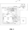
- a system 100 may include a printed circuit board (PCB) 102, a host 104, and a link 106, which is a communication link.
- PCB printed circuit board
- a flash memory 108 and an SOPC 110 may be located on PCB 102.
- SOPC 110 may include a control block 112, a sub-SOPC 114, and an interface 116.
- Sub-SOPC 114 may include a configurable core 118 and multiple chains 120 of input/output configuration shift registers (IOCSRs).
- Core 118 may include one or more logic blocks. Chain 120a or a portion of the chain 120a is an example of a logic block.
- Interface 116 may include a high-speed serial or parallel interface, such as a transceiver.
- interface 116 may include an IO pad.
- the IO pad may be a tristate buffer and may have an IO pin at its output.
- Interface 116 may include a block 122 that further may include one or more data registers 124.
- Block 122 may be a partially-configurable block.
- not all parameters of the partially-configurable block are pre-configured and may not be configured at a time of implementation of the partially-configurable block in a field of application. Examples of the field of application may include implementing SOPC 110 within a cell phone, within a radar system, or within a video game console.
- parameters of a logic block include a data width of the logic block, a speed of transmission of data from the logic block, and a speed of reception of data by the logic block.
- Host 104 may be a computer or a processor. Host 104 may communicate with interface 116 via link 106 by using a peripheral component interconnect express (PCI-e) standard, a PCI standard, a 2.5 gigabit standard, a 5 gigabit standard, or an 8 gigabit standard.
- PCI-e peripheral component interconnect express
- An example of link 106 may include a PCI-e link, a PCI link, a link that communicates using the 2.5 gigabit standard, the 5 gigabit standard, or the 8 gigabit standard.
- Control block 112 may be a controller and the controller may include a finite state machine and one or more registers. Flash memory 108 may be located off-chip. For example, flash memory 108 may be located on a substrate separate from a substrate of a chip in which SOPC 110 may be integrated.
- control block 112 may receive a first set of IOCSR configuration data from flash memory 108 via a link 126 either serially or in parallel and sends the first set of IOCSR configuration data to chains 120 to configure the IOCSRs of chains 120.
- control block 112 may receive via link 126, either serially or in parallel, a first set of interface configuration data from flash memory 108 and may store the first set of interface configuration data within the IOCSRs of one or more chains 120.
- IOCSRs of one or more chains 120 may shift the first set of interface configuration data from one IOCSR to another IOCSR in the one or more chains 120 to provide the first set of interface configuration data via a link 128 to interface 116 to configure the interface 116.
- interface 116 may establish communication via link 106 with host 104, may receive core configuration data from the host 104 via link 106 and may store the core configuration data in one or more data registers 124.
- Control block 112 may receive the core configuration data from one or more data registers 124 of interface 116 and may send the core configuration data to core 118 to configure the core 118.
- core 118 may be configured, the entire SOPC 110 may be configured.
- flash memory 108 instead of flash memory 108, another nonvolatile memory, such as a programmable read-only memory (PROM) may be used. In various alternative embodiments, flash memory 108 may not be located on PCB 102 and may be located on another PCB.
- PROM programmable read-only memory
- logic block 122 may be a fully-configurable block.
- a structure within the fully-configurable block and all parameters of the fully-configurable block can be configured at a time the fully-configurable block is implemented within the field.
- SOPC 110 may include any number or any type of layout of chains 120 other than that shown in Figure 1 .
- a system 200 may include a portion of chain 120a ( Figure 1 ) of IOCSRs.
- system 200 may include multiple flip flops 202 and 204, each of which may be an example of a portion of IOCSR of chain 120a ( Figure 1 ).
- System 200 may further include multiple AND gates 206 and 208.
- Flip flop 202 may receive a portion of the first set of interface configuration data from flash memory 108 and at a time a CSR enable signal 210 is asserted, may transfer the portion via a connection 212 to interface 116 ( Figure 1 ).
- flip flop 204 may receive a portion of the first set of interface configuration data from flash memory 108 and at a time CSR enable signal is asserted, may transfer the portion via a connection 214 to interface 116 ( Figure 1 ).
- One or more connections, such as connection 212 and 214, may form link 128 that may connect interface 116 with chain 120a ( Figure 1 ).
- flip flops 202 and 204 may not be able to send the first set of interface configuration data to interface 116.
- chain 120a, 120b, 120c, or 120d may include any number of flip flops and AND gates.
- chain 120b, 120c, or 120d may be used instead.
- a system 300 may include a PCB 302, link 106, and host 104.
- PCB 302 may include an SOPC 304 that further includes control block 112, interface 116, and a sub-SOPC 306.
- SOPC 304 may be a Field Programmable Gate Array (FPGA), an Application Specific Integrated Circuit (ASIC), or a custom ASIC.
- FPGA Field Programmable Gate Array
- ASIC Application Specific Integrated Circuit
- SOPC 304 may be a Stratix V ® FPGA available from Altera Corporation.
- Sub-SOPC 306 may include multiple chains 308 of IOCSRs and configurable core 118.
- System 300 may not include flash memory 108 ( Figure 1 ) or another non-volatile memory, such as a PROM, that sends configuration data to control block 112 to configure SOPC 304.
- Interface 116 may be connected to host 104 via link 106.
- a system 400 may include host 104, interface 116, control block 112, link 106, chain 308a of IOCSRs, and multiple multiplexers 402 and 404.
- Connection 212 output from AND gate 206 may be connected to an input 406 of multiplexer 402.
- Another input 408 of multiplexer 402 may be connected to either a first voltage source V1 or a second voltage source V2.
- the first voltage source V1 may be a positive direct current (DC) voltage source VCC and the second voltage source V2 may be a ground DC voltage source VSS.
- the first voltage source V1 may provide an alternating current (AC) and the second voltage source V2 may provide an alternating current.
- connection 214 output from AND gate 208 may be connected to an input 410 of multiplexer 404.
- Another input 412 of multiplexer 404 may be connected to either the voltage source V1 or the voltage source V2.
- Selection inputs 411 and 413 of multiplexers 402 and 404 may be connected to a user mode bit, which may be stored in a register of control block 112, and the usermode bit may be controlled by a value of the register, which may be controlled by the state machine of control block 112.
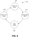
- FIG. 6 a state diagram 600 illustrating various states or "modes" that the SOPC 304 ( Figure 3 ) may be in is described.
- the SOPC 304 When the SOPC 304 is first powered on, or reset, the SOPC 304 begins in a power-up mode 602. Reference will be made to Figures 3 and 4 to aid in the discussion of the power-up mode 602.
- power In the power-up mode 602 ( Figure 6 ), power may be supplied to at least a portion of system 400 ( Figure 4 ), such as interface 116 and control block 112.
- the IOCSRs of multiple chains 308 ( Figure 3 ) may not be configured from the first set of IOCSR configuration data received from flash memory 108 ( Figure 1 ).
- control block 112 may control the user mode bit to be of a first value, such as zero or one.
- each multiplexer 402 and 404 may select an input power signal (inputs 408 and 412), which may be a signal received from the voltage source V1 or V2.
- Multiplexer 402 may output at its output 416 the input power signal received from the voltage source V1 or V2 and multiplexer 404 may output at its output 418 the input power signal received from the voltage source V1 or V2.
- input power signals output from outputs 416 and 418 may be the first set of interface configuration data used to configure interface 116.
- system 400 may include any number of flip flops, any number of multiplexers, and any number of AND gates.
- the system 400 may include as many multiplexers as required to provide configuration data used to configure interface 116.
- each multiplexer may receive a fixed voltage signal, e.g., VCC or VSS, or may receive a selectable voltage signal.
- the voltage signals received by the multiplexer may be any values used to configure interface 116.
- a configuration mode 604 ( Figure 6 ) may be entered into by SOPC 304 ( Figure 3 ).
- interface 116 may access the core configuration data and a second set of IOCSR configuration data from host 104 via link 106 ( Figure 3 ).
- core 118 may be configured with the core configuration data accessed by interface 116 from host 104 and chains 308 ( Figure 3 ) may be configured with the second set of IOCSR configuration data accessed by interface 116 from host 104.
- chains 308 ( Figure 3 ) may be configured with the second set of IOCSR configuration data accessed by interface 116 from host 104.
- a second set of interface configuration data may be stored in one or more IOCSRs of the chains 308.
- control block 112 may control each multiplexer 402 and 404 to continue to output the input power signal received from the voltage source V1 or V2.
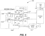
- Figure 5 depicts the system 400 configured in a "user mode".
- a user mode 606 ( Figure 6 ) may be entered into by the SOPC 304 ( Figure 3 ).
- control block 112 may control multiplexers 402 and 404 to output the second set of interface configuration data that is received from host 104 via interface 116 by chains 308 ( Figure 3 ).
- the second set of interface configuration data may be used to configure interface 116 during user mode 606.
- control block 112 may change a value of the user mode bit from the first value to a second value, such as 1, and upon receiving the selection of the second value, multiplexers 402 and 404 may output the second set of interface configuration data received by chains 308 from host 104 via link 106 and interface 116.
- CSR enable signal may be enabled, AND gate 206 may output a first portion of the second set of interface configuration data received from flip flop 202 and AND gate 208 may output the remaining portion of the second set of interface configuration data received from flip flop 204.
- Flip flop 202 may output, synchronous with a clock signal, to AND gate 206, the first portion received from an IOCSR of chain 308a.
- Flip flop 204 may output, synchronous with the clock signal, to AND gate 208, the second portion received from an IOCSR of chain 308a.
- AND gates 206 and 208 may output the first and second portions to interface 116.
- SOPC 304 ( Figure 3 ) may enter a power-down mode 608 ( Figure 6 ), which may occur as a result of a planned power-down of SOPC 304 or an unplanned power-down of SOPC 304, such as a result of a fault of a system that implements SOPC 304.
- the SOPC 304 may again configure itself beginning with power-up mode 602.
- system 300 may be provided for other SOPC functions during the user mode 606.
- System 300 may include flash memory 108 or another non-volatile memory but control block 112 may be restricted, during power-up mode 602 and configuration mode 604 ( Figure 6 ) from accessing configuration data from the flash memory 108 or the other non-volatile memory.
- SOPC 304 may be restricted from being configured by configuration data stored within flash memory 108 or the other non-volatile memory by using a switch (not shown) that is controlled by control block 112.
- control block 112 may open the switch to restrict SOPC 304 from being configured by configuration data stored within flash memory 108 or the other non-volatile memory.
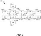
- a PLD 700 may include a two-dimensional array of programmable logic array blocks (LABs) 702 that are interconnected by a network of multiple column interconnects 710 and multiple row interconnects 712 of varying length and speed. Any of the LABs 702, e.g., LAB 702c, can perform one or more functions, such as, digital signal processing (DSP), addition, multiplication, subtraction, etc.
- the network of column interconnects 710 and row interconnects 712 may include multiple switching circuits (not shown) that can be configured.
- LABs 702 may include multiple logic elements (LEs) (not shown) and each LE may include one or more registers (not shown).
- the LEs of one LAB 702a may be coupled to LEs of another LAB 702b via one or more switching circuits (not shown).
- a set of input/output (I/O) elements 708 may be located around the periphery of PLD 700 to support numerous single-ended and differential IO standards.
- PLD 700 may further include a set of buffers (Bs) 714 that couple to LABs 702.
- the buffers 714 may be used to store data that is transferred between LABs 702.
- PLD 700 may function synchronous or asynchronous with one or more clock signals received via a clock tree (not shown).
- the clock tree may be overlaid on the PLD 700.
- the PLD 700 may be configured using a computer system.
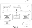
- a computer system 800 may include a processing unit 802, a memory device 804, a network interface 806, an input device 808, an output interface 810, and an output device 812.
- Network interface 806, output interface 810, memory device 804, and processing unit 802 may be located within a housing 814 of the computer system 800.
- Processing unit 802 may be a central processing unit (CPU), a microprocessor, a floating point coprocessor, a graphics coprocessor, a hardware controller, a microcontroller, a programmable logic device programmed for use as a controller, a network controller, or other processing unit.
- Memory device 804 may be a random access memory (RAM), a read-only memory (ROM), or a combination of RAM and ROM.
- RAM random access memory
- ROM read-only memory
- memory device 804 may include a non-transitory computer-readable medium, such as a floppy disk, a ZIPTM disk, a magnetic disk, a hard disk, a compact disc-ROM (CD-ROM), a recordable CD, a digital video disc (DVD), or a flash memory.
- Memory device 804 may store a program code for in accordance with embodiments of the present invention for execution by the processing unit 802.
- memory device 804 may store the program code for creating a design of SOPC 304, and configuring the SOPC 304 ( Figure 3 ), to name a few.
- Network interface 806 may be a modem or a network interface card (NIC) that allows processing unit 802 to communicate with a network 816, such as a wide area network (WAN) or a local area network (LAN).
- Processing unit 802 may be coupled via a wireless connection or a wired connection to network 816.
- Examples of the wireless connection include a connection using Wi-Fi protocol or a WiMax protocol.
- the Wi-Fi protocol may be an IEEE 802.11, IEEE 802.11a, IEEE 802.11b, IEEE 802.11g, or IEEE 802.11i protocol.
- Examples of input device 108 include a mouse, a display device, a keyboard, a stylus, a microphone, a keypad, etc.
- Output device 812 may be a liquid crystal display (LCD) device, a plasma display device, a light emitting diode (LED) display device, or a cathode ray tube (CRT) display device.
- Examples of output interface 810 include a video controller that drives output device 812 to display one or more images based on instructions received from processing unit 802.
- input device 808 and output device 812 may be integrated within the same device, such as a display device having a touch screen.
- Processing unit 102 accesses the program code stored on memory device 804 or stored on a remote memory device (not shown), similar to memory device 804, via network 816. The processor unit 102 executes the program code stored therein in order to implement the methods in accordance with various embodiments of the present invention.
- Processing unit 802, memory device 804, network interface 806, input device 808, output interface 810, and output device 1812 communicate with each other via a bus 818.
- system 800 may not include input device 808 and/or network interface 806.
- network interface 806, output interface 810, memory device 804, and processing unit 802 may be located outside the structure of housing 814.
- multiple memory devices may be used instead of memory device 804.
- multiple processing units may be used instead of processing unit 802.
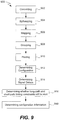
- a method 900 for creating a design of an SOPC in accordance with one embodiment is shown.
- the created design may be subsequently used to generate configuration information for configuring the PLD 700.
- Processing unit 802 ( Figure 8 ) may access the program code, stored within memory device 804, for execution thereof in order to implement the method 900 in accordance with one embodiment.
- Processing unit 802 may execute the program code for the method 900 to convert a user design in a given format, e.g., Hardware Description Language (HDL), into the configuration information.
- the PLD 700 is configured based on the configuration information to implement the user design.
- a user design is converted into a register transfer layer (RTL) design of PLD 700.
- the RTL design may include a flow of signals between registers and logical operations that may be performed on the signals.
- the RTL design is synthesized into a set of logic gates. This set of logic gates may provide a synthesized design of PLD 700.
- the set of logic gates is mapped into a set of atoms.
- An atom is generally referred to irreducible constituents of a user design.
- the atoms may correspond to groups of logic gates and other components of the user design matching the capabilities of the LEs or other functional blocks of PLD 700.
- the user design may be converted into any number of different sets of atoms, depending upon the underlying hardware of PLD 700 used to implement the user design.
- related atoms are grouped together to form clusters.
- the clusters of atoms are placed on multiple locations on PLD 700.
- configuration of the switching circuits of PLD 700 used to couple the atoms implementing the user design is determined.
- multiple signal delays, e.g., data delays, for the sets of atoms and their associated connections in the switching circuits are determined by using a timing model of the PLD 700.
- the configuration information is determined.
- the configuration information may include a configuration of each LE and the switching circuits used to couple the LEs.
- the configuration information is written in to a configuration file capable of being stored in the memory device 804 ( Figure 8 ) for access thereof.
- the configuration file may be accessed by the processing unit 802 to configure the PLD 700.
- Example 1 provides a system comprising: a first voltage input; a second voltage input; and a system on a programmable chip (SOPC) including a core and an interface, wherein during a first mode of the SOPC, the interface is configured via the first voltage input or the second voltage input.
- SOPC system on a programmable chip
- Additional Example 2 relates to the system of Additional Example 1, wherein during the first mode, the interface is restricted from being configured based on a first set of configuration data stored in an external non-volatile memory, wherein the first voltage input includes a direct current voltage input, and wherein the second voltage input includes a direct current voltage input.
- Additional Example 3 relates to the system of Additional Example 1 or 2, further comprising: a configuration shift register; and a multiplexer configured to multiplex between an output of the first voltage input or an output of the configuration shift register based on a value of a user-mode bit.
- Additional Example 4 relates to the system of one of the preceding Additional Examples, further comprising: a plurality of configuration shift registers, wherein the interface is configured to communicate with a host via a link during the first mode, and further wherein during a second mode, the SOPC receives a second set of configuration data from the host via the interface and wherein the SOPC configures the plurality of configuration shift registers to store the second set of configuration data.
- Additional Example 5 relates to the system of Additional Example 4, wherein during the second mode, the interface is configured via the first or second voltage input and the core is configured.
- Additional Example 6 relates to the system of Additional Example 5, wherein during a third mode, the interface is configured by the second set of configuration data stored in the plurality of configuration shift registers in response to a configuration of the core and the configuration of the plurality of the configuration shift registers.
- Additional Example 7 relates to the system of Additional Example 6, wherein during the third mode, the interface is restricted from being configured by the first set of configuration data.
- Additional Example 8 relates to the system of one of the preceding Additional Examples, further comprising a link connecting the interface to a host, wherein the interface is configured to transfer data to the host at a rate of gigabits per second.
- Additional Example 9 relates to the system of one of the preceding Additional Examples, wherein the SOPC includes a field programmable gate array (FPGA) or an Application Specific Integrated Circuit (ASIC).
- FPGA field programmable gate array
- ASIC Application Specific Integrated Circuit
- Additional Example 10 provides a method comprising configuring, during a first mode, an interface of a system on a programmable chip (SOPC) via a first voltage input or a second voltage input.
- SOPC system on a programmable chip
- Additional Example 11 relates to the method of Additional Example 10, further comprising restricting, during the first mode, the interface from being configured based on configuration data stored in a flash memory or a programmable read only memory.
- Additional Example 12 relates to the method of Additional Example 10 or 11, further comprising multiplexing between an output of the first voltage input or an output of a configuration shift register based on a value of a user-mode bit.
- Additional Example 13 relates to the method of one of the Additional Examples 10 to 12, further comprising: storing a plurality of configuration bits in a plurality of configuration shift registers of the SOPC, wherein said storing the plurality of configuration bits is performed by configuring, during a second mode, the plurality of configuration shift registers of the SOPC based on configuration data received from a host; configuring, during the second mode, a core of the SOPC, wherein said configuring the core and the plurality of configuration shift registers is performed in response to said configuring the interface during the first mode.
- Additional Example 14 relates to the method of Additional Example 13, further comprising configuring, during a third mode, the interface by the plurality of configuration bits stored in the plurality of configuration shift registers in response to the configuration of the core and the configuration of the plurality of the configuration shift registers.
- Additional Example 15 relates to the method of Additional Example 14, further comprising restricting, during the third mode, the interface from being configured by the first and second voltage sources.
- Additional Example 16 relates to the method of one of the Additional Examples 10 to 15, further comprising transferring data between the interface and a host at a rate of gigabits per second by coupling a link between the interface and the host.
- Additional Example 17 relates to the method of one of the Additional Examples 10 to 16, wherein the SOPC includes a field programmable gate array (FPGA) or an Application Specific Integrated Circuit (ASIC).
- FPGA field programmable gate array
- ASIC Application Specific Integrated Circuit
Abstract
Description
- This application claims benefit
U.S. Patent Application No. 13/103,878, titled "SYSTEMS AND METHODS FOR CONFIGURING AN SOPC WITHOUT A NEED TO USE AN EXTERNAL MEMORY", naming HOOI, et al. as inventors, filed 9 May 2011 - The present disclosure generally relates to systems and techniques for configuring a system on a programmable chip (SOPC) without a need to use an external memory.
- A system on a programmable chip (SOPC) includes one or more integrated circuits that may be programmed to perform one or more logic functions. One type of SOPC may be implemented using a Field Programmable Gate Array (FPGA). The FPGA may include an array of logic blocks. These logic blocks can include, for example, input/output Blocks, Random Access Memory Blocks (BRAMs), multipliers, Digital Signal Processing blocks (DSPs), processors, clock managers, Delay Lock Loops (DLLs), Multi-Gigabit Transceivers (MGTs), and so forth.
- Each logic block typically includes both programmable interconnect and programmable logic. The programmable interconnect typically includes a large number of interconnect lines of varying lengths interconnected by Programmable Interconnect Points (PIPs). The programmable interconnect and the programmable logic are typically programmed by loading a stream of configuration data into internal configuration memory cells that define how the logic blocks are configured. The configuration data may be read from a configuration memory, such as an external programmable read-only memory (PROM) or external Flash memory. The collective states of the individual memory cells then determine the function of the FPGA.
- As FPGAs grow in size and capability, the amount of configuration memory used to configure the logic blocks also increases. This configuration memory may be expensive and may also require additional space on a board on which the SOPC is implemented. For example, the Flash memory may be costly and also may consume a large amount of board area.
- Systems and techniques for configuration of a system on a programmable chip (SOPC) may reduce a need for flash memory or any such non-volatile memory at a time the SOPC is being configured. The systems and techniques reduce a need for the non-volatile memory by providing one or more voltage sources. Rather than obtaining configuration data from the non-volatile memory, the one or more voltage sources provide the configuration data. As a result, cost of designing and implementing the flash memory or the other non-volatile memory may be reduced and more board space on a printed circuit board (PCB) may be available for other devices.
- In one aspect, a system is described. The system may include a first voltage input, a second voltage input, and the SOPC. The SOPC may include a core and an interface. During power-up of the SOPC, the interface may be configured via the first voltage input or the second voltage input. Accordingly, the configuration via the first or second voltage input during the power-up may reduce a need for the flash memory or any such non-volatile memory at a time the SOPC is being configured.
- According to a further aspect the invention relates to a system comprising a host; a system on a programmable chip (SOPC) including a core and an interface, wherein the interface is coupled to the host via a link; a first voltage source; and a second voltage source, wherein during a first mode, the interface is configured by apply voltage from the first voltage source or the second voltage source.
- Preferably in such a system the SOPC includes a field programmable gate array (FPGA) or an Application Specific Integrated Circuit (ASIC), wherein the host includes a computer, wherein the first and second voltage sources are located on a printed circuit board, and wherein the interface is located on the printed circuit board.
- Further preferably in such a system the SOPC is configured using configuration information from the host.
- The systems and techniques may best be understood by reference to the following description taken in conjunction with the accompanying drawings, which illustrate various embodiments of the present systems and techniques. In the drawings, structural elements having the same or similar functions are denoted by like reference numerals.
-
Figure 1 shows an exemplary system on a programmable chip (SOPC) that is configured using a Flash memory. -
Figure 2 shows an exemplary portion of the SOPC to illustrate configuration of an interface of the system. -
Figure 3 shows an exemplary SOPC that is configured without using an external memory. -
Figure 4 shows an exemplary portion of the system ofFigure 3 to illustrate configuration of the system ofFigure 3 during a power-up mode and a configuration mode. -
Figure 5 shows the exemplary portion of the system ofFigure 3 to illustrate configuration of the system ofFigure 3 during a user mode. -
Figure 6 shows an exemplary technique for configuring the SOPC ofFigure 3 during the various modes. -
Figure 7 is shows an exemplary programmable logic device (PLD), which is used to implement the SOPC ofFigure 3 . -
Figure 8 shows an exemplary computer system for designing and generating configuration information used to configure the SOPC ofFigure 3 . -
Figure 9 shows an exemplary compilation technique executed by the computer system to generate the configuration information - It is noted that in the drawings, structural elements having the same or similar functions are denoted by like reference numerals. Referring now to
Figure 1 , asystem 100 may include a printed circuit board (PCB) 102, ahost 104, and alink 106, which is a communication link. - A
flash memory 108 and an SOPC 110 may be located on PCB 102. SOPC 110 may include acontrol block 112, asub-SOPC 114, and aninterface 116.Sub-SOPC 114 may include aconfigurable core 118 and multiple chains 120 of input/output configuration shift registers (IOCSRs).Core 118 may include one or more logic blocks.Chain 120a or a portion of thechain 120a is an example of a logic block.Interface 116 may include a high-speed serial or parallel interface, such as a transceiver. As another example,interface 116 may include an IO pad. The IO pad may be a tristate buffer and may have an IO pin at its output. -
Interface 116 may include ablock 122 that further may include one ormore data registers 124.Block 122 may be a partially-configurable block. In various embodiments, not all parameters of the partially-configurable block are pre-configured and may not be configured at a time of implementation of the partially-configurable block in a field of application. Examples of the field of application may include implementing SOPC 110 within a cell phone, within a radar system, or within a video game console. Examples of parameters of a logic block include a data width of the logic block, a speed of transmission of data from the logic block, and a speed of reception of data by the logic block. -
Host 104 may be a computer or a processor.Host 104 may communicate withinterface 116 vialink 106 by using a peripheral component interconnect express (PCI-e) standard, a PCI standard, a 2.5 gigabit standard, a 5 gigabit standard, or an 8 gigabit standard. An example oflink 106 may include a PCI-e link, a PCI link, a link that communicates using the 2.5 gigabit standard, the 5 gigabit standard, or the 8 gigabit standard.Control block 112 may be a controller and the controller may include a finite state machine and one or more registers.Flash memory 108 may be located off-chip. For example,flash memory 108 may be located on a substrate separate from a substrate of a chip in which SOPC 110 may be integrated. - In various embodiments, during power-up of SOPC 110,
control block 112 may receive a first set of IOCSR configuration data fromflash memory 108 via alink 126 either serially or in parallel and sends the first set of IOCSR configuration data to chains 120 to configure the IOCSRs of chains 120. Upon configuring the IOCSR with the first set of IOCSR configuration data,control block 112 may receive vialink 126, either serially or in parallel, a first set of interface configuration data fromflash memory 108 and may store the first set of interface configuration data within the IOCSRs of one or more chains 120. IOCSRs of one or more chains 120 may shift the first set of interface configuration data from one IOCSR to another IOCSR in the one or more chains 120 to provide the first set of interface configuration data via alink 128 to interface 116 to configure theinterface 116. - In various embodiments, upon configuration of
interface 116,interface 116 may establish communication vialink 106 withhost 104, may receive core configuration data from thehost 104 vialink 106 and may store the core configuration data in one or more data registers 124.Control block 112 may receive the core configuration data from one ormore data registers 124 ofinterface 116 and may send the core configuration data tocore 118 to configure thecore 118. At atime core 118 may be configured, theentire SOPC 110 may be configured. - In various alternative embodiments, instead of
flash memory 108, another nonvolatile memory, such as a programmable read-only memory (PROM) may be used. In various alternative embodiments,flash memory 108 may not be located onPCB 102 and may be located on another PCB. - In various embodiments,
logic block 122 may be a fully-configurable block. A structure within the fully-configurable block and all parameters of the fully-configurable block can be configured at a time the fully-configurable block is implemented within the field. Moreover, in various embodiments,SOPC 110 may include any number or any type of layout of chains 120 other than that shown inFigure 1 . - With reference to
Figure 2 , asystem 200 may include a portion ofchain 120a (Figure 1 ) of IOCSRs. In some embodiments,system 200 may includemultiple flip flops chain 120a (Figure 1 ).System 200 may further include multiple ANDgates -
Flip flop 202 may receive a portion of the first set of interface configuration data fromflash memory 108 and at a time aCSR enable signal 210 is asserted, may transfer the portion via aconnection 212 to interface 116 (Figure 1 ). Similarly,flip flop 204 may receive a portion of the first set of interface configuration data fromflash memory 108 and at a time CSR enable signal is asserted, may transfer the portion via aconnection 214 to interface 116 (Figure 1 ). One or more connections, such asconnection interface 116 withchain 120a (Figure 1 ). At a time CSR enablesignal 210 is not asserted, flipflops - It is noted that although two flip-flops and two AND gates are shown in
Figure 2 , in various embodiments,chain chain 120a, in some embodiments,chain - Referring to
Figure 3 , asystem 300 may include aPCB 302, link 106, andhost 104.PCB 302 may include anSOPC 304 that further includescontrol block 112,interface 116, and asub-SOPC 306.SOPC 304 may be a Field Programmable Gate Array (FPGA), an Application Specific Integrated Circuit (ASIC), or a custom ASIC. For example,SOPC 304 may be a Stratix V® FPGA available from Altera Corporation.Sub-SOPC 306 may include multiple chains 308 of IOCSRs andconfigurable core 118.System 300 may not include flash memory 108 (Figure 1 ) or another non-volatile memory, such as a PROM, that sends configuration data to control block 112 to configureSOPC 304.Interface 116 may be connected to host 104 vialink 106. - With reference to
Figure 4 , in various embodiments, asystem 400 may includehost 104,interface 116,control block 112, link 106,chain 308a of IOCSRs, andmultiple multiplexers Connection 212 output from ANDgate 206 may be connected to aninput 406 ofmultiplexer 402. Anotherinput 408 ofmultiplexer 402 may be connected to either a first voltage source V1 or a second voltage source V2. As an example, the first voltage source V1 may be a positive direct current (DC) voltage source VCC and the second voltage source V2 may be a ground DC voltage source VSS. As another example, the first voltage source V1 may provide an alternating current (AC) and the second voltage source V2 may provide an alternating current. Similarly,connection 214 output from ANDgate 208 may be connected to aninput 410 ofmultiplexer 404. Anotherinput 412 ofmultiplexer 404 may be connected to either the voltage source V1 or the voltage source V2.Selection inputs multiplexers control block 112, and the usermode bit may be controlled by a value of the register, which may be controlled by the state machine ofcontrol block 112. - Referring to
Figure 6 , a state diagram 600 illustrating various states or "modes" that the SOPC 304 (Figure 3 ) may be in is described. When theSOPC 304 is first powered on, or reset, theSOPC 304 begins in a power-upmode 602. Reference will be made toFigures 3 and4 to aid in the discussion of the power-upmode 602. In the power-up mode 602 (Figure 6 ), power may be supplied to at least a portion of system 400 (Figure 4 ), such asinterface 116 andcontrol block 112. Unlike insystem 100, during power-upmode 602, the IOCSRs of multiple chains 308 (Figure 3 ) may not be configured from the first set of IOCSR configuration data received from flash memory 108 (Figure 1 ). Rather, during power-upmode 602, control block 112 may control the user mode bit to be of a first value, such as zero or one. At a time the user mode bit has the first value, eachmultiplexer inputs 408 and 412), which may be a signal received from the voltage source V1 or V2.Multiplexer 402 may output at itsoutput 416 the input power signal received from the voltage source V1 or V2 andmultiplexer 404 may output at itsoutput 418 the input power signal received from the voltage source V1 or V2. During power-upmode 602, input power signals output fromoutputs interface 116. - Although two flip-flops, two AND gates, and two multiplexers are shown in
Figure 4 , in various embodiments,system 400 may include any number of flip flops, any number of multiplexers, and any number of AND gates. Thesystem 400 may include as many multiplexers as required to provide configuration data used to configureinterface 116. Furthermore, each multiplexer may receive a fixed voltage signal, e.g., VCC or VSS, or may receive a selectable voltage signal. The voltage signals received by the multiplexer may be any values used to configureinterface 116. - Referring back to
Figure 6 , upon configuration ofinterface 116, a configuration mode 604 (Figure 6 ) may be entered into by SOPC 304 (Figure 3 ). Duringconfiguration mode 604,interface 116 may access the core configuration data and a second set of IOCSR configuration data fromhost 104 via link 106 (Figure 3 ). For example,core 118 may be configured with the core configuration data accessed byinterface 116 fromhost 104 and chains 308 (Figure 3 ) may be configured with the second set of IOCSR configuration data accessed byinterface 116 fromhost 104. While configuring chains 308 with the second set of IOCSR configuration data, a second set of interface configuration data may be stored in one or more IOCSRs of the chains 308. As in the power-up mode, control block 112 may control eachmultiplexer -
Figure 5 depicts thesystem 400 configured in a "user mode". Upon completion of configuration ofcore 118 and chains 308 ofSOPC 304 duringconfiguration mode 604, a user mode 606 (Figure 6 ) may be entered into by the SOPC 304 (Figure 3 ). Referring toFigure 6 , duringuser mode 606, control block 112 may controlmultiplexers host 104 viainterface 116 by chains 308 (Figure 3 ). The second set of interface configuration data may be used to configureinterface 116 duringuser mode 606. In some embodiments, control block 112 may change a value of the user mode bit from the first value to a second value, such as 1, and upon receiving the selection of the second value,multiplexers host 104 vialink 106 andinterface 116. Moreover, duringuser mode 606, CSR enable signal may be enabled, ANDgate 206 may output a first portion of the second set of interface configuration data received fromflip flop 202 and ANDgate 208 may output the remaining portion of the second set of interface configuration data received fromflip flop 204.Flip flop 202 may output, synchronous with a clock signal, to ANDgate 206, the first portion received from an IOCSR ofchain 308a.Flip flop 204 may output, synchronous with the clock signal, to ANDgate 208, the second portion received from an IOCSR ofchain 308a. ANDgates - In some embodiments, SOPC 304 (
Figure 3 ) may enter a power-down mode 608 (Figure 6 ), which may occur as a result of a planned power-down ofSOPC 304 or an unplanned power-down ofSOPC 304, such as a result of a fault of a system that implementsSOPC 304. When exiting power-down mode 608, theSOPC 304 may again configure itself beginning with power-upmode 602. - In various embodiments, while
system 300 has been depicted as being configured without the use of non-volatile memory, such memory, e.g. Flash memory 108 (Figure 1 ), may be provided for other SOPC functions during theuser mode 606.System 300 may includeflash memory 108 or another non-volatile memory but control block 112 may be restricted, during power-upmode 602 and configuration mode 604 (Figure 6 ) from accessing configuration data from theflash memory 108 or the other non-volatile memory. In these various embodiments,SOPC 304 may be restricted from being configured by configuration data stored withinflash memory 108 or the other non-volatile memory by using a switch (not shown) that is controlled bycontrol block 112. For example, during power-upmode 602 andconfiguration mode 604, control block 112 may open the switch to restrictSOPC 304 from being configured by configuration data stored withinflash memory 108 or the other non-volatile memory. - The
SOPC 304 can be implemented using a PLD. With reference toFigure 7 , aPLD 700 may include a two-dimensional array of programmable logic array blocks (LABs) 702 that are interconnected by a network of multiple column interconnects 710 and multiple row interconnects 712 of varying length and speed. Any of the LABs 702, e.g.,LAB 702c, can perform one or more functions, such as, digital signal processing (DSP), addition, multiplication, subtraction, etc. The network of column interconnects 710 and row interconnects 712 may include multiple switching circuits (not shown) that can be configured. LABs 702 may include multiple logic elements (LEs) (not shown) and each LE may include one or more registers (not shown). The LEs of oneLAB 702a may be coupled to LEs of anotherLAB 702b via one or more switching circuits (not shown). A set of input/output (I/O) elements 708 may be located around the periphery ofPLD 700 to support numerous single-ended and differential IO standards.PLD 700 may further include a set of buffers (Bs) 714 that couple to LABs 702. The buffers 714 may be used to store data that is transferred between LABs 702.PLD 700 may function synchronous or asynchronous with one or more clock signals received via a clock tree (not shown). The clock tree may be overlaid on thePLD 700. - The
PLD 700 may be configured using a computer system. Referring toFigure 8 , acomputer system 800 may include aprocessing unit 802, amemory device 804, anetwork interface 806, aninput device 808, anoutput interface 810, and anoutput device 812.Network interface 806,output interface 810,memory device 804, andprocessing unit 802 may be located within a housing 814 of thecomputer system 800. -
Processing unit 802 may be a central processing unit (CPU), a microprocessor, a floating point coprocessor, a graphics coprocessor, a hardware controller, a microcontroller, a programmable logic device programmed for use as a controller, a network controller, or other processing unit.Memory device 804 may be a random access memory (RAM), a read-only memory (ROM), or a combination of RAM and ROM. For example,memory device 804 may include a non-transitory computer-readable medium, such as a floppy disk, a ZIP™ disk, a magnetic disk, a hard disk, a compact disc-ROM (CD-ROM), a recordable CD, a digital video disc (DVD), or a flash memory.Memory device 804 may store a program code for in accordance with embodiments of the present invention for execution by theprocessing unit 802. For example,memory device 804 may store the program code for creating a design ofSOPC 304, and configuring the SOPC 304 (Figure 3 ), to name a few. -
Network interface 806 may be a modem or a network interface card (NIC) that allows processingunit 802 to communicate with anetwork 816, such as a wide area network (WAN) or a local area network (LAN).Processing unit 802 may be coupled via a wireless connection or a wired connection tonetwork 816. Examples of the wireless connection include a connection using Wi-Fi protocol or a WiMax protocol. The Wi-Fi protocol may be an IEEE 802.11, IEEE 802.11a, IEEE 802.11b, IEEE 802.11g, or IEEE 802.11i protocol. Examples ofinput device 108 include a mouse, a display device, a keyboard, a stylus, a microphone, a keypad, etc. -
Output device 812 may be a liquid crystal display (LCD) device, a plasma display device, a light emitting diode (LED) display device, or a cathode ray tube (CRT) display device. Examples ofoutput interface 810 include a video controller that drivesoutput device 812 to display one or more images based on instructions received from processingunit 802. In various embodiments,input device 808 andoutput device 812 may be integrated within the same device, such as a display device having a touch screen.Processing unit 102 accesses the program code stored onmemory device 804 or stored on a remote memory device (not shown), similar tomemory device 804, vianetwork 816. Theprocessor unit 102 executes the program code stored therein in order to implement the methods in accordance with various embodiments of the present invention.Processing unit 802,memory device 804,network interface 806,input device 808,output interface 810, and output device 1812 communicate with each other via abus 818. - In various embodiments,
system 800 may not includeinput device 808 and/ornetwork interface 806. In some embodiments,network interface 806,output interface 810,memory device 804, andprocessing unit 802 may be located outside the structure of housing 814. - In some embodiments, multiple memory devices may be used instead of
memory device 804. Moreover, in one embodiment, multiple processing units may be used instead of processingunit 802. - With reference to
Figure 9 , amethod 900 for creating a design of an SOPC in accordance with one embodiment is shown. The created design may be subsequently used to generate configuration information for configuring thePLD 700. Processing unit 802 (Figure 8 ) may access the program code, stored withinmemory device 804, for execution thereof in order to implement themethod 900 in accordance with one embodiment. -
Processing unit 802 may execute the program code for themethod 900 to convert a user design in a given format, e.g., Hardware Description Language (HDL), into the configuration information. ThePLD 700 is configured based on the configuration information to implement the user design. - At
operation 902, a user design is converted into a register transfer layer (RTL) design ofPLD 700. As an example, the RTL design may include a flow of signals between registers and logical operations that may be performed on the signals. Atoperation 904, the RTL design is synthesized into a set of logic gates. This set of logic gates may provide a synthesized design ofPLD 700. Atoperation 906, the set of logic gates is mapped into a set of atoms. An atom is generally referred to irreducible constituents of a user design. The atoms may correspond to groups of logic gates and other components of the user design matching the capabilities of the LEs or other functional blocks ofPLD 700. The user design may be converted into any number of different sets of atoms, depending upon the underlying hardware ofPLD 700 used to implement the user design. - At
operation 908, related atoms are grouped together to form clusters. Atoperation 910, the clusters of atoms are placed on multiple locations onPLD 700. Atoperation 912, configuration of the switching circuits ofPLD 700 used to couple the atoms implementing the user design is determined. Atoperation 914, multiple signal delays, e.g., data delays, for the sets of atoms and their associated connections in the switching circuits are determined by using a timing model of thePLD 700. Atoperation 916, it is determined whether the implementation of the user design inPLD 700 will meet multiple long-path and short-path timing constraints. It is appreciated that in one embodiment, the timing constraints may be user specified via input device 808 (Figure 8 ). - At
operation 918, the configuration information is determined. The configuration information may include a configuration of each LE and the switching circuits used to couple the LEs. Atoperation 918, the configuration information is written in to a configuration file capable of being stored in the memory device 804 (Figure 8 ) for access thereof. For example, the configuration file may be accessed by theprocessing unit 802 to configure thePLD 700. - Technical effects of the herein described systems and techniques for configuration of an SOPC may include eliminating a need for flash memory 108 (
Figure 1 ) at a time SOPC 304 (Figure 3 ) is being configured. As a result, cost of designing and implementing flash memory 108 (Figure 1 ) may be reduced and more board space on PCB 102 (Figure 1 ) may be available or a smaller PCB 302 (Figure 3 ) than PCB 102 (Figure 1 ) can be used. Moreover, power for operating flash memory 108 (Figure 1 ) may be saved. For example, in case a separate power supply may be used to operate flash memory 108 (Figure 1 ) than a power supply used to operate SOPC 110 (Figure 1 ), the systems and techniques may reduce the need for the separate power supply. The systems and techniques, described herein, may save the cost of the separate power supply. - Additional Example 1 provides a system comprising: a first voltage input; a second voltage input; and a system on a programmable chip (SOPC) including a core and an interface, wherein during a first mode of the SOPC, the interface is configured via the first voltage input or the second voltage input.
- Additional Example 2 relates to the system of Additional Example 1, wherein during the first mode, the interface is restricted from being configured based on a first set of configuration data stored in an external non-volatile memory, wherein the first voltage input includes a direct current voltage input, and wherein the second voltage input includes a direct current voltage input.
- Additional Example 3 relates to the system of Additional Example 1 or 2, further comprising: a configuration shift register; and a multiplexer configured to multiplex between an output of the first voltage input or an output of the configuration shift register based on a value of a user-mode bit.
- Additional Example 4 relates to the system of one of the preceding Additional Examples, further comprising: a plurality of configuration shift registers, wherein the interface is configured to communicate with a host via a link during the first mode, and further wherein during a second mode, the SOPC receives a second set of configuration data from the host via the interface and wherein the SOPC configures the plurality of configuration shift registers to store the second set of configuration data.
- Additional Example 5 relates to the system of Additional Example 4, wherein during the second mode, the interface is configured via the first or second voltage input and the core is configured.
- Additional Example 6 relates to the system of Additional Example 5, wherein during a third mode, the interface is configured by the second set of configuration data stored in the plurality of configuration shift registers in response to a configuration of the core and the configuration of the plurality of the configuration shift registers.
- Additional Example 7 relates to the system of Additional Example 6, wherein during the third mode, the interface is restricted from being configured by the first set of configuration data.
- Additional Example 8 relates to the system of one of the preceding Additional Examples, further comprising a link connecting the interface to a host, wherein the interface is configured to transfer data to the host at a rate of gigabits per second.
- Additional Example 9 relates to the system of one of the preceding Additional Examples, wherein the SOPC includes a field programmable gate array (FPGA) or an Application Specific Integrated Circuit (ASIC).
- Additional Example 10 provides a method comprising configuring, during a first mode, an interface of a system on a programmable chip (SOPC) via a first voltage input or a second voltage input.
- Additional Example 11 relates to the method of Additional Example 10, further comprising restricting, during the first mode, the interface from being configured based on configuration data stored in a flash memory or a programmable read only memory.
- Additional Example 12 relates to the method of Additional Example 10 or 11, further comprising multiplexing between an output of the first voltage input or an output of a configuration shift register based on a value of a user-mode bit.
- Additional Example 13 relates to the method of one of the Additional Examples 10 to 12, further comprising: storing a plurality of configuration bits in a plurality of configuration shift registers of the SOPC, wherein said storing the plurality of configuration bits is performed by configuring, during a second mode, the plurality of configuration shift registers of the SOPC based on configuration data received from a host; configuring, during the second mode, a core of the SOPC, wherein said configuring the core and the plurality of configuration shift registers is performed in response to said configuring the interface during the first mode.
- Additional Example 14 relates to the method of Additional Example 13, further comprising configuring, during a third mode, the interface by the plurality of configuration bits stored in the plurality of configuration shift registers in response to the configuration of the core and the configuration of the plurality of the configuration shift registers.
- Additional Example 15 relates to the method of Additional Example 14, further comprising restricting, during the third mode, the interface from being configured by the first and second voltage sources.
- Additional Example 16 relates to the method of one of the Additional Examples 10 to 15, further comprising transferring data between the interface and a host at a rate of gigabits per second by coupling a link between the interface and the host.
- Additional Example 17 relates to the method of one of the Additional Examples 10 to 16, wherein the SOPC includes a field programmable gate array (FPGA) or an Application Specific Integrated Circuit (ASIC).
- Although the foregoing systems and techniques have been described in detail by way of illustration and example for purposes of clarity and understanding, it will be recognized that the above described systems and techniques may be embodied in numerous other variations and embodiments without departing from the spirit or essential characteristics of the systems and techniques. Some changes and modifications may be practiced, and it is understood that the systems and techniques are not to be limited by the foregoing details, but rather is to be defined by the scope of the appended claims.
Claims (15)
- An integrated circuit device comprising:a FPGA fabric; anda communication interface;wherein the integrated circuit device is adapted to:during a first initialization stage, configure the communication interface to enable communication via the communication interface; andduring a second initialization stage, initially configure at least a portion of the FPGA fabric using data received via the communication interface.
- The integrated circuit of claim 1, wherein the integrated circuit is adapted to, during a third initialization stage, in response to the integrated circuit initially configuring at least the portion of the FPGA fabric, configure the communication interface to operate in a user mode.
- The integrated circuit of claim 1, wherein the integrated circuit is adapted to, during the first initialization stage, configure the communication interface using interface configuration data received from a programmable read-only memory (PROM).
- The integrated circuit of claim 1, wherein the integrated circuit is adapted to configure the communication interface to enable communication using a peripheral component interconnect express (PCI-e) standard.
- The integrated circuit of claim 1, wherein the portion of the FPGA fabric does not include the communication interface.
- The integrated circuit of claim 1, wherein the data is received from a data source external to the integrated circuit.
- A system comprising an integrated circuit of one of claims 1 to 6.
- An integrated circuit comprising:field programmable gate array (FPGA) fabric; anda communication interface,wherein:before a first initialization stage, the communication interface is not configured to enable the communication interface to receive data via a first communication protocol;during the first initialization stage, the communication interface is adapted to become configured to enable the communication interface to receive data via the first communication protocol; andduring a second initialization stage, the communication interface is adapted to receive data via the first communication protocol to enable the integrated circuit device to initially configure at least a portion of the FPGA fabric.
- The integrated circuit of claim 8, wherein, during a third initialization stage, in response to the integrated circuit initially configuring at least the portion of the FPGA fabric, the communication interface is adapted to become configured to operate in a user mode.
- The integrated circuit of claim 8, wherein, during the first initialization stage, the integrated circuit is adapted to configure the communication interface using interface configuration data received from a programmable read-only memory (PROM).
- One or more machine-readable media comprising instructions configured to cause a control block of an integrated circuit to:during a first initialization stage, configure a communication interface of the integrated circuit, wherein the configuration of the communication interface during the first initialization stage enables communication via the communication interface; andduring a second initialization stage, initially configure at least a portion of field programmable gate array (FPGA) fabric using data received via the communication interface.
- The one or more machine-readable media of claim 11, comprising instructions configured to cause the control block to, during a third initialization stage, in response to the control block initially configuring at least the portion of the FPGA fabric, configure the communication interface to operate in a user mode.
- The one or more machine-readable media of claim 11, wherein, during the first initialization stage, the control block configures the communication interface using interface configuration data received from a programmable read-only memory (PROM).
- The one or more machine-readable media of claim 13, wherein the control block configures the communication interface to enable communication using a peripheral component interconnect express (PCI-e) standard.
- A method comprising:during a first initialization stage, configuring, via a control block of an integrated circuit, a communication interface of the integrated circuit, wherein the configuration of the communication interface during the first initialization stage enables communication via the communication interface; andduring a second initialization stage, initially configuring, via the control block, at least a portion of field programmable gate array (FPGA) fabric using data received via the communication interface.
Applications Claiming Priority (2)
| Application Number | Priority Date | Filing Date | Title |
|---|---|---|---|
| US13/103,878 US9543956B2 (en) | 2011-05-09 | 2011-05-09 | Systems and methods for configuring an SOPC without a need to use an external memory |
| EP12167132.5A EP2523349B1 (en) | 2011-05-09 | 2012-05-08 | Systems and methods for configuring an SOPC without a need to use an external memory |
Related Parent Applications (2)
| Application Number | Title | Priority Date | Filing Date |
|---|---|---|---|
| EP12167132.5A Division EP2523349B1 (en) | 2011-05-09 | 2012-05-08 | Systems and methods for configuring an SOPC without a need to use an external memory |
| EP12167132.5A Division-Into EP2523349B1 (en) | 2011-05-09 | 2012-05-08 | Systems and methods for configuring an SOPC without a need to use an external memory |
Publications (2)
| Publication Number | Publication Date |
|---|---|
| EP3223430A1 true EP3223430A1 (en) | 2017-09-27 |
| EP3223430B1 EP3223430B1 (en) | 2020-06-24 |
Family
ID=46085811
Family Applications (2)
| Application Number | Title | Priority Date | Filing Date |
|---|---|---|---|
| EP17169092.8A Active EP3223430B1 (en) | 2011-05-09 | 2012-05-08 | Systems and methods for configuring an sopc without a need to use an external memory |
| EP12167132.5A Active EP2523349B1 (en) | 2011-05-09 | 2012-05-08 | Systems and methods for configuring an SOPC without a need to use an external memory |
Family Applications After (1)
| Application Number | Title | Priority Date | Filing Date |
|---|---|---|---|
| EP12167132.5A Active EP2523349B1 (en) | 2011-05-09 | 2012-05-08 | Systems and methods for configuring an SOPC without a need to use an external memory |
Country Status (4)
| Country | Link |
|---|---|
| US (2) | US9543956B2 (en) |
| EP (2) | EP3223430B1 (en) |
| CN (1) | CN102841873B (en) |
| ES (1) | ES2818523T3 (en) |
Families Citing this family (8)
| Publication number | Priority date | Publication date | Assignee | Title |
|---|---|---|---|---|
| US9543956B2 (en) * | 2011-05-09 | 2017-01-10 | Intel Corporation | Systems and methods for configuring an SOPC without a need to use an external memory |
| US8797075B2 (en) * | 2012-06-25 | 2014-08-05 | Intel Corporation | Low power oversampling with reduced-architecture delay locked loop |
| US9673824B2 (en) * | 2012-10-26 | 2017-06-06 | Altera Corporation | Techniques and circuitry for configuring and calibrating an integrated circuit |
| WO2016184525A1 (en) * | 2015-05-21 | 2016-11-24 | Projoule Gmbh | Apparatus and method for configuring a microcontroller system |
| US9425802B1 (en) * | 2015-05-28 | 2016-08-23 | Altera Corporation | Methods and apparatus for configuring and reconfiguring a partial reconfiguration region |
| US11132207B2 (en) | 2017-12-29 | 2021-09-28 | Lattice Semiconductor Corporation | Fast boot systems and methods for programmable logic devices |
| US11681536B2 (en) | 2019-12-06 | 2023-06-20 | Lattice Semiconductor Corporation | Fast boot systems and methods for programmable logic devices |
| US11809563B2 (en) * | 2021-07-07 | 2023-11-07 | University Of South Florida | System and method for protecting against control-flow attacks |
Citations (3)
| Publication number | Priority date | Publication date | Assignee | Title |
|---|---|---|---|---|
| US5787007A (en) * | 1996-01-30 | 1998-07-28 | Xilinx, Inc. | Structure and method for loading RAM data within a programmable logic device |
| US6842039B1 (en) * | 2002-10-21 | 2005-01-11 | Altera Corporation | Configuration shift register |
| US7573295B1 (en) * | 2007-05-14 | 2009-08-11 | Xilinx, Inc. | Hard macro-to-user logic interface |
Family Cites Families (24)
| Publication number | Priority date | Publication date | Assignee | Title |
|---|---|---|---|---|
| US6148390A (en) * | 1996-06-12 | 2000-11-14 | Quicklogic Corporation | Techniques and circuits for high yield improvements in programmable devices using redundant logic |
| US6535043B2 (en) * | 2000-05-26 | 2003-03-18 | Lattice Semiconductor Corp | Clock signal selection system, method of generating a clock signal and programmable clock manager including same |
| US6924663B2 (en) * | 2001-12-28 | 2005-08-02 | Fujitsu Limited | Programmable logic device with ferroelectric configuration memories |
| US6879526B2 (en) | 2002-10-31 | 2005-04-12 | Ring Technology Enterprises Llc | Methods and apparatus for improved memory access |
| US6998871B2 (en) * | 2002-11-29 | 2006-02-14 | Sigmatel, Inc. | Configurable integrated circuit for use in a multi-function handheld device |
| US7170315B2 (en) * | 2003-07-31 | 2007-01-30 | Actel Corporation | Programmable system on a chip |
| US7061268B1 (en) * | 2004-03-15 | 2006-06-13 | Altera Corporation | Initializing a carry chain in a programmable logic device |
| US7467319B1 (en) * | 2004-08-27 | 2008-12-16 | Xilinx, Inc. | Ethernet media access controller embedded in a programmable logic device—clock interface |
| US7242218B2 (en) * | 2004-12-02 | 2007-07-10 | Altera Corporation | Techniques for combining volatile and non-volatile programmable logic on an integrated circuit |
| US7919979B1 (en) * | 2005-01-21 | 2011-04-05 | Actel Corporation | Field programmable gate array including a non-volatile user memory and method for programming |
| US7461362B1 (en) * | 2005-12-01 | 2008-12-02 | Tabula, Inc. | Replacing circuit design elements with their equivalents |
| US9098641B1 (en) * | 2006-01-30 | 2015-08-04 | Cypress Semiconductor Corporation | Configurable bus |
| US7375549B1 (en) * | 2006-02-09 | 2008-05-20 | Lattice Semiconductor Corporation | Reconfiguration of programmable logic devices |
| US7459931B1 (en) * | 2006-04-05 | 2008-12-02 | Lattice Semiconductor Corporation | Programmable logic devices with transparent field reconfiguration |
| EP2033316A4 (en) * | 2006-06-21 | 2010-08-11 | Element Cxi Llc | Fault tolerant integrated circuit architecture |
| US7532029B1 (en) | 2007-04-18 | 2009-05-12 | Altera Corporation | Techniques for reconfiguring programmable circuit blocks |
| US7535254B1 (en) | 2007-05-14 | 2009-05-19 | Xilinx, Inc. | Reconfiguration of a hard macro via configuration registers |
| US7518396B1 (en) * | 2007-06-25 | 2009-04-14 | Xilinx, Inc. | Apparatus and method for reconfiguring a programmable logic device |
| JP2009193301A (en) * | 2008-02-14 | 2009-08-27 | Nec Corp | Information processing apparatus, device initialization method in same, and device initialization program |
| JP5169486B2 (en) * | 2008-05-26 | 2013-03-27 | 富士通株式会社 | FPGA configuration device, circuit board having the same, electronic device, and FPGA configuration method |
| US8730785B2 (en) | 2009-03-11 | 2014-05-20 | At&T Intellectual Property I, L.P. | Method and apparatus for reducing noise in a communication system |
| US8330489B2 (en) * | 2009-04-28 | 2012-12-11 | International Business Machines Corporation | Universal inter-layer interconnect for multi-layer semiconductor stacks |
| US9543956B2 (en) * | 2011-05-09 | 2017-01-10 | Intel Corporation | Systems and methods for configuring an SOPC without a need to use an external memory |
| JP5998669B2 (en) * | 2012-06-25 | 2016-09-28 | 株式会社リコー | Information processing apparatus, information processing method, and program |
-
2011
- 2011-05-09 US US13/103,878 patent/US9543956B2/en active Active
-
2012
- 2012-05-08 ES ES17169092T patent/ES2818523T3/en active Active
- 2012-05-08 EP EP17169092.8A patent/EP3223430B1/en active Active
- 2012-05-08 EP EP12167132.5A patent/EP2523349B1/en active Active
- 2012-05-09 CN CN201210150248.7A patent/CN102841873B/en active Active
-
2017
- 2017-01-06 US US15/400,841 patent/US9912337B2/en active Active
Patent Citations (3)
| Publication number | Priority date | Publication date | Assignee | Title |
|---|---|---|---|---|
| US5787007A (en) * | 1996-01-30 | 1998-07-28 | Xilinx, Inc. | Structure and method for loading RAM data within a programmable logic device |
| US6842039B1 (en) * | 2002-10-21 | 2005-01-11 | Altera Corporation | Configuration shift register |
| US7573295B1 (en) * | 2007-05-14 | 2009-08-11 | Xilinx, Inc. | Hard macro-to-user logic interface |
Also Published As
| Publication number | Publication date |
|---|---|
| US20120286821A1 (en) | 2012-11-15 |
| US20170117899A1 (en) | 2017-04-27 |
| US9912337B2 (en) | 2018-03-06 |
| CN102841873A (en) | 2012-12-26 |
| US9543956B2 (en) | 2017-01-10 |
| EP2523349B1 (en) | 2019-07-17 |
| EP2523349A2 (en) | 2012-11-14 |
| ES2818523T3 (en) | 2021-04-13 |
| CN102841873B (en) | 2016-11-23 |
| EP2523349A3 (en) | 2013-05-01 |
| EP3223430B1 (en) | 2020-06-24 |
Similar Documents
| Publication | Publication Date | Title |
|---|---|---|
| US9912337B2 (en) | Systems and methods for configuring an SOPC without a need to use an external memory | |
| US8286025B1 (en) | Selection of port adapters for clock crossing boundaries | |
| US9685957B2 (en) | System reset controller replacing individual asynchronous resets | |
| US8788756B2 (en) | Circuit for and method of enabling the transfer of data by an integrated circuit | |
| US20140145758A1 (en) | Apparatus for automatically configured interface and associated methods | |
| US9584130B1 (en) | Partial reconfiguration control interface for integrated circuits | |
| US8006206B1 (en) | Gated clock conversion | |
| Höppner et al. | An energy efficient multi-Gbit/s NoC transceiver architecture with combined AC/DC drivers and stoppable clocking in 65 nm and 28 nm CMOS | |
| US8664975B1 (en) | Systems and methods for flexibly configuring a programmable logic device | |
| US7800404B2 (en) | Field programmable application specific integrated circuit with programmable logic array and method of designing and programming the programmable logic array | |
| CN104424367A (en) | Technological mapping method and integrated circuit for optimizing register control signal | |
| Stavinov | 100 power tips for FPGA designers | |
| US9026980B1 (en) | Methods and systems for performing signal activity extraction | |
| US8234607B2 (en) | Token enhanced asynchronous conversion of synchonous circuits | |
| CN105760558A (en) | Layout method of multiple input LUTs (lookup tables) in FPGA (field programmable gate array) chip | |
| US7982502B2 (en) | Asynchronous circuit representation of synchronous circuit with asynchronous inputs | |
| US9948307B2 (en) | Supporting pseudo open drain input/output standards in a programmable logic device | |
| CN104702246A (en) | Digital output clock generation | |
| US8242806B1 (en) | Methods and systems for managing a write operation | |
| Sheet | Section I. HardCopy II Device Family Data Sheet | |
| Schmölzer | Design of a flexible data path for heterogenous coarse-grain reconfigurable logic circuits | |
| Aggarwal | Protocol Aware ATE with FPGA-based hardware | |
| Specification | QPro Virtex-II 1.5 V Platform FPGAs | |
| Curd | Dynamic reconfiguration of RocketIO MGT attributes | |
| Hill | Architecture and Synthesis for Dynamically Reconfigurable Asynchronous FPGAs |
Legal Events
| Date | Code | Title | Description |
|---|---|---|---|
| PUAI | Public reference made under article 153(3) epc to a published international application that has entered the european phase |
Free format text: ORIGINAL CODE: 0009012 |
|
| STAA | Information on the status of an ep patent application or granted ep patent |
Free format text: STATUS: THE APPLICATION HAS BEEN PUBLISHED |
|
| AC | Divisional application: reference to earlier application |
Ref document number: 2523349 Country of ref document: EP Kind code of ref document: P |
|
| AK | Designated contracting states |
Kind code of ref document: A1 Designated state(s): AL AT BE BG CH CY CZ DE DK EE ES FI FR GB GR HR HU IE IS IT LI LT LU LV MC MK MT NL NO PL PT RO RS SE SI SK SM TR |
|
| RIN1 | Information on inventor provided before grant (corrected) |
Inventor name: HOOI, WOI JIE Inventor name: CHOE, KOK HENG |
|
| STAA | Information on the status of an ep patent application or granted ep patent |
Free format text: STATUS: REQUEST FOR EXAMINATION WAS MADE |
|
| 17P | Request for examination filed |
Effective date: 20180323 |
|
| RBV | Designated contracting states (corrected) |
Designated state(s): AL AT BE BG CH CY CZ DE DK EE ES FI FR GB GR HR HU IE IS IT LI LT LU LV MC MK MT NL NO PL PT RO RS SE SI SK SM TR |
|
| STAA | Information on the status of an ep patent application or granted ep patent |
Free format text: STATUS: EXAMINATION IS IN PROGRESS |
|
| 17Q | First examination report despatched |
Effective date: 20190211 |
|
| GRAP | Despatch of communication of intention to grant a patent |
Free format text: ORIGINAL CODE: EPIDOSNIGR1 |
|
| STAA | Information on the status of an ep patent application or granted ep patent |
Free format text: STATUS: GRANT OF PATENT IS INTENDED |
|
| INTG | Intention to grant announced |
Effective date: 20200113 |
|
| GRAS | Grant fee paid |
Free format text: ORIGINAL CODE: EPIDOSNIGR3 |
|
| GRAA | (expected) grant |
Free format text: ORIGINAL CODE: 0009210 |
|
| STAA | Information on the status of an ep patent application or granted ep patent |
Free format text: STATUS: THE PATENT HAS BEEN GRANTED |
|
| AC | Divisional application: reference to earlier application |
Ref document number: 2523349 Country of ref document: EP Kind code of ref document: P |
|
| AK | Designated contracting states |
Kind code of ref document: B1 Designated state(s): AL AT BE BG CH CY CZ DE DK EE ES FI FR GB GR HR HU IE IS IT LI LT LU LV MC MK MT NL NO PL PT RO RS SE SI SK SM TR |
|
| REG | Reference to a national code |
Ref country code: GB Ref legal event code: FG4D |
|
| REG | Reference to a national code |
Ref country code: CH Ref legal event code: EP |
|
| REG | Reference to a national code |
Ref country code: AT Ref legal event code: REF Ref document number: 1284904 Country of ref document: AT Kind code of ref document: T Effective date: 20200715 |
|
| REG | Reference to a national code |
Ref country code: DE Ref legal event code: R096 Ref document number: 602012070961 Country of ref document: DE |
|
| REG | Reference to a national code |
Ref country code: IE Ref legal event code: FG4D |
|
| REG | Reference to a national code |
Ref country code: NL Ref legal event code: FP |
|
| PG25 | Lapsed in a contracting state [announced via postgrant information from national office to epo] |
Ref country code: GR Free format text: LAPSE BECAUSE OF FAILURE TO SUBMIT A TRANSLATION OF THE DESCRIPTION OR TO PAY THE FEE WITHIN THE PRESCRIBED TIME-LIMIT Effective date: 20200925 Ref country code: LT Free format text: LAPSE BECAUSE OF FAILURE TO SUBMIT A TRANSLATION OF THE DESCRIPTION OR TO PAY THE FEE WITHIN THE PRESCRIBED TIME-LIMIT Effective date: 20200624 Ref country code: NO Free format text: LAPSE BECAUSE OF FAILURE TO SUBMIT A TRANSLATION OF THE DESCRIPTION OR TO PAY THE FEE WITHIN THE PRESCRIBED TIME-LIMIT Effective date: 20200924 Ref country code: SE Free format text: LAPSE BECAUSE OF FAILURE TO SUBMIT A TRANSLATION OF THE DESCRIPTION OR TO PAY THE FEE WITHIN THE PRESCRIBED TIME-LIMIT Effective date: 20200624 Ref country code: FI Free format text: LAPSE BECAUSE OF FAILURE TO SUBMIT A TRANSLATION OF THE DESCRIPTION OR TO PAY THE FEE WITHIN THE PRESCRIBED TIME-LIMIT Effective date: 20200624 |
|
| REG | Reference to a national code |
Ref country code: LT Ref legal event code: MG4D |
|
| PG25 | Lapsed in a contracting state [announced via postgrant information from national office to epo] |
Ref country code: RS Free format text: LAPSE BECAUSE OF FAILURE TO SUBMIT A TRANSLATION OF THE DESCRIPTION OR TO PAY THE FEE WITHIN THE PRESCRIBED TIME-LIMIT Effective date: 20200624 Ref country code: HR Free format text: LAPSE BECAUSE OF FAILURE TO SUBMIT A TRANSLATION OF THE DESCRIPTION OR TO PAY THE FEE WITHIN THE PRESCRIBED TIME-LIMIT Effective date: 20200624 Ref country code: LV Free format text: LAPSE BECAUSE OF FAILURE TO SUBMIT A TRANSLATION OF THE DESCRIPTION OR TO PAY THE FEE WITHIN THE PRESCRIBED TIME-LIMIT Effective date: 20200624 Ref country code: BG Free format text: LAPSE BECAUSE OF FAILURE TO SUBMIT A TRANSLATION OF THE DESCRIPTION OR TO PAY THE FEE WITHIN THE PRESCRIBED TIME-LIMIT Effective date: 20200924 |
|
| REG | Reference to a national code |
Ref country code: AT Ref legal event code: MK05 Ref document number: 1284904 Country of ref document: AT Kind code of ref document: T Effective date: 20200624 |
|
| PG25 | Lapsed in a contracting state [announced via postgrant information from national office to epo] |
Ref country code: AL Free format text: LAPSE BECAUSE OF FAILURE TO SUBMIT A TRANSLATION OF THE DESCRIPTION OR TO PAY THE FEE WITHIN THE PRESCRIBED TIME-LIMIT Effective date: 20200624 |
|
| PG25 | Lapsed in a contracting state [announced via postgrant information from national office to epo] |
Ref country code: PT Free format text: LAPSE BECAUSE OF FAILURE TO SUBMIT A TRANSLATION OF THE DESCRIPTION OR TO PAY THE FEE WITHIN THE PRESCRIBED TIME-LIMIT Effective date: 20201026 Ref country code: RO Free format text: LAPSE BECAUSE OF FAILURE TO SUBMIT A TRANSLATION OF THE DESCRIPTION OR TO PAY THE FEE WITHIN THE PRESCRIBED TIME-LIMIT Effective date: 20200624 Ref country code: CZ Free format text: LAPSE BECAUSE OF FAILURE TO SUBMIT A TRANSLATION OF THE DESCRIPTION OR TO PAY THE FEE WITHIN THE PRESCRIBED TIME-LIMIT Effective date: 20200624 Ref country code: AT Free format text: LAPSE BECAUSE OF FAILURE TO SUBMIT A TRANSLATION OF THE DESCRIPTION OR TO PAY THE FEE WITHIN THE PRESCRIBED TIME-LIMIT Effective date: 20200624 Ref country code: EE Free format text: LAPSE BECAUSE OF FAILURE TO SUBMIT A TRANSLATION OF THE DESCRIPTION OR TO PAY THE FEE WITHIN THE PRESCRIBED TIME-LIMIT Effective date: 20200624 Ref country code: SM Free format text: LAPSE BECAUSE OF FAILURE TO SUBMIT A TRANSLATION OF THE DESCRIPTION OR TO PAY THE FEE WITHIN THE PRESCRIBED TIME-LIMIT Effective date: 20200624 |
|
| PG25 | Lapsed in a contracting state [announced via postgrant information from national office to epo] |
Ref country code: SK Free format text: LAPSE BECAUSE OF FAILURE TO SUBMIT A TRANSLATION OF THE DESCRIPTION OR TO PAY THE FEE WITHIN THE PRESCRIBED TIME-LIMIT Effective date: 20200624 Ref country code: IS Free format text: LAPSE BECAUSE OF FAILURE TO SUBMIT A TRANSLATION OF THE DESCRIPTION OR TO PAY THE FEE WITHIN THE PRESCRIBED TIME-LIMIT Effective date: 20201024 |
|
| REG | Reference to a national code |
Ref country code: DE Ref legal event code: R097 Ref document number: 602012070961 Country of ref document: DE |
|
| REG | Reference to a national code |
Ref country code: ES Ref legal event code: FG2A Ref document number: 2818523 Country of ref document: ES Kind code of ref document: T3 Effective date: 20210413 |
|
| PG25 | Lapsed in a contracting state [announced via postgrant information from national office to epo] |
Ref country code: DK Free format text: LAPSE BECAUSE OF FAILURE TO SUBMIT A TRANSLATION OF THE DESCRIPTION OR TO PAY THE FEE WITHIN THE PRESCRIBED TIME-LIMIT Effective date: 20200624 |
|
| PLBE | No opposition filed within time limit |
Free format text: ORIGINAL CODE: 0009261 |
|
| STAA | Information on the status of an ep patent application or granted ep patent |
Free format text: STATUS: NO OPPOSITION FILED WITHIN TIME LIMIT |
|
| 26N | No opposition filed |
Effective date: 20210325 |
|
| PG25 | Lapsed in a contracting state [announced via postgrant information from national office to epo] |
Ref country code: SI Free format text: LAPSE BECAUSE OF FAILURE TO SUBMIT A TRANSLATION OF THE DESCRIPTION OR TO PAY THE FEE WITHIN THE PRESCRIBED TIME-LIMIT Effective date: 20200624 |
|
| REG | Reference to a national code |
Ref country code: CH Ref legal event code: PL |
|
| PG25 | Lapsed in a contracting state [announced via postgrant information from national office to epo] |
Ref country code: CH Free format text: LAPSE BECAUSE OF NON-PAYMENT OF DUE FEES Effective date: 20210531 Ref country code: LU Free format text: LAPSE BECAUSE OF NON-PAYMENT OF DUE FEES Effective date: 20210508 Ref country code: LI Free format text: LAPSE BECAUSE OF NON-PAYMENT OF DUE FEES Effective date: 20210531 Ref country code: MC Free format text: LAPSE BECAUSE OF FAILURE TO SUBMIT A TRANSLATION OF THE DESCRIPTION OR TO PAY THE FEE WITHIN THE PRESCRIBED TIME-LIMIT Effective date: 20200624 |
|
| REG | Reference to a national code |
Ref country code: BE Ref legal event code: MM Effective date: 20210531 |
|
| PG25 | Lapsed in a contracting state [announced via postgrant information from national office to epo] |
Ref country code: IE Free format text: LAPSE BECAUSE OF NON-PAYMENT OF DUE FEES Effective date: 20210508 |
|
| PG25 | Lapsed in a contracting state [announced via postgrant information from national office to epo] |
Ref country code: BE Free format text: LAPSE BECAUSE OF NON-PAYMENT OF DUE FEES Effective date: 20210531 |
|
| PG25 | Lapsed in a contracting state [announced via postgrant information from national office to epo] |
Ref country code: HU Free format text: LAPSE BECAUSE OF FAILURE TO SUBMIT A TRANSLATION OF THE DESCRIPTION OR TO PAY THE FEE WITHIN THE PRESCRIBED TIME-LIMIT; INVALID AB INITIO Effective date: 20120508 Ref country code: CY Free format text: LAPSE BECAUSE OF FAILURE TO SUBMIT A TRANSLATION OF THE DESCRIPTION OR TO PAY THE FEE WITHIN THE PRESCRIBED TIME-LIMIT Effective date: 20200624 |
|
| P01 | Opt-out of the competence of the unified patent court (upc) registered |
Effective date: 20230531 |
|
| PGFP | Annual fee paid to national office [announced via postgrant information from national office to epo] |
Ref country code: IT Payment date: 20230427 Year of fee payment: 12 Ref country code: ES Payment date: 20230605 Year of fee payment: 12 Ref country code: DE Payment date: 20230418 Year of fee payment: 12 |
|
| PGFP | Annual fee paid to national office [announced via postgrant information from national office to epo] |
Ref country code: TR Payment date: 20230505 Year of fee payment: 12 Ref country code: PL Payment date: 20230427 Year of fee payment: 12 |
|
| PGFP | Annual fee paid to national office [announced via postgrant information from national office to epo] |
Ref country code: GB Payment date: 20230420 Year of fee payment: 12 |
|
| PGFP | Annual fee paid to national office [announced via postgrant information from national office to epo] |
Ref country code: NL Payment date: 20231215 Year of fee payment: 13 Ref country code: FR Payment date: 20231212 Year of fee payment: 13 |