EP3220392A1 - Radiation image conversion panel - Google Patents
Radiation image conversion panel Download PDFInfo
- Publication number
- EP3220392A1 EP3220392A1 EP17169731.1A EP17169731A EP3220392A1 EP 3220392 A1 EP3220392 A1 EP 3220392A1 EP 17169731 A EP17169731 A EP 17169731A EP 3220392 A1 EP3220392 A1 EP 3220392A1
- Authority
- EP
- European Patent Office
- Prior art keywords
- resin layer
- scintillator
- heat
- radiation image
- image conversion
- Prior art date
- Legal status (The legal status is an assumption and is not a legal conclusion. Google has not performed a legal analysis and makes no representation as to the accuracy of the status listed.)
- Granted
Links
- 230000005855 radiation Effects 0.000 title claims abstract description 56
- 238000006243 chemical reaction Methods 0.000 title claims abstract description 49
- 239000013078 crystal Substances 0.000 claims abstract description 36
- 238000007740 vapor deposition Methods 0.000 claims abstract description 22
- 239000000758 substrate Substances 0.000 claims description 44
- OAICVXFJPJFONN-UHFFFAOYSA-N Phosphorus Chemical compound [P] OAICVXFJPJFONN-UHFFFAOYSA-N 0.000 claims description 41
- 229920005989 resin Polymers 0.000 claims description 40
- 239000011347 resin Substances 0.000 claims description 40
- 239000000835 fiber Substances 0.000 claims description 17
- 229920002050 silicone resin Polymers 0.000 claims description 10
- 238000000034 method Methods 0.000 claims description 7
- 229920006015 heat resistant resin Polymers 0.000 abstract description 59
- 230000003287 optical effect Effects 0.000 abstract description 28
- 230000002349 favourable effect Effects 0.000 abstract description 15
- 239000010410 layer Substances 0.000 description 90
- 238000001723 curing Methods 0.000 description 15
- 239000010408 film Substances 0.000 description 11
- XQPRBTXUXXVTKB-UHFFFAOYSA-M caesium iodide Chemical compound [I-].[Cs+] XQPRBTXUXXVTKB-UHFFFAOYSA-M 0.000 description 7
- 239000011241 protective layer Substances 0.000 description 6
- 239000011248 coating agent Substances 0.000 description 4
- 238000000576 coating method Methods 0.000 description 4
- 239000007788 liquid Substances 0.000 description 4
- 239000013307 optical fiber Substances 0.000 description 4
- LYCAIKOWRPUZTN-UHFFFAOYSA-N Ethylene glycol Chemical compound OCCO LYCAIKOWRPUZTN-UHFFFAOYSA-N 0.000 description 3
- 230000000694 effects Effects 0.000 description 3
- 229910052751 metal Inorganic materials 0.000 description 3
- 239000002184 metal Substances 0.000 description 3
- 238000012360 testing method Methods 0.000 description 3
- 239000012463 white pigment Substances 0.000 description 3
- ZHNUHDYFZUAESO-UHFFFAOYSA-N Formamide Chemical compound NC=O ZHNUHDYFZUAESO-UHFFFAOYSA-N 0.000 description 2
- LYQFWZFBNBDLEO-UHFFFAOYSA-M caesium bromide Chemical compound [Br-].[Cs+] LYQFWZFBNBDLEO-UHFFFAOYSA-M 0.000 description 2
- 238000005229 chemical vapour deposition Methods 0.000 description 2
- 238000002474 experimental method Methods 0.000 description 2
- 238000004020 luminiscence type Methods 0.000 description 2
- 239000000049 pigment Substances 0.000 description 2
- -1 poly(p-xylylene) Polymers 0.000 description 2
- 229920000052 poly(p-xylylene) Polymers 0.000 description 2
- XLYOFNOQVPJJNP-UHFFFAOYSA-N water Substances O XLYOFNOQVPJJNP-UHFFFAOYSA-N 0.000 description 2
- OKTJSMMVPCPJKN-UHFFFAOYSA-N Carbon Chemical compound [C] OKTJSMMVPCPJKN-UHFFFAOYSA-N 0.000 description 1
- 229910021417 amorphous silicon Inorganic materials 0.000 description 1
- 210000000481 breast Anatomy 0.000 description 1
- 229910052799 carbon Inorganic materials 0.000 description 1
- 239000000470 constituent Substances 0.000 description 1
- 238000000151 deposition Methods 0.000 description 1
- NZZFYRREKKOMAT-UHFFFAOYSA-N diiodomethane Chemical compound ICI NZZFYRREKKOMAT-UHFFFAOYSA-N 0.000 description 1
- 239000006185 dispersion Substances 0.000 description 1
- 238000010894 electron beam technology Methods 0.000 description 1
- 239000010419 fine particle Substances 0.000 description 1
- 238000010304 firing Methods 0.000 description 1
- 239000011521 glass Substances 0.000 description 1
- 238000010438 heat treatment Methods 0.000 description 1
- 230000002401 inhibitory effect Effects 0.000 description 1
- 238000009607 mammography Methods 0.000 description 1
- 238000004519 manufacturing process Methods 0.000 description 1
- 238000012986 modification Methods 0.000 description 1
- 230000004048 modification Effects 0.000 description 1
- 238000002161 passivation Methods 0.000 description 1
- 230000002093 peripheral effect Effects 0.000 description 1
- 229920001296 polysiloxane Polymers 0.000 description 1
- 238000012545 processing Methods 0.000 description 1
- 230000001681 protective effect Effects 0.000 description 1
- 238000012216 screening Methods 0.000 description 1
- 230000035945 sensitivity Effects 0.000 description 1
- 239000007787 solid Substances 0.000 description 1
- 230000003068 static effect Effects 0.000 description 1
- 229910052716 thallium Inorganic materials 0.000 description 1
- BKVIYDNLLOSFOA-UHFFFAOYSA-N thallium Chemical compound [Tl] BKVIYDNLLOSFOA-UHFFFAOYSA-N 0.000 description 1
- 239000010409 thin film Substances 0.000 description 1
Images


Classifications
-
- G—PHYSICS
- G01—MEASURING; TESTING
- G01T—MEASUREMENT OF NUCLEAR OR X-RADIATION
- G01T1/00—Measuring X-radiation, gamma radiation, corpuscular radiation, or cosmic radiation
- G01T1/29—Measurement performed on radiation beams, e.g. position or section of the beam; Measurement of spatial distribution of radiation
- G01T1/2914—Measurement of spatial distribution of radiation
- G01T1/2921—Static instruments for imaging the distribution of radioactivity in one or two dimensions; Radio-isotope cameras
-
- G—PHYSICS
- G01—MEASURING; TESTING
- G01T—MEASUREMENT OF NUCLEAR OR X-RADIATION
- G01T1/00—Measuring X-radiation, gamma radiation, corpuscular radiation, or cosmic radiation
- G01T1/16—Measuring radiation intensity
- G01T1/20—Measuring radiation intensity with scintillation detectors
- G01T1/202—Measuring radiation intensity with scintillation detectors the detector being a crystal
-
- C—CHEMISTRY; METALLURGY
- C09—DYES; PAINTS; POLISHES; NATURAL RESINS; ADHESIVES; COMPOSITIONS NOT OTHERWISE PROVIDED FOR; APPLICATIONS OF MATERIALS NOT OTHERWISE PROVIDED FOR
- C09K—MATERIALS FOR MISCELLANEOUS APPLICATIONS, NOT PROVIDED FOR ELSEWHERE
- C09K11/00—Luminescent, e.g. electroluminescent, chemiluminescent materials
- C09K11/08—Luminescent, e.g. electroluminescent, chemiluminescent materials containing inorganic luminescent materials
- C09K11/62—Luminescent, e.g. electroluminescent, chemiluminescent materials containing inorganic luminescent materials containing gallium, indium or thallium
- C09K11/626—Halogenides
- C09K11/628—Halogenides with alkali or alkaline earth metals
-
- C—CHEMISTRY; METALLURGY
- C09—DYES; PAINTS; POLISHES; NATURAL RESINS; ADHESIVES; COMPOSITIONS NOT OTHERWISE PROVIDED FOR; APPLICATIONS OF MATERIALS NOT OTHERWISE PROVIDED FOR
- C09K—MATERIALS FOR MISCELLANEOUS APPLICATIONS, NOT PROVIDED FOR ELSEWHERE
- C09K11/00—Luminescent, e.g. electroluminescent, chemiluminescent materials
- C09K11/08—Luminescent, e.g. electroluminescent, chemiluminescent materials containing inorganic luminescent materials
- C09K11/77—Luminescent, e.g. electroluminescent, chemiluminescent materials containing inorganic luminescent materials containing rare earth metals
- C09K11/7728—Luminescent, e.g. electroluminescent, chemiluminescent materials containing inorganic luminescent materials containing rare earth metals containing europium
- C09K11/7732—Halogenides
- C09K11/7733—Halogenides with alkali or alkaline earth metals
-
- G—PHYSICS
- G01—MEASURING; TESTING
- G01T—MEASUREMENT OF NUCLEAR OR X-RADIATION
- G01T1/00—Measuring X-radiation, gamma radiation, corpuscular radiation, or cosmic radiation
- G01T1/16—Measuring radiation intensity
- G01T1/20—Measuring radiation intensity with scintillation detectors
- G01T1/201—Measuring radiation intensity with scintillation detectors using scintillating fibres
-
- G—PHYSICS
- G01—MEASURING; TESTING
- G01T—MEASUREMENT OF NUCLEAR OR X-RADIATION
- G01T1/00—Measuring X-radiation, gamma radiation, corpuscular radiation, or cosmic radiation
- G01T1/16—Measuring radiation intensity
- G01T1/20—Measuring radiation intensity with scintillation detectors
- G01T1/2012—Measuring radiation intensity with scintillation detectors using stimulable phosphors, e.g. stimulable phosphor sheets
-
- G—PHYSICS
- G21—NUCLEAR PHYSICS; NUCLEAR ENGINEERING
- G21K—TECHNIQUES FOR HANDLING PARTICLES OR IONISING RADIATION NOT OTHERWISE PROVIDED FOR; IRRADIATION DEVICES; GAMMA RAY OR X-RAY MICROSCOPES
- G21K4/00—Conversion screens for the conversion of the spatial distribution of X-rays or particle radiation into visible images, e.g. fluoroscopic screens
Definitions
- the present invention relates to a radiation image conversion panel.
- scintillator panel which is a kind of conventional radiation image conversion panels, one comprising a substrate, a resin layer formed on the substrate, and a scintillator (phosphor) formed by vapor deposition on the resin layer and made of a columnar crystal has been known (see, for example, Patent Literatures 1 and 2).
- a scintillator panel which is a kind of conventional radiation image conversion panels, is one comprising a fiber optic plate (hereinafter also referred to as "FOP") and a scintillator (phosphor) formed by vapor deposition on the resin layer and made of a columnar crystal as disclosed in Patent Literature 3, for example.
- FOP fiber optic plate
- phosphor scintillator
- This scintillator panel is covered with a film, so as to be secured and supported.
- the inventors conducted diligent studies and, as a result, have found out that there is a correlation between the surface energy (surface tension) of a main face of a resin layer on which a phosphor is formed by vapor deposition and the crystallinity of the root part of the phosphor. Then, the inventors have thought up that the crystallinity of the root part of the phosphor can be made favorable if the surface energy is appropriate and thus completed the present invention.
- the radiation image conversion panel in accordance with the present invention comprises a substrate, a resin layer formed on a main face of the substrate, and a phosphor formed by vapor deposition on a main face of the resin layer on a side opposite from the substrate and made of a columnar crystal, wherein at least the main face of the resin layer has a surface energy of at least 20 [mN/m] but less than 35 [mN/m].
- This radiation image conversion panel can inhibit the root part of the phosphor from becoming harder to transmit and easier to scatter output light (e.g., photostimulated luminescence or scintillation light), whereby the optical output and resolution of the radiation image conversion panel can be improved.
- the resin layer is formed by a silicone resin.
- the resin layer is formed by a step-cured resin subjected to a step-by-step curing process.
- the surface energy of at least the main face of the resin layer is set according to the crystallinity of the phosphor.
- appropriately setting the surface energy of the main face of the resin layer for example, can make the crystallinity of the phosphor favorable, thereby improving the optical output and resolution of the radiation image conversion panel.
- the radiation image conversion panel in accordance with the present invention comprises a substrate, a resin layer formed on a main face of the substrate, and a phosphor formed by vapor deposition on a main face of the resin layer on a side opposite from the substrate and made of a columnar crystal, wherein the phosphor is constructed such that the columnar crystal has a pillar form on the substrate side.
- the radiation image conversion panel in accordance with the present invention comprises a substrate, a resin layer formed on a main face of the substrate, and a phosphor formed by vapor deposition on a main face of the resin layer on a side opposite from the substrate and made of a columnar crystal, wherein the columnar crystal on the substrate side of the phosphor has a pillar form substantially equal to that of the columnar crystal on the opposite side.
- any of these aspects of the present invention can make the crystallinity of the root part of the phosphor favorable, so as to inhibit the root part of the phosphor from becoming harder to transmit and easier to scatter the output light, whereby the optical output and resolution of the radiation image conversion panel can be improved.
- the substrate is a radiation-transmitting substrate, a fiber optic plate, and an image sensor, respectively.
- the inventors conducted diligent studies and, as a result, have found that forming a phosphor by vapor deposition on a heat-resistant resin layer can favorably vapor-deposit the phosphor, whereby the crystallinity of the root part of the phosphor can be made favorable. Then, the inventors have thought up that the optical output and resolution of the radiation image conversion panel can be improved according to the finding and thus completed the present invention.
- the radiation image conversion panel in accordance with the present invention is a radiation image conversion panel comprising a fiber optic plate constituted by a bundle of a plurality of optical fibers and a phosphor made of a columnar crystal, the radiation image conversion panel further comprising a heat-resistant resin layer formed on a main face of the fiber optic plate and transparent to output light emitted from the phosphor, wherein the phosphor is formed by vapor deposition on a main face of the heat-resistant resin layer on a side opposite from the fiber optic plate.
- a heat-resistant resin layer transparent to output light e.g., photostimulated luminescence or scintillation light
- a phosphor is formed by vapor deposition on a main face of the heat-resistant resin layer. Therefore, because of the reason mentioned above, the crystallinity of the root part of the phosphor made of the columnar crystal can be favorable, so as to inhibit the root part from becoming harder to transmit and easier to scatter the output light. Hence, the optical output and resolution of the radiation image conversion panel can be improved.
- the resin layer is formed by a silicone resin.
- the resin layer is formed by a step-cured resin subjected to a step-by-step curing process.
- a curing condition of the heat-resistant resin layer is set according to the crystallinity of the phosphor.
- appropriately setting the curing condition of the resin layer for example, can make the crystallinity of the phosphor favorable, thereby improving the optical output and resolution of the radiation image conversion panel.
- the radiation image conversion panel in accordance with the present invention is a radiation image conversion panel comprising a fiber optic plate constituted by a bundle of a plurality of optical fibers, a heat-resistant resin layer formed on a main face of the fiber optic plate, and a phosphor formed by vapor deposition on a main face of the heat-resistant layer on a side opposite from the fiber optic plate and made of a columnar crystal, wherein the phosphor is constructed such that the columnar crystal has a pillar form on the fiber optic plate side.
- the radiation image conversion panel in accordance with the present invention is a radiation image conversion panel comprising a fiber optic plate constituted by a bundle of a plurality of optical fibers, a heat-resistant resin layer formed on a main face of the fiber optic plate, and a phosphor formed by vapor deposition on a main face of the heat-resistant layer on a side opposite from the fiber optic plate and made of a columnar crystal, wherein the columnar crystal on the fiber optic plate side of the phosphor has a pillar form substantially equal to that of the columnar crystal on the opposite side.
- any of these aspects of the present invention can make the crystallinity of the root part of the phosphor favorable, so as to inhibit the root part of the phosphor from becoming harder to transmit and easier to scatter the output light emitted from the phosphor, whereby the optical output and resolution of the radiation image conversion panel can be improved.
- the present invention can improve the optical output and resolution in radiation image conversion panels.
- FIG. 1 is a schematic side sectional view illustrating the scintillator panel in accordance with an embodiment of the present invention.
- the scintillator panel (radiation image conversion panel) 1 in accordance with this embodiment is used for converting a radiation R such as an x-ray incident thereon into scintillation light and detecting it.
- the scintillator panel 1 is of a FOS (Fiber Optic plate with x-ray Scintillation) type using a FOP as a substrate.
- FOS Field Optic plate with x-ray Scintillation
- the scintillator panel 1 is used in mammography systems, breast screening systems, CT systems, and dental intraoral photography systems, for example.
- the scintillator panel 1 comprises an FOP (substrate) 2, a heat-resistant resin layer (resin layer) 3 disposed on a front face (main face) 2a of the FOP 2, a scintillator (phosphor) 4 formed by vapor deposition on a front face (main face) 3a of the heat-resistant resin layer 3 on the side opposite from the FOP 2, and a protective layer 5 provided so as to cover the FOP 2, heat-resistant resin layer 3, and scintillator 4.
- FOP substrate
- resin layer resin layer
- phosphor scintillator
- the FOP 2 is an optical device constructed by a bundle of optical fibers each having a size of several microns, for example.
- the FOP 2 has a rectangular plate form.
- a photoelectric conversion element such as an image pickup device is optically coupled to the FOP 2. As a consequence, the scintillation light is transmitted to the photoelectric conversion element with high efficiency and low distortion.
- the heat-resistant layer 3 is a resin layer (so-called clear resin layer) transparent to the scintillation light.
- the heat-resistant layer 3 is formed by being applied to the front face 2a of the FOP 2.
- the heat-resistant layer 3 has such a predetermined heat resistance as to be able to endure at least the heating at the time of vapor-depositing the scintillator 4.
- the heat-resistant resin layer 3 may be nontransparent to the visible light on the outside of the sensitive region.
- the heat-resistant resin layer 3 may be nontransparent to the visible light as long as it can transmit therethrough light to which the photoelectric conversion element is sensitive.
- the heat-resistant resin layer 3 may be colored not only transparent, but also semitransparent gray or the like in order to adjust the optical output.
- the scintillator 4 is a phosphor layer which converts the incident radiation R into the scintillation light.
- the scintillator 4 emits light according to the dose of the incident radiation R.
- the scintillator 4 is formed by vacuum vapor deposition of T1 (thallium)-doped CsI (cesium iodide), which is constituted by a forest of a plurality of columnar crystals (acicular crystals each having a column diameter of several ⁇ m), on the front face 3a of the heat-resistant resin layer 3.
- the protective layer 5 is used for protecting the FOP 2, heat-resistant resin layer 3, and scintillator 4 against moisture and the like.
- the protective layer 5 is formed by CVD (chemical vapor deposition) so as to cover the FOP 2, heat-resistant resin layer 3, and scintillator 4.
- An organic film such as one made of poly(p-xylylene) or an inorganic film is used as the protective layer 5.
- the heat-resistant resin layer 3 of this embodiment is formed by a silicone resin.
- the heat-resistant resin layer 3 is a silicone-based resin layer mainly composed of a silicone resin.
- the heat-resistant resin layer 3 is formed by applying a resin and then curing it by heat, which includes that of normal temperature, or by irradiation with light.
- the resin may also be a step-cured resin which completely cures through a step-by-step curing process.
- At least the front face 3a of the heat-resistant resin layer 3 has a surface energy which is preferably at least 20 [mN/m] but less than 35 [mN/m], more preferably at least 24.8 [mN/m] but less than 32.7 [mN/m].
- a typical silicone resin has a surface energy of about 20 [mN/m].
- the surface energy in this embodiment is determined by measuring contact angles of test liquids at room temperature and decomposing the solid surface tension into components (three components) by using the extended Fowkes' equation. Specifically, contact angles are measured five times at respective positions where each test liquid is dropped and then are averaged. From thus obtained average value, dispersion, polar, and hydrogen-bonding components are calculated by using the extended Fowkes' equation. The sum of these components is determined as the surface energy.
- the static drop method is used, for example. Specifically, a droplet dropped on a surface to be measured is captured in a horizontal direction by a CCD camera, and then thus obtained droplet image is subjected to image processing, so as to measure the contact angle.
- a plurality of kinds of liquids (four kinds, i.e., water, formamide, diiodomethane, and ethylene glycol, here) are used as the test liquids.
- the heat-resistant resin layer 3 may be formed by a silicone resin containing a pigment so as to function as a reflecting film for increasing the optical output of the scintillator panel 1, for example.
- a white pigment, a metal, or the like can be used as the pigment. Using the white pigment can enhance the diffuse reflection ratio, thereby further raising the optical output.
- the heat-resistant resin layer 3 is not limited to those formed by silicone resins as in this embodiment, but may be formed by any of other resins.
- the radiation R (radiation image) is incident on thus constructed scintillator panel 1 from the front face 2a side (the upper side in the drawing, i.e., on the light entrance surface side) of the FOP 2 in the scintillator 4 (i.e., the radiation R enters from the leading end side of the scintillator 4).
- the radiation R passes through the protective layer 5, so as to be made incident on and absorbed by the scintillator 4, thereby being converted into scintillation light (visible light image) having a predetermined wavelength in proportion to the quantity of the radiation R.
- scintillation light passes through the heat-resistant resin layer 3, so as to reach the FOP 2.
- the FOP 2 transmits the visible light image to the optical output surface of the FOP 2.
- the FOP 2 is initially washed with wash water, and then the front face 2a of the FOP 2 is coated with the heat-resistant resin layer 3, which is thermally cured thereafter.
- the heat-resistant resin layer 3 is a step-cured resin as mentioned above, which is preferably in the B-stage.
- the FOP 2 is heated at 100°C, for example, and then CsI is formed into a film by oblique vapor deposition on the front face 3a of the heat-resistant resin layer 3, so as to form the scintillator 4.
- the protective layer 5 is formed so as to cover the FOP 2, heat-resistant resin layer 3, and scintillator 4. This can yield the scintillator panel 1.
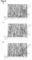
- Fig. 2 is a set of enlarged views illustrating root parts of scintillators.
- Fig. 2(a) is an enlarged view of the root part of the scintillator in the scintillator panel of this embodiment
- Fig. 2(b) is an enlarged view of the root part of a scintillator in a conventional scintillator panel.
- the conventional scintillator panel (also referred to as "conventional product” in the following) is one in which the scintillator 4 is formed by vapor deposition on the front face 2a of the FOP 2 without forming the heat-resistant resin layer 3 therebetween (the same hereinafter).
- the crystallinity deteriorates in particular in the end part 4x on the FOP 2 side (i.e., the root part 4x on the vapor deposition start side), so that, for example, the crystal shape (pillar form) breaks into lumps while yielding large variations.
- the root part 4x is meant a crystal part from the front face 2a of the FOP 2 to about 30 ⁇ m thereabove (the same also applies to the following root part 4x).
- the crystallinity in the root part 4x of the scintillator 4 is improved and made favorable in this embodiment as illustrated in Fig. 2(a) .
- the columnar crystal in the root part 4x beautifully extends straight while keeping its pillar form with less variations.
- the columnar crystal in the root part 4x (on the FOP 2 side) has a pillar form substantially equal to that of the columnar crystal on the leading end side (on the side opposite from the FOP 2). This greatly ameliorates the passability of emission (output), so as to improve the optical output, while inhibiting the scintillation light from scattering, whereby the resolution becomes higher.
- the scintillator 4 is favorably vapor-deposited when formed by vapor deposition on the heat-resistant resin layer 3. This seems to be because of the fact that, in the heat-resistant resin layer 3, the surface energy of its front face 3a becomes so low that, when a vapor flow (gas) of CsI attaches thereto, fine particles of CsI are likely to shrink, thereby making it easier for columnar crystals to form from early stages of vapor deposition.
- the FOP 2 is heated when manufacturing the scintillator panel 1 in this embodiment.
- the columnar crystal is thicker in the root part 4x of the scintillator 4.
- Fig. 3 is a result of experiments illustrating the correlation between the surface energy of heat-resistant resin layers and the crystallinity of scintillators.
- “O" and "X” mean that the crystallinity in the root part 4x is favorable and poor, respectively.
- Each of samples A to C is a scintillator panel in which the heat-resistant resin layer 3 is formed by a silicone resin.
- the curing condition for the heat-resistant resin layer 3 is A-, B-, and C-stages for the samples A, B, and C, respectively.
- the heat-resistant resin layer 3 contains a white pigment.
- Sample D is a scintillator panel in which the heat-resistant resin layer 3 is formed by poly(p-xylylene).
- the crystallinity in the root part 4x is favorable in the samples A, B, and C in which the surface energy of the front face 3a is 32.7 [mN/m], 24.8 [mN/m], and 30.8 [mN/m], respectively.
- the crystallinity in the root part 4x is poor in the sample D in which the surface energy of the front face 3a is 41.8 [mN/m].
- the surface energy of the front face 3a of the heat-resistant resin layer 3 is at least 20 [mN/m] but less than 35 [mN/m], more preferably at least 24.8 [mN/m] but less than 32.7 [mN/m], in this embodiment. Therefore, this embodiment can make the crystallinity of the root part 4x favorable, so as to inhibit the root part 4x from becoming harder to transmit and easier to scatter the scintillation light, whereby the optical output and resolution of the scintillator panel can be improved.
- Fig. 4 is a set of enlarged views of a scintillator illustrating the correlation between the curing condition of a heat-resistant layer and the crystallinity of the scintillator.
- the heat-resistant resin layer 3 is formed by a silicone resin
- the curing condition for the heat-resistant resin layer 3 is the A-, B-, and C-stages in Figs. 4(a), 4(b), and 4(c) , respectively.
- the crystallinity has improved in the root part 4x in each of the curing conditions at the A-, B-, and C-stages.
- the columnar crystal in the root part 4x at the B- and C-stages ( Figs. 4(b) and 4(c) ) is more likely to keep its pillar form and remain in a long monolithic state than that at the A-stage ( Figs. 4(a) ).
- the crystallinity of the root part 4x is better in the B-stage than in the C-stage.
- the curing condition for the heat-resistant resin layer 3 is preferably any of the A- to C-stages, more preferably the B- or C-stage, further preferably the B-stage, in this embodiment. This can inhibit the root part 4x from becoming harder to transmit and easier to scatter the scintillation light, whereby the optical output and resolution of the scintillator panel 1 can be improved.
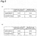
- Figs. 5 and 6 are a set of charts and graph illustrating tendencies of the optical output and resolution of scintillator panels.
- the abscissa indicates the relative value of resolution measured at 10 [Lp/mm] by using a CFT chart.
- the ordinate indicates the relative value of the optical output.
- the irradiation condition for the radiation R is a tube voltage of 30 kV with a tube current of 1.5 mA.
- the scintillator panel in accordance with the present invention is not limited to the above-mentioned scintillator panel in accordance with the embodiment, but may also be any of modifications within a scope not changing the gist set forth in each claim or one applied to others.
- a radiation-transmitting substrate metal substrate, carbon substrate, resin substrate, or the like
- the radiation image passes through the substrate 52, so as to be made incident on the scintillator 4 and thereby converted into a visible light image corresponding to the radiation image.
- the visible light image is emitted from the leading end side of the scintillator 4, so as to be detected by an image sensor optically coupled thereto.
- a light-reflecting film may be interposed between the substrate 52 and the heat-resistant resin layer 3, so that the heat-resistant resin layer 3 is disposed on the front face of the light reflecting film. This is also effective in preventing the light-reflecting film, when it is a metal film, from corroding under the influence of moisture and the like.
- the substrate may be an image sensor 76, on which the heat-resistant resin layer 3 is formed (the radiation image conversion panel being also referred to as radiation detector when the substrate is the image sensor 76).
- the image sensor 76 can be constructed as follows.
- an insulating substrate 62 which is made of glass, for example
- light-receiving devices 72 which perform photoelectric conversion are arranged two-dimensionally, so as to form a light-receiving section.
- Each light-receiving device 72 is constituted by a photodiode (PD) made of amorphous silicon or a thin-film transistor (TFT).
- PD photodiode
- TFT thin-film transistor
- a plurality of bonding pads 74 for taking out signals to external circuits are arranged so as to be exposed along the outer periphery of the substrate 62 and electrically connected to the light-receiving device 72 through the signal lines 73.
- An insulating passivation film 75 is formed on the light-receiving devices 72 and signal lines 73.
- the outer peripheral part of the protective film 5 is coated with a coating resin 82.
- the crystal form becomes favorable in the root part (on the vapor deposition start side) 4x of the scintillator 4 as mentioned above.
- the present invention exhibits remarkable effects when employed in one emitting the scintillation light from the root part 4x side of the scintillator 4 (the scintillator panel (radiation detector) equipped with the FOP 2 or image sensor 76 as the substrate).
- pillar form substantially equal is meant in a broad sense including pillar forms identical to each other, similar to (like) each other, approximating each other, and the like.
- the heat-resistant resin layer 3 in the above-mentioned embodiment is constructed such that the columnar crystal in the root part 4x of the scintillator 4 has a pillar form, for example, as illustrated in the following. This seems to be because the crystallinity of the columnar crystal in the root part 4x has a correlation with at least one of the elasticity, thermal expansion coefficient, contractility, surface state, and lattice constant of the heat-resistant resin layer 3.
- the elasticity of the heat-resistant resin layer 3 is in a predetermined elasticity region and/or its thermal expansion coefficient is in a predetermined thermal expansion coefficient region, so that the columnar crystal is constructed into a pillar form in the root part 4x.
- the heat-resistant resin layer 3 has a predetermined contractility, so that the columnar crystal is constructed into a pillar form in the root part 4x.
- the surface state of the heat-resistant resin layer 3 is set appropriately, so that the columnar crystal is constructed into a pillar form in the root part 4x.
- the lattice constant of the heat-resistant resin layer 3 is matched appropriately, so that the columnar crystal is constructed into a pillar form in the root part 4x.
- the surface energy may be adjusted not only by the kind of resin or the curing method, but also by irradiation with UV rays or electron beams.
- CsI(Na), NaI(Tl), LiI(Eu), KI(Tl), or the like may also be used as the scintillator 4 without being restricted to CsI(Tl) employed in the above-mentioned embodiment.
- the radiation image conversion panel is explained in terms of a scintillator panel using a scintillator for a phosphor in the above, the present invention is also applicable to radiation image conversion panels using photostimulable phosphors constituted by columnar crystals of CsBr(Eu) and the like.
- heat-resistant resin layer (resin layer) 3 it is sufficient for the heat-resistant resin layer (resin layer) 3 to exist in an effective region of the scintillator (phosphor) 4, while the heat-resistant resin layer 3 and scintillator 4 may have the same area or any of them may have an area larger than the other.
- the present invention can improve the optical output and resolution in radiation image conversion panels.
- 1...scintillator panel radiation image conversion panel
- 2...fiber optic plate substrate
- 2a...front face main face of the fiber optic plate
- 3...heat-resistant resin layer refsin layer
- 3a...front face (main face) of the heat-resistant resin layer 4...scintillator (phosphor); 52...substrate; 76...image sensor (substrate)
Abstract
Description
- The present invention relates to a radiation image conversion panel.
- As a scintillator panel, which is a kind of conventional radiation image conversion panels, one comprising a substrate, a resin layer formed on the substrate, and a scintillator (phosphor) formed by vapor deposition on the resin layer and made of a columnar crystal has been known (see, for example, Patent Literatures 1 and 2).
- Also known as a scintillator panel, which is a kind of conventional radiation image conversion panels, is one comprising a fiber optic plate (hereinafter also referred to as "FOP") and a scintillator (phosphor) formed by vapor deposition on the resin layer and made of a columnar crystal as disclosed in
Patent Literature 3, for example. This scintillator panel is covered with a film, so as to be secured and supported. -
- Patent Literature 1: Japanese Patent Application Laid-Open No.
2004-61115 - Patent Literature 2: Japanese Patent Application Laid-Open No.
2008-209124 - Patent Literature 3: Japanese Patent Publication No.
5-39558 - In the above-mentioned scintillator panel, crystallinity may deteriorate in a substrate-side end part (FOP-side end part, i.e., root part) of the vapor-deposited scintillator, thereby making the root part harder to transmit and easier to scatter scintillation light. As a result, there is a case where the above-mentioned scintillator panel lowers its optical output and resolution.
- It is therefore an object of the present invention to provide a radiation image conversion panel which can improve the optical output and resolution.
- For achieving the above-mentioned object, the inventors conducted diligent studies and, as a result, have found out that there is a correlation between the surface energy (surface tension) of a main face of a resin layer on which a phosphor is formed by vapor deposition and the crystallinity of the root part of the phosphor. Then, the inventors have thought up that the crystallinity of the root part of the phosphor can be made favorable if the surface energy is appropriate and thus completed the present invention.
- That is, in one aspect, the radiation image conversion panel in accordance with the present invention comprises a substrate, a resin layer formed on a main face of the substrate, and a phosphor formed by vapor deposition on a main face of the resin layer on a side opposite from the substrate and made of a columnar crystal, wherein at least the main face of the resin layer has a surface energy of at least 20 [mN/m] but less than 35 [mN/m].
- This radiation image conversion panel can inhibit the root part of the phosphor from becoming harder to transmit and easier to scatter output light (e.g., photostimulated luminescence or scintillation light), whereby the optical output and resolution of the radiation image conversion panel can be improved. This is because of the fact that the crystallinity of the root part of the phosphor becomes favorable when the main face of the resin layer where the phosphor is formed by vapor deposition has a surface energy of at least 20 [mN/m] but less than 35 [mN/m].
- Here is a case where the resin layer is formed by a silicone resin. There is also a case where the resin layer is formed by a step-cured resin subjected to a step-by-step curing process.
- Preferably, the surface energy of at least the main face of the resin layer is set according to the crystallinity of the phosphor. In this case, appropriately setting the surface energy of the main face of the resin layer, for example, can make the crystallinity of the phosphor favorable, thereby improving the optical output and resolution of the radiation image conversion panel.
- In another aspect, the radiation image conversion panel in accordance with the present invention comprises a substrate, a resin layer formed on a main face of the substrate, and a phosphor formed by vapor deposition on a main face of the resin layer on a side opposite from the substrate and made of a columnar crystal, wherein the phosphor is constructed such that the columnar crystal has a pillar form on the substrate side.
- In still another aspect, the radiation image conversion panel in accordance with the present invention comprises a substrate, a resin layer formed on a main face of the substrate, and a phosphor formed by vapor deposition on a main face of the resin layer on a side opposite from the substrate and made of a columnar crystal, wherein the columnar crystal on the substrate side of the phosphor has a pillar form substantially equal to that of the columnar crystal on the opposite side.
- Any of these aspects of the present invention can make the crystallinity of the root part of the phosphor favorable, so as to inhibit the root part of the phosphor from becoming harder to transmit and easier to scatter the output light, whereby the optical output and resolution of the radiation image conversion panel can be improved.
- There are cases where the substrate is a radiation-transmitting substrate, a fiber optic plate, and an image sensor, respectively.
- Also, for achieving the above-mentioned object, the inventors conducted diligent studies and, as a result, have found that forming a phosphor by vapor deposition on a heat-resistant resin layer can favorably vapor-deposit the phosphor, whereby the crystallinity of the root part of the phosphor can be made favorable. Then, the inventors have thought up that the optical output and resolution of the radiation image conversion panel can be improved according to the finding and thus completed the present invention.
- That is, in yet another aspect, the radiation image conversion panel in accordance with the present invention is a radiation image conversion panel comprising a fiber optic plate constituted by a bundle of a plurality of optical fibers and a phosphor made of a columnar crystal, the radiation image conversion panel further comprising a heat-resistant resin layer formed on a main face of the fiber optic plate and transparent to output light emitted from the phosphor, wherein the phosphor is formed by vapor deposition on a main face of the heat-resistant resin layer on a side opposite from the fiber optic plate.
- In this radiation image conversion panel, a heat-resistant resin layer transparent to output light (e.g., photostimulated luminescence or scintillation light) is formed on a FOP, while a phosphor is formed by vapor deposition on a main face of the heat-resistant resin layer. Therefore, because of the reason mentioned above, the crystallinity of the root part of the phosphor made of the columnar crystal can be favorable, so as to inhibit the root part from becoming harder to transmit and easier to scatter the output light. Hence, the optical output and resolution of the radiation image conversion panel can be improved.
- Here is a case where the resin layer is formed by a silicone resin. There is also a case where the resin layer is formed by a step-cured resin subjected to a step-by-step curing process.
- Preferably, a curing condition of the heat-resistant resin layer is set according to the crystallinity of the phosphor. In this case, appropriately setting the curing condition of the resin layer, for example, can make the crystallinity of the phosphor favorable, thereby improving the optical output and resolution of the radiation image conversion panel.
- In a further aspect, the radiation image conversion panel in accordance with the present invention is a radiation image conversion panel comprising a fiber optic plate constituted by a bundle of a plurality of optical fibers, a heat-resistant resin layer formed on a main face of the fiber optic plate, and a phosphor formed by vapor deposition on a main face of the heat-resistant layer on a side opposite from the fiber optic plate and made of a columnar crystal, wherein the phosphor is constructed such that the columnar crystal has a pillar form on the fiber optic plate side.
- In a still further aspect, the radiation image conversion panel in accordance with the present invention is a radiation image conversion panel comprising a fiber optic plate constituted by a bundle of a plurality of optical fibers, a heat-resistant resin layer formed on a main face of the fiber optic plate, and a phosphor formed by vapor deposition on a main face of the heat-resistant layer on a side opposite from the fiber optic plate and made of a columnar crystal, wherein the columnar crystal on the fiber optic plate side of the phosphor has a pillar form substantially equal to that of the columnar crystal on the opposite side.
- Any of these aspects of the present invention can make the crystallinity of the root part of the phosphor favorable, so as to inhibit the root part of the phosphor from becoming harder to transmit and easier to scatter the output light emitted from the phosphor, whereby the optical output and resolution of the radiation image conversion panel can be improved.
- The present invention can improve the optical output and resolution in radiation image conversion panels.
-
- [
Fig. 1 ] is a schematic side sectional view illustrating the scintillator panel in accordance with an embodiment of the present invention; - [
Fig. 2 ] is a set of enlarged views illustrating root parts of columnar crystalline scintillators; - [
Fig. 3 ] is a result of experiments illustrating the correlation between the surface energy of heat-resistant resin layers and the crystallinity of scintillators; - [
Fig. 4 ] is a set of enlarged views of a scintillator illustrating the correlation between the curing condition of a heat-resistant layer and the crystallinity of the scintillator; - [
Fig. 5 ] is a set of charts illustrating tendencies of the optical output and resolution of scintillator panels; - [
Fig. 6 ] is a graph illustrating tendencies of the optical output and resolution of scintillator panels; - [
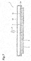
Fig. 7 ] is a schematic side sectional view illustrating a modified example of the present invention; and - [
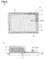
Fig. 8 ] (a) is a schematic plan view illustrating another modified example of the present invention, while (b) is a sectional view taken along the line VIII(b)-VIII(b) ofFig. 8(a) . - In the following, preferred embodiments of the present invention will be explained in detail with reference to the drawings. In the following explanations, the same or equivalent constituents will be referred to with the same signs, while omitting their overlapping descriptions.
- A scintillator panel, which is a radiation image conversion panel, will now be explained.
Fig. 1 is a schematic side sectional view illustrating the scintillator panel in accordance with an embodiment of the present invention. As illustrated inFig. 1 , the scintillator panel (radiation image conversion panel) 1 in accordance with this embodiment is used for converting a radiation R such as an x-ray incident thereon into scintillation light and detecting it. Here, the scintillator panel 1 is of a FOS (Fiber Optic plate with x-ray Scintillation) type using a FOP as a substrate. The scintillator panel 1 is used in mammography systems, breast screening systems, CT systems, and dental intraoral photography systems, for example. - The scintillator panel 1 comprises an FOP (substrate) 2, a heat-resistant resin layer (resin layer) 3 disposed on a front face (main face) 2a of the
FOP 2, a scintillator (phosphor) 4 formed by vapor deposition on a front face (main face) 3a of the heat-resistant resin layer 3 on the side opposite from theFOP 2, and aprotective layer 5 provided so as to cover theFOP 2, heat-resistant resin layer 3, andscintillator 4. - The
FOP 2 is an optical device constructed by a bundle of optical fibers each having a size of several microns, for example. The FOP 2 has a rectangular plate form. A photoelectric conversion element (not depicted) such as an image pickup device is optically coupled to theFOP 2. As a consequence, the scintillation light is transmitted to the photoelectric conversion element with high efficiency and low distortion. - The heat-
resistant layer 3 is a resin layer (so-called clear resin layer) transparent to the scintillation light. The heat-resistant layer 3 is formed by being applied to thefront face 2a of theFOP 2. The heat-resistant layer 3 has such a predetermined heat resistance as to be able to endure at least the heating at the time of vapor-depositing thescintillator 4. - By "transparent" is meant herein having such a property as to transmit therethrough "light to which the photoelectric conversion element optically coupled to the
FOP 2 is sensitive." Therefore, when utilizing a photoelectric conversion element having a sensitivity in a specific wavelength band in visible light, for example, the heat-resistant resin layer 3 may be nontransparent to the visible light on the outside of the sensitive region. When employing a photoelectric conversion element which is sensitive to infrared or ultraviolet rays instead of the visible light, the heat-resistant resin layer 3 may be nontransparent to the visible light as long as it can transmit therethrough light to which the photoelectric conversion element is sensitive. Hence, the heat-resistant resin layer 3 may be colored not only transparent, but also semitransparent gray or the like in order to adjust the optical output. - The
scintillator 4 is a phosphor layer which converts the incident radiation R into the scintillation light. Thescintillator 4 emits light according to the dose of the incident radiation R. Thescintillator 4 is formed by vacuum vapor deposition of T1 (thallium)-doped CsI (cesium iodide), which is constituted by a forest of a plurality of columnar crystals (acicular crystals each having a column diameter of several µm), on thefront face 3a of the heat-resistant resin layer 3. - The
protective layer 5 is used for protecting theFOP 2, heat-resistant resin layer 3, andscintillator 4 against moisture and the like. Theprotective layer 5 is formed by CVD (chemical vapor deposition) so as to cover theFOP 2, heat-resistant resin layer 3, andscintillator 4. An organic film such as one made of poly(p-xylylene) or an inorganic film is used as theprotective layer 5. - Here, the heat-
resistant resin layer 3 of this embodiment is formed by a silicone resin. In other words, the heat-resistant resin layer 3 is a silicone-based resin layer mainly composed of a silicone resin. The heat-resistant resin layer 3 is formed by applying a resin and then curing it by heat, which includes that of normal temperature, or by irradiation with light. The resin may also be a step-cured resin which completely cures through a step-by-step curing process. - At least the
front face 3a of the heat-resistant resin layer 3 has a surface energy which is preferably at least 20 [mN/m] but less than 35 [mN/m], more preferably at least 24.8 [mN/m] but less than 32.7 [mN/m]. A typical silicone resin has a surface energy of about 20 [mN/m]. - The surface energy in this embodiment is determined by measuring contact angles of test liquids at room temperature and decomposing the solid surface tension into components (three components) by using the extended Fowkes' equation. Specifically, contact angles are measured five times at respective positions where each test liquid is dropped and then are averaged. From thus obtained average value, dispersion, polar, and hydrogen-bonding components are calculated by using the extended Fowkes' equation. The sum of these components is determined as the surface energy. For measuring the contact angles, the static drop method is used, for example. Specifically, a droplet dropped on a surface to be measured is captured in a horizontal direction by a CCD camera, and then thus obtained droplet image is subjected to image processing, so as to measure the contact angle. A plurality of kinds of liquids (four kinds, i.e., water, formamide, diiodomethane, and ethylene glycol, here) are used as the test liquids.
- In a scintillator panel of a type using a radiation-transmitting substrate in place of the
FOP 2 so as to input a radiation image from the substrate side and emit a visible light image corresponding to the radiation image from the leading end side of thescintillator 4, the heat-resistant resin layer 3 may be formed by a silicone resin containing a pigment so as to function as a reflecting film for increasing the optical output of the scintillator panel 1, for example. A white pigment, a metal, or the like can be used as the pigment. Using the white pigment can enhance the diffuse reflection ratio, thereby further raising the optical output. The heat-resistant resin layer 3 is not limited to those formed by silicone resins as in this embodiment, but may be formed by any of other resins. - The radiation R (radiation image) is incident on thus constructed scintillator panel 1 from the
front face 2a side (the upper side in the drawing, i.e., on the light entrance surface side) of theFOP 2 in the scintillator 4 (i.e., the radiation R enters from the leading end side of the scintillator 4). The radiation R passes through theprotective layer 5, so as to be made incident on and absorbed by thescintillator 4, thereby being converted into scintillation light (visible light image) having a predetermined wavelength in proportion to the quantity of the radiation R. Thus converted scintillation light passes through the heat-resistant resin layer 3, so as to reach theFOP 2. TheFOP 2 transmits the visible light image to the optical output surface of theFOP 2. - Thus constructed scintillator panel 1 can be manufactured by a method illustrated in the following, for example. The
FOP 2 is initially washed with wash water, and then thefront face 2a of theFOP 2 is coated with the heat-resistant resin layer 3, which is thermally cured thereafter. - Here, the heat-
resistant resin layer 3 is a step-cured resin as mentioned above, which is preferably in the B-stage. - A-stage: Immediately after coating with the heat-resistant resin layer 3 (without firing).
- B-stage: Stage in the process of the curing reaction of the heat-
resistant resin layer 3 fired after coating. - C-stage: Stage where the heat-
resistant resin layer 3 is completely cured after coating. - Subsequently, the
FOP 2 is heated at 100°C, for example, and then CsI is formed into a film by oblique vapor deposition on thefront face 3a of the heat-resistant resin layer 3, so as to form thescintillator 4. Thereafter, theprotective layer 5 is formed so as to cover theFOP 2, heat-resistant resin layer 3, andscintillator 4. This can yield the scintillator panel 1. -
Fig. 2 is a set of enlarged views illustrating root parts of scintillators.Fig. 2(a) is an enlarged view of the root part of the scintillator in the scintillator panel of this embodiment, whereasFig. 2(b) is an enlarged view of the root part of a scintillator in a conventional scintillator panel. The conventional scintillator panel (also referred to as "conventional product" in the following) is one in which thescintillator 4 is formed by vapor deposition on thefront face 2a of theFOP 2 without forming the heat-resistant resin layer 3 therebetween (the same hereinafter). - In the vapor-deposited
scintillator 4 in the conventional product, as illustrated inFig. 2(b) , the crystallinity deteriorates in particular in theend part 4x on theFOP 2 side (i.e., theroot part 4x on the vapor deposition start side), so that, for example, the crystal shape (pillar form) breaks into lumps while yielding large variations. Hence, there is a fear of theroot part 4x becoming harder to transmit and easier to scatter the scintillation light in the conventional product. By theroot part 4x is meant a crystal part from thefront face 2a of theFOP 2 to about 30 µm thereabove (the same also applies to the followingroot part 4x). - In this regard, the crystallinity in the
root part 4x of thescintillator 4 is improved and made favorable in this embodiment as illustrated inFig. 2(a) . Specifically, the columnar crystal in theroot part 4x beautifully extends straight while keeping its pillar form with less variations. In other words, in thescintillator 4, the columnar crystal in theroot part 4x (on theFOP 2 side) has a pillar form substantially equal to that of the columnar crystal on the leading end side (on the side opposite from the FOP 2). This greatly ameliorates the passability of emission (output), so as to improve the optical output, while inhibiting the scintillation light from scattering, whereby the resolution becomes higher. - This is because the
scintillator 4 is favorably vapor-deposited when formed by vapor deposition on the heat-resistant resin layer 3. This seems to be because of the fact that, in the heat-resistant resin layer 3, the surface energy of itsfront face 3a becomes so low that, when a vapor flow (gas) of CsI attaches thereto, fine particles of CsI are likely to shrink, thereby making it easier for columnar crystals to form from early stages of vapor deposition. - Meanwhile, as mentioned above, the
FOP 2 is heated when manufacturing the scintillator panel 1 in this embodiment. Hence, the columnar crystal is thicker in theroot part 4x of thescintillator 4. -
Fig. 3 is a result of experiments illustrating the correlation between the surface energy of heat-resistant resin layers and the crystallinity of scintillators. In the chart, "O" and "X" mean that the crystallinity in theroot part 4x is favorable and poor, respectively. Each of samples A to C is a scintillator panel in which the heat-resistant resin layer 3 is formed by a silicone resin. The curing condition for the heat-resistant resin layer 3 is A-, B-, and C-stages for the samples A, B, and C, respectively. In the sample C, the heat-resistant resin layer 3 contains a white pigment. Sample D is a scintillator panel in which the heat-resistant resin layer 3 is formed by poly(p-xylylene). - As illustrated in
Fig. 3 , the crystallinity in theroot part 4x is favorable in the samples A, B, and C in which the surface energy of thefront face 3a is 32.7 [mN/m], 24.8 [mN/m], and 30.8 [mN/m], respectively. By contrast, it is seen that the crystallinity in theroot part 4x is poor in the sample D in which the surface energy of thefront face 3a is 41.8 [mN/m]. - Hence, as mentioned above, the surface energy of the
front face 3a of the heat-resistant resin layer 3 is at least 20 [mN/m] but less than 35 [mN/m], more preferably at least 24.8 [mN/m] but less than 32.7 [mN/m], in this embodiment. Therefore, this embodiment can make the crystallinity of theroot part 4x favorable, so as to inhibit theroot part 4x from becoming harder to transmit and easier to scatter the scintillation light, whereby the optical output and resolution of the scintillator panel can be improved. -
Fig. 4 is a set of enlarged views of a scintillator illustrating the correlation between the curing condition of a heat-resistant layer and the crystallinity of the scintillator. In the drawings, the heat-resistant resin layer 3 is formed by a silicone resin, while the curing condition for the heat-resistant resin layer 3 is the A-, B-, and C-stages inFigs. 4(a), 4(b), and 4(c) , respectively. - It is seen from
Fig. 4 that the crystallinity has improved in theroot part 4x in each of the curing conditions at the A-, B-, and C-stages. In particular, the columnar crystal in theroot part 4x at the B- and C-stages (Figs. 4(b) and 4(c) ) is more likely to keep its pillar form and remain in a long monolithic state than that at the A-stage (Figs. 4(a) ). The crystallinity of theroot part 4x is better in the B-stage than in the C-stage. - Hence, as mentioned above, the curing condition for the heat-
resistant resin layer 3 is preferably any of the A- to C-stages, more preferably the B- or C-stage, further preferably the B-stage, in this embodiment. This can inhibit theroot part 4x from becoming harder to transmit and easier to scatter the scintillation light, whereby the optical output and resolution of the scintillator panel 1 can be improved. -
Figs. 5 and6 are a set of charts and graph illustrating tendencies of the optical output and resolution of scintillator panels. In the graph, the abscissa indicates the relative value of resolution measured at 10 [Lp/mm] by using a CFT chart. The ordinate indicates the relative value of the optical output. The irradiation condition for the radiation R is a tube voltage of 30 kV with a tube current of 1.5 mA. - The above-mentioned advantageous effect of improving the optical output and resolution can be seen from the results illustrated in
Figs. 5 and6 . As illustrated inFig. 5 , an improvement of 10% or more over the conventional product is seen in each of the optical output and resolution in this embodiment. As illustrated inFig. 6 , the results show that the data of this embodiment is located on the upper right side of that of the conventional product. From this, it is seen that both of the optical output and resolution improve. - Though a preferred embodiment of the present invention is explained in the foregoing, the scintillator panel in accordance with the present invention is not limited to the above-mentioned scintillator panel in accordance with the embodiment, but may also be any of modifications within a scope not changing the gist set forth in each claim or one applied to others.
- For example, while the above-mentioned embodiment is equipped with the
FOP 2 as a substrate, a radiation-transmitting substrate (metal substrate, carbon substrate, resin substrate, or the like) 52 may be provided instead as illustrated inFig. 7 . When the substrate is the radiation-transmittingsubstrate 52, the radiation image passes through thesubstrate 52, so as to be made incident on thescintillator 4 and thereby converted into a visible light image corresponding to the radiation image. The visible light image is emitted from the leading end side of thescintillator 4, so as to be detected by an image sensor optically coupled thereto. - In this case, for increasing the optical output of the scintillator panel 1, a light-reflecting film may be interposed between the
substrate 52 and the heat-resistant resin layer 3, so that the heat-resistant resin layer 3 is disposed on the front face of the light reflecting film. This is also effective in preventing the light-reflecting film, when it is a metal film, from corroding under the influence of moisture and the like. - As illustrated in
Fig. 8 , the substrate may be animage sensor 76, on which the heat-resistant resin layer 3 is formed (the radiation image conversion panel being also referred to as radiation detector when the substrate is the image sensor 76). In this case, theimage sensor 76 can be constructed as follows. On an insulating substrate 62 (which is made of glass, for example), light-receivingdevices 72 which perform photoelectric conversion are arranged two-dimensionally, so as to form a light-receiving section. Each light-receivingdevice 72 is constituted by a photodiode (PD) made of amorphous silicon or a thin-film transistor (TFT). The light-receivingdevices 72 are electrically connected to each other throughsignal lines 73 for reading signals. A plurality ofbonding pads 74 for taking out signals to external circuits (not depicted) are arranged so as to be exposed along the outer periphery of thesubstrate 62 and electrically connected to the light-receivingdevice 72 through the signal lines 73. An insulatingpassivation film 75 is formed on the light-receivingdevices 72 and signal lines 73. The outer peripheral part of theprotective film 5 is coated with acoating resin 82. - In the present invention, the crystal form becomes favorable in the root part (on the vapor deposition start side) 4x of the
scintillator 4 as mentioned above. Hence, the present invention exhibits remarkable effects when employed in one emitting the scintillation light from theroot part 4x side of the scintillator 4 (the scintillator panel (radiation detector) equipped with theFOP 2 orimage sensor 76 as the substrate). - Various curing conditions can be employed without being restricted to the above-mentioned A- to C-stages as long as the crystallinity can be made favorable in the
root part 4x of thescintillator 4. In the above, "pillar form substantially equal" is meant in a broad sense including pillar forms identical to each other, similar to (like) each other, approximating each other, and the like. - There is a case where the heat-
resistant resin layer 3 in the above-mentioned embodiment is constructed such that the columnar crystal in theroot part 4x of thescintillator 4 has a pillar form, for example, as illustrated in the following. This seems to be because the crystallinity of the columnar crystal in theroot part 4x has a correlation with at least one of the elasticity, thermal expansion coefficient, contractility, surface state, and lattice constant of the heat-resistant resin layer 3. - That is, there is a case where the elasticity of the heat-
resistant resin layer 3 is in a predetermined elasticity region and/or its thermal expansion coefficient is in a predetermined thermal expansion coefficient region, so that the columnar crystal is constructed into a pillar form in theroot part 4x. There is also a case where the heat-resistant resin layer 3 has a predetermined contractility, so that the columnar crystal is constructed into a pillar form in theroot part 4x. Further, there is a case where the surface state of the heat-resistant resin layer 3 is set appropriately, so that the columnar crystal is constructed into a pillar form in theroot part 4x. Furthermore, there is a case where the lattice constant of the heat-resistant resin layer 3 is matched appropriately, so that the columnar crystal is constructed into a pillar form in theroot part 4x. - The surface energy may be adjusted not only by the kind of resin or the curing method, but also by irradiation with UV rays or electron beams. CsI(Na), NaI(Tl), LiI(Eu), KI(Tl), or the like may also be used as the
scintillator 4 without being restricted to CsI(Tl) employed in the above-mentioned embodiment. Though the radiation image conversion panel is explained in terms of a scintillator panel using a scintillator for a phosphor in the above, the present invention is also applicable to radiation image conversion panels using photostimulable phosphors constituted by columnar crystals of CsBr(Eu) and the like. - It is sufficient for the heat-resistant resin layer (resin layer) 3 to exist in an effective region of the scintillator (phosphor) 4, while the heat-
resistant resin layer 3 andscintillator 4 may have the same area or any of them may have an area larger than the other. - The present invention can improve the optical output and resolution in radiation image conversion panels.
- 1...scintillator panel (radiation image conversion panel); 2...fiber optic plate (substrate); 2a...front face (main face) of the fiber optic plate; 3...heat-resistant resin layer (resin layer); 3a...front face (main face) of the heat-resistant resin layer; 4...scintillator (phosphor); 52...substrate; 76...image sensor (substrate)
Claims (6)
- A radiation image conversion panel comprising a substrate, a resin layer formed on a main face of the substrate, and a phosphor formed by vapor deposition on a main face of the resin layer on a side opposite from the substrate and made of a columnar crystal;
wherein the phosphor is constructed such that the columnar crystal has a pillar form on the substrate side. - A radiation image conversion panel according to claim 1, wherein the substrate is a radiation-transmitting substrate.
- A radiation image conversion panel according to claim 1, wherein the substrate is a fiber optic plate.
- A radiation image conversion panel according to claim 1, wherein the substrate is an image sensor.
- A radiation image conversion panel according to one of claims 1 to 4, wherein the resin layer is formed by a silicone resin.
- A radiation image conversion panel according to one of claims 1 to 5, wherein the resin layer is formed by a step-cured resin subjected to a step-by-step curing process.
Applications Claiming Priority (4)
| Application Number | Priority Date | Filing Date | Title |
|---|---|---|---|
| JP2010018548A JP2011158291A (en) | 2010-01-29 | 2010-01-29 | Radiation image conversion panel |
| JP2010018563A JP5749439B2 (en) | 2010-01-29 | 2010-01-29 | Radiation image conversion panel |
| PCT/JP2011/050460 WO2011093140A1 (en) | 2010-01-29 | 2011-01-13 | Radiation image conversion panel |
| EP11736855.5A EP2530682B1 (en) | 2010-01-29 | 2011-01-13 | Radiation image conversion panel |
Related Parent Applications (2)
| Application Number | Title | Priority Date | Filing Date |
|---|---|---|---|
| EP11736855.5A Division EP2530682B1 (en) | 2010-01-29 | 2011-01-13 | Radiation image conversion panel |
| EP11736855.5A Division-Into EP2530682B1 (en) | 2010-01-29 | 2011-01-13 | Radiation image conversion panel |
Publications (2)
| Publication Number | Publication Date |
|---|---|
| EP3220392A1 true EP3220392A1 (en) | 2017-09-20 |
| EP3220392B1 EP3220392B1 (en) | 2021-09-15 |
Family
ID=44319131
Family Applications (2)
| Application Number | Title | Priority Date | Filing Date |
|---|---|---|---|
| EP11736855.5A Active EP2530682B1 (en) | 2010-01-29 | 2011-01-13 | Radiation image conversion panel |
| EP17169731.1A Active EP3220392B1 (en) | 2010-01-29 | 2011-01-13 | Radiation image conversion panel |
Family Applications Before (1)
| Application Number | Title | Priority Date | Filing Date |
|---|---|---|---|
| EP11736855.5A Active EP2530682B1 (en) | 2010-01-29 | 2011-01-13 | Radiation image conversion panel |
Country Status (6)
| Country | Link |
|---|---|
| US (1) | US8866088B2 (en) |
| EP (2) | EP2530682B1 (en) |
| KR (1) | KR101726464B1 (en) |
| CN (1) | CN102741941B (en) |
| TW (1) | TWI496165B (en) |
| WO (1) | WO2011093140A1 (en) |
Families Citing this family (10)
| Publication number | Priority date | Publication date | Assignee | Title |
|---|---|---|---|---|
| GB2477346B (en) * | 2010-02-01 | 2016-03-23 | Scintacor Ltd | Scintillator assembly for use in digital x-ray imaging |
| JP5844545B2 (en) * | 2010-05-31 | 2016-01-20 | 富士フイルム株式会社 | Radiography equipment |
| US20130015371A1 (en) * | 2011-07-11 | 2013-01-17 | General Electric Company | Thermoluminescent computed radiography reader and method for using same |
| TWI651539B (en) * | 2014-03-10 | 2019-02-21 | 美商瓊斯科技國際公司 | Wafer-level integrated circuit probe array and construction method |
| USD806249S1 (en) | 2014-12-16 | 2017-12-26 | Hamamatsu Photonics K.K. | Radiation image conversion plate |
| WO2016172291A1 (en) * | 2015-04-23 | 2016-10-27 | Fermi Research Alliance, Llc | Monocrystal-based microchannel plate image intensifier |
| JP6549950B2 (en) * | 2015-09-15 | 2019-07-24 | 浜松ホトニクス株式会社 | Scintillator panel and radiation detector |
| CN106443754B (en) * | 2016-11-16 | 2019-02-01 | 奕瑞影像科技(太仓)有限公司 | Radioscopic image capturing apparatus |
| CN106526653B (en) * | 2016-12-19 | 2023-02-28 | 桂林百锐光电技术有限公司 | Scintillation detector |
| JP7108364B2 (en) * | 2018-09-04 | 2022-07-28 | キヤノン電子管デバイス株式会社 | Radiation detector, radiation detector manufacturing method and apparatus, scintillator panel, scintillator panel manufacturing method and apparatus |
Citations (4)
| Publication number | Priority date | Publication date | Assignee | Title |
|---|---|---|---|---|
| JPH0539558A (en) | 1991-08-06 | 1993-02-19 | Nippon Steel Corp | Back-up roll of rotary brush |
| JP2004061115A (en) | 2002-07-24 | 2004-02-26 | Canon Inc | Scintillator panel, radiation detection device, and radiation imaging system |
| JP2008209124A (en) | 2007-02-23 | 2008-09-11 | Konica Minolta Medical & Graphic Inc | Scintillator panel |
| US7548608B2 (en) * | 2006-04-26 | 2009-06-16 | Siemens Aktiengesellschaft | Flat X-ray detector and method for controlling the image dose emitted by an X-ray tube to a flat X-ray detector when recording an X-ray image |
Family Cites Families (12)
| Publication number | Priority date | Publication date | Assignee | Title |
|---|---|---|---|---|
| JPS63215987A (en) * | 1987-03-04 | 1988-09-08 | Hamamatsu Photonics Kk | Highly resolvable scintillation fiber plate |
| JPH0539558Y2 (en) | 1987-09-02 | 1993-10-07 | ||
| JP3819347B2 (en) * | 2002-09-05 | 2006-09-06 | 富士写真フイルム株式会社 | Radiation image conversion panel |
| WO2004079396A1 (en) * | 2003-03-07 | 2004-09-16 | Hamamatsu Photonics K.K. | Scintillator panel and method of manufacturing radiation image sensor |
| US7355184B2 (en) * | 2003-04-07 | 2008-04-08 | Canon Kabushiki Kaisha | Radiation detecting apparatus and method for manufacturing the same |
| JP4208687B2 (en) | 2003-09-29 | 2009-01-14 | 株式会社東芝 | Image sensor |
| CN101002110B (en) * | 2004-08-10 | 2010-12-08 | 佳能株式会社 | Radiation detecting apparatus, scintillator panel, their manufacturing method and radiation detecting system |
| JP2006250909A (en) * | 2005-03-14 | 2006-09-21 | Fuji Photo Film Co Ltd | Radiation image conversion panel |
| US20080095997A1 (en) * | 2006-10-19 | 2008-04-24 | Tien-Hon Chiang | Function-Enhancing Optical Film |
| KR101393776B1 (en) | 2007-03-27 | 2014-05-12 | 도시바 덴시칸 디바이스 가부시키가이샤 | Scintillator panel and manufacturing method thereof, amd radiation detector |
| JP5004848B2 (en) | 2007-04-18 | 2012-08-22 | キヤノン株式会社 | Radiation detection apparatus and radiation detection system |
| CN101886675B (en) * | 2010-06-30 | 2012-10-03 | 浙江大学 | Semi-automatic electrically controlled clutch system |
-
2011
- 2011-01-13 KR KR1020127006503A patent/KR101726464B1/en active IP Right Grant
- 2011-01-13 US US13/522,568 patent/US8866088B2/en active Active
- 2011-01-13 WO PCT/JP2011/050460 patent/WO2011093140A1/en active Application Filing
- 2011-01-13 EP EP11736855.5A patent/EP2530682B1/en active Active
- 2011-01-13 EP EP17169731.1A patent/EP3220392B1/en active Active
- 2011-01-13 CN CN201180007472.4A patent/CN102741941B/en active Active
- 2011-01-24 TW TW100102483A patent/TWI496165B/en active
Patent Citations (4)
| Publication number | Priority date | Publication date | Assignee | Title |
|---|---|---|---|---|
| JPH0539558A (en) | 1991-08-06 | 1993-02-19 | Nippon Steel Corp | Back-up roll of rotary brush |
| JP2004061115A (en) | 2002-07-24 | 2004-02-26 | Canon Inc | Scintillator panel, radiation detection device, and radiation imaging system |
| US7548608B2 (en) * | 2006-04-26 | 2009-06-16 | Siemens Aktiengesellschaft | Flat X-ray detector and method for controlling the image dose emitted by an X-ray tube to a flat X-ray detector when recording an X-ray image |
| JP2008209124A (en) | 2007-02-23 | 2008-09-11 | Konica Minolta Medical & Graphic Inc | Scintillator panel |
Also Published As
| Publication number | Publication date |
|---|---|
| US20120312998A1 (en) | 2012-12-13 |
| KR101726464B1 (en) | 2017-04-12 |
| CN102741941B (en) | 2015-04-08 |
| WO2011093140A1 (en) | 2011-08-04 |
| EP2530682B1 (en) | 2019-11-20 |
| EP2530682A4 (en) | 2017-07-26 |
| CN102741941A (en) | 2012-10-17 |
| EP3220392B1 (en) | 2021-09-15 |
| TW201214464A (en) | 2012-04-01 |
| TWI496165B (en) | 2015-08-11 |
| EP2530682A1 (en) | 2012-12-05 |
| KR20120125222A (en) | 2012-11-14 |
| US8866088B2 (en) | 2014-10-21 |
Similar Documents
| Publication | Publication Date | Title |
|---|---|---|
| EP3220392B1 (en) | Radiation image conversion panel | |
| US6867418B2 (en) | Radiation image sensor and scintillator panel | |
| US8049177B2 (en) | Radiation image detection apparatus and manufacturing method of the same | |
| US8841621B2 (en) | Radiographic imaging apparatus | |
| US7977646B2 (en) | Scintillation detector reflector | |
| US9136029B2 (en) | Scintillator panel, and radiographic image sensor | |
| US9304212B2 (en) | Scintillator panel and manufacturing method therefor and radiation detector and manufacturing method therefor | |
| US9418768B2 (en) | Radiographic image conversion panel and radiographic image detector | |
| JP5749439B2 (en) | Radiation image conversion panel | |
| US10156640B2 (en) | Radiation detection apparatus and radiation detection sheet | |
| US10386505B2 (en) | Scintillator, scintillator panel, radiation detector and method of manufacturing scintillator | |
| JP6756170B2 (en) | Radiation image conversion panel | |
| JP2011158291A (en) | Radiation image conversion panel | |
| US20160172400A1 (en) | Photo detector and method for fabricating the same | |
| JP5937185B2 (en) | Manufacturing method of radiation image conversion panel | |
| TW201830053A (en) | Radiography detector and radiography imaging device | |
| US20230184967A1 (en) | Scintillator panel and radiation detector | |
| JP2012220400A (en) | Scintillator panel, method for manufacturing scintillator panel, and radiation detector | |
| KR101903268B1 (en) | Radiation detector and scintillator panel |
Legal Events
| Date | Code | Title | Description |
|---|---|---|---|
| PUAI | Public reference made under article 153(3) epc to a published international application that has entered the european phase |
Free format text: ORIGINAL CODE: 0009012 |
|
| STAA | Information on the status of an ep patent application or granted ep patent |
Free format text: STATUS: REQUEST FOR EXAMINATION WAS MADE |
|
| 17P | Request for examination filed |
Effective date: 20170505 |
|
| AC | Divisional application: reference to earlier application |
Ref document number: 2530682 Country of ref document: EP Kind code of ref document: P |
|
| AK | Designated contracting states |
Kind code of ref document: A1 Designated state(s): AL AT BE BG CH CY CZ DE DK EE ES FI FR GB GR HR HU IE IS IT LI LT LU LV MC MK MT NL NO PL PT RO RS SE SI SK SM TR |
|
| RBV | Designated contracting states (corrected) |
Designated state(s): AL AT BE BG CH CY CZ DE DK EE ES FI FR GB GR HR HU IE IS IT LI LT LU LV MC MK MT NL NO PL PT RO RS SE SI SK SM TR |
|
| STAA | Information on the status of an ep patent application or granted ep patent |
Free format text: STATUS: EXAMINATION IS IN PROGRESS |
|
| 17Q | First examination report despatched |
Effective date: 20190924 |
|
| STAA | Information on the status of an ep patent application or granted ep patent |
Free format text: STATUS: EXAMINATION IS IN PROGRESS |
|
| GRAP | Despatch of communication of intention to grant a patent |
Free format text: ORIGINAL CODE: EPIDOSNIGR1 |
|
| STAA | Information on the status of an ep patent application or granted ep patent |
Free format text: STATUS: GRANT OF PATENT IS INTENDED |
|
| INTG | Intention to grant announced |
Effective date: 20210428 |
|
| GRAS | Grant fee paid |
Free format text: ORIGINAL CODE: EPIDOSNIGR3 |
|
| GRAA | (expected) grant |
Free format text: ORIGINAL CODE: 0009210 |
|
| STAA | Information on the status of an ep patent application or granted ep patent |
Free format text: STATUS: THE PATENT HAS BEEN GRANTED |
|
| AC | Divisional application: reference to earlier application |
Ref document number: 2530682 Country of ref document: EP Kind code of ref document: P |
|
| AK | Designated contracting states |
Kind code of ref document: B1 Designated state(s): AL AT BE BG CH CY CZ DE DK EE ES FI FR GB GR HR HU IE IS IT LI LT LU LV MC MK MT NL NO PL PT RO RS SE SI SK SM TR |
|
| REG | Reference to a national code |
Ref country code: CH Ref legal event code: EP |
|
| REG | Reference to a national code |
Ref country code: DE Ref legal event code: R096 Ref document number: 602011071806 Country of ref document: DE |
|
| REG | Reference to a national code |
Ref country code: IE Ref legal event code: FG4D |
|
| REG | Reference to a national code |
Ref country code: AT Ref legal event code: REF Ref document number: 1431151 Country of ref document: AT Kind code of ref document: T Effective date: 20211015 |
|
| REG | Reference to a national code |
Ref country code: NL Ref legal event code: FP |
|
| REG | Reference to a national code |
Ref country code: LT Ref legal event code: MG9D |
|
| PG25 | Lapsed in a contracting state [announced via postgrant information from national office to epo] |
Ref country code: LT Free format text: LAPSE BECAUSE OF FAILURE TO SUBMIT A TRANSLATION OF THE DESCRIPTION OR TO PAY THE FEE WITHIN THE PRESCRIBED TIME-LIMIT Effective date: 20210915 Ref country code: BG Free format text: LAPSE BECAUSE OF FAILURE TO SUBMIT A TRANSLATION OF THE DESCRIPTION OR TO PAY THE FEE WITHIN THE PRESCRIBED TIME-LIMIT Effective date: 20211215 Ref country code: FI Free format text: LAPSE BECAUSE OF FAILURE TO SUBMIT A TRANSLATION OF THE DESCRIPTION OR TO PAY THE FEE WITHIN THE PRESCRIBED TIME-LIMIT Effective date: 20210915 Ref country code: HR Free format text: LAPSE BECAUSE OF FAILURE TO SUBMIT A TRANSLATION OF THE DESCRIPTION OR TO PAY THE FEE WITHIN THE PRESCRIBED TIME-LIMIT Effective date: 20210915 Ref country code: NO Free format text: LAPSE BECAUSE OF FAILURE TO SUBMIT A TRANSLATION OF THE DESCRIPTION OR TO PAY THE FEE WITHIN THE PRESCRIBED TIME-LIMIT Effective date: 20211215 Ref country code: SE Free format text: LAPSE BECAUSE OF FAILURE TO SUBMIT A TRANSLATION OF THE DESCRIPTION OR TO PAY THE FEE WITHIN THE PRESCRIBED TIME-LIMIT Effective date: 20210915 Ref country code: RS Free format text: LAPSE BECAUSE OF FAILURE TO SUBMIT A TRANSLATION OF THE DESCRIPTION OR TO PAY THE FEE WITHIN THE PRESCRIBED TIME-LIMIT Effective date: 20210915 |
|
| REG | Reference to a national code |
Ref country code: AT Ref legal event code: MK05 Ref document number: 1431151 Country of ref document: AT Kind code of ref document: T Effective date: 20210915 |
|
| PG25 | Lapsed in a contracting state [announced via postgrant information from national office to epo] |
Ref country code: LV Free format text: LAPSE BECAUSE OF FAILURE TO SUBMIT A TRANSLATION OF THE DESCRIPTION OR TO PAY THE FEE WITHIN THE PRESCRIBED TIME-LIMIT Effective date: 20210915 Ref country code: GR Free format text: LAPSE BECAUSE OF FAILURE TO SUBMIT A TRANSLATION OF THE DESCRIPTION OR TO PAY THE FEE WITHIN THE PRESCRIBED TIME-LIMIT Effective date: 20211216 |
|
| PG25 | Lapsed in a contracting state [announced via postgrant information from national office to epo] |
Ref country code: AT Free format text: LAPSE BECAUSE OF FAILURE TO SUBMIT A TRANSLATION OF THE DESCRIPTION OR TO PAY THE FEE WITHIN THE PRESCRIBED TIME-LIMIT Effective date: 20210915 |
|
| PG25 | Lapsed in a contracting state [announced via postgrant information from national office to epo] |
Ref country code: IS Free format text: LAPSE BECAUSE OF FAILURE TO SUBMIT A TRANSLATION OF THE DESCRIPTION OR TO PAY THE FEE WITHIN THE PRESCRIBED TIME-LIMIT Effective date: 20220115 Ref country code: SM Free format text: LAPSE BECAUSE OF FAILURE TO SUBMIT A TRANSLATION OF THE DESCRIPTION OR TO PAY THE FEE WITHIN THE PRESCRIBED TIME-LIMIT Effective date: 20210915 Ref country code: SK Free format text: LAPSE BECAUSE OF FAILURE TO SUBMIT A TRANSLATION OF THE DESCRIPTION OR TO PAY THE FEE WITHIN THE PRESCRIBED TIME-LIMIT Effective date: 20210915 Ref country code: RO Free format text: LAPSE BECAUSE OF FAILURE TO SUBMIT A TRANSLATION OF THE DESCRIPTION OR TO PAY THE FEE WITHIN THE PRESCRIBED TIME-LIMIT Effective date: 20210915 Ref country code: PT Free format text: LAPSE BECAUSE OF FAILURE TO SUBMIT A TRANSLATION OF THE DESCRIPTION OR TO PAY THE FEE WITHIN THE PRESCRIBED TIME-LIMIT Effective date: 20220117 Ref country code: PL Free format text: LAPSE BECAUSE OF FAILURE TO SUBMIT A TRANSLATION OF THE DESCRIPTION OR TO PAY THE FEE WITHIN THE PRESCRIBED TIME-LIMIT Effective date: 20210915 Ref country code: ES Free format text: LAPSE BECAUSE OF FAILURE TO SUBMIT A TRANSLATION OF THE DESCRIPTION OR TO PAY THE FEE WITHIN THE PRESCRIBED TIME-LIMIT Effective date: 20210915 Ref country code: EE Free format text: LAPSE BECAUSE OF FAILURE TO SUBMIT A TRANSLATION OF THE DESCRIPTION OR TO PAY THE FEE WITHIN THE PRESCRIBED TIME-LIMIT Effective date: 20210915 Ref country code: CZ Free format text: LAPSE BECAUSE OF FAILURE TO SUBMIT A TRANSLATION OF THE DESCRIPTION OR TO PAY THE FEE WITHIN THE PRESCRIBED TIME-LIMIT Effective date: 20210915 Ref country code: AL Free format text: LAPSE BECAUSE OF FAILURE TO SUBMIT A TRANSLATION OF THE DESCRIPTION OR TO PAY THE FEE WITHIN THE PRESCRIBED TIME-LIMIT Effective date: 20210915 |
|
| REG | Reference to a national code |
Ref country code: DE Ref legal event code: R097 Ref document number: 602011071806 Country of ref document: DE |
|
| PLBE | No opposition filed within time limit |
Free format text: ORIGINAL CODE: 0009261 |
|
| STAA | Information on the status of an ep patent application or granted ep patent |
Free format text: STATUS: NO OPPOSITION FILED WITHIN TIME LIMIT |
|
| PG25 | Lapsed in a contracting state [announced via postgrant information from national office to epo] |
Ref country code: DK Free format text: LAPSE BECAUSE OF FAILURE TO SUBMIT A TRANSLATION OF THE DESCRIPTION OR TO PAY THE FEE WITHIN THE PRESCRIBED TIME-LIMIT Effective date: 20210915 |
|
| 26N | No opposition filed |
Effective date: 20220616 |
|
| PG25 | Lapsed in a contracting state [announced via postgrant information from national office to epo] |
Ref country code: SI Free format text: LAPSE BECAUSE OF FAILURE TO SUBMIT A TRANSLATION OF THE DESCRIPTION OR TO PAY THE FEE WITHIN THE PRESCRIBED TIME-LIMIT Effective date: 20210915 Ref country code: MC Free format text: LAPSE BECAUSE OF FAILURE TO SUBMIT A TRANSLATION OF THE DESCRIPTION OR TO PAY THE FEE WITHIN THE PRESCRIBED TIME-LIMIT Effective date: 20210915 |
|
| REG | Reference to a national code |
Ref country code: CH Ref legal event code: PL |
|
| REG | Reference to a national code |
Ref country code: BE Ref legal event code: MM Effective date: 20220131 |
|
| PG25 | Lapsed in a contracting state [announced via postgrant information from national office to epo] |
Ref country code: LU Free format text: LAPSE BECAUSE OF NON-PAYMENT OF DUE FEES Effective date: 20220113 |
|
| PG25 | Lapsed in a contracting state [announced via postgrant information from national office to epo] |
Ref country code: BE Free format text: LAPSE BECAUSE OF NON-PAYMENT OF DUE FEES Effective date: 20220131 |
|
| PG25 | Lapsed in a contracting state [announced via postgrant information from national office to epo] |
Ref country code: LI Free format text: LAPSE BECAUSE OF NON-PAYMENT OF DUE FEES Effective date: 20220131 Ref country code: CH Free format text: LAPSE BECAUSE OF NON-PAYMENT OF DUE FEES Effective date: 20220131 |
|
| PG25 | Lapsed in a contracting state [announced via postgrant information from national office to epo] |
Ref country code: IT Free format text: LAPSE BECAUSE OF FAILURE TO SUBMIT A TRANSLATION OF THE DESCRIPTION OR TO PAY THE FEE WITHIN THE PRESCRIBED TIME-LIMIT Effective date: 20210915 Ref country code: IE Free format text: LAPSE BECAUSE OF NON-PAYMENT OF DUE FEES Effective date: 20220113 |
|
| PGFP | Annual fee paid to national office [announced via postgrant information from national office to epo] |
Ref country code: DE Payment date: 20221130 Year of fee payment: 13 |
|
| P01 | Opt-out of the competence of the unified patent court (upc) registered |
Effective date: 20230509 |
|
| PGFP | Annual fee paid to national office [announced via postgrant information from national office to epo] |
Ref country code: GB Payment date: 20231130 Year of fee payment: 14 |
|
| PGFP | Annual fee paid to national office [announced via postgrant information from national office to epo] |
Ref country code: NL Payment date: 20231215 Year of fee payment: 14 Ref country code: FR Payment date: 20231212 Year of fee payment: 14 |
|
| PG25 | Lapsed in a contracting state [announced via postgrant information from national office to epo] |
Ref country code: HU Free format text: LAPSE BECAUSE OF FAILURE TO SUBMIT A TRANSLATION OF THE DESCRIPTION OR TO PAY THE FEE WITHIN THE PRESCRIBED TIME-LIMIT; INVALID AB INITIO Effective date: 20110113 |