EP3220228A1 - Gate driver and display device including the same - Google Patents
Gate driver and display device including the same Download PDFInfo
- Publication number
- EP3220228A1 EP3220228A1 EP16199937.0A EP16199937A EP3220228A1 EP 3220228 A1 EP3220228 A1 EP 3220228A1 EP 16199937 A EP16199937 A EP 16199937A EP 3220228 A1 EP3220228 A1 EP 3220228A1
- Authority
- EP
- European Patent Office
- Prior art keywords
- shift register
- stretched
- display panel
- register group
- stretchable display
- Prior art date
- Legal status (The legal status is an assumption and is not a legal conclusion. Google has not performed a legal analysis and makes no representation as to the accuracy of the status listed.)
- Granted
Links
Images







Classifications
-
- G—PHYSICS
- G09—EDUCATION; CRYPTOGRAPHY; DISPLAY; ADVERTISING; SEALS
- G09G—ARRANGEMENTS OR CIRCUITS FOR CONTROL OF INDICATING DEVICES USING STATIC MEANS TO PRESENT VARIABLE INFORMATION
- G09G3/00—Control arrangements or circuits, of interest only in connection with visual indicators other than cathode-ray tubes
- G09G3/20—Control arrangements or circuits, of interest only in connection with visual indicators other than cathode-ray tubes for presentation of an assembly of a number of characters, e.g. a page, by composing the assembly by combination of individual elements arranged in a matrix no fixed position being assigned to or needed to be assigned to the individual characters or partial characters
- G09G3/2092—Details of a display terminals using a flat panel, the details relating to the control arrangement of the display terminal and to the interfaces thereto
-
- G—PHYSICS
- G09—EDUCATION; CRYPTOGRAPHY; DISPLAY; ADVERTISING; SEALS
- G09G—ARRANGEMENTS OR CIRCUITS FOR CONTROL OF INDICATING DEVICES USING STATIC MEANS TO PRESENT VARIABLE INFORMATION
- G09G3/00—Control arrangements or circuits, of interest only in connection with visual indicators other than cathode-ray tubes
- G09G3/20—Control arrangements or circuits, of interest only in connection with visual indicators other than cathode-ray tubes for presentation of an assembly of a number of characters, e.g. a page, by composing the assembly by combination of individual elements arranged in a matrix no fixed position being assigned to or needed to be assigned to the individual characters or partial characters
-
- G—PHYSICS
- G06—COMPUTING OR CALCULATING; COUNTING
- G06F—ELECTRIC DIGITAL DATA PROCESSING
- G06F1/00—Details not covered by groups G06F3/00 - G06F13/00 and G06F21/00
- G06F1/16—Constructional details or arrangements
- G06F1/1613—Constructional details or arrangements for portable computers
- G06F1/1633—Constructional details or arrangements of portable computers not specific to the type of enclosures covered by groups G06F1/1615 - G06F1/1626
- G06F1/1637—Details related to the display arrangement, including those related to the mounting of the display in the housing
- G06F1/1652—Details related to the display arrangement, including those related to the mounting of the display in the housing the display being flexible, e.g. mimicking a sheet of paper, or rollable
-
- G—PHYSICS
- G09—EDUCATION; CRYPTOGRAPHY; DISPLAY; ADVERTISING; SEALS
- G09G—ARRANGEMENTS OR CIRCUITS FOR CONTROL OF INDICATING DEVICES USING STATIC MEANS TO PRESENT VARIABLE INFORMATION
- G09G3/00—Control arrangements or circuits, of interest only in connection with visual indicators other than cathode-ray tubes
- G09G3/03—Control arrangements or circuits, of interest only in connection with visual indicators other than cathode-ray tubes specially adapted for displays having non-planar surfaces, e.g. curved displays
- G09G3/035—Control arrangements or circuits, of interest only in connection with visual indicators other than cathode-ray tubes specially adapted for displays having non-planar surfaces, e.g. curved displays for flexible display surfaces
-
- G—PHYSICS
- G09—EDUCATION; CRYPTOGRAPHY; DISPLAY; ADVERTISING; SEALS
- G09G—ARRANGEMENTS OR CIRCUITS FOR CONTROL OF INDICATING DEVICES USING STATIC MEANS TO PRESENT VARIABLE INFORMATION
- G09G3/00—Control arrangements or circuits, of interest only in connection with visual indicators other than cathode-ray tubes
- G09G3/20—Control arrangements or circuits, of interest only in connection with visual indicators other than cathode-ray tubes for presentation of an assembly of a number of characters, e.g. a page, by composing the assembly by combination of individual elements arranged in a matrix no fixed position being assigned to or needed to be assigned to the individual characters or partial characters
- G09G3/22—Control arrangements or circuits, of interest only in connection with visual indicators other than cathode-ray tubes for presentation of an assembly of a number of characters, e.g. a page, by composing the assembly by combination of individual elements arranged in a matrix no fixed position being assigned to or needed to be assigned to the individual characters or partial characters using controlled light sources
- G09G3/30—Control arrangements or circuits, of interest only in connection with visual indicators other than cathode-ray tubes for presentation of an assembly of a number of characters, e.g. a page, by composing the assembly by combination of individual elements arranged in a matrix no fixed position being assigned to or needed to be assigned to the individual characters or partial characters using controlled light sources using electroluminescent panels
- G09G3/32—Control arrangements or circuits, of interest only in connection with visual indicators other than cathode-ray tubes for presentation of an assembly of a number of characters, e.g. a page, by composing the assembly by combination of individual elements arranged in a matrix no fixed position being assigned to or needed to be assigned to the individual characters or partial characters using controlled light sources using electroluminescent panels semiconductive, e.g. using light-emitting diodes [LED]
- G09G3/3208—Control arrangements or circuits, of interest only in connection with visual indicators other than cathode-ray tubes for presentation of an assembly of a number of characters, e.g. a page, by composing the assembly by combination of individual elements arranged in a matrix no fixed position being assigned to or needed to be assigned to the individual characters or partial characters using controlled light sources using electroluminescent panels semiconductive, e.g. using light-emitting diodes [LED] organic, e.g. using organic light-emitting diodes [OLED]
- G09G3/3266—Details of drivers for scan electrodes
-
- G—PHYSICS
- G09—EDUCATION; CRYPTOGRAPHY; DISPLAY; ADVERTISING; SEALS
- G09G—ARRANGEMENTS OR CIRCUITS FOR CONTROL OF INDICATING DEVICES USING STATIC MEANS TO PRESENT VARIABLE INFORMATION
- G09G3/00—Control arrangements or circuits, of interest only in connection with visual indicators other than cathode-ray tubes
- G09G3/20—Control arrangements or circuits, of interest only in connection with visual indicators other than cathode-ray tubes for presentation of an assembly of a number of characters, e.g. a page, by composing the assembly by combination of individual elements arranged in a matrix no fixed position being assigned to or needed to be assigned to the individual characters or partial characters
- G09G3/34—Control arrangements or circuits, of interest only in connection with visual indicators other than cathode-ray tubes for presentation of an assembly of a number of characters, e.g. a page, by composing the assembly by combination of individual elements arranged in a matrix no fixed position being assigned to or needed to be assigned to the individual characters or partial characters by control of light from an independent source
- G09G3/36—Control arrangements or circuits, of interest only in connection with visual indicators other than cathode-ray tubes for presentation of an assembly of a number of characters, e.g. a page, by composing the assembly by combination of individual elements arranged in a matrix no fixed position being assigned to or needed to be assigned to the individual characters or partial characters by control of light from an independent source using liquid crystals
- G09G3/3611—Control of matrices with row and column drivers
-
- G—PHYSICS
- G11—INFORMATION STORAGE
- G11C—STATIC STORES
- G11C19/00—Digital stores in which the information is moved stepwise, e.g. shift registers
- G11C19/28—Digital stores in which the information is moved stepwise, e.g. shift registers using semiconductor elements
-
- G—PHYSICS
- G09—EDUCATION; CRYPTOGRAPHY; DISPLAY; ADVERTISING; SEALS
- G09G—ARRANGEMENTS OR CIRCUITS FOR CONTROL OF INDICATING DEVICES USING STATIC MEANS TO PRESENT VARIABLE INFORMATION
- G09G2310/00—Command of the display device
- G09G2310/02—Addressing, scanning or driving the display screen or processing steps related thereto
- G09G2310/0264—Details of driving circuits
- G09G2310/0267—Details of drivers for scan electrodes, other than drivers for liquid crystal, plasma or OLED displays
-
- G—PHYSICS
- G09—EDUCATION; CRYPTOGRAPHY; DISPLAY; ADVERTISING; SEALS
- G09G—ARRANGEMENTS OR CIRCUITS FOR CONTROL OF INDICATING DEVICES USING STATIC MEANS TO PRESENT VARIABLE INFORMATION
- G09G2310/00—Command of the display device
- G09G2310/02—Addressing, scanning or driving the display screen or processing steps related thereto
- G09G2310/0264—Details of driving circuits
- G09G2310/0286—Details of a shift registers arranged for use in a driving circuit
-
- G—PHYSICS
- G09—EDUCATION; CRYPTOGRAPHY; DISPLAY; ADVERTISING; SEALS
- G09G—ARRANGEMENTS OR CIRCUITS FOR CONTROL OF INDICATING DEVICES USING STATIC MEANS TO PRESENT VARIABLE INFORMATION
- G09G2340/00—Aspects of display data processing
- G09G2340/04—Changes in size, position or resolution of an image
- G09G2340/0407—Resolution change, inclusive of the use of different resolutions for different screen areas
Definitions
- Example embodiments relate generally to a display device. More particularly, embodiments of the present inventive concept relate to a gate driver that drives a stretchable display panel of which a size (or area) can be changed based on its elasticity and flexibility and a display device including the gate driver.
- a display device including a stretchable display panel allows a size (or area) of the stretchable display panel to be changed because the stretchable display panel has elasticity and flexibility.
- a distance (or space, gap, etc.) between pixels included in the stretchable display panel and a size of each of the pixels may be changed.
- a pixels-per-inch (PPI) or pixel density of a stretched panel region of the stretchable display panel may be decreased.
- image distortion may occur (i.e., an image displayed on the stretchable display panel may be stretched as the stretchable display panel is stretched).
- luminance degradation may occur because the pixel density of the stretched panel region of the stretchable display panel is decreased.
- a gate driver may include a plurality of shift registers connected to a plurality of gate lines of a stretchable display panel, respectively, the shift registers being grouped into a plurality of shift register groups, N adjacent shift registers constituting each of the shift register groups, where N is an integer greater than or equal to 2, and a plurality of connection controllers to change a connection structure of the N adjacent shift registers included in the each of the shift register groups according to whether the stretchable display panel is stretched.
- the shift register groups may be connected in a cascade form to sequentially output a gate signal.
- the term connected in a cascade form means a connection in series.
- connection controllers may connect the N adjacent shift registers included in the (k)th shift register group in a cascade form when a panel region connected to the (k)th shift register group is stretched, where k is an integer greater than or equal to 1.
- the N adjacent shift registers included in the (k)th shift register group may sequentially output a gate signal via the gate lines when the panel region connected to the (k)th shift register group is stretched.
- connection controllers may connect the N adjacent shift registers included in the (k)th shift register group in a parallel form when a panel region connected to the (k)th shift register group is not stretched, where k is an integer greater than or equal to 1.
- the N adjacent shift registers included in the (k)th shift register group may simultaneously output a gate signal via the gate lines when the panel region connected to the (k)th shift register group is not stretched.
- each of the connection controllers may include a plurality of switches that are turned on or off based on a stretch detection signal indicating whether the stretchable display panel is stretched.
- the stretch detection signal may indicate that a panel region connected to the (k)th shift register group is stretched when a distance between the gate lines included in the panel region connected to the (k)th shift register group is longer than or equal to a reference distance, where k is an integer greater than or equal to 1.
- the stretch detection signal may indicate that the panel region connected to the (k)th shift register group is not stretched when the distance between the gate lines included in the panel region connected to the (k)th shift register group is shorter than the reference distance.
- each of the switches may be implemented by a p-channel metal oxide semiconductor (PMOS) transistor, an n-channel metal oxide semiconductor (NMOS) transistor, or a complementary metal oxide semiconductor (CMOS) transistor.
- PMOS metal oxide semiconductor
- NMOS n-channel metal oxide semiconductor
- CMOS complementary metal oxide semiconductor
- the gate driver may be stretched as the stretchable display panel is stretched.
- each of the connection controllers may include a plurality of conductive connecting lines that are physically connected or separated according to whether the stretchable display panel is stretched.
- a display device may include a stretchable display panel including a plurality of pixels, a gate driver configured to provide a gate signal to the stretchable display panel via a plurality of gate lines, a data driver configured to provide a data signal corresponding to image data to the stretchable display panel via a plurality of data lines, and a timing controller configured to control the gate driver and the data driver.
- the gate driver may include a plurality of shift registers connected to the gate lines of the stretchable display panel, respectively, the shift registers being grouped into a plurality of shift register groups, N adjacent shift registers constituting each of the shift register groups, where N is an integer greater than or equal to 2, and a plurality of connection controllers to change a connection structure of the N adjacent shift registers included in the each of the shift register groups according to whether the stretchable display panel is stretched.
- the display device may further include a data compensator configured to compensate for the image data according to whether the stretchable display panel is stretched.
- the data compensator may be located inside the timing controller or the data driver.
- the data compensator may be located outside the timing controller and the data driver.
- the shift register groups may be connected in a cascade form to sequentially output the gate signal.
- connection controllers may connect the N adjacent shift registers included in the (k)th shift register group in a cascade form when a panel region connected to the (k)th shift register group is stretched, where k is an integer greater than or equal to 1.
- the N adjacent shift registers included in the (k)th shift register group may sequentially output the gate signal via the gate lines when the panel region connected to the (k)th shift register group is stretched.
- connection controllers may connect the N adjacent shift registers included in the (k)th shift register group in a parallel form when a panel region connected to the (k)th shift register group is not stretched, where k is an integer greater than or equal to 1.
- the N adjacent shift registers included in the (k)th shift register group may simultaneously output the gate signal via the gate lines when the panel region connected to the (k)th shift register group is not stretched.
- a gate driver may maintain a pixels-per-inch (PPI) of a stretched panel region of a stretchable display panel when the stretchable display panel is stretched by grouping adjacent shift registers into shift register groups, by arranging the shift registers included in each of the shift register groups in a cascade form when the stretchable display panel is stretched, and by arranging the shift registers included in each of the shift register groups in a parallel form when the stretchable display panel is not stretched.
- PPI pixels-per-inch
- FIG. 1 is a block diagram illustrating a gate driver according to example embodiments.
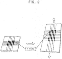
- FIG. 2 is a diagram for describing an example in which a distance between pixels included in a stretchable display panel driven by the gate driver of FIG. 1 and a size of each of the pixels are changed as the stretchable display panel is stretched.
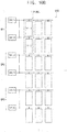
- FIG. 3 is a diagram illustrating an internal structure of the gate driver of FIG. 1 when a stretchable display panel is stretched.
- FIG. 4 is a diagram illustrating an internal structure of the gate driver of FIG. 1 when a stretchable display panel is not stretched.
- the gate driver 100 may include first through (i)th shift registers 120(1) through 120(i), where i is an integer greater than or equal to 2, and first through (j)th connection control blocks 140(1) through 140(j), where j is an integer greater than or equal to 2.
- the gate driver 100 may provide a gate signal to a stretchable display panel via first through (i)th gate lines GL(1) through GL(i).
- the gate driver 100 may provide a gate signal to the stretchable display panel via the first through (i)th gate lines GL(1) through GL(i) in response to a gate driving start signal STV input to the first shift register 120(1).
- the first through (i)th shift registers 120(1) through 120(i) may be connected to the first through (i)th gate lines GL(1) through GL(i) of the stretchable display panel, respectively.
- the first through (i)th shift registers 120(1) through 120(i) may be grouped into first through (j)th shift register groups 160(1) through 160(j).
- N shift registers that are adjacent to each other may constitute one shift register group 160(1) through 160(j), where N is an integer greater than or equal to 2.
- N is an integer greater than or equal to 2.
- the number (i.e., N) of shift registers 120(1) through 120(i) that constitute one shift register group 160(1) through 160(j) is not limited thereto.
- three or more adjacent shift registers 120(1) through 120(i) may constitute one shift register group 160(1) through 160(j).
- the first through (j)th shift register groups 160(1) through 160(j) may be connected in a cascade form (i.e., in a serial form).
- the first through (j)th shift register groups 160(1) through 160(j) may sequentially output the gate signal.
- the second shift register group 160(2) may output the gate signal after the first shift register group 160(1) outputs the gate signal
- the third shift register group 160(3) may output the gate signal after the second shift register group 160(2) outputs the gate signal
- the (j)th shift register group 160(j) may output the gate signal after the (j-1)th shift register group 160(j-1) outputs the gate signal.
- connecting the first through (j)th shift register groups 160(1) through 160(j) in a cascade form means arranging the first through (j)th shift register groups 160(1) through 160(j) to sequentially output the gate signal.
- two pixels i.e., an upper pixel and a lower pixel
- two shift registers 120(1) through 120(i) included in each of the first through (j)th shift register groups 160(1) through 160(j) may operate as one pixel (i.e., indicated by 1 PIXEL on the left side of FIG. 2 ).
- two pixels i.e., an upper pixel and a lower pixel
- the two shift registers 120(1) through 120(i) included in each of the first through (j)th shift register groups 160(1) through 160(j) may independently operate (i.e., indicated by 1 PIXEL on the right side of FIG. 2 ).
- the gate driver 100 may maintain the pixels-per-inch of the stretched panel region by controlling the two pixels connected to the two shift registers 120(1) through 120(i) included in each of the first through (j)th shift register groups 160(1) through 160(j) to operate as one pixel when the stretchable display panel is not stretched and by controlling the two pixels connected to the two shift registers 120(1) through 120(i) included in each of the first through (j)th shift register groups 160(1) through 160(j) to independently operate when the stretchable display panel is stretched.
- the first through (j)th connection control blocks 140(1) through 140(j) may connect the N shift registers 120(1) through 120(i) included in the (k)th shift register group 160(k) in a cascade form, where k is an integer between 1 and j, when a panel region connected to the (k)th shift register group 160(k) is stretched.
- the N shift registers 120(1) through 120(i) included in the (k)th shift register group 160(k) may sequentially output the gate signal via the first through (i)th gate lines GL(1) through GL(i).
- the first shift register 120(1) and the second shift register 120(2) included in the first shift register group 160(1) are connected in a cascade form as a panel region connected to the first shift register group 160(1) is stretched, an output of the first shift register 120(1) may be connected to an input of the second shift register 120(2).
- the second shift register 120(2) may output the gate signal via the second gate line GL(2).
- the third shift register 120(3) and the fourth shift register 120(4) included in the second shift register group 160(2) are connected in a cascade form as a panel region connected to the second shift register group 160(2) is stretched, an output of the third shift register 120(3) may be connected to an input of the fourth shift register 120(4).
- the fourth shift register 120(4) may output the gate signal via the fourth gate line GL(4).
- connecting the N shift registers 120(1) through 120(i) included in the (k)th shift register group 160(k) in a cascade form means arranging the N shift registers 120(1) through 120(i) included in the (k)th shift register group 160(k) to sequentially output the gate signal in the (k)th shift register group 160(k).
- the first through (j)th connection control blocks 140(1) through 140(j) may connect the N shift registers 120(1) through 120(i) included in the (k)th shift register group 160(k) in a parallel form when a panel region connected to the (k)th shift register group 160(k) is not stretched.
- the N shift registers 120(1) through 120(i) included in the (k)th shift register group 160(k) may simultaneously output the gate signal via the first through (i)th gate lines GL(1) through GL(i).
- the first shift register 120(1) and the second shift register 120(2) included in the first shift register group 160(1) are connected in a parallel form as a panel region connected to the first shift register group 160(1) is not stretched, an input of the first shift register 120(1) may be connected to an input of the second shift register 120(2).
- the first shift register 120(1) outputs the gate signal via the first gate line GL(1)
- the second shift register 120(2) may output the gate signal via the second gate line GL(2).
- the third shift register 120(3) and the fourth shift register 120(4) included in the second shift register group 160(2) are connected in a parallel form as a panel region connected to the second shift register group 160(2) is not stretched, an input of the third shift register 120(3) may be connected to an input of the fourth shift register 120(4).
- the fourth shift register 120(4) may output the gate signal via the fourth gate line GL(4).
- connecting the N shift registers 120(1) through 120(i) included in the (k)th shift register group 160(k) in a parallel form means arranging the N shift registers 120(1) through 120(i) included in the (k)th shift register group 160(k) to simultaneously output the gate signal in the (k)th shift register group 160(k).
- each of the first through (j)th connection control blocks 140(1) through 140(j) may include a plurality of switches that are turned on or off based on a stretch detection signal indicating whether the stretchable display panel is stretched.
- the stretch detection signal applied to the (k)th connection control block 140(k) may indicate that a panel region connected to the (k)th shift register group 160(k) is stretched when a distance between adjacent gate lines GL(1) through GL(i) in the panel region is longer than or equal to a reference distance and may indicate that a panel region connected to the (k)th shift register group 160(k) is not stretched when a distance between adjacent gate lines GL(1) through GL(i) in the panel region is shorter than the reference distance.
- the (k)th connection control block 140(k) in response to the stretch detection signal, may turn on the switches for connecting the N shift registers 120(1) through 120(i) included in the (k)th shift register group 160(k) in a cascade form and may turn off the switches for connecting the N shift registers 120(1) through 120(i) included in the (k)th shift register group 160(k) in a parallel form.
- the (k)th connection control block 140(k) when the stretch detection signal applied to the (k)th connection control block 140(k) indicates that the panel region connected to the (k)th shift register group 160(k) is not stretched, the (k)th connection control block 140(k), in response to the stretch detection signal, may turn on the switches for connecting the N shift registers 120(1) through 120(i) included in the (k)th shift register group 160(k) in a parallel form and may turn off the switches for connecting the N shift registers 120(1) through 120(i) included in the (k)th shift register group 160(k) in a cascade form.
- each of the switches included in each of the first through (j)th connection control blocks 140(1) through 140(j) may be implemented by a p-channel metal oxide semiconductor (PMOS) transistor, an n-channel metal oxide semiconductor (NMOS) transistor, or a complementary metal oxide semiconductor (CMOS) transistor.
- PMOS metal oxide semiconductor
- NMOS n-channel metal oxide semiconductor
- CMOS complementary metal oxide semiconductor
- a kind of the switches is not limited thereto.
- each of the first through (j)th connection control blocks 140(1) through 140(j) may include conductive connection lines that are physically (or electrically) connected or separated according to whether the stretchable display panel is stretched.
- the conductive connection lines for connecting the N shift registers 120(1) through 120(i) included in the (k)th shift register group 160(k) in a cascade form may be connected, and the conductive connection lines for connecting the N shift registers 120(1) through 120(i) included in the (k)th shift register group 160(k) in a parallel form may be separated.
- the conductive connection lines for connecting the N shift registers 120(1) through 120(i) included in the (k)th shift register group 160(k) in a parallel form may be connected, and the conductive connection lines for connecting the N shift registers 120(1) through 120(i) included in the (k)th shift register group 160(k) in a cascade form may be separated.
- the gate driver 100 may maintain the pixels-per-inch of a stretched panel region of the stretchable display panel when the stretchable display panel is stretched by grouping adjacent shift registers 120(1) through 120(i) into shift register groups 160(1) through 160(j), by arranging the N shift registers 120(1) through 120(i) included in each of the shift register groups 160(1) through 160(j) in a cascade form when the stretchable display panel is stretched, and by arranging the N shift registers 120(1) through 120(i) included in each of the shift register groups 160(1) through 160(j) in a parallel form when the stretchable display panel is not stretched.
- all of the shift registers in the shift register groups illustrated in FIGS. 3 and 4 are connected in the same manner, it is to be understood that different ones of the shift registers within the shift register groups may be controlled depending on the degree of stretching within that shift register group, i.e., may be different for different shift register groups.
- FIG. 5 is a flowchart illustrating an example in which an internal structure of the gate driver of FIG. 1 is changed.
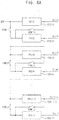
- FIGS. 6A and 6B are diagrams for describing an example in which an internal structure of the gate driver of FIG. 1 is changed based on a turn-on operation or a turn-off operation of switches.
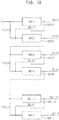
- FIGS. 7A and 7B are diagrams for describing an example in which an internal structure of the gate driver of FIG. 1 is changed based on a physical connection or a physical separation of conductive connecting lines.
- the gate driver 100 may compare a distance between adjacent gate lines GL(1) through GL(i) of the stretchable display panel with a reference distance (S120) and may check whether the distance between the adjacent gate lines GL(1) through GL(i) of the stretchable display panel is longer than or equal to the reference distance (S140).
- the gate driver 100 may connect the shift registers 120(1) through 120(i) included in the shift register group connected to the first panel region in a cascade form (S160).
- the shift registers 120(1) through 120(i) included in the shift register group connected to the first panel region of the stretchable display panel may sequentially output the gate signal via the gate lines GL(1) through GL(i).
- the pixels i.e., an upper pixel and a lower pixel located in the first panel region of the stretchable display panel may independently operate because the pixels located in the first panel region of the stretchable display panel independently (i.e., sequentially) receive the gate signal.
- the gate driver 100 may connect the shift registers 120(1) through 120(i) included in the shift register group connected to the second panel region in a parallel form (S180).
- the shift registers 120(1) through 120(i) included in the shift register group connected to the second panel region of the stretchable display panel may simultaneously output the gate signal via the gate lines GL(1) through GL(i).
- the pixels i.e., an upper pixel and a lower pixel located in the second panel region of the stretchable display panel may operate as one pixel because the pixels located in the second panel region of the stretchable display panel simultaneously receive the gate signal.
- the gate driver 100 may maintain the pixels-per-inch (PPI) of a stretched panel region of the stretchable display panel even when the stretchable display panel is stretched.
- PPI pixels-per-inch
- FIG. 5 illustrates an operation S180 to connect shift registers in a shift register group in parallel
- the operation of the display may set all shift registers in a corresponding shift register group in parallel as a default setting, such that no action is required when the distance is shorter than the reference distance.
- each of the first through (j)th connection control blocks may include a first switch FSW(1) through FSW(j) for connecting two shift registers 120(1) through 120(i) included in each shift register group in a parallel form and a second switch SSW(1) through SSW(j) for connecting two shift registers 120(1) through 120(i) included in each shift register group in a cascade form.
- the first switch FSW(1) through FSW(j) and the second switch SSW(1) through SSW(j) may be turned on or off based on the stretch detection signal.
- the first switch FSW(1) through FSW(j) for connecting two shift registers 120(1) through 120(i) included in each shift register group in a parallel form may be turned on, and the second switch SSW(1) through SSW(j) for connecting two shift registers 120(1) through 120(i) included in each shift register group in a cascade form may be turned off.
- two shift registers 120(1) through 120(i) included in each shift register group may simultaneously output the gate signal via the gate lines GL(1) through GL(i), and two pixels (i.e., an upper pixel and a lower pixel) connected to each shift register group may operate as one pixel because the gate signal is simultaneously applied to the two pixels.
- a first stretch detection signal applied to the first switch FSW(1) through FSW(j) may have a logic 'high' level.
- the first switch FSW(1) through FSW(j) is implemented by an p-channel metal oxide semiconductor (PMOS) transistor
- the first stretch detection signal applied to the first switch FSW(1) through FSW(j) may have a logic 'low' level.
- the second switch SSW(1) through SSW(j) is implemented by an NMOS transistor
- a second stretch detection signal applied to the second switch SSW(1) through SSW(j) may have a logic 'low' level.
- the second stretch detection signal applied to the second switch SSW(1) through SSW(j) may have a logic 'high' level.
- the first switch FSW(1) through FSW(j) for connecting two shift registers 120(1) through 120(i) included in each shift register group in a parallel form may be turned off, and the second switch SSW(1) through SSW(j) for connecting two shift registers 120(1) through 120(i) included in each shift register group in a cascade form may be turned on.
- two shift registers 120(1) through 120(i) included in each shift register group may sequentially output the gate signal via the gate lines GL(1) through GL(i), and two pixels (i.e., an upper pixel and a lower pixel) connected to each shift register group may independently operate because the gate signal is independently (i.e., sequentially) applied to the two pixels.
- a first stretch detection signal applied to the first switch FSW(1) through FSW(j) may have a logic 'low' level.
- the first stretch detection signal applied to the first switch FSW(1) through FSW(j) may have a logic 'high' level.
- a second stretch detection signal applied to the second switch SSW(1) through SSW(j) may have a logic 'high' level.
- the second stretch detection signal applied to the second switch SSW(1) through SSW(j) may have a logic 'low' level.
- each of the first through (j)th connection control blocks may include a first conductive connecting line FCL(1) through FCL(j) for connecting two shift registers 120(1) through 120(i) included in each shift register group in a parallel form and a second conductive connecting line SCL(1) through SCL(j) for connecting two shift registers 120(1) through 120(i) included in each shift register group in a cascade form.
- the first conductive connecting line FCL(1) through FCL(j) and the second conductive connecting line SCL(1) through SCL(j) may be physically (or, electrically) connected or separated as the gate driver 100 is stretched when the stretchable display panel is stretched.
- the first conductive connecting line FCL(1) through FCL(j) for connecting two shift registers 120(1) through 120(i) included in each shift register group in a parallel form may be physically connected, and the second conductive connecting line SCL(1) through SCL(j) for connecting two shift registers 120(1) through 120(i) included in each shift register group in a cascade form may be physically separated.
- two shift registers 120(1) through 120(i) included in each shift register group may simultaneously output the gate signal via the gate lines GL(1) through GL(i), and two pixels (i.e., an upper pixel and a lower pixel) connected to each shift register group may operate as one pixel because the gate signal is simultaneously applied to the two pixels.
- the first conductive connecting line FCL(1) through FCL(j) for connecting two shift registers 120(1) through 120(i) included in each shift register group in a parallel form may be physically separated, and the second conductive connecting line SCL(1) through SCL(j) for connecting two shift registers 120(1) through 120(i) included in each shift register group in a cascade form may be physically (electrically) connected.
- two shift registers 120(1) through 120(i) included in each shift register group may sequentially output the gate signal via the gate lines GL(1) through GL(i), and two pixels (i.e., an upper pixel and a lower pixel) connected to each shift register group may independently operate because the gate signal is independently (i.e., sequentially) applied to the two pixels.
- each shift register group includes two shift registers 120(1) through 120(i)
- the number of the shift registers 120(1) through 120(i) included in each shift register group is not limited thereto.
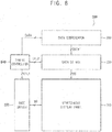
- FIG. 8 is a block diagram illustrating a display device according to example embodiments.
- FIG. 9 is a flowchart illustrating an example in which the display device of FIG. 8 operates.
- FIGS. 10A and 10B are diagrams for describing an example in which the display device of FIG. 8 operates.
- the display device 500 may include a stretchable display panel 510, a gate driver 520, a data driver 530, and a timing controller 540.
- the display device 500 may further include a data compensator 550 that performs luminance compensation according to whether the stretchable display panel 510 is stretched.
- the display device 500 may be an organic light emitting display (OLED) device or a liquid crystal display (LCD) device.
- OLED organic light emitting display
- LCD liquid crystal display
- the stretchable display panel 510 may have elasticity and flexibility. Thus, a size (or, area) of the stretchable display panel 510 may be changed based on its elasticity and flexibility.
- the stretchable display panel 510 includes a flexible display panel, a bendable display panel, etc.
- the stretchable display panel 510 may include a plurality of pixels. In the stretchable display panel 510, the pixels may be arranged in a matrix form at locations corresponding to intersecting points of gate lines and data lines. Thus, when the display device 500 includes A gate lines and B data lines, the number of the pixels included in the stretchable display panel 510 may be A ⁇ B.
- the stretchable display panel 510 may be connected to the gate driver 520 via the gate lines.
- the stretchable display panel 510 may be connected to the data driver 530 via the data lines.
- the data lines since the stretchable display panel 510 is stretched in a up-and-down direction (i.e., in a direction in which the data lines extend), the data lines may have a spring structure in order that the data lines are stretched as the stretchable display panel 510 is stretched. That is, the spring structure of the data lines may prevent the data lines from being cut when the stretchable display panel 510 is stretched.
- the gate lines may also have a spring structure in order that the gate lines are stretched as the stretchable display panel 510 is stretched. That is, the spring structure of the gate lines may prevent the gate lines from being cut when the stretchable display panel 510 is stretched.
- the gate driver 520 may provide a gate signal SS to the stretchable display panel 510 via the gate lines.
- the data driver 530 may provide a data signal DS corresponding to image data DATA to the stretchable display panel 510 via the data lines.
- the display device 500 may further include the data compensator 550.
- the data driver 530 may provide a data signal DS corresponding to compensated image data DATA' to the stretchable display panel 510 via the data lines.
- the timing controller 540 may control the gate driver 520 and the data driver 530.
- the timing controller 540 may generate control signals CTL1 and CTL2 to provide the control signals CTL1 and CTL2 to the gate driver 520 and the data driver 530, respectively.
- pixels P1-1 and P1-2 included in the stretchable display panel 510 may also be stretched. That is, a pixels-per-inch of a stretched panel region of the stretchable display panel 510 may be decreased.
- the pixels P1-1 and P1-2 included in the stretchable display panel 510 may operate as one pixel or may independently operate according to whether the stretchable display panel 510 is stretched. As a result, the pixels-per-inch of the stretched panel region of the stretchable display panel 510 may be maintained regardless of whether the stretchable display panel 510 is stretched.
- the pixels P1-1 and P1-2 when the stretchable display panel 510 is not stretched, the pixels P1-1 and P1-2 may operate as one pixel (i.e., indicated by 1 PIXEL). That is, the pixels P1-1 and P1-2 may simultaneously receive the gate signal SS from the gate driver 520, and thus the pixels P1-1 and P1-2 may operate as one pixel.
- the pixels P1-1 and P1-2 when the stretchable display panel 510 is stretched, the pixels P1-1 and P1-2 may independently (i.e., sequentially) operate (i.e., indicated by 1 PIXEL).
- the pixels P1-1 and P1-2 may sequentially receive the gate signal SS from the gate driver 520, and thus the pixels P1-1 and P1-2 may independently operate.
- the gate driver 520 may include a plurality of shift registers SR(1) through SR(6) and a plurality of connection control blocks (not shown).
- the shift registers SR(1) through SR(6) may be connected to the gate lines of the stretchable display panel 510, respectively.
- the shift registers SR(1) through SR(6) may be grouped into a plurality of shift register groups GP1 through GP3.
- N shift registers SR(1) through SR(6) may constitute each shift register group GP1 through GP3.
- each shift register group GP1 through GP3 may be connected to grouped pixels included in the stretchable display panel 510 (i.e., the pixels P1-1 and P1-2 illustrated in FIGS. 10A and 10B ) via the gate lines.
- the connection control blocks of the gate driver 520 may connect N shift registers (e.g., SR(1) and SR(2)) included in the (k)th shift register group (e.g., GP1) in a parallel form because a distance between the pixels P1-1 and P1-2 located in the panel region is not increased.
- N shift registers e.g., SR(1) and SR(2) included in the (k)th shift register group (e.g., GP1) may simultaneously output the gate signal SS via the gate lines.
- connection control blocks of the gate driver 520 may connect the N shift registers (e.g., SR(1) and SR(2)) included in the (k)th shift register group (e.g., GP1) in a cascade form because the distance between the pixels P1-1 and P1-2 located in the panel region is increased.
- the N shift registers (e.g., SR(1) and SR(2)) included in the (k)th shift register group (e.g., GP1) may independently (i.e., sequentially) output the gate signal SS via the gate lines. Since the shift register groups GP1 through GP3 are connected in a cascade form in the gate driver 520, the shift register groups GP1 through GP3 may sequentially output the gate signal SS regardless of whether the stretchable display panel 510 is stretched.
- the second shift register group GP2 may output the gate signal SS after the first shift register group GP1 outputs the gate signal SS
- the third shift register group GP3 may output the gate signal SS after the second shift register group GP2 outputs the gate signal SS.
- the N shift registers SR(1) through SR(6) included in each of the shift register groups GP1 through GP3 may simultaneously or sequentially output the gate signal SS according to whether the stretchable display panel 510 is stretched, and the shift register groups GP1 through GP3 may sequentially output the gate signal SS. Since these operations are described above, duplicated description will not be repeated.
- the display device 500 may further include the data compensator 550 that compensates for the image data DATA to output the compensated image data DATA' according to whether the stretchable display panel 510 is stretched. Specifically, as illustrated in FIG. 9 , when a panel region of the stretchable display panel 510 is stretched (S220), the display device 500 may check whether the pixels P1-1 and P1-2 included in the panel region of the stretchable display panel 510 are independently driven (S240).
- the display device 500 when the pixels P1-1 and P1-2 included in the panel region of the stretchable display panel 510 are independently driven, the display device 500, by using the data compensator 550, may compensate for the image data DATA corresponding to the data signal DS to be applied to the pixels P1-1 and P1-2 included in the panel region of the stretchable display panel 510 (S260). That is, the data compensator 550 of the display device 500 may perform the luminance compensation because luminance per unit area of the stretchable display panel 510 is reduced (or, degraded) when a distance between the pixels P1-1 and P1-2 included in the panel region of the stretchable display panel 510 is longer than or equal to a reference distance.
- the display device 500 may not compensate for the image data DATA corresponding to the data signal DS to be applied to the pixels P1-1 and P1-2 included in the panel region of the stretchable display panel 510 (S280). That is, the data compensator 550 of the display device 500 may not perform the luminance compensation when the distance between the pixels P1-1 and P1-2 included in the panel region of the stretchable display panel 510 is shorter than the reference distance.
- the data compensator 550 may be located outside the timing controller 540 and the data driver 530. In another example embodiment, the data compensator 550 may be located inside the timing controller 540 or the data driver 530.
- the display device 500 by using the gate driver 520 that maintains the pixels-per-inch of the stretched panel region of the stretchable display panel 510 when the stretchable display panel 510 is stretched, may prevent image distortion and luminance degradation of the stretchable display panel 510 when the stretchable display panel 510 is stretched. As a result, the display device 500 may provide a high-quality image to a viewer regardless of whether the stretchable display panel 510 is stretched.
- the display device 500 may further include other components.
- the display device 500 may further include a power supply that provides the stretchable display panel 510 with power voltages.
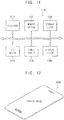
- FIG. 11 is a block diagram illustrating an electronic device according to example embodiments.
- FIG. 12 is a diagram illustrating an example in which the electronic device of FIG. 11 is implemented as a smart phone.
- the electronic device 1000 may include a processor 1010, a memory device 1020, a storage device 1030, an input/output (I/O) device 1040, a power supply 1050, and a display device 1060.
- the display device 1060 may correspond to a display device 500 of FIG. 8 .
- the electronic device 1000 may further include a plurality of ports for communicating a video card, a sound card, a memory card, a universal serial bus (USB) device, other electronic devices, etc.
- the electronic device 1000 may be implemented as a smart phone. However, the electronic device 1000 is not limited thereto.
- the electronic device 1000 may be implemented as a television, a computer monitor, a laptop, a digital camera, a cellular phone, a smart pad, a tablet PC, a navigation system, a video phone, a head mounted display (HMD), etc.
- a television a computer monitor, a laptop, a digital camera, a cellular phone, a smart pad, a tablet PC, a navigation system, a video phone, a head mounted display (HMD), etc.
- HMD head mounted display
- the processor 1010 may perform various computing functions.
- the processor 1010 may be a micro processor, a central processing unit (CPU), an application processor (AP), etc.
- the processor 1010 may be coupled to other components via an address bus, a control bus, a data bus, etc. Further, the processor 1010 may be coupled to an extended bus such as a peripheral component interconnection (PCI) bus.
- the memory device 1020 may store data for operations of the electronic device 1000.
- the memory device 1020 may include at least one non-volatile memory device such as an erasable programmable read-only memory (EPROM) device, an electrically erasable programmable read-only memory (EEPROM) device, a flash memory device, a phase change random access memory (PRAM) device, a resistance random access memory (RRAM) device, a nano floating gate memory (NFGM) device, a polymer random access memory (PoRAM) device, a magnetic random access memory (MRAM) device, a ferroelectric random access memory (FRAM) device, etc, and/or at least one volatile memory device such as a dynamic random access memory (DRAM) device, a static random access memory (SRAM) device, a mobile DRAM device, etc.
- EPROM erasable programmable read-only memory
- EEPROM electrically erasable programmable read-only memory
- flash memory device a phase change random access memory (PRAM) device, a resistance random access memory (RRAM) device, a nano floating gate
- the storage device 1030 may include a solid state drive (SSD) device, a hard disk drive (HDD) device, a CD-ROM device, etc.
- the I/O device 1040 may include an input device such as a keyboard, a keypad, a mouse device, a touchpad, a touch-screen, etc., and an output device such as a printer, a speaker, etc.
- the display device 1060 may be included in the I/O device 1040.
- the power supply 1050 may provide power for operations of the electronic device 1000.
- the display device 1060 may be coupled to other components via the buses or other communication links.
- the display device 1060 may be an organic light emitting display device or a liquid crystal display device.
- the display device 1060 is not limited thereto.
- the display device 1060 may include a stretchable display panel.
- the display device 1060 may provide a high-quality image to a viewer regardless of whether the stretchable display panel is stretched by preventing image distortion and luminance degradation of the stretchable display panel when the stretchable display panel is stretched.
- the display device 1060 may include the stretchable display panel that includes a plurality of pixels, a gate driver that provides a gate signal to the stretchable display panel via gate lines, a data driver that provides a data signal corresponding to image data to the stretchable display panel via data lines, and a timing controller that controls the gate driver and the data driver.
- the gate driver may include a plurality of shift registers and a plurality of connection control blocks.
- the shift registers may be connected to the gate lines of the stretchable display panel, respectively.
- the shift registers may be grouped into a plurality of shift register groups.
- N shift registers that are adjacent to each other may constitute one shift register group, where N is an integer greater than or equal to 2.
- the connection control blocks may change a connection structure of the N shift registers included in each of the shift register groups according to whether the stretchable display panel is stretched.
- the display device 1060 may further include a data compensator that compensates for the image data (i.e., compensates for the luminance degradation of the stretchable display panel) according to whether the stretchable display panel is stretched. In this case, the display device 1060, by using the data compensator, may prevent the luminance degradation that occurs when the stretchable display panel is stretched. Since the display device 1060 is described above, duplicated descriptions will not be repeated.
- the embodiments may be applied to a system (or, electronic device) including a display device.
- a system or, electronic device
- the present inventive concept may be applied to a television, a computer monitor, a head mounted display, a laptop, a digital camera, a cellular phone, a smart phone, a smart pad, a smart watch, a tablet PC, a navigation system, a video phone, etc.
- some example embodiments provide a gate driver capable of driving a stretchable display panel to maintain (or keep) a pixels-per-inch of a stretched panel region of the stretchable display panel when the stretchable display panel is stretched.
- Some example embodiments provide a display device including the gate driver capable of preventing image distortion and luminance degradation of the stretchable display panel when the stretchable display panel is stretched.
- a display device including the gate driver according to example embodiments may prevent (or alleviate, reduce, etc.) image distortion and luminance degradation of the stretchable display panel when the stretchable display panel is stretched.
Landscapes
- Engineering & Computer Science (AREA)
- Computer Hardware Design (AREA)
- Theoretical Computer Science (AREA)
- Physics & Mathematics (AREA)
- General Physics & Mathematics (AREA)
- Human Computer Interaction (AREA)
- General Engineering & Computer Science (AREA)
- Chemical & Material Sciences (AREA)
- Crystallography & Structural Chemistry (AREA)
- Control Of Indicators Other Than Cathode Ray Tubes (AREA)
- Liquid Crystal Display Device Control (AREA)
Abstract
Description
- Example embodiments relate generally to a display device. More particularly, embodiments of the present inventive concept relate to a gate driver that drives a stretchable display panel of which a size (or area) can be changed based on its elasticity and flexibility and a display device including the gate driver.
- A display device including a stretchable display panel (or, also referred to as a flexible display panel, a bendable display panel, etc.) allows a size (or area) of the stretchable display panel to be changed because the stretchable display panel has elasticity and flexibility. However, as the size of the stretchable display panel is changed based on its elasticity and flexibility, a distance (or space, gap, etc.) between pixels included in the stretchable display panel and a size of each of the pixels may be changed. For example, since the distance between the pixels and the size of each of the pixels increases as the stretchable display panel is stretched, a pixels-per-inch (PPI) (or pixel density) of a stretched panel region of the stretchable display panel may be decreased. Thus, in a conventional display device including the stretchable display panel, image distortion may occur (i.e., an image displayed on the stretchable display panel may be stretched as the stretchable display panel is stretched). In addition, luminance degradation may occur because the pixel density of the stretched panel region of the stretchable display panel is decreased.
- According to an aspect of example embodiments, a gate driver may include a plurality of shift registers connected to a plurality of gate lines of a stretchable display panel, respectively, the shift registers being grouped into a plurality of shift register groups, N adjacent shift registers constituting each of the shift register groups, where N is an integer greater than or equal to 2, and a plurality of connection controllers to change a connection structure of the N adjacent shift registers included in the each of the shift register groups according to whether the stretchable display panel is stretched.
- In example embodiments, the shift register groups may be connected in a cascade form to sequentially output a gate signal. When used herein, the term connected in a cascade form means a connection in series.
- In example embodiments, the connection controllers may connect the N adjacent shift registers included in the (k)th shift register group in a cascade form when a panel region connected to the (k)th shift register group is stretched, where k is an integer greater than or equal to 1.
- In example embodiments, the N adjacent shift registers included in the (k)th shift register group may sequentially output a gate signal via the gate lines when the panel region connected to the (k)th shift register group is stretched.
- In example embodiments, the connection controllers may connect the N adjacent shift registers included in the (k)th shift register group in a parallel form when a panel region connected to the (k)th shift register group is not stretched, where k is an integer greater than or equal to 1.
- In example embodiments, the N adjacent shift registers included in the (k)th shift register group may simultaneously output a gate signal via the gate lines when the panel region connected to the (k)th shift register group is not stretched.
- In example embodiments, each of the connection controllers may include a plurality of switches that are turned on or off based on a stretch detection signal indicating whether the stretchable display panel is stretched.
- In example embodiments, the stretch detection signal may indicate that a panel region connected to the (k)th shift register group is stretched when a distance between the gate lines included in the panel region connected to the (k)th shift register group is longer than or equal to a reference distance, where k is an integer greater than or equal to 1. In addition, the stretch detection signal may indicate that the panel region connected to the (k)th shift register group is not stretched when the distance between the gate lines included in the panel region connected to the (k)th shift register group is shorter than the reference distance.
- In example embodiments, each of the switches may be implemented by a p-channel metal oxide semiconductor (PMOS) transistor, an n-channel metal oxide semiconductor (NMOS) transistor, or a complementary metal oxide semiconductor (CMOS) transistor.
- In example embodiments, the gate driver may be stretched as the stretchable display panel is stretched.
- In example embodiments, each of the connection controllers may include a plurality of conductive connecting lines that are physically connected or separated according to whether the stretchable display panel is stretched.
- According to an aspect of example embodiments, a display device may include a stretchable display panel including a plurality of pixels, a gate driver configured to provide a gate signal to the stretchable display panel via a plurality of gate lines, a data driver configured to provide a data signal corresponding to image data to the stretchable display panel via a plurality of data lines, and a timing controller configured to control the gate driver and the data driver. Here, the gate driver may include a plurality of shift registers connected to the gate lines of the stretchable display panel, respectively, the shift registers being grouped into a plurality of shift register groups, N adjacent shift registers constituting each of the shift register groups, where N is an integer greater than or equal to 2, and a plurality of connection controllers to change a connection structure of the N adjacent shift registers included in the each of the shift register groups according to whether the stretchable display panel is stretched.
- In example embodiments, the display device may further include a data compensator configured to compensate for the image data according to whether the stretchable display panel is stretched.
- In example embodiments, the data compensator may be located inside the timing controller or the data driver.
- In example embodiments, the data compensator may be located outside the timing controller and the data driver.
- In example embodiments, the shift register groups may be connected in a cascade form to sequentially output the gate signal.
- In example embodiments, the connection controllers may connect the N adjacent shift registers included in the (k)th shift register group in a cascade form when a panel region connected to the (k)th shift register group is stretched, where k is an integer greater than or equal to 1.
- In example embodiments, the N adjacent shift registers included in the (k)th shift register group may sequentially output the gate signal via the gate lines when the panel region connected to the (k)th shift register group is stretched.
- In example embodiments, the connection controllers may connect the N adjacent shift registers included in the (k)th shift register group in a parallel form when a panel region connected to the (k)th shift register group is not stretched, where k is an integer greater than or equal to 1.
- In example embodiments, the N adjacent shift registers included in the (k)th shift register group may simultaneously output the gate signal via the gate lines when the panel region connected to the (k)th shift register group is not stretched.
- Therefore, a gate driver according to example embodiments may maintain a pixels-per-inch (PPI) of a stretched panel region of a stretchable display panel when the stretchable display panel is stretched by grouping adjacent shift registers into shift register groups, by arranging the shift registers included in each of the shift register groups in a cascade form when the stretchable display panel is stretched, and by arranging the shift registers included in each of the shift register groups in a parallel form when the stretchable display panel is not stretched.
- Features will become apparent to those of skill in the art by describing in detail exemplary embodiments with reference to the attached drawings in which:
-
FIG. 1 illustrates a block diagram of a gate driver according to example embodiments. -
FIG. 2 illustrates a diagram for describing an example in which a distance between pixels included in a stretchable display panel driven by the gate driver ofFIG. 1 and a size of each of the pixels are changed as the stretchable display panel is stretched. -
FIG. 3 illustrates a diagram of an internal structure of the gate driver ofFIG. 1 when a stretchable display panel is stretched. -
FIG. 4 illustrates a diagram of an internal structure of the gate driver ofFIG. 1 when a stretchable display panel is not stretched. -
FIG. 5 illustrates a flowchart illustrating an example in which an internal structure of the gate driver ofFIG. 1 is changed. -
FIGS. 6A and6B illustrate diagrams for describing an example in which an internal structure of the gate driver ofFIG. 1 is changed based on a turn-on operation or a turn-off operation of switches. -
FIGS. 7A and7B illustrate diagrams for describing an example in which an internal structure of the gate driver ofFIG. 1 is changed based on a physical connection or a physical separation of conductive connecting lines. -
FIG. 8 illustrates a block diagram of a display device according to example embodiments. -
FIG. 9 illustrates a flowchart of an example in which the display device ofFIG. 8 operates. -
FIGS. 10A and10B illustrate diagrams for describing an example in which the display device ofFIG. 8 operates. -
FIG. 11 illustrates a block diagram of an electronic device according to example embodiments. -
FIG. 12 illustrates a diagram of an example in which the electronic device ofFIG. 11 is implemented as a smart phone. - Example embodiments will now be described more fully hereinafter with reference to the accompanying drawings; however, they may be embodied in different forms and should not be construed as limited to the embodiments set forth herein. Rather, these embodiments are provided so that this disclosure will be thorough and complete, and will fully convey exemplary implementations to those skilled in the art.
-
FIG. 1 is a block diagram illustrating a gate driver according to example embodiments.FIG. 2 is a diagram for describing an example in which a distance between pixels included in a stretchable display panel driven by the gate driver ofFIG. 1 and a size of each of the pixels are changed as the stretchable display panel is stretched.FIG. 3 is a diagram illustrating an internal structure of the gate driver ofFIG. 1 when a stretchable display panel is stretched.FIG. 4 is a diagram illustrating an internal structure of the gate driver ofFIG. 1 when a stretchable display panel is not stretched. - Referring to
FIGS. 1 through 4 , thegate driver 100 may include first through (i)th shift registers 120(1) through 120(i), where i is an integer greater than or equal to 2, and first through (j)th connection control blocks 140(1) through 140(j), where j is an integer greater than or equal to 2. Here, thegate driver 100 may provide a gate signal to a stretchable display panel via first through (i)th gate lines GL(1) through GL(i). For example, thegate driver 100 may provide a gate signal to the stretchable display panel via the first through (i)th gate lines GL(1) through GL(i) in response to a gate driving start signal STV input to the first shift register 120(1). - The first through (i)th shift registers 120(1) through 120(i) may be connected to the first through (i)th gate lines GL(1) through GL(i) of the stretchable display panel, respectively. As illustrated in
FIG. 1 , the first through (i)th shift registers 120(1) through 120(i) may be grouped into first through (j)th shift register groups 160(1) through 160(j). Here, N shift registers that are adjacent to each other may constitute one shift register group 160(1) through 160(j), where N is an integer greater than or equal to 2. For convenience of description, although it is illustrated inFIGS. 1 through 4 that two adjacent shift registers 120(1) through 120(i) constitute one shift register group 160(1) through 160(j) (i.e., N=2), the number (i.e., N) of shift registers 120(1) through 120(i) that constitute one shift register group 160(1) through 160(j) is not limited thereto. For example, three or more adjacent shift registers 120(1) through 120(i) may constitute one shift register group 160(1) through 160(j). In example embodiments, the first through (j)th shift register groups 160(1) through 160(j) may be connected in a cascade form (i.e., in a serial form). Thus, the first through (j)th shift register groups 160(1) through 160(j) may sequentially output the gate signal. - Specifically, as illustrated in
FIG. 1 , since the first through (j)th shift register groups 160(1) through 160(j) are connected in a cascade form, the second shift register group 160(2) may output the gate signal after the first shift register group 160(1) outputs the gate signal, the third shift register group 160(3) may output the gate signal after the second shift register group 160(2) outputs the gate signal, and the (j)th shift register group 160(j) may output the gate signal after the (j-1)th shift register group 160(j-1) outputs the gate signal. In other words, connecting the first through (j)th shift register groups 160(1) through 160(j) in a cascade form means arranging the first through (j)th shift register groups 160(1) through 160(j) to sequentially output the gate signal. - The first through (j)th connection control blocks 140(1) through 140(j) may change a connection structure of the N shift registers 120(1) through 120(i) included in each of the first through (j)th shift register groups 160(1) through 160(j) according to whether the stretchable display panel is stretched. That is, as illustrated in
FIG. 2 , when the stretchable display panel is not stretched, two shift registers 120(1) through 120(i) (i.e., N=2) included in each of the first through (j)th shift register groups 160(1) through 160(j) may simultaneously output the gate signal. As a result, two pixels (i.e., an upper pixel and a lower pixel) connected to the two shift registers 120(1) through 120(i) included in each of the first through (j)th shift register groups 160(1) through 160(j) may operate as one pixel (i.e., indicated by 1 PIXEL on the left side ofFIG. 2 ). On the other hand, when the stretchable display panel is stretched, two shift registers 120(1) through 120(i) (i.e., N=2) included in each of the first through (j)th shift register groups 160(1) through 160(j) may sequentially output the gate signal. As a result, two pixels (i.e., an upper pixel and a lower pixel) connected to the two shift registers 120(1) through 120(i) included in each of the first through (j)th shift register groups 160(1) through 160(j) may independently operate (i.e., indicated by 1 PIXEL on the right side ofFIG. 2 ). - Generally, since a pixel included in the stretchable display panel is stretched as the stretchable display panel is stretched, a pixels-per-inch (or, pixel density) of a stretched panel region of the stretchable display panel may be decreased. Thus, the
gate driver 100 may maintain the pixels-per-inch of the stretched panel region by controlling the two pixels connected to the two shift registers 120(1) through 120(i) included in each of the first through (j)th shift register groups 160(1) through 160(j) to operate as one pixel when the stretchable display panel is not stretched and by controlling the two pixels connected to the two shift registers 120(1) through 120(i) included in each of the first through (j)th shift register groups 160(1) through 160(j) to independently operate when the stretchable display panel is stretched. - Specifically, the first through (j)th connection control blocks 140(1) through 140(j) may connect the N shift registers 120(1) through 120(i) included in the (k)th shift register group 160(k) in a cascade form, where k is an integer between 1 and j, when a panel region connected to the (k)th shift register group 160(k) is stretched. As a result, when the panel region connected to the (k)th shift register group 160(k) is stretched, the N shift registers 120(1) through 120(i) included in the (k)th shift register group 160(k) may sequentially output the gate signal via the first through (i)th gate lines GL(1) through GL(i).
- For example, as illustrated in
FIG. 3 , when the first shift register 120(1) and the second shift register 120(2) included in the first shift register group 160(1) are connected in a cascade form as a panel region connected to the first shift register group 160(1) is stretched, an output of the first shift register 120(1) may be connected to an input of the second shift register 120(2). Thus, after the first shift register 120(1) outputs the gate signal via the first gate line GL(1), the second shift register 120(2) may output the gate signal via the second gate line GL(2). In addition, when the third shift register 120(3) and the fourth shift register 120(4) included in the second shift register group 160(2) are connected in a cascade form as a panel region connected to the second shift register group 160(2) is stretched, an output of the third shift register 120(3) may be connected to an input of the fourth shift register 120(4). Thus, after the third shift register 120(3) outputs the gate signal via the third gate line GL(3), the fourth shift register 120(4) may output the gate signal via the fourth gate line GL(4). In other words, connecting the N shift registers 120(1) through 120(i) included in the (k)th shift register group 160(k) in a cascade form means arranging the N shift registers 120(1) through 120(i) included in the (k)th shift register group 160(k) to sequentially output the gate signal in the (k)th shift register group 160(k). - On the other hand, the first through (j)th connection control blocks 140(1) through 140(j) may connect the N shift registers 120(1) through 120(i) included in the (k)th shift register group 160(k) in a parallel form when a panel region connected to the (k)th shift register group 160(k) is not stretched. As a result, when the panel region connected to the (k)th shift register group 160(k) is not stretched, the N shift registers 120(1) through 120(i) included in the (k)th shift register group 160(k) may simultaneously output the gate signal via the first through (i)th gate lines GL(1) through GL(i).
- For example, as illustrated in
FIG. 4 , when the first shift register 120(1) and the second shift register 120(2) included in the first shift register group 160(1) are connected in a parallel form as a panel region connected to the first shift register group 160(1) is not stretched, an input of the first shift register 120(1) may be connected to an input of the second shift register 120(2). Thus, when the first shift register 120(1) outputs the gate signal via the first gate line GL(1), the second shift register 120(2) may output the gate signal via the second gate line GL(2). In addition, when the third shift register 120(3) and the fourth shift register 120(4) included in the second shift register group 160(2) are connected in a parallel form as a panel region connected to the second shift register group 160(2) is not stretched, an input of the third shift register 120(3) may be connected to an input of the fourth shift register 120(4). Thus, when the third shift register 120(3) outputs the gate signal via the third gate line GL(3), the fourth shift register 120(4) may output the gate signal via the fourth gate line GL(4). In other words, connecting the N shift registers 120(1) through 120(i) included in the (k)th shift register group 160(k) in a parallel form means arranging the N shift registers 120(1) through 120(i) included in the (k)th shift register group 160(k) to simultaneously output the gate signal in the (k)th shift register group 160(k). - In an example embodiment, each of the first through (j)th connection control blocks 140(1) through 140(j) may include a plurality of switches that are turned on or off based on a stretch detection signal indicating whether the stretchable display panel is stretched. Here, the stretch detection signal applied to the (k)th connection control block 140(k) may indicate that a panel region connected to the (k)th shift register group 160(k) is stretched when a distance between adjacent gate lines GL(1) through GL(i) in the panel region is longer than or equal to a reference distance and may indicate that a panel region connected to the (k)th shift register group 160(k) is not stretched when a distance between adjacent gate lines GL(1) through GL(i) in the panel region is shorter than the reference distance. Thus, when the stretch detection signal applied to the (k)th connection control block 140(k) indicates that the panel region connected to the (k)th shift register group 160(k) is stretched, the (k)th connection control block 140(k), in response to the stretch detection signal, may turn on the switches for connecting the N shift registers 120(1) through 120(i) included in the (k)th shift register group 160(k) in a cascade form and may turn off the switches for connecting the N shift registers 120(1) through 120(i) included in the (k)th shift register group 160(k) in a parallel form.
- On the other hand, when the stretch detection signal applied to the (k)th connection control block 140(k) indicates that the panel region connected to the (k)th shift register group 160(k) is not stretched, the (k)th connection control block 140(k), in response to the stretch detection signal, may turn on the switches for connecting the N shift registers 120(1) through 120(i) included in the (k)th shift register group 160(k) in a parallel form and may turn off the switches for connecting the N shift registers 120(1) through 120(i) included in the (k)th shift register group 160(k) in a cascade form. For example, each of the switches included in each of the first through (j)th connection control blocks 140(1) through 140(j) may be implemented by a p-channel metal oxide semiconductor (PMOS) transistor, an n-channel metal oxide semiconductor (NMOS) transistor, or a complementary metal oxide semiconductor (CMOS) transistor. However, a kind of the switches is not limited thereto.
- In another example embodiment, the
gate driver 100 may be stretched as the stretchable display panel is stretched. In this case, each of the first through (j)th connection control blocks 140(1) through 140(j) may include conductive connection lines that are physically (or electrically) connected or separated according to whether the stretchable display panel is stretched. For example, when a specific region of thegate driver 100 corresponding to the (k)th shift register group 160(k) is stretched as a panel region connected to the (k)th shift register group 160(k) is stretched, the conductive connection lines for connecting the N shift registers 120(1) through 120(i) included in the (k)th shift register group 160(k) in a cascade form may be connected, and the conductive connection lines for connecting the N shift registers 120(1) through 120(i) included in the (k)th shift register group 160(k) in a parallel form may be separated. - On the other hand, when a specific region of the
gate driver 100 corresponding to the (k)th shift register group 160(k) is not stretched as a panel region connected to the (k)th shift register group 160(k) is not stretched, the conductive connection lines for connecting the N shift registers 120(1) through 120(i) included in the (k)th shift register group 160(k) in a parallel form may be connected, and the conductive connection lines for connecting the N shift registers 120(1) through 120(i) included in the (k)th shift register group 160(k) in a cascade form may be separated. - In brief, the
gate driver 100 may maintain the pixels-per-inch of a stretched panel region of the stretchable display panel when the stretchable display panel is stretched by grouping adjacent shift registers 120(1) through 120(i) into shift register groups 160(1) through 160(j), by arranging the N shift registers 120(1) through 120(i) included in each of the shift register groups 160(1) through 160(j) in a cascade form when the stretchable display panel is stretched, and by arranging the N shift registers 120(1) through 120(i) included in each of the shift register groups 160(1) through 160(j) in a parallel form when the stretchable display panel is not stretched. Although all of the shift registers in the shift register groups illustrated inFIGS. 3 and4 are connected in the same manner, it is to be understood that different ones of the shift registers within the shift register groups may be controlled depending on the degree of stretching within that shift register group, i.e., may be different for different shift register groups. -
FIG. 5 is a flowchart illustrating an example in which an internal structure of the gate driver ofFIG. 1 is changed.FIGS. 6A and6B are diagrams for describing an example in which an internal structure of the gate driver ofFIG. 1 is changed based on a turn-on operation or a turn-off operation of switches.FIGS. 7A and7B are diagrams for describing an example in which an internal structure of the gate driver ofFIG. 1 is changed based on a physical connection or a physical separation of conductive connecting lines. - Referring to
FIGS. 5 through 7B , thegate driver 100 may compare a distance between adjacent gate lines GL(1) through GL(i) of the stretchable display panel with a reference distance (S120) and may check whether the distance between the adjacent gate lines GL(1) through GL(i) of the stretchable display panel is longer than or equal to the reference distance (S140). Here, when a first panel region in which the distance between the adjacent gate lines GL(1) through GL(i) of the stretchable display panel is greater than or equal to the reference distance exists, thegate driver 100 may connect the shift registers 120(1) through 120(i) included in the shift register group connected to the first panel region in a cascade form (S160). Thus, the shift registers 120(1) through 120(i) included in the shift register group connected to the first panel region of the stretchable display panel may sequentially output the gate signal via the gate lines GL(1) through GL(i). As a result, the pixels (i.e., an upper pixel and a lower pixel) located in the first panel region of the stretchable display panel may independently operate because the pixels located in the first panel region of the stretchable display panel independently (i.e., sequentially) receive the gate signal. In addition, when a second panel region in which the distance between adjacent gate lines GL(1) through GL(i) of the stretchable display panel is shorter than the reference distance exists, thegate driver 100 may connect the shift registers 120(1) through 120(i) included in the shift register group connected to the second panel region in a parallel form (S180). - Thus, the shift registers 120(1) through 120(i) included in the shift register group connected to the second panel region of the stretchable display panel may simultaneously output the gate signal via the gate lines GL(1) through GL(i). As a result, the pixels (i.e., an upper pixel and a lower pixel) located in the second panel region of the stretchable display panel may operate as one pixel because the pixels located in the second panel region of the stretchable display panel simultaneously receive the gate signal. As described above, since an internal structure of the
gate driver 100 differs according to whether the stretchable display panel is stretched (i.e., the shift registers 120(1) through 120(i) included in each shift register group are connected in a cascade form or in a parallel form), thegate driver 100 may maintain the pixels-per-inch (PPI) of a stretched panel region of the stretchable display panel even when the stretchable display panel is stretched. - Although
FIG. 5 illustrates an operation S180 to connect shift registers in a shift register group in parallel, the operation of the display may set all shift registers in a corresponding shift register group in parallel as a default setting, such that no action is required when the distance is shorter than the reference distance. - In an example embodiment, as illustrated in
FIGS. 6A and6B , each of the first through (j)th connection control blocks may include a first switch FSW(1) through FSW(j) for connecting two shift registers 120(1) through 120(i) included in each shift register group in a parallel form and a second switch SSW(1) through SSW(j) for connecting two shift registers 120(1) through 120(i) included in each shift register group in a cascade form. Here, the first switch FSW(1) through FSW(j) and the second switch SSW(1) through SSW(j) may be turned on or off based on the stretch detection signal. - For example, as illustrated in
FIG. 6A , if no panel region of the stretchable display panel is stretched, the first switch FSW(1) through FSW(j) for connecting two shift registers 120(1) through 120(i) included in each shift register group in a parallel form may be turned on, and the second switch SSW(1) through SSW(j) for connecting two shift registers 120(1) through 120(i) included in each shift register group in a cascade form may be turned off. Thus, two shift registers 120(1) through 120(i) included in each shift register group may simultaneously output the gate signal via the gate lines GL(1) through GL(i), and two pixels (i.e., an upper pixel and a lower pixel) connected to each shift register group may operate as one pixel because the gate signal is simultaneously applied to the two pixels. - When the first switch FSW(1) through FSW(j) is implemented by an n-channel metal oxide semiconductor (NMOS) transistor, a first stretch detection signal applied to the first switch FSW(1) through FSW(j) may have a logic 'high' level. When the first switch FSW(1) through FSW(j) is implemented by an p-channel metal oxide semiconductor (PMOS) transistor, the first stretch detection signal applied to the first switch FSW(1) through FSW(j) may have a logic 'low' level. When the second switch SSW(1) through SSW(j) is implemented by an NMOS transistor, a second stretch detection signal applied to the second switch SSW(1) through SSW(j) may have a logic 'low' level. When the second switch SSW(1) through SSW(j) is implemented by a PMOS transistor, the second stretch detection signal applied to the second switch SSW(1) through SSW(j) may have a logic 'high' level.
- On the other hand, as illustrated in
FIG. 6B , if all panel regions of the stretchable display panel are stretched, the first switch FSW(1) through FSW(j) for connecting two shift registers 120(1) through 120(i) included in each shift register group in a parallel form may be turned off, and the second switch SSW(1) through SSW(j) for connecting two shift registers 120(1) through 120(i) included in each shift register group in a cascade form may be turned on. Thus, two shift registers 120(1) through 120(i) included in each shift register group may sequentially output the gate signal via the gate lines GL(1) through GL(i), and two pixels (i.e., an upper pixel and a lower pixel) connected to each shift register group may independently operate because the gate signal is independently (i.e., sequentially) applied to the two pixels. When the first switch FSW(1) through FSW(j) is implemented by an NMOS transistor, a first stretch detection signal applied to the first switch FSW(1) through FSW(j) may have a logic 'low' level. When the first switch FSW(1) through FSW(j) is implemented by a PMOS transistor, the first stretch detection signal applied to the first switch FSW(1) through FSW(j) may have a logic 'high' level. - When the second switch SSW(1) through SSW(j) is implemented by an NMOS transistor, a second stretch detection signal applied to the second switch SSW(1) through SSW(j) may have a logic 'high' level. When the second switch SSW(1) through SSW(j) is implemented by a PMOS transistor, the second stretch detection signal applied to the second switch SSW(1) through SSW(j) may have a logic 'low' level.
- In another example embodiment, as illustrated in
FIGS. 7A and7B , each of the first through (j)th connection control blocks may include a first conductive connecting line FCL(1) through FCL(j) for connecting two shift registers 120(1) through 120(i) included in each shift register group in a parallel form and a second conductive connecting line SCL(1) through SCL(j) for connecting two shift registers 120(1) through 120(i) included in each shift register group in a cascade form. Here, the first conductive connecting line FCL(1) through FCL(j) and the second conductive connecting line SCL(1) through SCL(j) may be physically (or, electrically) connected or separated as thegate driver 100 is stretched when the stretchable display panel is stretched. - For example, as illustrated in
FIG. 7A , if no panel region of the stretchable display panel is stretched, the first conductive connecting line FCL(1) through FCL(j) for connecting two shift registers 120(1) through 120(i) included in each shift register group in a parallel form may be physically connected, and the second conductive connecting line SCL(1) through SCL(j) for connecting two shift registers 120(1) through 120(i) included in each shift register group in a cascade form may be physically separated. Thus, two shift registers 120(1) through 120(i) included in each shift register group may simultaneously output the gate signal via the gate lines GL(1) through GL(i), and two pixels (i.e., an upper pixel and a lower pixel) connected to each shift register group may operate as one pixel because the gate signal is simultaneously applied to the two pixels. - On the other hand, as illustrated in
FIG. 7B , if all panel regions of the stretchable display panel are stretched, the first conductive connecting line FCL(1) through FCL(j) for connecting two shift registers 120(1) through 120(i) included in each shift register group in a parallel form may be physically separated, and the second conductive connecting line SCL(1) through SCL(j) for connecting two shift registers 120(1) through 120(i) included in each shift register group in a cascade form may be physically (electrically) connected. Thus, two shift registers 120(1) through 120(i) included in each shift register group may sequentially output the gate signal via the gate lines GL(1) through GL(i), and two pixels (i.e., an upper pixel and a lower pixel) connected to each shift register group may independently operate because the gate signal is independently (i.e., sequentially) applied to the two pixels. Although it is illustrated inFIGS. 6A through 7B that each shift register group includes two shift registers 120(1) through 120(i), the number of the shift registers 120(1) through 120(i) included in each shift register group is not limited thereto. -
FIG. 8 is a block diagram illustrating a display device according to example embodiments.FIG. 9 is a flowchart illustrating an example in which the display device ofFIG. 8 operates.FIGS. 10A and10B are diagrams for describing an example in which the display device ofFIG. 8 operates. - Referring to
FIGS. 8 through 10B , thedisplay device 500 may include astretchable display panel 510, agate driver 520, adata driver 530, and atiming controller 540. In some example embodiments, thedisplay device 500 may further include adata compensator 550 that performs luminance compensation according to whether thestretchable display panel 510 is stretched. For example, thedisplay device 500 may be an organic light emitting display (OLED) device or a liquid crystal display (LCD) device. However, thedisplay device 500 is not limited thereto. - The
stretchable display panel 510 may have elasticity and flexibility. Thus, a size (or, area) of thestretchable display panel 510 may be changed based on its elasticity and flexibility. Here, it should be understood that thestretchable display panel 510 includes a flexible display panel, a bendable display panel, etc. Thestretchable display panel 510 may include a plurality of pixels. In thestretchable display panel 510, the pixels may be arranged in a matrix form at locations corresponding to intersecting points of gate lines and data lines. Thus, when thedisplay device 500 includes A gate lines and B data lines, the number of the pixels included in thestretchable display panel 510 may be A×B. Thestretchable display panel 510 may be connected to thegate driver 520 via the gate lines. Thestretchable display panel 510 may be connected to thedata driver 530 via the data lines. Here, since thestretchable display panel 510 is stretched in a up-and-down direction (i.e., in a direction in which the data lines extend), the data lines may have a spring structure in order that the data lines are stretched as thestretchable display panel 510 is stretched. That is, the spring structure of the data lines may prevent the data lines from being cut when thestretchable display panel 510 is stretched. - In some example embodiments, if the
stretchable display panel 510 can be stretched in a left-and-right direction (i.e., in a direction in which the gate lines extend), the gate lines may also have a spring structure in order that the gate lines are stretched as thestretchable display panel 510 is stretched. That is, the spring structure of the gate lines may prevent the gate lines from being cut when thestretchable display panel 510 is stretched. Thegate driver 520 may provide a gate signal SS to thestretchable display panel 510 via the gate lines. Thedata driver 530 may provide a data signal DS corresponding to image data DATA to thestretchable display panel 510 via the data lines. In some example embodiments, thedisplay device 500 may further include thedata compensator 550. In this case, thedata driver 530 may provide a data signal DS corresponding to compensated image data DATA' to thestretchable display panel 510 via the data lines. Thetiming controller 540 may control thegate driver 520 and thedata driver 530. Thus, thetiming controller 540 may generate control signals CTL1 and CTL2 to provide the control signals CTL1 and CTL2 to thegate driver 520 and thedata driver 530, respectively. - As illustrated in
FIGS. 10A and10B , when thestretchable display panel 510 is stretched, pixels P1-1 and P1-2 included in thestretchable display panel 510 may also be stretched. That is, a pixels-per-inch of a stretched panel region of thestretchable display panel 510 may be decreased. Thus, the pixels P1-1 and P1-2 included in thestretchable display panel 510 may operate as one pixel or may independently operate according to whether thestretchable display panel 510 is stretched. As a result, the pixels-per-inch of the stretched panel region of thestretchable display panel 510 may be maintained regardless of whether thestretchable display panel 510 is stretched. - For example, as illustrated in
FIG. 10A , when thestretchable display panel 510 is not stretched, the pixels P1-1 and P1-2 may operate as one pixel (i.e., indicated by 1 PIXEL). That is, the pixels P1-1 and P1-2 may simultaneously receive the gate signal SS from thegate driver 520, and thus the pixels P1-1 and P1-2 may operate as one pixel. On the other hand, as illustrated inFIG. 10B , when thestretchable display panel 510 is stretched, the pixels P1-1 and P1-2 may independently (i.e., sequentially) operate (i.e., indicated by 1 PIXEL). That is, the pixels P1-1 and P1-2 may sequentially receive the gate signal SS from thegate driver 520, and thus the pixels P1-1 and P1-2 may independently operate. For this operation, thegate driver 520 may include a plurality of shift registers SR(1) through SR(6) and a plurality of connection control blocks (not shown). The shift registers SR(1) through SR(6) may be connected to the gate lines of thestretchable display panel 510, respectively. In addition, the shift registers SR(1) through SR(6) may be grouped into a plurality of shift register groups GP1 through GP3. Here, N shift registers SR(1) through SR(6) may constitute each shift register group GP1 through GP3. - For example, it is illustrated in
FIGS. 10A and10B that two shift registers SR(1) through SR(6) constitutes each shift register group GP1 through GP3. The connection control blocks may change a connection structure of the N shift registers SR(1) through SR(6) included in each of the shift register groups GP1 through GP3 according to whether thestretchable display panel 510 is stretched. Here, each of the shift register groups GP1 through GP3 may be connected to grouped pixels included in the stretchable display panel 510 (i.e., the pixels P1-1 and P1-2 illustrated inFIGS. 10A and10B ) via the gate lines. - Specifically, when a panel region connected to a (k)th shift register group (e.g., GP1) is not stretched, the connection control blocks of the
gate driver 520 may connect N shift registers (e.g., SR(1) and SR(2)) included in the (k)th shift register group (e.g., GP1) in a parallel form because a distance between the pixels P1-1 and P1-2 located in the panel region is not increased. Thus, as illustrated inFIG. 10A , the N shift registers (e.g., SR(1) and SR(2)) included in the (k)th shift register group (e.g., GP1) may simultaneously output the gate signal SS via the gate lines. On the other hand, when the panel region connected to the (k)th shift register group (e.g., GP1) is stretched, the connection control blocks of thegate driver 520 may connect the N shift registers (e.g., SR(1) and SR(2)) included in the (k)th shift register group (e.g., GP1) in a cascade form because the distance between the pixels P1-1 and P1-2 located in the panel region is increased. - Thus, as illustrated in
FIG. 10B , the N shift registers (e.g., SR(1) and SR(2)) included in the (k)th shift register group (e.g., GP1) may independently (i.e., sequentially) output the gate signal SS via the gate lines. Since the shift register groups GP1 through GP3 are connected in a cascade form in thegate driver 520, the shift register groups GP1 through GP3 may sequentially output the gate signal SS regardless of whether thestretchable display panel 510 is stretched. For example, the second shift register group GP2 may output the gate signal SS after the first shift register group GP1 outputs the gate signal SS, and the third shift register group GP3 may output the gate signal SS after the second shift register group GP2 outputs the gate signal SS. In brief, as illustrated inFIGS. 10A and10B , the N shift registers SR(1) through SR(6) included in each of the shift register groups GP1 through GP3 may simultaneously or sequentially output the gate signal SS according to whether thestretchable display panel 510 is stretched, and the shift register groups GP1 through GP3 may sequentially output the gate signal SS. Since these operations are described above, duplicated description will not be repeated. - In some example embodiments, the
display device 500 may further include the data compensator 550 that compensates for the image data DATA to output the compensated image data DATA' according to whether thestretchable display panel 510 is stretched. Specifically, as illustrated inFIG. 9 , when a panel region of thestretchable display panel 510 is stretched (S220), thedisplay device 500 may check whether the pixels P1-1 and P1-2 included in the panel region of thestretchable display panel 510 are independently driven (S240). - Here, as illustrated in
FIG. 10B , when the pixels P1-1 and P1-2 included in the panel region of thestretchable display panel 510 are independently driven, thedisplay device 500, by using the data compensator 550, may compensate for the image data DATA corresponding to the data signal DS to be applied to the pixels P1-1 and P1-2 included in the panel region of the stretchable display panel 510 (S260). That is, the data compensator 550 of thedisplay device 500 may perform the luminance compensation because luminance per unit area of thestretchable display panel 510 is reduced (or, degraded) when a distance between the pixels P1-1 and P1-2 included in the panel region of thestretchable display panel 510 is longer than or equal to a reference distance. - On the other hand, as illustrated in
FIG. 10A , when the pixels P1-1 and P1-2 included in the panel region of thestretchable display panel 510 are not independently driven, thedisplay device 500 may not compensate for the image data DATA corresponding to the data signal DS to be applied to the pixels P1-1 and P1-2 included in the panel region of the stretchable display panel 510 (S280). That is, the data compensator 550 of thedisplay device 500 may not perform the luminance compensation when the distance between the pixels P1-1 and P1-2 included in the panel region of thestretchable display panel 510 is shorter than the reference distance. - In an example embodiment, as illustrated in
FIG. 8 , the data compensator 550 may be located outside thetiming controller 540 and thedata driver 530. In another example embodiment, the data compensator 550 may be located inside thetiming controller 540 or thedata driver 530. As described above, thedisplay device 500, by using thegate driver 520 that maintains the pixels-per-inch of the stretched panel region of thestretchable display panel 510 when thestretchable display panel 510 is stretched, may prevent image distortion and luminance degradation of thestretchable display panel 510 when thestretchable display panel 510 is stretched. As a result, thedisplay device 500 may provide a high-quality image to a viewer regardless of whether thestretchable display panel 510 is stretched. Although it is described above that thedisplay device 500 includes thestretchable display panel 510, thegate driver 520, thedata driver 530, thetiming controller 540, and/or the data compensator 550, thedisplay device 500 may further include other components. For example, thedisplay device 500 may further include a power supply that provides thestretchable display panel 510 with power voltages. -
FIG. 11 is a block diagram illustrating an electronic device according to example embodiments.FIG. 12 is a diagram illustrating an example in which the electronic device ofFIG. 11 is implemented as a smart phone. - Referring to
FIGS. 11 and 12 , theelectronic device 1000 may include aprocessor 1010, amemory device 1020, astorage device 1030, an input/output (I/O)device 1040, apower supply 1050, and adisplay device 1060. Here, thedisplay device 1060 may correspond to adisplay device 500 ofFIG. 8 . In addition, theelectronic device 1000 may further include a plurality of ports for communicating a video card, a sound card, a memory card, a universal serial bus (USB) device, other electronic devices, etc. In an example embodiment, as illustrated inFIG. 12 , theelectronic device 1000 may be implemented as a smart phone. However, theelectronic device 1000 is not limited thereto. For example, theelectronic device 1000 may be implemented as a television, a computer monitor, a laptop, a digital camera, a cellular phone, a smart pad, a tablet PC, a navigation system, a video phone, a head mounted display (HMD), etc. - The
processor 1010 may perform various computing functions. Theprocessor 1010 may be a micro processor, a central processing unit (CPU), an application processor (AP), etc. Theprocessor 1010 may be coupled to other components via an address bus, a control bus, a data bus, etc. Further, theprocessor 1010 may be coupled to an extended bus such as a peripheral component interconnection (PCI) bus. Thememory device 1020 may store data for operations of theelectronic device 1000. For example, thememory device 1020 may include at least one non-volatile memory device such as an erasable programmable read-only memory (EPROM) device, an electrically erasable programmable read-only memory (EEPROM) device, a flash memory device, a phase change random access memory (PRAM) device, a resistance random access memory (RRAM) device, a nano floating gate memory (NFGM) device, a polymer random access memory (PoRAM) device, a magnetic random access memory (MRAM) device, a ferroelectric random access memory (FRAM) device, etc, and/or at least one volatile memory device such as a dynamic random access memory (DRAM) device, a static random access memory (SRAM) device, a mobile DRAM device, etc. Thestorage device 1030 may include a solid state drive (SSD) device, a hard disk drive (HDD) device, a CD-ROM device, etc. The I/O device 1040 may include an input device such as a keyboard, a keypad, a mouse device, a touchpad, a touch-screen, etc., and an output device such as a printer, a speaker, etc. In some example embodiments, thedisplay device 1060 may be included in the I/O device 1040. Thepower supply 1050 may provide power for operations of theelectronic device 1000. - The
display device 1060 may be coupled to other components via the buses or other communication links. In an example embodiment, thedisplay device 1060 may be an organic light emitting display device or a liquid crystal display device. However, thedisplay device 1060 is not limited thereto. As described above, thedisplay device 1060 may include a stretchable display panel. Here, thedisplay device 1060 may provide a high-quality image to a viewer regardless of whether the stretchable display panel is stretched by preventing image distortion and luminance degradation of the stretchable display panel when the stretchable display panel is stretched. To this end, thedisplay device 1060 may include the stretchable display panel that includes a plurality of pixels, a gate driver that provides a gate signal to the stretchable display panel via gate lines, a data driver that provides a data signal corresponding to image data to the stretchable display panel via data lines, and a timing controller that controls the gate driver and the data driver. - In example embodiments, the gate driver may include a plurality of shift registers and a plurality of connection control blocks. The shift registers may be connected to the gate lines of the stretchable display panel, respectively. In addition, the shift registers may be grouped into a plurality of shift register groups. Here, N shift registers that are adjacent to each other may constitute one shift register group, where N is an integer greater than or equal to 2. The connection control blocks may change a connection structure of the N shift registers included in each of the shift register groups according to whether the stretchable display panel is stretched. In some example embodiments, the
display device 1060 may further include a data compensator that compensates for the image data (i.e., compensates for the luminance degradation of the stretchable display panel) according to whether the stretchable display panel is stretched. In this case, thedisplay device 1060, by using the data compensator, may prevent the luminance degradation that occurs when the stretchable display panel is stretched. Since thedisplay device 1060 is described above, duplicated descriptions will not be repeated. - The embodiments may be applied to a system (or, electronic device) including a display device. For example, the present inventive concept may be applied to a television, a computer monitor, a head mounted display, a laptop, a digital camera, a cellular phone, a smart phone, a smart pad, a smart watch, a tablet PC, a navigation system, a video phone, etc.
- By way of summation and review, some example embodiments provide a gate driver capable of driving a stretchable display panel to maintain (or keep) a pixels-per-inch of a stretched panel region of the stretchable display panel when the stretchable display panel is stretched. Some example embodiments provide a display device including the gate driver capable of preventing image distortion and luminance degradation of the stretchable display panel when the stretchable display panel is stretched. In addition, a display device including the gate driver according to example embodiments may prevent (or alleviate, reduce, etc.) image distortion and luminance degradation of the stretchable display panel when the stretchable display panel is stretched.
- Example embodiments have been disclosed herein, and although specific terms are employed, they are used and are to be interpreted in a generic and descriptive sense only and not for purpose of limitation. In some instances, as would be apparent to one of ordinary skill in the art as of the filing of the present application, features, characteristics, and/or elements described in connection with a particular embodiment may be used singly or in combination with features, characteristics, and/or elements described in connection with other embodiments unless otherwise specifically indicated. Accordingly, it will be understood by those of skill in the art that various changes in form and details may be made without departing from the scope of the present invention as set forth in the following claims.
Claims (11)
- A gate driver (100, 520), comprising:a plurality of shift registers (120, SR) connected to a plurality of gate lines (GL) of a stretchable display panel (510), respectively, the shift registers (120, SR) being grouped into a plurality of shift register groups (160, GP), N adjacent shift registers (120, SR) constituting each of the shift register groups (160, GP), where N is an integer greater than or equal to 2; anda plurality of connection controllers to change a connection structure of the N adjacent shift registers (120, SR) included in the each of the shift register groups (160, GP) according to whether the stretchable display panel (510) is stretched.
- The gate driver (100, 520) as claimed in claim 1, wherein the shift register groups (160, GP) are connected in a cascade form to sequentially output a gate signal.
- The gate driver (100, 520) as claimed in one of claims 1 or 2, wherein the connection controllers connect the N adjacent shift registers (120, SR) included in the (k)th shift register group (160, GP) in a cascade form when a panel region connected to the (k)th shift register group (160, GP) is stretched, where k is an integer greater than or equal to 1.
- The gate driver (100, 520) as claimed in claim 3, wherein the N adjacent shift registers (120, SR) included in the (k)th shift register group (160, GP) sequentially output a gate signal via the gate lines (GL) when the panel region connected to the (k)th shift register group (160, GP) is stretched.
- The gate driver (100, 520) as claimed in one of claims 1 to 4, wherein the connection controllers connect the N adjacent shift registers (120, SR) included in the (k)th shift register group (160, GP) in a parallel form when a panel region connected to the (k)th shift register group (160, GP) is not stretched, where k is an integer greater than or equal to 1.
- The gate driver (100, 520) as claimed in claim 5, wherein the N adjacent shift registers (120, SR) included in the (k)th shift register group (160, GP) simultaneously output a gate signal via the gate lines (GL) when the panel region connected to the (k)th shift register group (160, GP) is not stretched.
- The gate driver (100, 520) as claimed in one of claims 1 to 6, wherein each of the connection controllers includes a plurality of switches (FSW, SSW) that are turned on or off based on a stretch detection signal indicating whether the stretchable display panel (510) is stretched.
- The gate driver (100, 520) as claimed in claim 7, wherein each of the switches (FSW, SSW) is implemented by a p-channel metal oxide semiconductor (PMOS) transistor, an n-channel metal oxide semiconductor (NMOS) transistor, or a complementary metal oxide semiconductor (CMOS) transistor.
- The gate driver (100, 520) as claimed in one of claims 1 to 8, wherein:the stretch detection signal indicates that a panel region connected to the (k)th shift register group (160, GP) is stretched when a distance between the gate lines (GL) included in the panel region connected to the (k)th shift register group (160, GP) is longer than or equal to a reference distance, where k is an integer greater than or equal to 1; andthe stretch detection signal indicates that the panel region connected to the (k)th shift register group (160, GP) is not stretched when the distance between the gate lines (GL) included in the panel region connected to the (k)th shift register group (160, GP) is shorter than the reference distance.
- The gate driver (100, 520) as claimed in one of claims 1 to 9, wherein the gate driver (100, 520) is stretched as the stretchable display panel (510) is stretched.
- The gate driver (100, 520) as claimed in one of claims 1 to 10, wherein each of the connection controllers includes a plurality of conductive connecting lines (FCL, SCL) that are physically connected or separated according to whether the stretchable display panel (510) is stretched.
Applications Claiming Priority (1)
| Application Number | Priority Date | Filing Date | Title |
|---|---|---|---|
| KR1020160030710A KR102462110B1 (en) | 2016-03-15 | 2016-03-15 | Gate driver and display device including the same |
Publications (2)
| Publication Number | Publication Date |
|---|---|
| EP3220228A1 true EP3220228A1 (en) | 2017-09-20 |
| EP3220228B1 EP3220228B1 (en) | 2024-05-15 |
Family
ID=57389294
Family Applications (1)
| Application Number | Title | Priority Date | Filing Date |
|---|---|---|---|
| EP16199937.0A Active EP3220228B1 (en) | 2016-03-15 | 2016-11-22 | Gate driver and display device including the same |
Country Status (4)
| Country | Link |
|---|---|
| US (2) | US10235925B2 (en) |
| EP (1) | EP3220228B1 (en) |
| KR (1) | KR102462110B1 (en) |
| CN (1) | CN107195265B (en) |
Families Citing this family (8)
| Publication number | Priority date | Publication date | Assignee | Title |
|---|---|---|---|---|
| CN104459987A (en) * | 2014-11-14 | 2015-03-25 | 北京智谷睿拓技术服务有限公司 | Displayer with adjustable pixel density and display pixel density adjusting method |
| KR20200053705A (en) * | 2018-11-08 | 2020-05-19 | 삼성디스플레이 주식회사 | Display device and driving method of the same |
| CN109346008A (en) * | 2018-12-17 | 2019-02-15 | 武汉华星光电半导体显示技术有限公司 | Organic LED display device |
| CN110046105B (en) * | 2019-04-26 | 2021-10-22 | 中国科学院微电子研究所 | A 3D NAND Flash |
| CN112750363B (en) * | 2019-10-30 | 2023-04-07 | 北京小米移动软件有限公司 | Display assembly, display module, manufacturing method and electronic equipment |
| CN111488859B (en) * | 2020-05-06 | 2023-06-06 | 武汉华星光电技术有限公司 | Fingerprint identification driving circuit |
| KR102596725B1 (en) | 2021-06-03 | 2023-10-31 | 연세대학교 산학협력단 | Driving circuit of stretchable display |
| KR102649019B1 (en) | 2022-10-05 | 2024-03-18 | 연세대학교 산학협력단 | Device for controlling resolution of stretchable display |
Citations (3)
| Publication number | Priority date | Publication date | Assignee | Title |
|---|---|---|---|---|
| US6175352B1 (en) * | 1996-06-27 | 2001-01-16 | Sharp Kabushiki Kaisha | Address generator display and spatial light modulator |
| US20160055783A1 (en) * | 2014-08-20 | 2016-02-25 | Samsung Display Co., Ltd. | Stretchable display panel and display device having the same |
| US20160055798A1 (en) * | 2014-08-20 | 2016-02-25 | Samsung Display Co., Ltd. | Emission driver, organic light-emitting diode (oled) display including the same, and electronic device |
Family Cites Families (16)
| Publication number | Priority date | Publication date | Assignee | Title |
|---|---|---|---|---|
| JP3329009B2 (en) * | 1993-06-30 | 2002-09-30 | ソニー株式会社 | Active matrix display device |
| JPH06342272A (en) * | 1994-05-09 | 1994-12-13 | Seiko Epson Corp | Liquid crystal display |
| JP2002258810A (en) * | 2001-03-05 | 2002-09-11 | Hitachi Ltd | Liquid crystal display |
| US7006071B2 (en) * | 2001-12-25 | 2006-02-28 | Himax Technologies, Inc. | Driving device |
| CN1236417C (en) * | 2002-07-05 | 2006-01-11 | Nec液晶技术株式会社 | Image display device |
| JP2006527460A (en) | 2003-06-06 | 2006-11-30 | コーニンクレッカ フィリップス エレクトロニクス エヌ ヴィ | Stretchable fabric switch |
| KR20070002530A (en) * | 2005-06-30 | 2007-01-05 | 엘지.필립스 엘시디 주식회사 | Shift register drive circuit |
| KR101222962B1 (en) * | 2006-02-06 | 2013-01-17 | 엘지디스플레이 주식회사 | A gate driver |
| EP2255378B1 (en) | 2008-03-05 | 2015-08-05 | The Board of Trustees of the University of Illinois | Stretchable and foldable electronic devices |
| KR101065322B1 (en) | 2010-03-16 | 2011-09-16 | 삼성모바일디스플레이주식회사 | Scan Driver and Organic Light Emitting Display Using the Same |
| TWI433459B (en) * | 2010-07-08 | 2014-04-01 | Au Optronics Corp | Bi-directional shift register |
| KR101420330B1 (en) * | 2012-06-22 | 2014-07-16 | 삼성디스플레이 주식회사 | Flexible display apparatus |
| JP5949213B2 (en) * | 2012-06-28 | 2016-07-06 | セイコーエプソン株式会社 | Shift register circuit, electro-optical device, and electronic apparatus |
| TWI679624B (en) * | 2014-05-02 | 2019-12-11 | 日商半導體能源研究所股份有限公司 | Semiconductor device |
| CN104409065A (en) * | 2014-12-18 | 2015-03-11 | 京东方科技集团股份有限公司 | Shifting register and repairing method thereof, as well as gate drive circuit and display device |
| CN104851369B (en) * | 2015-06-12 | 2017-11-14 | 京东方科技集团股份有限公司 | A kind of flexible display panels and its driving method, display device |
-
2016
- 2016-03-15 KR KR1020160030710A patent/KR102462110B1/en active Active
- 2016-08-08 US US15/230,518 patent/US10235925B2/en active Active
- 2016-11-22 EP EP16199937.0A patent/EP3220228B1/en active Active
-
2017
- 2017-03-13 CN CN201710145271.XA patent/CN107195265B/en active Active
-
2019
- 2019-03-15 US US16/354,398 patent/US10504416B2/en active Active
Patent Citations (3)
| Publication number | Priority date | Publication date | Assignee | Title |
|---|---|---|---|---|
| US6175352B1 (en) * | 1996-06-27 | 2001-01-16 | Sharp Kabushiki Kaisha | Address generator display and spatial light modulator |
| US20160055783A1 (en) * | 2014-08-20 | 2016-02-25 | Samsung Display Co., Ltd. | Stretchable display panel and display device having the same |
| US20160055798A1 (en) * | 2014-08-20 | 2016-02-25 | Samsung Display Co., Ltd. | Emission driver, organic light-emitting diode (oled) display including the same, and electronic device |
Also Published As
| Publication number | Publication date |
|---|---|
| US10504416B2 (en) | 2019-12-10 |
| US20170270849A1 (en) | 2017-09-21 |
| US20190213943A1 (en) | 2019-07-11 |
| KR102462110B1 (en) | 2022-11-03 |
| US10235925B2 (en) | 2019-03-19 |
| EP3220228B1 (en) | 2024-05-15 |
| CN107195265A (en) | 2017-09-22 |
| KR20170107600A (en) | 2017-09-26 |
| CN107195265B (en) | 2022-03-29 |
Similar Documents
| Publication | Publication Date | Title |
|---|---|---|
| EP3220228B1 (en) | Gate driver and display device including the same | |
| US11935465B2 (en) | Organic light emitting diode display including data driver which alternately outputs first data signal and second data signal | |
| US9558705B2 (en) | Flat panel display device controlling initialization of data lines supplied to a pixel unit | |
| US9793006B2 (en) | Gate driving circuit and display apparatus | |
| KR20210042170A (en) | Gate driving circuit, gate driving circuit control method and mobile terminal | |
| KR102337353B1 (en) | Transparent display panel and transparent organic light emitting diode display device including the same | |
| KR102931985B1 (en) | Display device | |
| US9552770B2 (en) | Emission driver, organic light-emitting diode (OLED) display including the same, and electronic device | |
| US20160293079A1 (en) | Display device | |
| US10269288B2 (en) | Display devices and display systems having the same | |
| US10565914B2 (en) | Scan driver and display device including the same | |
| WO2017190377A1 (en) | Touch control display panel and driving circuit thereof, and electronic device | |
| US10062348B2 (en) | Scan driver and display having scan driver | |
| US20160163268A1 (en) | Display devices and methods of driving the same | |
| KR20210040207A (en) | Display device and method of driving a display device | |
| US10573670B2 (en) | Array substrate, method for fabricating the same, display device and method for driving display device | |
| US11482158B2 (en) | Display driver IC and display device including the same | |
| US20160180766A1 (en) | Display panel and display device including the same | |
| US11170688B2 (en) | Method of driving a display panel and display device employing the same | |
| JP2008076443A (en) | Liquid crystal display device |
Legal Events
| Date | Code | Title | Description |
|---|---|---|---|
| PUAI | Public reference made under article 153(3) epc to a published international application that has entered the european phase |
Free format text: ORIGINAL CODE: 0009012 |
|
| STAA | Information on the status of an ep patent application or granted ep patent |
Free format text: STATUS: THE APPLICATION HAS BEEN PUBLISHED |
|
| AK | Designated contracting states |
Kind code of ref document: A1 Designated state(s): AL AT BE BG CH CY CZ DE DK EE ES FI FR GB GR HR HU IE IS IT LI LT LU LV MC MK MT NL NO PL PT RO RS SE SI SK SM TR |
|
| AX | Request for extension of the european patent |
Extension state: BA ME |
|
| STAA | Information on the status of an ep patent application or granted ep patent |
Free format text: STATUS: REQUEST FOR EXAMINATION WAS MADE |
|
| 17P | Request for examination filed |
Effective date: 20171213 |
|
| RBV | Designated contracting states (corrected) |
Designated state(s): AL AT BE BG CH CY CZ DE DK EE ES FI FR GB GR HR HU IE IS IT LI LT LU LV MC MK MT NL NO PL PT RO RS SE SI SK SM TR |
|
| STAA | Information on the status of an ep patent application or granted ep patent |
Free format text: STATUS: EXAMINATION IS IN PROGRESS |
|
| 17Q | First examination report despatched |
Effective date: 20201127 |
|
| P01 | Opt-out of the competence of the unified patent court (upc) registered |
Effective date: 20230516 |
|
| REG | Reference to a national code |
Ref country code: DE Ref legal event code: R079 Free format text: PREVIOUS MAIN CLASS: G06F0001160000 Ipc: G09G0003326600 Ref country code: DE Ref legal event code: R079 Ref document number: 602016087505 Country of ref document: DE Free format text: PREVIOUS MAIN CLASS: G06F0001160000 Ipc: G09G0003326600 |
|
| RIC1 | Information provided on ipc code assigned before grant |
Ipc: G06F 1/16 20060101ALI20231218BHEP Ipc: G09G 3/00 20060101ALI20231218BHEP Ipc: G09G 3/36 20060101ALI20231218BHEP Ipc: G09G 3/20 20060101ALI20231218BHEP Ipc: G09G 3/3266 20160101AFI20231218BHEP |
|
| GRAP | Despatch of communication of intention to grant a patent |
Free format text: ORIGINAL CODE: EPIDOSNIGR1 |
|
| STAA | Information on the status of an ep patent application or granted ep patent |
Free format text: STATUS: GRANT OF PATENT IS INTENDED |
|
| RAP3 | Party data changed (applicant data changed or rights of an application transferred) |
Owner name: SAMSUNG DISPLAY CO., LTD. |
|
| INTG | Intention to grant announced |
Effective date: 20240129 |
|
| GRAS | Grant fee paid |
Free format text: ORIGINAL CODE: EPIDOSNIGR3 |
|
| GRAA | (expected) grant |
Free format text: ORIGINAL CODE: 0009210 |
|
| STAA | Information on the status of an ep patent application or granted ep patent |
Free format text: STATUS: THE PATENT HAS BEEN GRANTED |
|
| AK | Designated contracting states |
Kind code of ref document: B1 Designated state(s): AL AT BE BG CH CY CZ DE DK EE ES FI FR GB GR HR HU IE IS IT LI LT LU LV MC MK MT NL NO PL PT RO RS SE SI SK SM TR |
|
| REG | Reference to a national code |
Ref country code: CH Ref legal event code: EP Ref country code: GB Ref legal event code: FG4D |
|
| REG | Reference to a national code |
Ref country code: DE Ref legal event code: R096 Ref document number: 602016087505 Country of ref document: DE |
|
| REG | Reference to a national code |
Ref country code: IE Ref legal event code: FG4D |
|
| REG | Reference to a national code |
Ref country code: LT Ref legal event code: MG9D |
|
| REG | Reference to a national code |
Ref country code: NL Ref legal event code: MP Effective date: 20240515 |
|
| PG25 | Lapsed in a contracting state [announced via postgrant information from national office to epo] |
Ref country code: IS Free format text: LAPSE BECAUSE OF FAILURE TO SUBMIT A TRANSLATION OF THE DESCRIPTION OR TO PAY THE FEE WITHIN THE PRESCRIBED TIME-LIMIT Effective date: 20240915 |
|
| PG25 | Lapsed in a contracting state [announced via postgrant information from national office to epo] |
Ref country code: BG Free format text: LAPSE BECAUSE OF FAILURE TO SUBMIT A TRANSLATION OF THE DESCRIPTION OR TO PAY THE FEE WITHIN THE PRESCRIBED TIME-LIMIT Effective date: 20240515 |
|
| PG25 | Lapsed in a contracting state [announced via postgrant information from national office to epo] |
Ref country code: HR Free format text: LAPSE BECAUSE OF FAILURE TO SUBMIT A TRANSLATION OF THE DESCRIPTION OR TO PAY THE FEE WITHIN THE PRESCRIBED TIME-LIMIT Effective date: 20240515 Ref country code: FI Free format text: LAPSE BECAUSE OF FAILURE TO SUBMIT A TRANSLATION OF THE DESCRIPTION OR TO PAY THE FEE WITHIN THE PRESCRIBED TIME-LIMIT Effective date: 20240515 |
|
| PG25 | Lapsed in a contracting state [announced via postgrant information from national office to epo] |
Ref country code: GR Free format text: LAPSE BECAUSE OF FAILURE TO SUBMIT A TRANSLATION OF THE DESCRIPTION OR TO PAY THE FEE WITHIN THE PRESCRIBED TIME-LIMIT Effective date: 20240816 |
|
| PG25 | Lapsed in a contracting state [announced via postgrant information from national office to epo] |
Ref country code: PT Free format text: LAPSE BECAUSE OF FAILURE TO SUBMIT A TRANSLATION OF THE DESCRIPTION OR TO PAY THE FEE WITHIN THE PRESCRIBED TIME-LIMIT Effective date: 20240916 |
|
| REG | Reference to a national code |
Ref country code: AT Ref legal event code: MK05 Ref document number: 1687566 Country of ref document: AT Kind code of ref document: T Effective date: 20240515 |
|
| PG25 | Lapsed in a contracting state [announced via postgrant information from national office to epo] |
Ref country code: NL Free format text: LAPSE BECAUSE OF FAILURE TO SUBMIT A TRANSLATION OF THE DESCRIPTION OR TO PAY THE FEE WITHIN THE PRESCRIBED TIME-LIMIT Effective date: 20240515 |
|
| PG25 | Lapsed in a contracting state [announced via postgrant information from national office to epo] |
Ref country code: ES Free format text: LAPSE BECAUSE OF FAILURE TO SUBMIT A TRANSLATION OF THE DESCRIPTION OR TO PAY THE FEE WITHIN THE PRESCRIBED TIME-LIMIT Effective date: 20240515 |
|
| PG25 | Lapsed in a contracting state [announced via postgrant information from national office to epo] |
Ref country code: AT Free format text: LAPSE BECAUSE OF FAILURE TO SUBMIT A TRANSLATION OF THE DESCRIPTION OR TO PAY THE FEE WITHIN THE PRESCRIBED TIME-LIMIT Effective date: 20240515 |
|
| PG25 | Lapsed in a contracting state [announced via postgrant information from national office to epo] |
Ref country code: PL Free format text: LAPSE BECAUSE OF FAILURE TO SUBMIT A TRANSLATION OF THE DESCRIPTION OR TO PAY THE FEE WITHIN THE PRESCRIBED TIME-LIMIT Effective date: 20240515 |
|
| PG25 | Lapsed in a contracting state [announced via postgrant information from national office to epo] |
Ref country code: LV Free format text: LAPSE BECAUSE OF FAILURE TO SUBMIT A TRANSLATION OF THE DESCRIPTION OR TO PAY THE FEE WITHIN THE PRESCRIBED TIME-LIMIT Effective date: 20240515 |
|
| PG25 | Lapsed in a contracting state [announced via postgrant information from national office to epo] |
Ref country code: PT Free format text: LAPSE BECAUSE OF FAILURE TO SUBMIT A TRANSLATION OF THE DESCRIPTION OR TO PAY THE FEE WITHIN THE PRESCRIBED TIME-LIMIT Effective date: 20240916 Ref country code: PL Free format text: LAPSE BECAUSE OF FAILURE TO SUBMIT A TRANSLATION OF THE DESCRIPTION OR TO PAY THE FEE WITHIN THE PRESCRIBED TIME-LIMIT Effective date: 20240515 Ref country code: NO Free format text: LAPSE BECAUSE OF FAILURE TO SUBMIT A TRANSLATION OF THE DESCRIPTION OR TO PAY THE FEE WITHIN THE PRESCRIBED TIME-LIMIT Effective date: 20240815 Ref country code: NL Free format text: LAPSE BECAUSE OF FAILURE TO SUBMIT A TRANSLATION OF THE DESCRIPTION OR TO PAY THE FEE WITHIN THE PRESCRIBED TIME-LIMIT Effective date: 20240515 Ref country code: LV Free format text: LAPSE BECAUSE OF FAILURE TO SUBMIT A TRANSLATION OF THE DESCRIPTION OR TO PAY THE FEE WITHIN THE PRESCRIBED TIME-LIMIT Effective date: 20240515 Ref country code: IS Free format text: LAPSE BECAUSE OF FAILURE TO SUBMIT A TRANSLATION OF THE DESCRIPTION OR TO PAY THE FEE WITHIN THE PRESCRIBED TIME-LIMIT Effective date: 20240915 Ref country code: HR Free format text: LAPSE BECAUSE OF FAILURE TO SUBMIT A TRANSLATION OF THE DESCRIPTION OR TO PAY THE FEE WITHIN THE PRESCRIBED TIME-LIMIT Effective date: 20240515 Ref country code: GR Free format text: LAPSE BECAUSE OF FAILURE TO SUBMIT A TRANSLATION OF THE DESCRIPTION OR TO PAY THE FEE WITHIN THE PRESCRIBED TIME-LIMIT Effective date: 20240816 Ref country code: FI Free format text: LAPSE BECAUSE OF FAILURE TO SUBMIT A TRANSLATION OF THE DESCRIPTION OR TO PAY THE FEE WITHIN THE PRESCRIBED TIME-LIMIT Effective date: 20240515 Ref country code: ES Free format text: LAPSE BECAUSE OF FAILURE TO SUBMIT A TRANSLATION OF THE DESCRIPTION OR TO PAY THE FEE WITHIN THE PRESCRIBED TIME-LIMIT Effective date: 20240515 Ref country code: BG Free format text: LAPSE BECAUSE OF FAILURE TO SUBMIT A TRANSLATION OF THE DESCRIPTION OR TO PAY THE FEE WITHIN THE PRESCRIBED TIME-LIMIT Effective date: 20240515 Ref country code: AT Free format text: LAPSE BECAUSE OF FAILURE TO SUBMIT A TRANSLATION OF THE DESCRIPTION OR TO PAY THE FEE WITHIN THE PRESCRIBED TIME-LIMIT Effective date: 20240515 Ref country code: RS Free format text: LAPSE BECAUSE OF FAILURE TO SUBMIT A TRANSLATION OF THE DESCRIPTION OR TO PAY THE FEE WITHIN THE PRESCRIBED TIME-LIMIT Effective date: 20240815 |
|
| PG25 | Lapsed in a contracting state [announced via postgrant information from national office to epo] |
Ref country code: DK Free format text: LAPSE BECAUSE OF FAILURE TO SUBMIT A TRANSLATION OF THE DESCRIPTION OR TO PAY THE FEE WITHIN THE PRESCRIBED TIME-LIMIT Effective date: 20240515 |
|
| PG25 | Lapsed in a contracting state [announced via postgrant information from national office to epo] |
Ref country code: EE Free format text: LAPSE BECAUSE OF FAILURE TO SUBMIT A TRANSLATION OF THE DESCRIPTION OR TO PAY THE FEE WITHIN THE PRESCRIBED TIME-LIMIT Effective date: 20240515 |
|
| PG25 | Lapsed in a contracting state [announced via postgrant information from national office to epo] |
Ref country code: CZ Free format text: LAPSE BECAUSE OF FAILURE TO SUBMIT A TRANSLATION OF THE DESCRIPTION OR TO PAY THE FEE WITHIN THE PRESCRIBED TIME-LIMIT Effective date: 20240515 |
|
| PG25 | Lapsed in a contracting state [announced via postgrant information from national office to epo] |
Ref country code: SK Free format text: LAPSE BECAUSE OF FAILURE TO SUBMIT A TRANSLATION OF THE DESCRIPTION OR TO PAY THE FEE WITHIN THE PRESCRIBED TIME-LIMIT Effective date: 20240515 Ref country code: RO Free format text: LAPSE BECAUSE OF FAILURE TO SUBMIT A TRANSLATION OF THE DESCRIPTION OR TO PAY THE FEE WITHIN THE PRESCRIBED TIME-LIMIT Effective date: 20240515 |
|
| PG25 | Lapsed in a contracting state [announced via postgrant information from national office to epo] |
Ref country code: SM Free format text: LAPSE BECAUSE OF FAILURE TO SUBMIT A TRANSLATION OF THE DESCRIPTION OR TO PAY THE FEE WITHIN THE PRESCRIBED TIME-LIMIT Effective date: 20240515 |
|
| PG25 | Lapsed in a contracting state [announced via postgrant information from national office to epo] |
Ref country code: SM Free format text: LAPSE BECAUSE OF FAILURE TO SUBMIT A TRANSLATION OF THE DESCRIPTION OR TO PAY THE FEE WITHIN THE PRESCRIBED TIME-LIMIT Effective date: 20240515 Ref country code: SK Free format text: LAPSE BECAUSE OF FAILURE TO SUBMIT A TRANSLATION OF THE DESCRIPTION OR TO PAY THE FEE WITHIN THE PRESCRIBED TIME-LIMIT Effective date: 20240515 Ref country code: RO Free format text: LAPSE BECAUSE OF FAILURE TO SUBMIT A TRANSLATION OF THE DESCRIPTION OR TO PAY THE FEE WITHIN THE PRESCRIBED TIME-LIMIT Effective date: 20240515 Ref country code: EE Free format text: LAPSE BECAUSE OF FAILURE TO SUBMIT A TRANSLATION OF THE DESCRIPTION OR TO PAY THE FEE WITHIN THE PRESCRIBED TIME-LIMIT Effective date: 20240515 Ref country code: DK Free format text: LAPSE BECAUSE OF FAILURE TO SUBMIT A TRANSLATION OF THE DESCRIPTION OR TO PAY THE FEE WITHIN THE PRESCRIBED TIME-LIMIT Effective date: 20240515 Ref country code: CZ Free format text: LAPSE BECAUSE OF FAILURE TO SUBMIT A TRANSLATION OF THE DESCRIPTION OR TO PAY THE FEE WITHIN THE PRESCRIBED TIME-LIMIT Effective date: 20240515 |
|
| PG25 | Lapsed in a contracting state [announced via postgrant information from national office to epo] |
Ref country code: IT Free format text: LAPSE BECAUSE OF FAILURE TO SUBMIT A TRANSLATION OF THE DESCRIPTION OR TO PAY THE FEE WITHIN THE PRESCRIBED TIME-LIMIT Effective date: 20240515 |
|
| REG | Reference to a national code |
Ref country code: DE Ref legal event code: R097 Ref document number: 602016087505 Country of ref document: DE |
|
| PLBE | No opposition filed within time limit |
Free format text: ORIGINAL CODE: 0009261 |
|
| STAA | Information on the status of an ep patent application or granted ep patent |
Free format text: STATUS: NO OPPOSITION FILED WITHIN TIME LIMIT |
|
| 26N | No opposition filed |
Effective date: 20250218 |
|
| PG25 | Lapsed in a contracting state [announced via postgrant information from national office to epo] |
Ref country code: SI Free format text: LAPSE BECAUSE OF FAILURE TO SUBMIT A TRANSLATION OF THE DESCRIPTION OR TO PAY THE FEE WITHIN THE PRESCRIBED TIME-LIMIT Effective date: 20240515 |
|
| REG | Reference to a national code |
Ref country code: CH Ref legal event code: PL |
|
| PG25 | Lapsed in a contracting state [announced via postgrant information from national office to epo] |
Ref country code: MC Free format text: LAPSE BECAUSE OF FAILURE TO SUBMIT A TRANSLATION OF THE DESCRIPTION OR TO PAY THE FEE WITHIN THE PRESCRIBED TIME-LIMIT Effective date: 20240515 |
|
| PG25 | Lapsed in a contracting state [announced via postgrant information from national office to epo] |
Ref country code: LU Free format text: LAPSE BECAUSE OF NON-PAYMENT OF DUE FEES Effective date: 20241122 |
|
| REG | Reference to a national code |
Ref country code: CH Ref legal event code: PL |
|
| PG25 | Lapsed in a contracting state [announced via postgrant information from national office to epo] |
Ref country code: CH Free format text: LAPSE BECAUSE OF NON-PAYMENT OF DUE FEES Effective date: 20241130 |
|
| REG | Reference to a national code |
Ref country code: BE Ref legal event code: MM Effective date: 20241130 |
|
| PG25 | Lapsed in a contracting state [announced via postgrant information from national office to epo] |
Ref country code: SE Free format text: LAPSE BECAUSE OF FAILURE TO SUBMIT A TRANSLATION OF THE DESCRIPTION OR TO PAY THE FEE WITHIN THE PRESCRIBED TIME-LIMIT Effective date: 20240515 |
|
| PG25 | Lapsed in a contracting state [announced via postgrant information from national office to epo] |
Ref country code: BE Free format text: LAPSE BECAUSE OF NON-PAYMENT OF DUE FEES Effective date: 20241130 |
|
| PG25 | Lapsed in a contracting state [announced via postgrant information from national office to epo] |
Ref country code: IE Free format text: LAPSE BECAUSE OF NON-PAYMENT OF DUE FEES Effective date: 20241122 |
|
| PGFP | Annual fee paid to national office [announced via postgrant information from national office to epo] |
Ref country code: DE Payment date: 20251020 Year of fee payment: 10 |
|
| PGFP | Annual fee paid to national office [announced via postgrant information from national office to epo] |
Ref country code: GB Payment date: 20251023 Year of fee payment: 10 |
|
| PGFP | Annual fee paid to national office [announced via postgrant information from national office to epo] |
Ref country code: FR Payment date: 20251021 Year of fee payment: 10 |
|
| PG25 | Lapsed in a contracting state [announced via postgrant information from national office to epo] |
Ref country code: HU Free format text: LAPSE BECAUSE OF FAILURE TO SUBMIT A TRANSLATION OF THE DESCRIPTION OR TO PAY THE FEE WITHIN THE PRESCRIBED TIME-LIMIT; INVALID AB INITIO Effective date: 20161122 |
|
| PG25 | Lapsed in a contracting state [announced via postgrant information from national office to epo] |
Ref country code: CY Free format text: LAPSE BECAUSE OF FAILURE TO SUBMIT A TRANSLATION OF THE DESCRIPTION OR TO PAY THE FEE WITHIN THE PRESCRIBED TIME-LIMIT; INVALID AB INITIO Effective date: 20161122 |