EP3217427A1 - Wafer-level chip-size package with redistribution layer - Google Patents
Wafer-level chip-size package with redistribution layer Download PDFInfo
- Publication number
- EP3217427A1 EP3217427A1 EP16199543.6A EP16199543A EP3217427A1 EP 3217427 A1 EP3217427 A1 EP 3217427A1 EP 16199543 A EP16199543 A EP 16199543A EP 3217427 A1 EP3217427 A1 EP 3217427A1
- Authority
- EP
- European Patent Office
- Prior art keywords
- conductive
- layer
- bonding pad
- passivation layer
- formed over
- Prior art date
- Legal status (The legal status is an assumption and is not a legal conclusion. Google has not performed a legal analysis and makes no representation as to the accuracy of the status listed.)
- Granted
Links
Images






Classifications
-
- H—ELECTRICITY
- H10—SEMICONDUCTOR DEVICES; ELECTRIC SOLID-STATE DEVICES NOT OTHERWISE PROVIDED FOR
- H10W—GENERIC PACKAGES, INTERCONNECTIONS, CONNECTORS OR OTHER CONSTRUCTIONAL DETAILS OF DEVICES COVERED BY CLASS H10
- H10W20/00—Interconnections in chips, wafers or substrates
- H10W20/40—Interconnections external to wafers or substrates, e.g. back-end-of-line [BEOL] metallisations or vias connecting to gate electrodes
- H10W20/41—Interconnections external to wafers or substrates, e.g. back-end-of-line [BEOL] metallisations or vias connecting to gate electrodes characterised by their conductive parts
- H10W20/435—Cross-sectional shapes or dispositions of interconnections
-
- H—ELECTRICITY
- H10—SEMICONDUCTOR DEVICES; ELECTRIC SOLID-STATE DEVICES NOT OTHERWISE PROVIDED FOR
- H10W—GENERIC PACKAGES, INTERCONNECTIONS, CONNECTORS OR OTHER CONSTRUCTIONAL DETAILS OF DEVICES COVERED BY CLASS H10
- H10W90/00—Package configurations
- H10W90/701—Package configurations characterised by the relative positions of pads or connectors relative to package parts
-
- H—ELECTRICITY
- H10—SEMICONDUCTOR DEVICES; ELECTRIC SOLID-STATE DEVICES NOT OTHERWISE PROVIDED FOR
- H10W—GENERIC PACKAGES, INTERCONNECTIONS, CONNECTORS OR OTHER CONSTRUCTIONAL DETAILS OF DEVICES COVERED BY CLASS H10
- H10W20/00—Interconnections in chips, wafers or substrates
- H10W20/20—Interconnections within wafers or substrates, e.g. through-silicon vias [TSV]
-
- H—ELECTRICITY
- H10—SEMICONDUCTOR DEVICES; ELECTRIC SOLID-STATE DEVICES NOT OTHERWISE PROVIDED FOR
- H10W—GENERIC PACKAGES, INTERCONNECTIONS, CONNECTORS OR OTHER CONSTRUCTIONAL DETAILS OF DEVICES COVERED BY CLASS H10
- H10W70/00—Package substrates; Interposers; Redistribution layers [RDL]
- H10W70/01—Manufacture or treatment
- H10W70/05—Manufacture or treatment of insulating or insulated package substrates, or of interposers, or of redistribution layers
- H10W70/093—Connecting or disconnecting other interconnections thereto or therefrom, e.g. connecting bond wires or bumps
-
- H—ELECTRICITY
- H10—SEMICONDUCTOR DEVICES; ELECTRIC SOLID-STATE DEVICES NOT OTHERWISE PROVIDED FOR
- H10W—GENERIC PACKAGES, INTERCONNECTIONS, CONNECTORS OR OTHER CONSTRUCTIONAL DETAILS OF DEVICES COVERED BY CLASS H10
- H10W72/00—Interconnections or connectors in packages
- H10W72/01—Manufacture or treatment
- H10W72/012—Manufacture or treatment of bump connectors, dummy bumps or thermal bumps
-
- H—ELECTRICITY
- H10—SEMICONDUCTOR DEVICES; ELECTRIC SOLID-STATE DEVICES NOT OTHERWISE PROVIDED FOR
- H10W—GENERIC PACKAGES, INTERCONNECTIONS, CONNECTORS OR OTHER CONSTRUCTIONAL DETAILS OF DEVICES COVERED BY CLASS H10
- H10W72/00—Interconnections or connectors in packages
- H10W72/20—Bump connectors, e.g. solder bumps or copper pillars; Dummy bumps; Thermal bumps
-
- H—ELECTRICITY
- H10—SEMICONDUCTOR DEVICES; ELECTRIC SOLID-STATE DEVICES NOT OTHERWISE PROVIDED FOR
- H10W—GENERIC PACKAGES, INTERCONNECTIONS, CONNECTORS OR OTHER CONSTRUCTIONAL DETAILS OF DEVICES COVERED BY CLASS H10
- H10W72/00—Interconnections or connectors in packages
- H10W72/90—Bond pads, in general
-
- H—ELECTRICITY
- H10—SEMICONDUCTOR DEVICES; ELECTRIC SOLID-STATE DEVICES NOT OTHERWISE PROVIDED FOR
- H10W—GENERIC PACKAGES, INTERCONNECTIONS, CONNECTORS OR OTHER CONSTRUCTIONAL DETAILS OF DEVICES COVERED BY CLASS H10
- H10W74/00—Encapsulations, e.g. protective coatings
- H10W74/10—Encapsulations, e.g. protective coatings characterised by their shape or disposition
- H10W74/131—Encapsulations, e.g. protective coatings characterised by their shape or disposition the semiconductor body being only partially enclosed
- H10W74/147—Encapsulations, e.g. protective coatings characterised by their shape or disposition the semiconductor body being only partially enclosed the encapsulations being multilayered
-
- H—ELECTRICITY
- H10—SEMICONDUCTOR DEVICES; ELECTRIC SOLID-STATE DEVICES NOT OTHERWISE PROVIDED FOR
- H10W—GENERIC PACKAGES, INTERCONNECTIONS, CONNECTORS OR OTHER CONSTRUCTIONAL DETAILS OF DEVICES COVERED BY CLASS H10
- H10W20/00—Interconnections in chips, wafers or substrates
- H10W20/40—Interconnections external to wafers or substrates, e.g. back-end-of-line [BEOL] metallisations or vias connecting to gate electrodes
- H10W20/482—Interconnections external to wafers or substrates, e.g. back-end-of-line [BEOL] metallisations or vias connecting to gate electrodes for individual devices provided for in groups H10D8/00 - H10D48/00, e.g. for power transistors
- H10W20/484—Interconnections having extended contours, e.g. pads having mesh shape or interconnections comprising connected parallel stripes
-
- H—ELECTRICITY
- H10—SEMICONDUCTOR DEVICES; ELECTRIC SOLID-STATE DEVICES NOT OTHERWISE PROVIDED FOR
- H10W—GENERIC PACKAGES, INTERCONNECTIONS, CONNECTORS OR OTHER CONSTRUCTIONAL DETAILS OF DEVICES COVERED BY CLASS H10
- H10W70/00—Package substrates; Interposers; Redistribution layers [RDL]
- H10W70/60—Insulating or insulated package substrates; Interposers; Redistribution layers
- H10W70/62—Insulating or insulated package substrates; Interposers; Redistribution layers characterised by their interconnections
- H10W70/65—Shapes or dispositions of interconnections
-
- H—ELECTRICITY
- H10—SEMICONDUCTOR DEVICES; ELECTRIC SOLID-STATE DEVICES NOT OTHERWISE PROVIDED FOR
- H10W—GENERIC PACKAGES, INTERCONNECTIONS, CONNECTORS OR OTHER CONSTRUCTIONAL DETAILS OF DEVICES COVERED BY CLASS H10
- H10W72/00—Interconnections or connectors in packages
- H10W72/01—Manufacture or treatment
- H10W72/019—Manufacture or treatment of bond pads
- H10W72/01931—Manufacture or treatment of bond pads using blanket deposition
- H10W72/01933—Manufacture or treatment of bond pads using blanket deposition in liquid form, e.g. spin coating, spray coating or immersion coating
- H10W72/01935—Manufacture or treatment of bond pads using blanket deposition in liquid form, e.g. spin coating, spray coating or immersion coating by plating, e.g. electroless plating or electroplating
-
- H—ELECTRICITY
- H10—SEMICONDUCTOR DEVICES; ELECTRIC SOLID-STATE DEVICES NOT OTHERWISE PROVIDED FOR
- H10W—GENERIC PACKAGES, INTERCONNECTIONS, CONNECTORS OR OTHER CONSTRUCTIONAL DETAILS OF DEVICES COVERED BY CLASS H10
- H10W72/00—Interconnections or connectors in packages
- H10W72/01—Manufacture or treatment
- H10W72/019—Manufacture or treatment of bond pads
- H10W72/01931—Manufacture or treatment of bond pads using blanket deposition
- H10W72/01938—Manufacture or treatment of bond pads using blanket deposition in gaseous form, e.g. by CVD or PVD
-
- H—ELECTRICITY
- H10—SEMICONDUCTOR DEVICES; ELECTRIC SOLID-STATE DEVICES NOT OTHERWISE PROVIDED FOR
- H10W—GENERIC PACKAGES, INTERCONNECTIONS, CONNECTORS OR OTHER CONSTRUCTIONAL DETAILS OF DEVICES COVERED BY CLASS H10
- H10W72/00—Interconnections or connectors in packages
- H10W72/01—Manufacture or treatment
- H10W72/0198—Manufacture or treatment batch processes
-
- H—ELECTRICITY
- H10—SEMICONDUCTOR DEVICES; ELECTRIC SOLID-STATE DEVICES NOT OTHERWISE PROVIDED FOR
- H10W—GENERIC PACKAGES, INTERCONNECTIONS, CONNECTORS OR OTHER CONSTRUCTIONAL DETAILS OF DEVICES COVERED BY CLASS H10
- H10W72/00—Interconnections or connectors in packages
- H10W72/20—Bump connectors, e.g. solder bumps or copper pillars; Dummy bumps; Thermal bumps
- H10W72/251—Materials
- H10W72/252—Materials comprising solid metals or solid metalloids, e.g. PbSn, Ag or Cu
-
- H—ELECTRICITY
- H10—SEMICONDUCTOR DEVICES; ELECTRIC SOLID-STATE DEVICES NOT OTHERWISE PROVIDED FOR
- H10W—GENERIC PACKAGES, INTERCONNECTIONS, CONNECTORS OR OTHER CONSTRUCTIONAL DETAILS OF DEVICES COVERED BY CLASS H10
- H10W72/00—Interconnections or connectors in packages
- H10W72/20—Bump connectors, e.g. solder bumps or copper pillars; Dummy bumps; Thermal bumps
- H10W72/29—Bond pads specially adapted therefor
-
- H—ELECTRICITY
- H10—SEMICONDUCTOR DEVICES; ELECTRIC SOLID-STATE DEVICES NOT OTHERWISE PROVIDED FOR
- H10W—GENERIC PACKAGES, INTERCONNECTIONS, CONNECTORS OR OTHER CONSTRUCTIONAL DETAILS OF DEVICES COVERED BY CLASS H10
- H10W72/00—Interconnections or connectors in packages
- H10W72/90—Bond pads, in general
- H10W72/921—Structures or relative sizes of bond pads
- H10W72/922—Bond pads being integral with underlying chip-level interconnections
- H10W72/9223—Bond pads being integral with underlying chip-level interconnections with redistribution layers [RDL]
-
- H—ELECTRICITY
- H10—SEMICONDUCTOR DEVICES; ELECTRIC SOLID-STATE DEVICES NOT OTHERWISE PROVIDED FOR
- H10W—GENERIC PACKAGES, INTERCONNECTIONS, CONNECTORS OR OTHER CONSTRUCTIONAL DETAILS OF DEVICES COVERED BY CLASS H10
- H10W72/00—Interconnections or connectors in packages
- H10W72/90—Bond pads, in general
- H10W72/921—Structures or relative sizes of bond pads
- H10W72/923—Bond pads having multiple stacked layers
-
- H—ELECTRICITY
- H10—SEMICONDUCTOR DEVICES; ELECTRIC SOLID-STATE DEVICES NOT OTHERWISE PROVIDED FOR
- H10W—GENERIC PACKAGES, INTERCONNECTIONS, CONNECTORS OR OTHER CONSTRUCTIONAL DETAILS OF DEVICES COVERED BY CLASS H10
- H10W72/00—Interconnections or connectors in packages
- H10W72/90—Bond pads, in general
- H10W72/921—Structures or relative sizes of bond pads
- H10W72/923—Bond pads having multiple stacked layers
- H10W72/9232—Bond pads having multiple stacked layers with additional elements interposed between layers
-
- H—ELECTRICITY
- H10—SEMICONDUCTOR DEVICES; ELECTRIC SOLID-STATE DEVICES NOT OTHERWISE PROVIDED FOR
- H10W—GENERIC PACKAGES, INTERCONNECTIONS, CONNECTORS OR OTHER CONSTRUCTIONAL DETAILS OF DEVICES COVERED BY CLASS H10
- H10W72/00—Interconnections or connectors in packages
- H10W72/90—Bond pads, in general
- H10W72/921—Structures or relative sizes of bond pads
- H10W72/924—Bond pads having multiple side-by-side cores
-
- H—ELECTRICITY
- H10—SEMICONDUCTOR DEVICES; ELECTRIC SOLID-STATE DEVICES NOT OTHERWISE PROVIDED FOR
- H10W—GENERIC PACKAGES, INTERCONNECTIONS, CONNECTORS OR OTHER CONSTRUCTIONAL DETAILS OF DEVICES COVERED BY CLASS H10
- H10W72/00—Interconnections or connectors in packages
- H10W72/90—Bond pads, in general
- H10W72/931—Shapes of bond pads
- H10W72/932—Plan-view shape, i.e. in top view
-
- H—ELECTRICITY
- H10—SEMICONDUCTOR DEVICES; ELECTRIC SOLID-STATE DEVICES NOT OTHERWISE PROVIDED FOR
- H10W—GENERIC PACKAGES, INTERCONNECTIONS, CONNECTORS OR OTHER CONSTRUCTIONAL DETAILS OF DEVICES COVERED BY CLASS H10
- H10W72/00—Interconnections or connectors in packages
- H10W72/90—Bond pads, in general
- H10W72/941—Dispositions of bond pads
- H10W72/9415—Dispositions of bond pads relative to the surface, e.g. recessed, protruding
-
- H—ELECTRICITY
- H10—SEMICONDUCTOR DEVICES; ELECTRIC SOLID-STATE DEVICES NOT OTHERWISE PROVIDED FOR
- H10W—GENERIC PACKAGES, INTERCONNECTIONS, CONNECTORS OR OTHER CONSTRUCTIONAL DETAILS OF DEVICES COVERED BY CLASS H10
- H10W72/00—Interconnections or connectors in packages
- H10W72/90—Bond pads, in general
- H10W72/941—Dispositions of bond pads
- H10W72/942—Dispositions of bond pads relative to underlying supporting features, e.g. bond pads, RDLs or vias
-
- H—ELECTRICITY
- H10—SEMICONDUCTOR DEVICES; ELECTRIC SOLID-STATE DEVICES NOT OTHERWISE PROVIDED FOR
- H10W—GENERIC PACKAGES, INTERCONNECTIONS, CONNECTORS OR OTHER CONSTRUCTIONAL DETAILS OF DEVICES COVERED BY CLASS H10
- H10W74/00—Encapsulations, e.g. protective coatings
- H10W74/10—Encapsulations, e.g. protective coatings characterised by their shape or disposition
- H10W74/131—Encapsulations, e.g. protective coatings characterised by their shape or disposition the semiconductor body being only partially enclosed
- H10W74/137—Encapsulations, e.g. protective coatings characterised by their shape or disposition the semiconductor body being only partially enclosed the encapsulations being directly on the semiconductor body
Definitions
- the present invention relates to integrated circuits (ICs), and in particular to a wafer-level chip-size package (WLCSP) with a redistribution layer and a method for forming the same.
- ICs integrated circuits
- WLCSP wafer-level chip-size package
- the desire to make electronic products small, lightweight, and high-performing has developed into a desire to make electronic parts small, lightweight, and high-performing.
- This desire has caused developments to proceed in various packaging technologies, along with developments in the technologies related to designing and manufacturing semiconductors.
- Representative examples of packaging technologies include the ball grid array (BGA), the flip-chip, and the chip size package (CSP) based on area array and surface-mount packaging.
- the CSP is a packaging technology that enables a small package to be the same size as the real chip to be developed.
- the packaging is performed in a wafer level so that the packaging costs per chip can be remarkably reduced.
- the WLCSP includes a redistribution layer (RDL) wiring traces, an under bump metallurgy (UBM) layer forming a bump, and a passivation layer protecting a circuit.
- RDL redistribution layer
- UBM under bump metallurgy
- An exemplary wafer-level chip-size package comprises a semiconductor structure, a bonding pad, a conductive component, a passivation layer, a conductive redistribution layer, an under-bump-metallurgy (UBM) layer, and a conductive bump.
- the bonding pad is formed over the semiconductor structure and comprises a plurality of conductive segments.
- the conductive component is formed over the semiconductor structure, and is adjacent to the bonding pad.
- the passivation layer is formed over the semiconductor structure, the first bonding pad and the conductive component, and exposes portions of the conductive segments of the first bonding pad.
- the conductive redistribution layer is formed over the passivation layer and the portions of the conductive segments of the first bonding pad exposed by the passivation layer.
- An exemplary method for forming a wafer-level chip-size package comprises providing a semiconductor structure having a bonding pad and a conductive component formed over the semiconductor structure, wherein the bonding pad comprises a plurality of conductive segments, and the conductive component is adjacent to the bonding pad.
- the method further comprises forming a passivation layer over the semiconductor structure, the bonding pad, and the conductive component, wherein the passivation layer exposes a plurality of portions of the conductive segments of the bonding pad.
- the method further comprises forming a conductive redistribution layer over the passivation layer and the portions of the conductive segments of the bonding pad exposed by the passivation layer.
- the method further comprises forming a planarization layer over the passivation layer and the conductive redistribution layer, and exposing a portion of the conductive redistribution layer.
- the method further comprises forming an under-bump-metallurgy (UBM) layer over the portion of the conductive redistribution layer exposed by the planarization layer.
- the method further comprises forming a conductive bump formed over the UBM layer.
- UBM under-bump-metallurgy
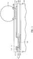
- FIG. 1 is a schematic cross section showing a wafer-level chip-size package (WLCSP) according to an embodiment of the present disclosure.
- WLCSP wafer-level chip-size package
- the WLCSP comprises a semiconductor structure 100, a bonding pad 102, a passivation layer 104, a first planarization layer 106, a second planarization layer 112, a conductive redistribution layer 110, an under-bump-metallurgy (UBM) layer 116, and a conductive bump 118.
- UBM under-bump-metallurgy
- the bonding pad 102 is formed over a portion of the semiconductor structure 100 and may be electrically connected with one of the interconnect structure (not shown) of a circuit formed in the semiconductor structure 100.
- the passivation layer 104 and the first planarization layer 106 are sequentially formed over the semiconductor structure 100, and the passivation layer 104 and the first planarization layer 106 partially respectively cover portions of the bonding pad 102.
- An opening 108 is formed in the first planarization layer 106 to expose a portion of the bonding pad 102, and the conductive redistribution layer 110 is conformably formed over portions of the first planarization layer 106 and in the opening to cover the portion of the bonding pad 102 exposed by the opening 108.
- the bonding pad 102 may comprise conductive materials such as aluminum, and the passivation layer 104 may comprise dielectric materials such as silicon oxide, silicon nitride, or a combination thereof.
- the first planarization layer 106 and the second planarization layer 112 may comprise dielectric materials such as silicon nitride, silicon oxide, or polymer.
- the polymer suitable for the first planarization layer 106 and the second planarization layer 112 can be, for example, polyimide, polybenzoxazole or benzocyclobutene.
- the conductive redistribution layer 110 may comprise conductive materials such as copper, nickel, or aluminum.
- the conductive redistribution layer 110 is conformably formed over portions of the first planarization layer 106 and the portion of the bonding pad 102 exposed by the opening 108 and has a step portion A of a step-like configuration near the opening 108 and a planar portion B of a flat configuration extending from the opening 114 and over the first planarization layer 106.
- the opening 114 formed in the second planarization layer 112 exposes a portion of the planar portion B of the conductive redistribution layer 110, so that the UBM layer 116 can be conformably disposed over portions of the second planarization layer 112 and the planar portion B of the conductive redistribution layer 110 exposed by the opening 114.
- the step-height of the first planarization layer 106 near the opening 108 is too great to make the opening 108 smaller.
- the portion of the conductive redistribution layer 110 near the opening 108 is formed with a step-like configuration, and the UBM layer 116 and the solder bump 118 formed over the UBM layer only can be formed over the planar portion B of the conductive redistribution layer 110 extending from the opening 108 and over the first passivation layer 106.
- the bonding pad 102 exposed by the opening formed in the passivation layer 104 will be provided with a configuration as a large-sized conductive pad with only one electrical potential during operation of the WLCSP shown in FIG. 1 . Therefore, the footprint of the WLCSP shown in FIG. 1 is quite large and there is no chance for forming another conductive component adjacent to the bonding pad 102 for providing another electrical potential during operation of the WLCSP shown in FIG. 1 , which is undesirable because of the trend towards further reduction in the size of the integrated circuits in the WLCSP.
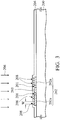
- a semiconductor structure 200 having a bonding pad 202 and a conductive component 203 formed over various portions of the semiconductor structure 200 is provided.
- the bonding pad 202 comprises a plurality of conductive segments 202a separately formed over the semiconductor structure 200 and the conductive component 203 is adjacent to the bonding pad 202.
- the bonding pad 202 comprises two conductive segments 202a formed over various portions of the semiconductor structure 200, and the conductive component 203 is formed over the semiconductor substrate 200 at a place between the conductive segments 202a of the bonding pad 202.
- the conductive component 203 is isolated from the two conductive segments 202a of the bonding pad 202 by a trench 201 formed between the conductive component 203 and one of the conductive segments 202a of the bonding pad 202.
- the conductive component 203 and the conductive segments 202a of the bonding pad 202 comprises the same conductive materials such as Al, Cu or W, and can be simultaneously formed.
- a passivation layer 204 is next conformably formed over the semiconductor structure 200, the bonding pad 202, and the conductive component 203 by, for example, a chemical vapor deposition (CVD) process (not shown).
- the passivation layer 204 is conformably formed over the semiconductor structure 200, the bonding pad 202, and the conductive component 203, and fills each of the trenches 201.
- the passivation layer 204 has a non-planar top surface over the semiconductor structure 200.
- the portion of the passivation layer 204 formed over the semiconductor structure 200 has a thickness T of about 0.8 ⁇ m to about 4 ⁇ m.
- the semiconductor structure 200 is the same as the semiconductor structure 100 shown in FIG. 1 , and materials for forming the passivation layer 204, and the bonding pad 202 and the conductive component 203 are similar with those used for forming the passivation layer 104 and the bonding pad 102 shown in FIG. 1 .
- a patterning process 206 is next performed on the passivation layer 204 shown in FIG. 2 to form a plurality of openings 208 only in portions of the passivation layer 204 over the conductive segments 202a of the bonding pad 202.
- a first planarization layer 210 is formed over the top surface of the structure shown in FIG. 3 , and a patterning process 212 is next performed on the first planarization layer 210 to form an opening 214 in a portion of the first planarization layer 210, thereby exposing the portion of the passivation layer 204 formed over the conductive components 203 and the conductive segments 202a of the bonding pad 202, the openings 208, and the portions of the conductive segments 202a of the bonding pad 202 exposed by the opening 208.
- the first planarization layer 210 can be formed by chemical vapor deposition (CVD) or spin coating, for example, and may be patterned by the patterning process 212 comprising photolithography and etching steps (not shown) incorporating suitable patterned masks (not shown) as an etching mask. Materials for forming the first planarization layer 210 can be the same as those of the first planarization layer 106 shown in FIG. 1 , and the first planarization layer 210 may have a thickness of about ⁇ m to about ⁇ m.
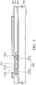
- a patterned conductive redistribution layer 216 is next formed over portions of the passivation layer 204 exposed by the opening 214 and portions of the first planarization layer 210.
- the portion of the patterned conductive redistribution layer 216 formed in the opening 214 fills the openings 208 exposing the portions of the conductive segments 202a of the bonding pad 202 and covers the portion of the passivation layer 204 formed over the conductive components 203, comprising a plurality of first portions 216a filling the openings 208 formed in the passivation layer 204, and a second portion 216b formed above the flat top surface of the passivation layer 204 and the openings 208.
- the patterned conductive redistribution layer 216 is also provided with a conformal top surface, as shown in FIG. 5 .
- the patterned conductive redistribution layer 216 can be formed by first forming a conductive redistribution layer over the passivation layer 204 and in the openings 208, and then the conductive redistribution layer is patterned by a patterning process (not shown) comprising photolithography and etching steps (not shown) incorporating suitable patterned masks (not shown) as an etching mask.
- Conductive materials for forming the patterned conductive redistribution layer 216 can be the same as those of the conductive redistribution layer 110 shown in FIG. 1 , with a thickness of about 4 ⁇ m to about 9 ⁇ m above the passivation layer 204.
- a second planarization layer 218 is formed over the top surface of the structure shown in FIG. 5 , and a patterning process 220 is next performed on the second planarization layer 218 to form an opening 222 in a portion of the second planarization layer 218, thereby exposing a portion of the patterned redistribution layer 216.
- the second planarization layer 208 can be formed by chemical vapor deposition (CVD) or spin coating, for example, and may be patterned by the patterning process 220 comprising photolithography and etching steps (not shown) incorporating suitable patterned masks (not shown) as an etching mask.
- Materials for forming the second planarization layer 218 can be the same as those of the first planarization layer 112 shown in FIG. 1 , and the second planarization layer 218 may have a thickness of about 7.5 ⁇ m to about 10 ⁇ m, which is greater than the thickness of the patterned conductive redistribution layer 216.
- an under-bump-metallurgy (UBM) layer 224 is next formed over the portion of the patterned conductive redistribution layer 216 exposed by the opening 222.
- the UBM layer 218 can be formed by forming a layer of conductive material over the structure shown in FIG. 6 by, for example, chemical vapor deposition (CVD) or electrical plating, and is then patterned by a patterning process (not shown) comprising photolithography and etching steps (not shown) incorporating suitable patterned masks (not shown) as an etching mask.
- Materials for forming the UBM layer 224 can be the same as that of the UBM layer 116 shown in FIG. 1 , and the UBM layer 224 may have a thickness of about ⁇ m to about ⁇ m.
- a conductive bump 226 is next formed over the UBM layer 224 by conventional solder bump formation processes.
- the UBM layer 224 and the conductive bump 226 can be sequentially and firmly formed over the patterned conductive redistribution layer 216. Therefore, a wafer-level chip-size package (WLCSP) having an additional conductive component adjacent to the bonding pad is substantially formed.
- WLCSP wafer-level chip-size package
- the wafer-level chip-size package is provided with an additional conductive component 203 which is electrically isolated from the bonding pad 202 and the patterned redistribution layer 216, such that the conductive component 203 may be designed to function as a signal line, a power line or a ground line that operates in an electrical potential that is different from that of the bonding pad 202 during operation of the WLCSP shown in FIG. 8 .
- the size of the conductive segments 202a of the bonding pad 202 can be reduced to a smaller size than the conventional pad 102 shown in FIG. 1 . Therefore, the WLCSP shown in FIG. 8 allows for a multifunctional design in a more compact structure, which is desired as the trend continues towards further reduction in the size of integrated circuits in WLCSP.
- FIG. 9 is a schematic top view showing a region comprising the bonding pad 202 and the conductive component 203 of the WLCSP shown in FIG. 8 .
- the conductive component 203 is disposed between the conductive segments 202a of the bonding pad 202.
- the conductive component 203 is formed with a strip-like configuration extending both upward and downward, and the conductive segments 202a of the bonding pad 202 are formed with a pad-like configuration having a maximum size (e.g. length) that is less than that of the conductive component 203.
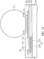
- FIG. 10 is a schematic cross section showing another exemplary wafer-level chip-size package (WLCSP) of the present disclosure.
- WLCSP wafer-level chip-size package
- the location of the conductive component 203 is switched with one of the conductive segments 202a of the bonding pad 202, such that the conductive component 203 is formed at the left side of the conductive segments 202a of the bonding pad 202. As shown in FIG. 10 , the conductive component 203 is adjacent to only one of the conductive segments 202a of the bonding pad 202.
- FIG. 11 is a schematic top view showing a region comprising the bonding pad 202 and the conductive component 203 of the WLCSP shown in FIG. 10 .
- the conductive component 203 is disposed at the left side of the conductive segments 202a of the bonding pad 202.
- the conductive component 203 is formed with a strip-like configuration extending both upward and downward, and the conductive segments 202a of the bonding pad 202 are formed with a pad-like configuration having a maximum dimension (e.g. length) less than that of the conductive component 203.
- FIG. 12 is a schematic cross section showing yet another exemplary wafer-level chip-size package (WLCSP) of the present disclosure.
- WLCSP wafer-level chip-size package
- the location of the conductive component 203 is switched with one of the conductive segments 202a of the bonding pad 202, such that the conductive component 203 is formed at the right side of the conductive segments 202a of the bonding pad 202. As shown in FIG. 12 , the conductive component 203 is adjacent to only one of the conductive segments 202a of the bonding pad 202.
- FIG. 13 is a schematic top view showing a region comprising the bonding pad 202 and the conductive component 203 of the WLCSP shown in FIG. 12 .
- the conductive component 203 is disposed at the right side of the conductive segments 202a of the bonding pad 202.
- the conductive component 203 is formed with a strip-like configuration extending both upward and downward, and the conductive segments 202a of the bonding pad 202 are formed with a pad-like configuration having a maximum dimension (e.g. length) that is less than that of the conductive component 203.
Landscapes
- Internal Circuitry In Semiconductor Integrated Circuit Devices (AREA)
- Engineering & Computer Science (AREA)
- Manufacturing & Machinery (AREA)
Abstract
Description
- This application claims the benefit of
U.S. Provisional Application No. 62/306,657 filed March 11, 2016 - The present invention relates to integrated circuits (ICs), and in particular to a wafer-level chip-size package (WLCSP) with a redistribution layer and a method for forming the same.
- The desire to make electronic products small, lightweight, and high-performing has developed into a desire to make electronic parts small, lightweight, and high-performing. This desire has caused developments to proceed in various packaging technologies, along with developments in the technologies related to designing and manufacturing semiconductors. Representative examples of packaging technologies include the ball grid array (BGA), the flip-chip, and the chip size package (CSP) based on area array and surface-mount packaging.
- Among the above, the CSP is a packaging technology that enables a small package to be the same size as the real chip to be developed. In particular, in a wafer-level chip-size package (WLCSP), the packaging is performed in a wafer level so that the packaging costs per chip can be remarkably reduced. Typically, the WLCSP includes a redistribution layer (RDL) wiring traces, an under bump metallurgy (UBM) layer forming a bump, and a passivation layer protecting a circuit.
- An exemplary wafer-level chip-size package comprises a semiconductor structure, a bonding pad, a conductive component, a passivation layer, a conductive redistribution layer, an under-bump-metallurgy (UBM) layer, and a conductive bump. The bonding pad is formed over the semiconductor structure and comprises a plurality of conductive segments. The conductive component is formed over the semiconductor structure, and is adjacent to the bonding pad. The passivation layer is formed over the semiconductor structure, the first bonding pad and the conductive component, and exposes portions of the conductive segments of the first bonding pad. The conductive redistribution layer is formed over the passivation layer and the portions of the conductive segments of the first bonding pad exposed by the passivation layer. The planarization layer is formed over the passivation layer and the conductive redistribution layer, and exposes a portion of the conductive redistribution layer. The UBM layer is formed over the planarization layer and the portion of the conductive redistribution layer exposed by the planarization layer. The conductive bump is formed over the UBM layer.
- An exemplary method for forming a wafer-level chip-size package comprises providing a semiconductor structure having a bonding pad and a conductive component formed over the semiconductor structure, wherein the bonding pad comprises a plurality of conductive segments, and the conductive component is adjacent to the bonding pad. The method further comprises forming a passivation layer over the semiconductor structure, the bonding pad, and the conductive component, wherein the passivation layer exposes a plurality of portions of the conductive segments of the bonding pad. The method further comprises forming a conductive redistribution layer over the passivation layer and the portions of the conductive segments of the bonding pad exposed by the passivation layer. The method further comprises forming a planarization layer over the passivation layer and the conductive redistribution layer, and exposing a portion of the conductive redistribution layer. The method further comprises forming an under-bump-metallurgy (UBM) layer over the portion of the conductive redistribution layer exposed by the planarization layer. The method further comprises forming a conductive bump formed over the UBM layer.
- A detailed description is given in the following embodiments with reference to the accompanying drawings.
- The invention can be more fully understood by reading the subsequent detailed description and examples with references made to the accompanying drawings, wherein:
-
FIG. 1 is a schematic cross section showing a wafer-level chip-size package (WLCSP) according to an embodiment of the present disclosure; -
FIGs. 2-8 are a schematic cross sections showing a method for forming a wafer-level chip-size package (WLCSP) according to an embodiment of the present disclosure; -
FIG. 9 is a schematic top view showing a region of the wafer-level chip-size package (WLCSP) inFIG. 8 ; -
FIG. 10 is a schematic cross section showing a wafer-level chip-size package (WLCSP) according to another embodiment of the present disclosure; -
FIG. 11 is a schematic top view showing a region of the wafer-level chip-size package (WLCSP) inFIG. 10 ; -
FIG. 12 is a schematic cross section showing a wafer-level chip-size package (WLCSP) according to yet another embodiment of the present disclosure; and -
FIG. 13 is a schematic top view showing a region of the wafer-level chip-size package (WLCSP) inFIG. 12 . - The following description is of the best-contemplated mode of carrying out the invention. This description is made for the purpose of illustrating the general principles of the invention and should not be taken in a limiting sense. The scope of the invention is best determined by reference to the appended claims.
-
FIG. 1 is a schematic cross section showing a wafer-level chip-size package (WLCSP) according to an embodiment of the present disclosure. - As shown in
FIG. 1 , the WLCSP comprises asemiconductor structure 100, abonding pad 102, apassivation layer 104, afirst planarization layer 106, asecond planarization layer 112, aconductive redistribution layer 110, an under-bump-metallurgy (UBM)layer 116, and aconductive bump 118. - Herein, the
semiconductor structure 100 is illustrated as a structure having a flat top surface for the purpose of simplifying the figure. It should be noted that thesemiconductor structure 100 can be a wafer-level semiconductor substrate having a plurality of semiconductor devices and interconnect structures (both not shown) formed thereon. The semiconductor devices formed over thesemiconductor substrate 100 can be, for example, active devices such as transistors or diodes and/or passive devices such as capacitors, resistors and conductors. The interconnect structures in thesemiconductor structure 100 may comprise a multi-layer metallization structure isolated and supported by a plurality of interlayer dielectric layers. In this embodiment, only a portion of thesemiconductor structure 100 is illustrated as the WLCSP. - Referring to
FIG. 1 , thebonding pad 102 is formed over a portion of thesemiconductor structure 100 and may be electrically connected with one of the interconnect structure (not shown) of a circuit formed in thesemiconductor structure 100. Thepassivation layer 104 and thefirst planarization layer 106 are sequentially formed over thesemiconductor structure 100, and thepassivation layer 104 and thefirst planarization layer 106 partially respectively cover portions of thebonding pad 102. Anopening 108 is formed in thefirst planarization layer 106 to expose a portion of thebonding pad 102, and theconductive redistribution layer 110 is conformably formed over portions of thefirst planarization layer 106 and in the opening to cover the portion of thebonding pad 102 exposed by theopening 108. Thesecond planarization layer 112 is formed over thefirst planarization layer 106 and theconductive redistribution layer 110, and anopening 114 is formed in thesecond planarization layer 112 to expose a portion of theconductive redistribution layer 110. TheUBM layer 116 is formed over a portion of thesecond planarization layer 112 and the portion of theconductive redistribution layer 110 exposed by thesecond planarization layer 112, and theconductive bump 118 is formed over theUBM layer 116. - In this embodiment, the
bonding pad 102 may comprise conductive materials such as aluminum, and thepassivation layer 104 may comprise dielectric materials such as silicon oxide, silicon nitride, or a combination thereof. Thefirst planarization layer 106 and thesecond planarization layer 112 may comprise dielectric materials such as silicon nitride, silicon oxide, or polymer. In one embodiment, the polymer suitable for thefirst planarization layer 106 and thesecond planarization layer 112 can be, for example, polyimide, polybenzoxazole or benzocyclobutene. Theconductive redistribution layer 110 may comprise conductive materials such as copper, nickel, or aluminum. TheUBM layer 116 may comprise conductive materials such as metals or metal alloys such as Ni layers, Ag layers, A1 layers, Cu layers or alloys thereof, or materials of doped polysilicon, monocrystalline silicon or conductive glasses. Additionally, refractory metal materials such as titanium, molybdenum, chromium or titanium tungsten layers can be used to individually form the UBM layers or be combined with other metal layers. Typically, thefirst planarization layer 106 is provided with a thickness C of about 5 µm to about 7.5 µm, and the step-height of thefirst planarization layer 106 over thebonding pad 102 is too great, and as a result theopening 108 formed in thefirst planarization layer 106 is smaller than the opening formed in thepassivation layer 104, having a size of, for example, about µm to about µm. Therefore, theconductive redistribution layer 110 is conformably formed over portions of thefirst planarization layer 106 and the portion of thebonding pad 102 exposed by theopening 108 and has a step portion A of a step-like configuration near theopening 108 and a planar portion B of a flat configuration extending from the opening 114 and over thefirst planarization layer 106. In addition, theopening 114 formed in thesecond planarization layer 112 exposes a portion of the planar portion B of theconductive redistribution layer 110, so that theUBM layer 116 can be conformably disposed over portions of thesecond planarization layer 112 and the planar portion B of theconductive redistribution layer 110 exposed by theopening 114. - In the WLCSP shown in
FIG. 1 , since thefirst planarization layer 106, having a thickness C of about 5 µm to about 7.5 µm is provided, the step-height of thefirst planarization layer 106 near theopening 108 is too great to make theopening 108 smaller. Thus, the portion of theconductive redistribution layer 110 near theopening 108 is formed with a step-like configuration, and theUBM layer 116 and thesolder bump 118 formed over the UBM layer only can be formed over the planar portion B of theconductive redistribution layer 110 extending from theopening 108 and over thefirst passivation layer 106. Moreover, since the opening formed in thepassivation layer 104 needs to be formed in a size that is greater than the size of theopening 108 formed in thefirst planarization layer 106, thebonding pad 102 exposed by the opening formed in thepassivation layer 104 will be provided with a configuration as a large-sized conductive pad with only one electrical potential during operation of the WLCSP shown inFIG. 1 . Therefore, the footprint of the WLCSP shown inFIG. 1 is quite large and there is no chance for forming another conductive component adjacent to thebonding pad 102 for providing another electrical potential during operation of the WLCSP shown inFIG. 1 , which is undesirable because of the trend towards further reduction in the size of the integrated circuits in the WLCSP. - Therefore,
FIGs. 2-8 are schematic cross sections showing a method for forming a wafer-level chip-size package (WLCSP) having an additional conductive component adjacent to the bonding pad for providing another electrical potential that is different from that of the bonding pad, according to another embodiment of the present disclosure. - Referring to
FIG. 2 , asemiconductor structure 200 having abonding pad 202 and aconductive component 203 formed over various portions of thesemiconductor structure 200 is provided. Thebonding pad 202 comprises a plurality ofconductive segments 202a separately formed over thesemiconductor structure 200 and theconductive component 203 is adjacent to thebonding pad 202. In one embodiment, as shown inFIG. 2 , thebonding pad 202 comprises twoconductive segments 202a formed over various portions of thesemiconductor structure 200, and theconductive component 203 is formed over thesemiconductor substrate 200 at a place between theconductive segments 202a of thebonding pad 202. Theconductive component 203 is isolated from the twoconductive segments 202a of thebonding pad 202 by atrench 201 formed between theconductive component 203 and one of theconductive segments 202a of thebonding pad 202. Theconductive component 203 and theconductive segments 202a of thebonding pad 202 comprises the same conductive materials such as Al, Cu or W, and can be simultaneously formed. - Still referring to
FIG. 2 , apassivation layer 204 is next conformably formed over thesemiconductor structure 200, thebonding pad 202, and theconductive component 203 by, for example, a chemical vapor deposition (CVD) process (not shown). Thepassivation layer 204 is conformably formed over thesemiconductor structure 200, thebonding pad 202, and theconductive component 203, and fills each of thetrenches 201. As shown inFIG. 2 , thepassivation layer 204 has a non-planar top surface over thesemiconductor structure 200. In one embodiment, the portion of thepassivation layer 204 formed over thesemiconductor structure 200 has a thickness T of about 0.8 µm to about 4 µm. - In one embodiment, the
semiconductor structure 200 is the same as thesemiconductor structure 100 shown inFIG. 1 , and materials for forming thepassivation layer 204, and thebonding pad 202 and theconductive component 203 are similar with those used for forming thepassivation layer 104 and thebonding pad 102 shown inFIG. 1 . - Referring to
FIG. 3 , apatterning process 206 is next performed on thepassivation layer 204 shown inFIG. 2 to form a plurality ofopenings 208 only in portions of thepassivation layer 204 over theconductive segments 202a of thebonding pad 202. - As shown in
FIG. 3 , theopenings 208 respectively expose a portion of theconductive segments 202a of thebonding pad 202. However, there is noopening 208 formed in the portion of thepassivation layer 204 over theconductive component 203, and so theconductive component 203 is still covered by thepassivation layer 204 and will not be exposed by theopenings 208. Each of theopenings 208 has a dimension W, for example a width, of about 2 µm to about 90 µm, and theopenings 208 may have a circular, stripe-like, or polygonal shape from a top view (not shown). In one embodiment, thepatterning process 206 may comprise photolithography and etching steps (not shown) with suitable patterned masks (not shown) used as an etching mask (not shown). - Referring to
FIG. 4 , afirst planarization layer 210 is formed over the top surface of the structure shown inFIG. 3 , and apatterning process 212 is next performed on thefirst planarization layer 210 to form anopening 214 in a portion of thefirst planarization layer 210, thereby exposing the portion of thepassivation layer 204 formed over theconductive components 203 and theconductive segments 202a of thebonding pad 202, theopenings 208, and the portions of theconductive segments 202a of thebonding pad 202 exposed by theopening 208. Thefirst planarization layer 210 can be formed by chemical vapor deposition (CVD) or spin coating, for example, and may be patterned by thepatterning process 212 comprising photolithography and etching steps (not shown) incorporating suitable patterned masks (not shown) as an etching mask. Materials for forming thefirst planarization layer 210 can be the same as those of thefirst planarization layer 106 shown inFIG. 1 , and thefirst planarization layer 210 may have a thickness of about µm to about µm. - Referring to
FIG. 5 , a patternedconductive redistribution layer 216 is next formed over portions of thepassivation layer 204 exposed by theopening 214 and portions of thefirst planarization layer 210. As shown inFIG. 5 , the portion of the patternedconductive redistribution layer 216 formed in theopening 214 fills theopenings 208 exposing the portions of theconductive segments 202a of thebonding pad 202 and covers the portion of thepassivation layer 204 formed over theconductive components 203, comprising a plurality offirst portions 216a filling theopenings 208 formed in thepassivation layer 204, and asecond portion 216b formed above the flat top surface of thepassivation layer 204 and theopenings 208. Therefore, the patternedconductive redistribution layer 216 is also provided with a conformal top surface, as shown inFIG. 5 . The patternedconductive redistribution layer 216 can be formed by first forming a conductive redistribution layer over thepassivation layer 204 and in theopenings 208, and then the conductive redistribution layer is patterned by a patterning process (not shown) comprising photolithography and etching steps (not shown) incorporating suitable patterned masks (not shown) as an etching mask. Conductive materials for forming the patternedconductive redistribution layer 216 can be the same as those of theconductive redistribution layer 110 shown inFIG. 1 , with a thickness of about 4 µm to about 9 µm above thepassivation layer 204. - Referring to
FIG. 6 , asecond planarization layer 218 is formed over the top surface of the structure shown inFIG. 5 , and apatterning process 220 is next performed on thesecond planarization layer 218 to form anopening 222 in a portion of thesecond planarization layer 218, thereby exposing a portion of the patternedredistribution layer 216. Thesecond planarization layer 208 can be formed by chemical vapor deposition (CVD) or spin coating, for example, and may be patterned by thepatterning process 220 comprising photolithography and etching steps (not shown) incorporating suitable patterned masks (not shown) as an etching mask. Materials for forming thesecond planarization layer 218 can be the same as those of thefirst planarization layer 112 shown inFIG. 1 , and thesecond planarization layer 218 may have a thickness of about 7.5 µm to about 10 µm, which is greater than the thickness of the patternedconductive redistribution layer 216. - Referring to
FIG. 7 , an under-bump-metallurgy (UBM)layer 224 is next formed over the portion of the patternedconductive redistribution layer 216 exposed by theopening 222. TheUBM layer 218 can be formed by forming a layer of conductive material over the structure shown inFIG. 6 by, for example, chemical vapor deposition (CVD) or electrical plating, and is then patterned by a patterning process (not shown) comprising photolithography and etching steps (not shown) incorporating suitable patterned masks (not shown) as an etching mask. Materials for forming theUBM layer 224 can be the same as that of theUBM layer 116 shown inFIG. 1 , and theUBM layer 224 may have a thickness of about µm to about µm. - Referring to
FIG. 8 , aconductive bump 226 is next formed over theUBM layer 224 by conventional solder bump formation processes. TheUBM layer 224 and theconductive bump 226 can be sequentially and firmly formed over the patternedconductive redistribution layer 216. Therefore, a wafer-level chip-size package (WLCSP) having an additional conductive component adjacent to the bonding pad is substantially formed. - As shown in
FIG. 8 , since the wafer-level chip-size package (WLCSP) is provided with an additionalconductive component 203 which is electrically isolated from thebonding pad 202 and thepatterned redistribution layer 216, such that theconductive component 203 may be designed to function as a signal line, a power line or a ground line that operates in an electrical potential that is different from that of thebonding pad 202 during operation of the WLCSP shown inFIG. 8 . In addition, due to formation of theconductive component 203, the size of theconductive segments 202a of thebonding pad 202 can be reduced to a smaller size than theconventional pad 102 shown inFIG. 1 . Therefore, the WLCSP shown inFIG. 8 allows for a multifunctional design in a more compact structure, which is desired as the trend continues towards further reduction in the size of integrated circuits in WLCSP. -
FIG. 9 is a schematic top view showing a region comprising thebonding pad 202 and theconductive component 203 of the WLCSP shown inFIG. 8 . InFIG. 9 , only thebonding pad 202 and theconductive component 203 are illustrated but other components are omitted for the ease of showing an arrangement of thebonding pad 202 and theconductive component 203. As shown inFIG. 9 , theconductive component 203 is disposed between theconductive segments 202a of thebonding pad 202. Theconductive component 203 is formed with a strip-like configuration extending both upward and downward, and theconductive segments 202a of thebonding pad 202 are formed with a pad-like configuration having a maximum size (e.g. length) that is less than that of theconductive component 203. - In addition to the exemplary embodiment shown in
FIG. 8 ,FIG. 10 is a schematic cross section showing another exemplary wafer-level chip-size package (WLCSP) of the present disclosure. At this time, the WLCSP shown inFIG. 10 is modified from the WLCSP shown inFIG. 8 , and similar components inFIG. 10 are represented with the same reference numbers shown inFIG. 8 , and only differences between the WLCSPs shown inFIGs. 8 and10 are discussed below. - Referring to
FIG. 10 , the location of theconductive component 203 is switched with one of theconductive segments 202a of thebonding pad 202, such that theconductive component 203 is formed at the left side of theconductive segments 202a of thebonding pad 202. As shown inFIG. 10 , theconductive component 203 is adjacent to only one of theconductive segments 202a of thebonding pad 202. -
FIG. 11 is a schematic top view showing a region comprising thebonding pad 202 and theconductive component 203 of the WLCSP shown inFIG. 10 . Similarly, inFIG. 11 , only thebonding pad 202 and theconductive component 203 are illustrated while other components are omitted for the ease of showing an arrangement of thebonding pad 202 and theconductive component 203. As shown inFIG. 11 , theconductive component 203 is disposed at the left side of theconductive segments 202a of thebonding pad 202. Theconductive component 203 is formed with a strip-like configuration extending both upward and downward, and theconductive segments 202a of thebonding pad 202 are formed with a pad-like configuration having a maximum dimension (e.g. length) less than that of theconductive component 203. - Moreover, in addition to the exemplary embodiments shown in
FIG. 8 ,FIG. 12 is a schematic cross section showing yet another exemplary wafer-level chip-size package (WLCSP) of the present disclosure. At this time, the WLCSP shown inFIG. 12 is modified from the WLCSP shown inFIG. 8 , and similar components inFIG. 12 are represented with the same reference numbers shown inFIG. 8 , and only differences between the WLCSPs shown inFIGs. 8 and12 are discussed below. - Referring to
FIG. 12 , the location of theconductive component 203 is switched with one of theconductive segments 202a of thebonding pad 202, such that theconductive component 203 is formed at the right side of theconductive segments 202a of thebonding pad 202. As shown inFIG. 12 , theconductive component 203 is adjacent to only one of theconductive segments 202a of thebonding pad 202. -
FIG. 13 is a schematic top view showing a region comprising thebonding pad 202 and theconductive component 203 of the WLCSP shown inFIG. 12 . Similarly, inFIG. 13 , only thebonding pad 202 and theconductive component 203 are illustrated but other components are omitted for the ease of showing an arrangement of thebonding pad 202 and theconductive component 203. As shown inFIG. 13 , theconductive component 203 is disposed at the right side of theconductive segments 202a of thebonding pad 202. Theconductive component 203 is formed with a strip-like configuration extending both upward and downward, and theconductive segments 202a of thebonding pad 202 are formed with a pad-like configuration having a maximum dimension (e.g. length) that is less than that of theconductive component 203. - Similarly with the embodiment shown in
FIGs. 8-9 , since the wafer-level chip-size package (WLCSP) of the embodiments shown inFIGs. 10-12 are also provided with an additionalconductive component 203 which is electrically isolated from thebonding pad 202 and thepatterned redistribution layer 216, such that theconductive component 203 may be designed to function as a signal line, a power line or a ground line that operates in an electrical potential that is different from that of thebonding pad 202 during operation of the WLCSP shown inFIG. 8 . In addition, due to the formation of theconductive component 203, the size of theconductive segments 202a of thebonding pad 202 can be reduced to a smaller size than theconventional pad 102 shown inFIG. 1 . Therefore, the WLCSP shown inFIGs. 10-13 allows for a multifunctional design in a more compact structure, which is desired as the trend towards further reduction in the size of integrated circuits in WLCSP continues. - While the invention has been described by way of example and in terms of the preferred embodiments, it is to be understood that the invention is not limited to the disclosed embodiments. On the contrary, it is intended to cover various modifications and similar arrangements (as would be apparent to those skilled in the art). Therefore, the scope of the appended claims should be accorded the broadest interpretation so as to encompass all such modifications and similar arrangements.
Claims (15)
- A wafer-level chip-size package, comprising:a semiconductor structure;a bonding pad formed over the semiconductor structure, comprising a plurality of conductive segments;a conductive component formed over the semiconductor structure, being adjacent to the bonding pad;a passivation layer formed over the semiconductor structure, the first bonding pad and the conductive component, wherein the passivation layer exposes portions of the conductive segments of the first bonding pad;a conductive redistribution layer formed over the passivation layer and the portion of the conductive segments of the first bonding pad exposed by the passivation layer;a planarization layer formed over the passivation layer and the conductive redistribution layer, exposing a portion of the conductive redistribution layer;an under-bump-metallurgy (UBM) layer formed over the planarization layer and the portion of the conductive redistribution layer exposed by the planarization layer; anda conductive bump formed over the UBM layer.
- The wafer-level chip-size package as claimed in claim 1, wherein the conductive component is disposed between two of the conductive segments of the bonding pad.
- The wafer-level chip-size package as claimed in claim 1, wherein the conductive component is disposed at a left side of the conductive segments of the bonding pad.
- The wafer-level chip-size package as claimed in claim 1, wherein the conductive component is disposed at a right side of the conductive segments of the bonding pad.
- The wafer-level chip-size package as claimed in one of the preceding claims, wherein the passivation layer comprises dielectric materials.
- The wafer-level chip-size package as claimed in one of the preceding claims , wherein the planarization layer comprises polyimide, polybenzoxazole or benzocyclobutene.
- The wafer-level chip-size package as claimed in one of the preceding claims , wherein the UBM layer is formed over the portion of the conductive redistribution layer at a place that is not over the portions of the conductive segments of the bonding pad exposed by the passivation layer.
- The wafer-level chip-size package as claimed in one of the preceding claims , wherein the portions of the conductive segments of the bonding pad exposed by the passivation layer have a size of about 2 µm to about 90 µm.
- The wafer-level chip-size package as claimed in one of the preceding claims , wherein the portions of the conductive segments of the bonding pad exposed by the passivation layer respectively have a circular, stripe-like, or polygonal shape.
- The wafer-level chip-size package as claimed in one of the preceding claims , wherein the conductive component has a strip-like configuration from a top view.
- A method for forming a wafer-level chip-size package, comprising:providing a semiconductor structure having a bonding pad and a conductive component formed over the semiconductor structure, wherein the bonding pad comprises a plurality of conductive segments, and the conductive component is adjacent to the bonding pad;forming a passivation layer over the semiconductor structure, the bonding pad, and the conductive component, wherein the passivation layer exposes a plurality of portions of the conductive segments of the bonding pad;forming a conductive redistribution layer over the passivation layer and the portions of the conductive segments of the bonding pad exposed by the passivation layer;forming a planarization layer over the passivation layer and the conductive redistribution layer, exposing a portion of the conductive redistribution layer;forming an under-bump-metallurgy (UBM) layer over the portion of the conductive redistribution layer exposed by the planarization layer; andforming a conductive bump formed over the UBM layer.
- The method as claimed in claim 11, wherein formation of the passivation layer over the semiconductor structure, the bonding pad, and the conductive component comprises:conformably forming the passivation layer over the semiconductor structure, the bonding pad, and the conductive component; andforming a plurality of first openings in the passivation layer and exposing the plurality of portions of the conductive segments of the bonding pad.
- The method as claimed in claim 11 or 12, wherein formation of the planarization layer over the passivation layer and the conductive redistribution layer to expose a portion of the conductive redistribution layer comprises:forming the planarization layer formed over the passivation layer and the conductive redistribution layer; andforming an opening in a portion of the planarization layer and exposing the portion of the conductive redistribution layer.
- The method as claimed in claim 11, wherein the portions of the conductive segments of the bonding pad exposed by the passivation layer respectively have a circular, stripe-like, or polygonal shape and/or
wherein the portions of the conductive segments of the bonding pad exposed by the passivation layer respectively have a dimension of about 2 µm to about 90 µm. - The method as claimed in one of claims 11 to 14, wherein the portions of the conductive segments of the bonding pad exposed by the passivation layer respectively have a circular, stripe-like, or polygonal shape, and/or
wherein the conductive component has a strip-like configuration from a top view.
Applications Claiming Priority (2)
| Application Number | Priority Date | Filing Date | Title |
|---|---|---|---|
| US201662306657P | 2016-03-11 | 2016-03-11 | |
| US15/286,844 US10998267B2 (en) | 2016-03-11 | 2016-10-06 | Wafer-level chip-size package with redistribution layer |
Publications (2)
| Publication Number | Publication Date |
|---|---|
| EP3217427A1 true EP3217427A1 (en) | 2017-09-13 |
| EP3217427B1 EP3217427B1 (en) | 2021-11-10 |
Family
ID=57354208
Family Applications (1)
| Application Number | Title | Priority Date | Filing Date |
|---|---|---|---|
| EP16199543.6A Active EP3217427B1 (en) | 2016-03-11 | 2016-11-18 | Wafer-level chip-size package with redistribution layer |
Country Status (4)
| Country | Link |
|---|---|
| US (1) | US10998267B2 (en) |
| EP (1) | EP3217427B1 (en) |
| CN (1) | CN107180812A (en) |
| TW (1) | TWI601254B (en) |
Cited By (1)
| Publication number | Priority date | Publication date | Assignee | Title |
|---|---|---|---|---|
| CN113053845A (en) * | 2019-12-27 | 2021-06-29 | 意法半导体有限公司 | WLCSP package with different solder volumes |
Families Citing this family (10)
| Publication number | Priority date | Publication date | Assignee | Title |
|---|---|---|---|---|
| WO2020227896A1 (en) * | 2019-05-13 | 2020-11-19 | Boe Technology Group Co., Ltd. | Array substrate, display apparatus, and method of fabricating array substrate |
| CN110299330A (en) * | 2019-05-29 | 2019-10-01 | 宁波芯健半导体有限公司 | A kind of encapsulating structure and packaging method of wafer stage chip |
| US20210210462A1 (en) * | 2020-01-06 | 2021-07-08 | Texas Instruments Incorporated | Chip scale package with redistribution layer interrupts |
| TWI766280B (en) * | 2020-05-14 | 2022-06-01 | 南茂科技股份有限公司 | Wafer level chip scale package structure and method for manufacturing the same |
| CN113990759B (en) * | 2020-12-21 | 2025-07-22 | 矽磐微电子(重庆)有限公司 | Semiconductor packaging method and semiconductor packaging structure |
| US11935852B2 (en) * | 2021-04-08 | 2024-03-19 | Mediatek Inc. | Semiconductor package and manufacturing method thereof |
| US12107059B2 (en) * | 2021-04-08 | 2024-10-01 | Mediatek Inc. | Semiconductor package and manufacturing method thereof |
| US12107058B2 (en) * | 2021-08-18 | 2024-10-01 | STATS ChipPAC Pte. Ltd. | Split RDL connection between die and UBM |
| US11862576B2 (en) * | 2021-10-28 | 2024-01-02 | Texas Instruments Incorporated | IC having electrically isolated warpage prevention structures |
| KR20230172679A (en) | 2022-06-15 | 2023-12-26 | 삼성전자주식회사 | Semiconductor package including redistribution structure |
Citations (5)
| Publication number | Priority date | Publication date | Assignee | Title |
|---|---|---|---|---|
| US20110063815A1 (en) * | 2009-09-16 | 2011-03-17 | International Business Machines Corporation | Robust FBEOL and UBM Structure of C4 Interconnects |
| US20120228763A1 (en) * | 2011-03-07 | 2012-09-13 | Renesas Electronics Corporation | Semiconductor device and manufacturing method thereof |
| US20130187269A1 (en) * | 2012-01-24 | 2013-07-25 | Taiwan Semiconductor Manufacturing Company, Ltd. | Package assembly and method of forming the same |
| WO2014174825A1 (en) * | 2013-04-24 | 2014-10-30 | パナソニックIpマネジメント株式会社 | Semiconductor device |
| US20150228594A1 (en) * | 2014-02-13 | 2015-08-13 | Qualcomm Incorporated | Via under the interconnect structures for semiconductor devices |
Family Cites Families (8)
| Publication number | Priority date | Publication date | Assignee | Title |
|---|---|---|---|---|
| US6636313B2 (en) * | 2002-01-12 | 2003-10-21 | Taiwan Semiconductor Manufacturing Co. Ltd | Method of measuring photoresist and bump misalignment |
| KR100804392B1 (en) * | 2005-12-02 | 2008-02-15 | 주식회사 네패스 | Semiconductor package and manufacturing method thereof |
| US20080173904A1 (en) | 2007-01-22 | 2008-07-24 | Taiwan Semiconductor Manufacturing Co., Ltd. | CMOS image sensors with a bonding pad and methods of forming the same |
| US8299632B2 (en) * | 2009-10-23 | 2012-10-30 | Ati Technologies Ulc | Routing layer for mitigating stress in a semiconductor die |
| US9184143B2 (en) | 2013-12-05 | 2015-11-10 | Taiwan Semiconductor Manufacturing Company Ltd. | Semiconductor device with bump adjustment and manufacturing method thereof |
| US9263405B2 (en) | 2013-12-05 | 2016-02-16 | Taiwan Semiconductor Manufacturing Company Ltd. | Semiconductor device |
| TW201541590A (en) | 2014-04-28 | 2015-11-01 | Novatek Microelectronics Corp | Integrated circuit |
| CN105047643A (en) * | 2014-04-28 | 2015-11-11 | 联咏科技股份有限公司 | integrated circuit |
-
2016
- 2016-10-06 US US15/286,844 patent/US10998267B2/en active Active
- 2016-11-18 EP EP16199543.6A patent/EP3217427B1/en active Active
- 2016-12-07 TW TW105140372A patent/TWI601254B/en not_active IP Right Cessation
- 2016-12-12 CN CN201611140300.5A patent/CN107180812A/en not_active Withdrawn
Patent Citations (5)
| Publication number | Priority date | Publication date | Assignee | Title |
|---|---|---|---|---|
| US20110063815A1 (en) * | 2009-09-16 | 2011-03-17 | International Business Machines Corporation | Robust FBEOL and UBM Structure of C4 Interconnects |
| US20120228763A1 (en) * | 2011-03-07 | 2012-09-13 | Renesas Electronics Corporation | Semiconductor device and manufacturing method thereof |
| US20130187269A1 (en) * | 2012-01-24 | 2013-07-25 | Taiwan Semiconductor Manufacturing Company, Ltd. | Package assembly and method of forming the same |
| WO2014174825A1 (en) * | 2013-04-24 | 2014-10-30 | パナソニックIpマネジメント株式会社 | Semiconductor device |
| US20150228594A1 (en) * | 2014-02-13 | 2015-08-13 | Qualcomm Incorporated | Via under the interconnect structures for semiconductor devices |
Cited By (1)
| Publication number | Priority date | Publication date | Assignee | Title |
|---|---|---|---|---|
| CN113053845A (en) * | 2019-12-27 | 2021-06-29 | 意法半导体有限公司 | WLCSP package with different solder volumes |
Also Published As
| Publication number | Publication date |
|---|---|
| CN107180812A (en) | 2017-09-19 |
| EP3217427B1 (en) | 2021-11-10 |
| TWI601254B (en) | 2017-10-01 |
| US20170263523A1 (en) | 2017-09-14 |
| US10998267B2 (en) | 2021-05-04 |
| TW201733059A (en) | 2017-09-16 |
Similar Documents
| Publication | Publication Date | Title |
|---|---|---|
| US10998267B2 (en) | Wafer-level chip-size package with redistribution layer | |
| US9953954B2 (en) | Wafer-level chip-scale package with redistribution layer | |
| US11784124B2 (en) | Plurality of different size metal layers for a pad structure | |
| US20260053039A1 (en) | Method for forming bump structure | |
| US9224680B2 (en) | Electrical connections for chip scale packaging | |
| US9659890B2 (en) | Methods and apparatus of packaging semiconductor devices | |
| US9349665B2 (en) | Methods and apparatus of packaging of semiconductor devices | |
| US11145613B2 (en) | Method for forming bump structure | |
| US20090200675A1 (en) | Passivated Copper Chip Pads | |
| US9997482B2 (en) | Solder stud structure | |
| US9728477B2 (en) | Method of manufacturing a semiconductor device having scribe lines | |
| US7176117B2 (en) | Method for mounting passive components on wafer | |
| US20150262846A1 (en) | Package structure and manufacturing method | |
| CN115249678A (en) | Semiconductor packaging structure and packaging method | |
| US20250253225A1 (en) | Redistribution layer having guard members and method of manufacturing the same | |
| KR20250075298A (en) | Semiconductor package |
Legal Events
| Date | Code | Title | Description |
|---|---|---|---|
| PUAI | Public reference made under article 153(3) epc to a published international application that has entered the european phase |
Free format text: ORIGINAL CODE: 0009012 |
|
| STAA | Information on the status of an ep patent application or granted ep patent |
Free format text: STATUS: THE APPLICATION HAS BEEN PUBLISHED |
|
| AK | Designated contracting states |
Kind code of ref document: A1 Designated state(s): AL AT BE BG CH CY CZ DE DK EE ES FI FR GB GR HR HU IE IS IT LI LT LU LV MC MK MT NL NO PL PT RO RS SE SI SK SM TR |
|
| AX | Request for extension of the european patent |
Extension state: BA ME |
|
| STAA | Information on the status of an ep patent application or granted ep patent |
Free format text: STATUS: REQUEST FOR EXAMINATION WAS MADE |
|
| 17P | Request for examination filed |
Effective date: 20180306 |
|
| RBV | Designated contracting states (corrected) |
Designated state(s): AL AT BE BG CH CY CZ DE DK EE ES FI FR GB GR HR HU IE IS IT LI LT LU LV MC MK MT NL NO PL PT RO RS SE SI SK SM TR |
|
| STAA | Information on the status of an ep patent application or granted ep patent |
Free format text: STATUS: EXAMINATION IS IN PROGRESS |
|
| 17Q | First examination report despatched |
Effective date: 20190418 |
|
| REG | Reference to a national code |
Ref country code: DE Ref legal event code: R079 Ref document number: 602016065947 Country of ref document: DE Free format text: PREVIOUS MAIN CLASS: H01L0023485000 Ipc: H01L0023480000 |
|
| GRAP | Despatch of communication of intention to grant a patent |
Free format text: ORIGINAL CODE: EPIDOSNIGR1 |
|
| STAA | Information on the status of an ep patent application or granted ep patent |
Free format text: STATUS: GRANT OF PATENT IS INTENDED |
|
| RIC1 | Information provided on ipc code assigned before grant |
Ipc: H01L 23/48 20060101AFI20210610BHEP Ipc: H01L 23/485 20060101ALI20210610BHEP Ipc: H01L 23/482 20060101ALI20210610BHEP Ipc: H01L 23/31 20060101ALI20210610BHEP Ipc: H01L 23/00 20060101ALI20210610BHEP |
|
| INTG | Intention to grant announced |
Effective date: 20210702 |
|
| RIN1 | Information on inventor provided before grant (corrected) |
Inventor name: JI, YAN-LIANG Inventor name: HSIUNG, MING-JEN |
|
| GRAS | Grant fee paid |
Free format text: ORIGINAL CODE: EPIDOSNIGR3 |
|
| GRAA | (expected) grant |
Free format text: ORIGINAL CODE: 0009210 |
|
| STAA | Information on the status of an ep patent application or granted ep patent |
Free format text: STATUS: THE PATENT HAS BEEN GRANTED |
|
| AK | Designated contracting states |
Kind code of ref document: B1 Designated state(s): AL AT BE BG CH CY CZ DE DK EE ES FI FR GB GR HR HU IE IS IT LI LT LU LV MC MK MT NL NO PL PT RO RS SE SI SK SM TR |
|
| REG | Reference to a national code |
Ref country code: GB Ref legal event code: FG4D |
|
| REG | Reference to a national code |
Ref country code: AT Ref legal event code: REF Ref document number: 1446866 Country of ref document: AT Kind code of ref document: T Effective date: 20211115 Ref country code: CH Ref legal event code: EP |
|
| REG | Reference to a national code |
Ref country code: DE Ref legal event code: R096 Ref document number: 602016065947 Country of ref document: DE |
|
| REG | Reference to a national code |
Ref country code: IE Ref legal event code: FG4D |
|
| REG | Reference to a national code |
Ref country code: LT Ref legal event code: MG9D |
|
| REG | Reference to a national code |
Ref country code: NL Ref legal event code: MP Effective date: 20211110 |
|
| REG | Reference to a national code |
Ref country code: AT Ref legal event code: MK05 Ref document number: 1446866 Country of ref document: AT Kind code of ref document: T Effective date: 20211110 |
|
| PG25 | Lapsed in a contracting state [announced via postgrant information from national office to epo] |
Ref country code: RS Free format text: LAPSE BECAUSE OF FAILURE TO SUBMIT A TRANSLATION OF THE DESCRIPTION OR TO PAY THE FEE WITHIN THE PRESCRIBED TIME-LIMIT Effective date: 20211110 Ref country code: LT Free format text: LAPSE BECAUSE OF FAILURE TO SUBMIT A TRANSLATION OF THE DESCRIPTION OR TO PAY THE FEE WITHIN THE PRESCRIBED TIME-LIMIT Effective date: 20211110 Ref country code: FI Free format text: LAPSE BECAUSE OF FAILURE TO SUBMIT A TRANSLATION OF THE DESCRIPTION OR TO PAY THE FEE WITHIN THE PRESCRIBED TIME-LIMIT Effective date: 20211110 Ref country code: BG Free format text: LAPSE BECAUSE OF FAILURE TO SUBMIT A TRANSLATION OF THE DESCRIPTION OR TO PAY THE FEE WITHIN THE PRESCRIBED TIME-LIMIT Effective date: 20220210 Ref country code: AT Free format text: LAPSE BECAUSE OF FAILURE TO SUBMIT A TRANSLATION OF THE DESCRIPTION OR TO PAY THE FEE WITHIN THE PRESCRIBED TIME-LIMIT Effective date: 20211110 |
|
| PG25 | Lapsed in a contracting state [announced via postgrant information from national office to epo] |
Ref country code: IS Free format text: LAPSE BECAUSE OF FAILURE TO SUBMIT A TRANSLATION OF THE DESCRIPTION OR TO PAY THE FEE WITHIN THE PRESCRIBED TIME-LIMIT Effective date: 20220310 Ref country code: SE Free format text: LAPSE BECAUSE OF FAILURE TO SUBMIT A TRANSLATION OF THE DESCRIPTION OR TO PAY THE FEE WITHIN THE PRESCRIBED TIME-LIMIT Effective date: 20211110 Ref country code: PT Free format text: LAPSE BECAUSE OF FAILURE TO SUBMIT A TRANSLATION OF THE DESCRIPTION OR TO PAY THE FEE WITHIN THE PRESCRIBED TIME-LIMIT Effective date: 20220310 Ref country code: PL Free format text: LAPSE BECAUSE OF FAILURE TO SUBMIT A TRANSLATION OF THE DESCRIPTION OR TO PAY THE FEE WITHIN THE PRESCRIBED TIME-LIMIT Effective date: 20211110 Ref country code: NO Free format text: LAPSE BECAUSE OF FAILURE TO SUBMIT A TRANSLATION OF THE DESCRIPTION OR TO PAY THE FEE WITHIN THE PRESCRIBED TIME-LIMIT Effective date: 20220210 Ref country code: NL Free format text: LAPSE BECAUSE OF FAILURE TO SUBMIT A TRANSLATION OF THE DESCRIPTION OR TO PAY THE FEE WITHIN THE PRESCRIBED TIME-LIMIT Effective date: 20211110 Ref country code: LV Free format text: LAPSE BECAUSE OF FAILURE TO SUBMIT A TRANSLATION OF THE DESCRIPTION OR TO PAY THE FEE WITHIN THE PRESCRIBED TIME-LIMIT Effective date: 20211110 Ref country code: HR Free format text: LAPSE BECAUSE OF FAILURE TO SUBMIT A TRANSLATION OF THE DESCRIPTION OR TO PAY THE FEE WITHIN THE PRESCRIBED TIME-LIMIT Effective date: 20211110 Ref country code: GR Free format text: LAPSE BECAUSE OF FAILURE TO SUBMIT A TRANSLATION OF THE DESCRIPTION OR TO PAY THE FEE WITHIN THE PRESCRIBED TIME-LIMIT Effective date: 20220211 Ref country code: ES Free format text: LAPSE BECAUSE OF FAILURE TO SUBMIT A TRANSLATION OF THE DESCRIPTION OR TO PAY THE FEE WITHIN THE PRESCRIBED TIME-LIMIT Effective date: 20211110 |
|
| REG | Reference to a national code |
Ref country code: CH Ref legal event code: PL |
|
| PG25 | Lapsed in a contracting state [announced via postgrant information from national office to epo] |
Ref country code: BE Free format text: LAPSE BECAUSE OF NON-PAYMENT OF DUE FEES Effective date: 20211130 Ref country code: SM Free format text: LAPSE BECAUSE OF FAILURE TO SUBMIT A TRANSLATION OF THE DESCRIPTION OR TO PAY THE FEE WITHIN THE PRESCRIBED TIME-LIMIT Effective date: 20211110 Ref country code: SK Free format text: LAPSE BECAUSE OF FAILURE TO SUBMIT A TRANSLATION OF THE DESCRIPTION OR TO PAY THE FEE WITHIN THE PRESCRIBED TIME-LIMIT Effective date: 20211110 Ref country code: RO Free format text: LAPSE BECAUSE OF FAILURE TO SUBMIT A TRANSLATION OF THE DESCRIPTION OR TO PAY THE FEE WITHIN THE PRESCRIBED TIME-LIMIT Effective date: 20211110 Ref country code: LU Free format text: LAPSE BECAUSE OF NON-PAYMENT OF DUE FEES Effective date: 20211118 Ref country code: EE Free format text: LAPSE BECAUSE OF FAILURE TO SUBMIT A TRANSLATION OF THE DESCRIPTION OR TO PAY THE FEE WITHIN THE PRESCRIBED TIME-LIMIT Effective date: 20211110 Ref country code: DK Free format text: LAPSE BECAUSE OF FAILURE TO SUBMIT A TRANSLATION OF THE DESCRIPTION OR TO PAY THE FEE WITHIN THE PRESCRIBED TIME-LIMIT Effective date: 20211110 Ref country code: CZ Free format text: LAPSE BECAUSE OF FAILURE TO SUBMIT A TRANSLATION OF THE DESCRIPTION OR TO PAY THE FEE WITHIN THE PRESCRIBED TIME-LIMIT Effective date: 20211110 |
|
| REG | Reference to a national code |
Ref country code: BE Ref legal event code: MM Effective date: 20211130 |
|
| REG | Reference to a national code |
Ref country code: DE Ref legal event code: R097 Ref document number: 602016065947 Country of ref document: DE |
|
| PG25 | Lapsed in a contracting state [announced via postgrant information from national office to epo] |
Ref country code: MC Free format text: LAPSE BECAUSE OF FAILURE TO SUBMIT A TRANSLATION OF THE DESCRIPTION OR TO PAY THE FEE WITHIN THE PRESCRIBED TIME-LIMIT Effective date: 20211110 |
|
| PLBE | No opposition filed within time limit |
Free format text: ORIGINAL CODE: 0009261 |
|
| STAA | Information on the status of an ep patent application or granted ep patent |
Free format text: STATUS: NO OPPOSITION FILED WITHIN TIME LIMIT |
|
| 26N | No opposition filed |
Effective date: 20220811 |
|
| PG25 | Lapsed in a contracting state [announced via postgrant information from national office to epo] |
Ref country code: IE Free format text: LAPSE BECAUSE OF NON-PAYMENT OF DUE FEES Effective date: 20211118 Ref country code: AL Free format text: LAPSE BECAUSE OF FAILURE TO SUBMIT A TRANSLATION OF THE DESCRIPTION OR TO PAY THE FEE WITHIN THE PRESCRIBED TIME-LIMIT Effective date: 20211110 |
|
| PG25 | Lapsed in a contracting state [announced via postgrant information from national office to epo] |
Ref country code: SI Free format text: LAPSE BECAUSE OF FAILURE TO SUBMIT A TRANSLATION OF THE DESCRIPTION OR TO PAY THE FEE WITHIN THE PRESCRIBED TIME-LIMIT Effective date: 20211110 |
|
| PG25 | Lapsed in a contracting state [announced via postgrant information from national office to epo] |
Ref country code: IT Free format text: LAPSE BECAUSE OF FAILURE TO SUBMIT A TRANSLATION OF THE DESCRIPTION OR TO PAY THE FEE WITHIN THE PRESCRIBED TIME-LIMIT Effective date: 20211110 Ref country code: HU Free format text: LAPSE BECAUSE OF FAILURE TO SUBMIT A TRANSLATION OF THE DESCRIPTION OR TO PAY THE FEE WITHIN THE PRESCRIBED TIME-LIMIT; INVALID AB INITIO Effective date: 20161118 |
|
| PG25 | Lapsed in a contracting state [announced via postgrant information from national office to epo] |
Ref country code: CY Free format text: LAPSE BECAUSE OF FAILURE TO SUBMIT A TRANSLATION OF THE DESCRIPTION OR TO PAY THE FEE WITHIN THE PRESCRIBED TIME-LIMIT Effective date: 20211110 |
|
| P01 | Opt-out of the competence of the unified patent court (upc) registered |
Effective date: 20230607 |
|
| PG25 | Lapsed in a contracting state [announced via postgrant information from national office to epo] |
Ref country code: LI Free format text: LAPSE BECAUSE OF NON-PAYMENT OF DUE FEES Effective date: 20220630 Ref country code: CH Free format text: LAPSE BECAUSE OF NON-PAYMENT OF DUE FEES Effective date: 20220630 |
|
| PG25 | Lapsed in a contracting state [announced via postgrant information from national office to epo] |
Ref country code: MK Free format text: LAPSE BECAUSE OF FAILURE TO SUBMIT A TRANSLATION OF THE DESCRIPTION OR TO PAY THE FEE WITHIN THE PRESCRIBED TIME-LIMIT Effective date: 20211110 |
|
| PG25 | Lapsed in a contracting state [announced via postgrant information from national office to epo] |
Ref country code: MT Free format text: LAPSE BECAUSE OF FAILURE TO SUBMIT A TRANSLATION OF THE DESCRIPTION OR TO PAY THE FEE WITHIN THE PRESCRIBED TIME-LIMIT Effective date: 20211110 |
|
| PGFP | Annual fee paid to national office [announced via postgrant information from national office to epo] |
Ref country code: GB Payment date: 20250925 Year of fee payment: 10 |
|
| PGFP | Annual fee paid to national office [announced via postgrant information from national office to epo] |
Ref country code: FR Payment date: 20250908 Year of fee payment: 10 |
|
| REG | Reference to a national code |
Ref country code: DE Ref legal event code: R079 Ref document number: 602016065947 Country of ref document: DE Free format text: PREVIOUS MAIN CLASS: H01L0023480000 Ipc: H10W0072000000 |
|
| PG25 | Lapsed in a contracting state [announced via postgrant information from national office to epo] |
Ref country code: TR Free format text: LAPSE BECAUSE OF FAILURE TO SUBMIT A TRANSLATION OF THE DESCRIPTION OR TO PAY THE FEE WITHIN THE PRESCRIBED TIME-LIMIT Effective date: 20211110 |
|
| PGFP | Annual fee paid to national office [announced via postgrant information from national office to epo] |
Ref country code: DE Payment date: 20250923 Year of fee payment: 10 |