EP3208930A1 - Modularer mehrzellenumrichter mit zellinterner kompensation von spannungsschwankungen am zellkondensator - Google Patents
Modularer mehrzellenumrichter mit zellinterner kompensation von spannungsschwankungen am zellkondensator Download PDFInfo
- Publication number
- EP3208930A1 EP3208930A1 EP16156307.7A EP16156307A EP3208930A1 EP 3208930 A1 EP3208930 A1 EP 3208930A1 EP 16156307 A EP16156307 A EP 16156307A EP 3208930 A1 EP3208930 A1 EP 3208930A1
- Authority
- EP
- European Patent Office
- Prior art keywords
- voltage
- modules
- module
- control unit
- value
- Prior art date
- Legal status (The legal status is an assumption and is not a legal conclusion. Google has not performed a legal analysis and makes no representation as to the accuracy of the status listed.)
- Granted
Links
Images

Classifications
-
- H—ELECTRICITY
- H02—GENERATION; CONVERSION OR DISTRIBUTION OF ELECTRIC POWER
- H02M—APPARATUS FOR CONVERSION BETWEEN AC AND AC, BETWEEN AC AND DC, OR BETWEEN DC AND DC, AND FOR USE WITH MAINS OR SIMILAR POWER SUPPLY SYSTEMS; CONVERSION OF DC OR AC INPUT POWER INTO SURGE OUTPUT POWER; CONTROL OR REGULATION THEREOF
- H02M7/00—Conversion of AC power input into DC power output; Conversion of DC power input into AC power output
- H02M7/42—Conversion of DC power input into AC power output without possibility of reversal
- H02M7/44—Conversion of DC power input into AC power output without possibility of reversal by static converters
- H02M7/48—Conversion of DC power input into AC power output without possibility of reversal by static converters using discharge tubes with control electrode or semiconductor devices with control electrode
- H02M7/483—Converters with outputs that each can have more than two voltages levels
-
- H—ELECTRICITY
- H02—GENERATION; CONVERSION OR DISTRIBUTION OF ELECTRIC POWER
- H02M—APPARATUS FOR CONVERSION BETWEEN AC AND AC, BETWEEN AC AND DC, OR BETWEEN DC AND DC, AND FOR USE WITH MAINS OR SIMILAR POWER SUPPLY SYSTEMS; CONVERSION OF DC OR AC INPUT POWER INTO SURGE OUTPUT POWER; CONTROL OR REGULATION THEREOF
- H02M7/00—Conversion of AC power input into DC power output; Conversion of DC power input into AC power output
- H02M7/42—Conversion of DC power input into AC power output without possibility of reversal
- H02M7/44—Conversion of DC power input into AC power output without possibility of reversal by static converters
- H02M7/48—Conversion of DC power input into AC power output without possibility of reversal by static converters using discharge tubes with control electrode or semiconductor devices with control electrode
- H02M7/483—Converters with outputs that each can have more than two voltages levels
- H02M7/4835—Converters with outputs that each can have more than two voltages levels comprising two or more cells, each including a switchable capacitor, the capacitors having a nominal charge voltage which corresponds to a given fraction of the input voltage, and the capacitors being selectively connected in series to determine the instantaneous output voltage
-
- H—ELECTRICITY
- H02—GENERATION; CONVERSION OR DISTRIBUTION OF ELECTRIC POWER
- H02M—APPARATUS FOR CONVERSION BETWEEN AC AND AC, BETWEEN AC AND DC, OR BETWEEN DC AND DC, AND FOR USE WITH MAINS OR SIMILAR POWER SUPPLY SYSTEMS; CONVERSION OF DC OR AC INPUT POWER INTO SURGE OUTPUT POWER; CONTROL OR REGULATION THEREOF
- H02M1/00—Details of apparatus for conversion
- H02M1/0003—Details of control, feedback or regulation circuits
- H02M1/0025—Arrangements for modifying reference values, feedback values or error values in the control loop of a converter
Definitions
- the present invention relates to a modular electronic system with a plurality of modules and a control unit.
- the invention relates to a modular multipoint power converter.
- M2C modular multi-level converters
- HVDC high-voltage direct current
- HVDC high-voltage direct current
- each module can be addressed individually with a separate cable.
- the modules of the system can also be networked by a communication bus. This bus then represents the interface between a central control unit and the individual modules. In this case, each module depending on its function or its structure, an actuator, a cell or the like.
- Each module is controlled by the central control unit with its setpoint values.
- a desired value is for example the Ausberichtgrad of the local, ie module-side PWM modulator (pulse width modulation) and thus usually represents a certain voltage or current setpoint.
- the concrete PWM value is usually based on the module voltage last present on the central control unit, which each module delivers itself, calculated. Due to reduced communication capacities, the module voltages present in the central control unit, which represent the output voltages of the modules, are renewed in bus-networked systems with an update frequency less than or equal to the modulation frequency.
- the object of the present invention is thus to reduce the discrepancy between the desired value and the output voltage in a module of a modular system with the least possible effort.
- the individual modules are operated somewhat more independently, which makes it possible to match the target and actual state with respect to the output voltage to each other.
- a voltage-time product value is sent as setpoint or control value from the control unit to a module.
- each module of the system can receive a different control value or setpoint.
- Each module has an on and off voltage source, for example in the form of a capacitor and a voltmeter, with which the cell voltage of the module can be measured.
- each module Since each module knows its current output voltage and from the Control unit has received the voltage-time product value, ie a product of voltage and time, from the control unit, a time value can be calculated from both variables or a corresponding switch-off criterion (eg integral below) can be obtained.
- the time value would correspond to the time during which the measured output voltage must be present.
- the voltage-time product value simply has to be divided by the measured voltage value to obtain the time value.
- Each module has a corresponding computing device for this purpose.
- the calculated time value is finally used to switch off the internal voltage source in the module. This can ensure that the target voltage is actually provided by the module over the desired time.
- the system is designed as a modular multipoint power converter.
- the multipoint power converter supplies an actual voltage which more closely corresponds to the setpoint voltage.
- the system may include a communication system, e.g., a communication bus, for communication between the modules and the control unit, via which the voltage-time product values are transferable from the control unit to the respective modules.
- a communication system e.g., a communication bus
- the interconnection of the modules with the control unit can be made much simpler. In particular, it is not necessary to set up individual point-to-point connections between the modules and the control unit. For example, all modules of the system can be connected to one or a few buses.
- each module can be designed to switch its voltage source on and off by pulse width modulation.
- Each module has one corresponding pulse width modulator, which converts a control value into a corresponding modulation signal.
- the voltage-time product values are updated at a lower frequency than the modulation frequency of the pulse width modulation. This means that a voltage-time surface with multiple pulses can / must be realized. On the other hand, this can also mean that the desired voltage-time area must be repeated several times in accordance with the ratio of the two frequencies.
- the module-internal control must be designed accordingly.
- the modular system can be designed for low-voltage and medium-voltage operation (at least 10 kV). With appropriate design for higher voltages, high voltage operation is also possible. For example, it is also possible to use modular multipoint power converters for high-voltage direct current transmission, in which voltages of 1 million volts or more occur.
- each module can be implemented as FPGA (Field Programmable Gate Array) or microprocessor.
- FPGA Field Programmable Gate Array
- microprocessor the programming can be carried out locally. Both computing devices allow a high degree of flexibility.
- each module may be designed to set the duration of a pulse during which the voltage source is switched on and during which the voltage measurement value is obtained, as a function of the calculated time value.
- the actual pulse and preferably only this, is controlled directly via the voltage-time product value. This requires rapid signal processing and results in high quality control.
- each module may be configured to acquire the voltage reading for a first pulse during which the power source is turned off and to adjust the duration of a pulse following the first pulse while the power source is also turned on in response to the calculated time value. This means that any deficit of the first pulse only affects the duration of the subsequent second pulse. If necessary, a deficit can also affect several subsequent pulses. In this case, signal processing may be slower.
- each module is configured to continuously obtain a voltage reading at regular intervals, to integrate the voltage readings, and to generate the switch-off signal when the integration value reaches or exceeds the voltage-time product value.
- a distributed, modular, electronic system has a plurality of modules and at least one control unit.
- the modules are connected via one or more communication buses to a central control unit.
- Such distributed systems can find numerous applications in plant engineering.
- each module can have an actuator which has an electrical or mechanical functionality.
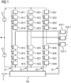
- FIG. 1 is a modular system shown, which is implemented as a modular multipoint power converter.
- a power converter serves, for example, to rectify a three-phase current in a direct current, as is necessary, for example, for HVDC transmissions.
- the illustrated power converter can also be used at the other end of the HVDC line to convert DC into three-phase.
- the system concept of the modular multipoint power converters can also be used for converters.
- the in FIG. 1 reproduced multi-point converter has a variety of modules that are linked together in a string.
- a first strand there are the modules M11 to M18, in a second strand the modules M21 to M28 and in a third strand the modules M31 to M38. All modules usually have the same structure.
- Four of the modules in a string are connected in series with respect to their power path.
- the three module series circuits M11 to M14, M21 to M24 and M31 to M34 are on the one hand connected to the positive rail and on the other hand connected to a respective auxiliary unit AUX1, AUX2 and AUX3.
- the module series circuits M15 to M18, M25 to M28 and M35 to M38 are connected on the one hand to the negative rail and on the other hand to the auxiliary units AUX1, AUX2 and AUX3.
- the power paths of the modules M14 and M15 lead into the auxiliary unit AUX1, the power paths of the modules M24 and M25 in the auxiliary unit AUX2 and the power paths of the modules M34 and M35 in the auxiliary unit AUX3.
- Each of the auxiliary units AUX1, AUX2 and AUX 3 combines the respective power paths and produces one phase of a three-phase system. This would be an inverter realized.
- the power converter can also be designed to convert a three-phase current into a direct current in the reverse direction. In this case it can be used as a rectifier.
- the control of the power converter is done with a control unit MC.
- This control unit MC controls not only all the modules, but also the auxiliary units AUX1, AUX2 and AUX3.
- the modules M11 to M18 are controlled by a first bus B1, the modules M21 to M28 by a second bus B2, the modules M31 to M38 by a third bus B3 and the auxiliary units AUX1 to AUX3 by a fourth bus B4.
- Each of these buses B1 to B4 not only has a data line, but also an auxiliary voltage line. If necessary, bidirectional data is transported via the respective data line.
- the individual modules are supplied with control data by the control unit MC. Eventually, status data such as voltages, temperature values and the like are returned back to the control unit MC.
- both the modules and the auxiliary units are supplied by the control unit MC with an auxiliary voltage which the respective active components need for operation.
- the control unit MC may also have an input E for external commands.
- the power converter of FIG. 1 is purely exemplary.
- the basic structure could also be used for a single-phase converter or a multi-phase converter.
- there must be no symmetrical stress on the DC link so that each leg does not have to be split symmetrically into two as in the example of FIG. 1 , In this case, the auxiliary units AUX1 to AUX3 may then also be omitted.
- the number of modules per strand can also vary.
- FIG. 2 shows the schematic diagram of one of the modules, represented by the module M11 with the essential components here.
- the remaining modules of the system are preferably of the same design.
- switches 1 and 2 are connected in series. These switches 1 and 2 may be circuit breakers and specifically IGBTs.
- the module M11 has two power connections 3 and 4, of which one connection 3 is located at the node between the switches 1 and 2.
- the second power connection 4 is located at the other pole of the second switch 2.
- the contact of the switch 1 facing away from the power connection 3 is connected to the second power connection 4 via a capacitor C, which represents a voltage source of the module.
- the two switches 1 and 2 are controlled by a signal processing device 5. It has a communication connection 6 with which the local signal processing device 5, that is to say the module-internal signal processing device, with a module-external control unit, which in FIG. 2 not shown, can connect in communication.
- the signal processing device 5 preferably receives from the external, central control unit a control value which is converted by the signal processing device 5 into concrete control signals for the switches 1 and 2.
- the signal processing device 5 may be an FPGA or a microprocessor. Both are optionally configured on site to suitably control the module or half-bridge. If necessary, the signal processing device 5 can also be supplied with an auxiliary voltage via the communication connection 6, which requires the active components for operation.
- the control value which the signal processing device 5 receives via the communication connection 6 from the module-external control device, is a voltage-time product value. This value corresponds to a product of a voltage value and a time value.
- the voltage across the capacitor C which also corresponds to the voltage at the power contacts 3 and 4 in the switched-on state, is measured by a voltmeter 7.
- This voltmeter 7 can be integrated into the signal processing device 5 or form a separate measuring device and be coupled to the signal processing device 5 for transmitting the voltage measurement value.
- the capacitor 10 is connected to the power terminals 3 and 4. This means that in this case at the power terminals 3 and 4, the voltage U C is applied, which drops across the capacitor C and which is measured by the voltmeter 7 as a corresponding voltage value. Otherwise, when the switch 1 is opened and the switch 2 is closed, the capacitor C is bypassed, and no voltage is applied to the power terminals 3 and 4.
- the signal processing device 5 knows the current voltage value of the module M11, namely the voltage U C measured at the capacitor C. Moreover, the signal processing device 5 has received from the external control unit via the communication terminal 6 a voltage-time product value for controlling the switches 1 and 2. By dividing the product value by the measured voltage value, the signal processing device 5 receives a time value for the duration in which the switch 1 should be closed and the switch 2 should be open. If appropriate, the time value is also determined in another way from the product value and the voltage value. Eventually, any parasitic effects can be taken into account. For example, the time value can also be determined via a special function or a simple assignment.
- the central control unit supplies as a control value a specific voltage-time product value and a current voltage value U1 is measured.
- the voltage U1 in the switch-on phase would not change between the times t0 and t1 in accordance with a voltage curve u1, and the switch-on time for the switch 1 or the switch-off time for the switch 2 would in the simplest case be the quotient between the product value and the voltage value correspond. In the present example, the time value would be t1.
- the voltage U C changes as a function of time.
- the result is, for example, the voltage curve u2 after the Connection time t0.
- the module voltage U C decreases accordingly below the original value U1.
- the time of the pulse must be extended as its voltage decreases.
- the signal processing device 5 now integrates the measured voltage u2 over the time t until the product value U1 * (t1-t0) has been reached. This is achieved in the present case at time t2. At this time t2, the switch 1 is now opened and the switch 2 is closed, so that the module voltage U C drops to 0.
- the missing in a first pulse voltage-time area is compensated until the next pulse.
- the voltage value under the voltage curve u2 is integrated only between the times t0 and t1.
- the difference of the integral to the product U * (t1-t0), i. the integral under the voltage curve u1 is taken into account only at the next or another subsequent pulse, during which the switch 1 is closed and the switch 2 is opened.
- the necessary voltage-time product values are thus transmitted to the module controller. It is possible to use the local module voltage measurement, whereby a rapid response to voltage changes is possible. Such a rapid response to voltage changes is usually not possible if the measured voltage values would have to be transmitted from the modules to the central control unit.
- each module in addition to the voltage measurement also has a local signal processing device, in particular a controller or FPGA, can now on each module of the delivering PWM value based on the current present Module voltage (DC link voltage of the cell) and the setpoint, namely the voltage-time product value, calculated or determined.
- a local signal processing device in particular a controller or FPGA
- the usually existing anyway measuring device and control logic of a module can be used for the improved module control.
- the local decoupling of the control values to be determined (for example PWM values) from the currently present module voltage results in a better behavior of the overall system. It decouples the effects of fluctuating module voltages from the higher-level current and voltage regulators. This in turn allows a more dynamic adjustment of the required setpoints.
Landscapes
- Engineering & Computer Science (AREA)
- Power Engineering (AREA)
- Inverter Devices (AREA)
Abstract
Description
- Die vorliegende Erfindung betrifft ein modulares, elektronisches System mit mehreren Modulen und einer Steuerungseinheit. Insbesondere bezieht sich die Erfindung auf einen modularen Mehrpunktstromrichter.
- Häufig werden elektronische Systeme modular ausgebaut. Der Grund hierfür kann in der Flexibilität, in der verarbeiteten Leistung, der eingesetzten Spannung etc. liegen.
- Ein konkretes Beispiel sind sogenannte modulare Mehrpunktstromrichter (Modular Multilevel Converter: M2C). Solche modulare Mehrpunktstromrichter können beispielsweise für Hochspannungs-Gleichstrom-Übertragungen (HGÜ) eingesetzt werden. Sie eignen sich aber ebenso für Mittelspannungs- und Niedervoltanwendungen.
- Der modulare Aufbau solcher Systeme bedingt, dass die einzelnen Module in geeigneter Weise angesteuert werden müssen. Dazu kann jedes Modul einzeln mit einem separaten Kabel angesprochen werden. Alternativ hierzu können die Module des Systems aber auch durch einen Kommunikationsbus vernetzt sein. Dieser Bus stellt dann die Schnittstelle zwischen einer zentralen Steuerungseinheit und den einzelnen Modulen dar. Dabei kann jedes Modul in Abhängigkeit von seiner Funktion beziehungsweise seines Aufbaus einen Aktor, eine Zelle oder dergleichen darstellen.
- Jedes Modul wird von der zentralen Steuereinheit mit seinen zu stellenden Sollwerten gesteuert. Ein solcher Sollwert ist beispielsweise der Aussteuergrad des lokalen, d.h. modulseitigen PWM-Modulators (Pulsweitenmodulation) und repräsentiert so in der Regel einen bestimmten Spannungs- oder Stromsollwert. Der konkrete PWM-Wert wird meist auf der Grundlage der zuletzt auf der zentralen Steuereinheit vorhandenen Modulspannung, die jedes Modul selbst liefert, errechnet. Aufgrund reduzierter Kommunikationskapazitäten werden die in der zentralen Steuerungseinheit vorhandenen Modulspannungen, die die Ausgangsspannungen der Module darstellen, bei Bus-vernetzten Systemen mit einer Aktualisierungsfrequenz kleiner/gleich der Modulationsfrequenz erneuert.
- Bei Systemen, deren Module beziehungsweise Steller relativ kleine lokale Energiespeicher besitzen, ergibt sich ein entsprechend hoher Spannungsrippel. Dies führt zu einer Diskrepanz zwischen errechnetem Sollwert und tatsächlich realisierter Ausgangsspannung an jedem Modul.
- Um dieser Problematik zu begegnen, besitzen bisherige Systeme meist eine schnelle parallele Anbindung der Module an die zentrale Steuerungseinheit (Punkt-zu-Punkt-Verbindung) oder sie verfügen über einen ausreichend großen Energiespeicher, welcher einen ausreichend kleinen Spannungsrippel gewährleistet. Beide dieser Alternativen sind jedoch mit erhöhtem Hardwareaufwand verbunden und damit bei kostensensitiven Systemen zu vermeiden.
- Die Aufgabe der vorliegenden Erfindung besteht somit darin, mit möglichst geringem Aufwand die Diskrepanz zwischen Sollwert und Ausgangsspannung bei einem Modul eines modularen Systems zu vermindern.
- Erfindungsgemäß wird diese Aufgabe gelöst durch ein verteiltes, modulares, elektronisches System mit
- mehreren Modulen und
- einer Steuerungseinheit, wobei
- die Steuerungseinheit dazu ausgebildet ist, als Steuerungswerte jeweils Spannungs-Zeit-Produktwerte an die Module zu senden,
- jedes der Module mit
- o einer an- und abschaltbaren Spannungsquelle,
- o einem Spannungsmesser zum Gewinnen mindestens eines Spannungsmesswerts bezüglich der eigenen Ausgangsspannung und
- o einer Signalverarbeitungseinrichtung zum Erzeugen eines Abschaltsignals in Abhängigkeit von dem mindestens einen Spannungsmesswert und dem von der Steuerungseinheit erhaltenen Spannungs-Zeit-Produktwert ausgestattet ist und
- jedes Modul dazu ausgebildet ist, seine Spannungsquelle entsprechend dem erzeugten Abschaltsignal abzuschalten.
- Darüber hinaus wird erfindungsgemäß bereitgestellt ein Verfahren zum Betreiben eines verteilten, modularen, elektronischen Systems mit mehreren Modulen und einer Steuerungseinheit durch
- Senden eines Spannungs-Zeit-Produktwertes als Steuerungswert von der Steuerungseinheit an eines der Module,
- Gewinnen mindestens eines Spannungsmesswerts bezüglich der eigenen Ausgangsspannung und Erzeugen eines Abschaltsignals in Abhängigkeit von dem mindestens einen Spannungsmesswert und dem von der Steuerungseinheit erhaltenen Spannungs-Zeit-Produktwert durch das Modul und
- Abschalten einer Spannungsquelle des Moduls entsprechend dem Abschaltsignal.
- In vorteilhafter Weise sollen entsprechend der Erfindung die einzelnen Module etwas selbständiger betrieben werden, wodurch es gelingt, Soll- und Istzustand bezüglich der Ausgangsspannung aneinander anzugleichen. Hierzu wird anstelle eines reinen Spannungs-Sollwerts ein Spannungs-Zeit-Produktwert als Sollwert beziehungsweise Steuerungswert von der Steuerungseinheit an ein Modul gesendet. Dabei kann natürlich jedes Modul des Systems einen anderen Steuerungswert beziehungsweise Sollwert erhalten. Jedes Modul besitzt eine an- und abschaltbare Spannungsquelle beispielsweise in Form eines Kondensators sowie einen Spannungsmesser, mit dem die Zellspannung des Moduls gemessen werden kann. Da nun jedes Modul seine aktuelle Ausgangsspannung kennt und von der Steuerungseinheit den Spannungs-Zeit-Produktwert, also ein Produkt aus Spannung und Zeit, von der Steuerungseinheit erhalten hat, kann aus beiden Größen ein Zeitwert berechnet oder ein entsprechendes Ausschaltkriterium (z.B. Integral s.u.) gewonnen werden. Der Zeitwert entspräche der Zeitdauer, während der die gemessene Ausgangsspannung anliegen muss. Im einfachsten Fall muss der Spannungs-Zeit-Produktwert einfach durch den gemessenen Spannungswert dividiert werden, um den Zeitwert zu erhalten. Dazu verfügt jedes Modul über eine entsprechende Recheneinrichtung. Der berechnete Zeitwert wird schließlich dazu genutzt, in dem Modul die interne Spannungsquelle abzuschalten. Dadurch kann gewährleistet werden, dass die Sollspannung auch tatsächlich über die gewünschte Zeit vom Modul bereitgestellt wird.
- Vorzugsweise ist das System als modularer Mehrpunktstromrichter ausgebildet. Durch die weitgehende Unabhängigkeit der Module von der Steuerungseinheit im Hinblick auf die Erzeugung der Spannung kann damit erreicht werden, dass der Mehrpunktstromrichter eine Istspannung liefert, die der Sollspannung eher entspricht.
- In einer Ausgestaltung kann das System ein Kommunikationssystem, z.B einen Kommunikationsbus, zur Kommunikation zwischen den Modulen und der Steuerungseinheit aufweisen, über den die Spannungs-Zeit-Produktwerte von der Steuerungseinheit zu den jeweiligen Modulen übertragbar sind. Dies hat den Vorteil, dass die Verschaltung der Module mit der Steuerungseinheit wesentlich einfacher gestaltet werden kann. Insbesondere müssen nicht einzelne Punkt-zu-Punkt-Verbindungen zwischen den Modulen und der Steuerungseinheit aufgebaut werden. Beispielsweise können so sämtliche Module des Systems an einen oder wenige Busse angeschlossen werden.
- In einer weiteren Ausgestaltung kann jedes Modul dazu ausgebildet sein, seine Spannungsquelle durch Pulsweitenmodulation an- und abzuschalten. Dazu verfügt jedes Modul über einen entsprechenden Pulsweitenmodulator, der einen Steuerwert in ein entsprechendes Modulationssignal umsetzt.
- Bei einer Weiterentwicklung werden die Spannungs-Zeit-Produktwerte mit einer geringeren Frequenz aktualisiert als die Modulationsfrequenz der Pulsweitenmodulation. Dies bedeutet, dass eine Spannungs-Zeit-Fläche mit mehreren Impulsen realisiert werden kann/muss. Andererseits kann das aber auch bedeuten, dass die gewünschte Spannungs-Zeit-Fläche entsprechend dem Verhältnis beider Frequenzen zueinander mehrfach wiederholt werden muss. Die modulinterne Steuerung ist entsprechend auszulegen.
- Das modulare System kann für Niederspannungs- und Mittelspannungsbetrieb (mindestens 10 kV) ausgelegt sein. Bei entsprechender Auslegung für höhere Spannungen sind auch Einsätze bei Hochspannungsbetrieb möglich. Beispielsweise können so auch modulare Mehrpunktstromrichter für Hochspannungs-Gleichstrom-Übertragung eingesetzt werden, bei denen Spannungen von 1 Million Volt und mehr auftreten.
- Die Steuerungs- beziehungsweise Recheneinrichtung jedes Moduls kann als FPGA (Field Programmable Gate Array) oder Mikroprozessor realisiert sein. Im Falle eines FPGA kann die Programmierung also beispielsweise vor Ort erfolgen. Beide Recheneinrichtungen ermöglichen eine hohe Flexibilität.
- In einer Ausgestaltungsvariante kann jedes Modul dazu ausgelegt sein, die Dauer eines Impulses, währenddessen die Spannungsquelle angeschaltet ist und währenddessen der Spannungsmesswert gewonnen ist, in Abhängigkeit von dem berechneten Zeitwert einzustellen. Es wird dabei also unmittelbar der aktuelle Impuls und vorzugsweise nur dieser über den Spannungs-Zeit-Produktwert gesteuert. Dies erfordert eine rasche Signalverarbeitung und führt zu einer qualitativ hochwertigen Steuerung.
- Alternativ kann jedes Modul dazu ausgelegt sein, für einen ersten Impuls, währenddessen die Spannungsquelle ausgeschaltet ist, den Spannungsmesswert zu gewinnen und die Dauer eines dem ersten Impuls nachfolgenden Impulses, währenddessen die Spannungsquelle ebenfalls angeschaltet ist, in Abhängigkeit von dem berechneten Zeitwert einzustellen. Dies bedeutet, dass sich ein etwaiges Defizit des ersten Impulses erst auf die Dauer des nachfolgenden zweiten Impulses auswirkt. Gegebenenfalls kann sich ein Defizit auch auf mehrere nachfolgende Impulse auswirken. In diesem Fall kann die Signalverarbeitung unter Umständen eine geringere Geschwindigkeit besitzen.
- Bei einer weiteren alternativen Ausgestaltung ist jedes Modul dazu ausgelegt, kontinuierlich in regelmäßigen Zeitabständen je einen Spannungsmesswert zu gewinnen, die Spannungsmesswerte zu integrieren und das Abschaltsignal zu erzeugen, wenn der Integrationswert den Spannungs-Zeit-Produktwert erreicht oder übersteigt. Damit ist keine Vorhersage für einen Abschaltzeitpunkt notwendig. Vielmehr kann das System sehr dynamisch auf geänderte Spannungsmesswerte reagieren.
- Die oben genannten funktionellen Merkmale des Systems lassen sich auch auf das erfindungsgemäße Verfahren als entsprechende Verfahrensmerkmale übertragen.
- Die vorliegende Erfindung wird nun anhand der beigefügten Zeichnungen näher erläutert, in denen zeigen:
- FIG 1
- die Architektur eines verteilten, modularen, elektronischen Systems anhand eines modularen Mehrpunktstromrichters;
- FIG 2
- einen prinzipiellen Schaltplan eines Moduls des Systems; und
- FIG 3
- einen Spannungsverlauf der Ausgangsspannung an einem Modul.
- Die nachfolgend näher geschilderten Ausführungsbeispiele stellen bevorzugte Ausführungsformen der vorliegenden Erfindung dar. Dabei ist zu beachten, dass die einzelnen Merkmale nicht nur in den geschilderten Kombinationen, sondern auch in Alleinstellung oder in anderen technisch sinnvollen Kombinationen realisierbar sind.
- Ein verteiltes, modulares, elektronisches System weist eine Vielzahl von Modulen und mindestens eine Steuereinheit auf. Die Module sind über einen oder mehrere Kommunikationsbusse mit einer zentralen Steuereinheit verbunden. Derartige verteilte Systeme können im Anlagenbau zahlreiche Anwendungen finden. Dabei kann jedes Modul einen Aktor aufweisen, der eine elektrische oder mechanische Funktionalität besitzt.
- In dem Beispiel von
FIG 1 ist ein modulares System dargestellt, welches als modularer Mehrpunktstromrichter realisiert ist. Ein solcher Stromrichter dient beispielsweise zum Gleichrichten eines Drehstroms in einem Gleichstrom, wie es beispielsweise für HGÜ-Übertragungen notwendig ist. Der dargestellte Stromrichter kann aber auch am anderen Ende der HGÜ-Leitung zum Wandeln von Gleichstrom in Drehstrom eingesetzt werden. Das Systemkonzept der modularen Mehrpunktstromrichter ist aber auch für Umrichter verwendbar. - Der in
FIG 1 wiedergegebene Mehrpunktstromrichter besitzt eine Vielzahl an Modulen, die strangweise miteinander verknüpft sind. In einem ersten Strang befinden sich die Module M11 bis M18, in einem zweiten Strang die Module M21 bis M28 und in einem dritten Strang die Module M31 bis M38. Alle Module besitzen in der Regel gleichen Aufbau. Jeweils vier der Module in einem Strang sind bezogen auf ihren Leistungspfad in Serie geschaltet. - Zwei Gleichspannungsquellen S1 und S2 sind in Serie geschaltet, und durch diese Serienschaltung wird eine Plusschiene "+" und eine Minusschiene "-" symmetrisch mit Gleichspannung gespeist.
- Die drei Modulserienschaltungen M11 bis M14, M21 bis M24 und M31 bis M34 sind einerseits an die Plusschiene angeschlossen und andererseits mit einer jeweiligen Hilfseinheit AUX1, AUX2 und AUX3 verbunden. Symmetrisch dazu sind die Modulserienschaltungen M15 bis M18, M25 bis M28 und M35 bis M38 einerseits mit der Minusschiene verbunden und andererseits mit den Hilfseinheiten AUX1, AUX2 und AUX3. Konkret führen also die Leistungspfade der Module M14 und M15 in die Hilfseinheit AUX1, die Leistungspfade der Module M24 und M25 in die Hilfseinheit AUX2 und die Leistungspfade der Module M34 und M35 in die Hilfseinheit AUX3. Jede der Hilfseinheiten AUX1, AUX2 und AUX 3 vereint die jeweiligen Leistungspfade und produziert eine Phase eines Drehstromsystems. Damit wäre ein Wechselrichter realisiert.
- Alternativ kann der Stromrichter auch dazu ausgebildet sein, dass er in umgekehrter Richtung einen dreiphasigen Strom in einen Gleichstrom wandelt. In diesem Fall kann er als Gleichrichter genutzt werden.
- Die Steuerung des Stromrichters erfolgt mit einer Steuereinheit MC. Diese Steuereinheit MC steuert nicht nur sämtliche Module, sondern auch die Hilfseinheiten AUX1, AUX2 und AUX3. Mit einem ersten Bus B1 werden die Module M11 bis M18, mit einem zweiten Bus B2 die Module M21 bis M28, mit einem dritten Bus B3 die Module M31 bis M38 und mit einem vierten Bus B4 die Hilfseinheiten AUX1 bis AUX3 gesteuert. Jeder dieser Busse B1 bis B4 verfügt nicht nur über eine Datenleitung, sondern auch über eine Hilfsspannungsleitung. Über die jeweilige Datenleitung werden gegebenenfalls bidirektional Daten transportiert. Ebenfalls werden die einzelnen Module von der Steuereinheit MC mit Steuerdaten versorgt. Gegebenenfalls werden Zustandsdaten wie etwa Spannungen, Temperaturwerte und dergleichen, zurück an die Steuereinheit MC geliefert.
- Über die Hilfsspannungsleitungen der Busse B1 bis B4 werden sowohl die Module als auch die Hilfseinheiten von der Steuereinheit MC mit einer Hilfsspannung versorgt, die die jeweiligen aktiven Bauelemente für den Betrieb brauchen. Die Steuereinheit MC besitzt gegebenenfalls noch einen Eingang E für externe Befehle.
- Der Stromrichter von
FIG 1 ist rein exemplarisch. Der prinzipielle Aufbau könnte auch für einen einphasigen Stromrichter oder einen mehrphasigen Stromrichter genutzt werden. Auch muss an den Zwischenkreis nicht eine symmetrische Spannung vorliegen, sodass jeder Strang nicht symmetrisch zweigeteilt sein muss wie in dem Beispiel vonFIG 1 . In diesem Fall können dann auch gegebenenfalls die Hilfseinheiten AUX1 bis AUX3 entfallen. Auch die Anzahl der Module pro Strang kann variieren. -
FIG 2 zeigt den prinzipiellen Schaltplan eines der Module, stellvertretend anhand des Moduls M11 mit den hier wesentlichen Bauelementen. Die übrigen Module des Systems sind vorzugsweise gleich aufgebaut. - In einer Halbbrücke sind zwei Schalter 1 und 2 in Serie geschaltet. Bei diesen Schaltern 1 und 2 kann es sich um Leistungsschalter und speziell um IGBTs handeln. Das Modul M11 verfügt über zwei Leistungsanschlüsse 3 und 4, von denen der eine Anschluss 3 am Knoten zwischen den Schaltern 1 und 2 liegt. Der zweite Leistungsanschluss 4 liegt am anderen Pol des zweiten Schalters 2.
- Der dem Leistungsanschluss 3 abgewandte Kontakt des Schalters 1 ist über einen Kondensator C, der eine Spannungsquelle des Moduls darstellt, an den zweiten Leistungsanschluss 4 gelegt.
- Die beiden Schalter 1 und 2 werden von einer Signalverarbeitungseinrichtung 5 gesteuert. Sie besitzt einen Kommunikationsanschluss 6, mit dem die lokale Signalverarbeitungseinrichtung 5, das heißt die modulinterne Signalverarbeitungseinrichtung, mit einer modulexternen Steuerungseinheit, die in
FIG 2 nicht dargestellt ist, in Kommunikationsverbindung treten kann. Vorzugsweise erhält die Signalverarbeitungseinrichtung 5 von der externen, zentralen Steuerungseinheit einen Steuerungswert, der von der Signalverarbeitungseinrichtung 5 in konkrete Steuerungssignale für die Schalter 1 und 2 umgesetzt wird. - Bei der Signalverarbeitungseinrichtung 5 kann es sich um ein FPGA oder einen Mikroprozessor handeln. Beide werden gegebenenfalls vor Ort konfiguriert, um das Modul beziehungsweise die Halbbrücke in geeigneter Weise zu steuern. Über den Kommunikationsanschluss 6 kann die Signalverarbeitungseinrichtung 5 gegebenenfalls auch mit einer Hilfsspannung versorgt werden, die die aktiven Bauelemente zum Betrieb benötigen.
- Bei dem Steuerwert, den die Signalverarbeitungseinrichtung 5 über den Kommunikationsanschluss 6 von der modulexternen Steuerungseinrichtung erhält, handelt es sich um einen Spannungs-Zeit-Produktwert. Dieser Wert entspricht also einem Produkt eines Spannungswerts und eines Zeitwerts.
- Darüber hinaus wird die Spannung an dem Kondensator C, die im eingeschalteten Zustand auch der Spannung an den Leistungskontakten 3 und 4 entspricht, durch einen Spannungsmesser 7 gemessen. Dieser Spannungsmesser 7 kann in die Signalverarbeitungseinrichtung 5 integriert sein oder eine separate Messeinrichtung bilden und mit der Signalverarbeitungseinrichtung 5 zur Übertragung des Spannungsmesswerts gekoppelt sein.
- Nachfolgend wird die Funktion des Moduls genauer im Detail erläutert. Ist der Schalter 1 geschlossen und der Schalter 2 geöffnet, so ist der Kondensator 10 an die Leistungsanschlüsse 3 und 4 angeschlossen. Dies bedeutet, dass in diesem Fall an den Leistungsanschlüssen 3 und 4 die Spannung UC anliegt, die über den Kondensator C abfällt und die von dem Spannungsmesser 7 als entsprechender Spannungswert gemessen wird. Andernfalls, wenn der Schalter 1 geöffnet und der Schalter 2 geschlossen ist, ist der Kondensator C überbrückt, und an den Leistungsanschlüssen 3 und 4 liegt keine Spannung an.
- Die Signalverarbeitungseinrichtung 5 kennt den aktuellen Spannungswert des Moduls M11, nämlich die am Kondensator C gemessene Spannung UC. Darüber hinaus hat die Signalverarbeitungseinrichtung 5 von der externen Steuerungseinheit über den Kommunikationsanschluss 6 einen Spannungs-Zeit-Produktwert zur Steuerung der Schalter 1 und 2 erhalten. Aus beiden Werten ermittelt die Signalverarbeitungseinrichtung 5 nun die Schaltzeiten der Schalter 1 und 2. Durch Division des Produktwerts durch den gemessenen Spannungswert erhält die Signalverarbeitungseinrichtung 5 einen Zeitwert für die Dauer, in der der Schalter 1 geschlossen und der Schalter 2 geöffnet sein sollte. Gegebenenfalls wird der Zeitwert auch auf eine andere Weise aus dem Produktwert und dem Spannungswert ermittelt. Eventuell können so etwaige parasitäre Effekte berücksichtigt werden. So kann der Zeitwert beispielsweise auch über eine spezielle Funktion oder eine einfache Zuordnung ermittelt werden.
- Im Zusammenhang mit
FIG 3 kann die Wirkungsweise der Schaltung vonFIG 2 besser erfasst werden. Die zentrale Steuerungseinheit liefert als Steuerwert einen bestimmten Spannungs-Zeit-Produktwert und es wird ein aktueller Spannungswert U1 gemessen. Bei idealen Bauelementen würde sich die Spannung U1 in der Einschaltphase zwischen den Zeitpunkten t0 und t1 entsprechend einem Spannungsverlauf u1 nicht ändern, und die Einschaltzeit für den Schalter 1 beziehungsweise die Ausschaltzeit für den Schalter 2 würde im einfachsten Fall dem Quotienten zwischen dem Produktwert und dem Spannungswert entsprechen. Im vorliegenden Beispiel wäre der Zeitwert t1. - Da das Modul jedoch aus realen Bauelementen besteht beziehungsweise einer realen Beschaltung unterworfen ist, verändert sich die Spannung UC in Abhängigkeit von der Zeit. Es ergibt sich beispielsweise der Spannungsverlauf u2 nach dem Anschaltzeitpunkt t0. Die Modulspannung UC sinkt demnach unter den ursprünglichen Wert U1 ab. Da jedoch das Modul von der zentralen Steuerungseinheit als Sollwert den Produktwert U1*(t1-t0) erhalten hat, muss die Zeit des Impulses verlängert werden, da seine Spannung sinkt.
- In einem Ausführungsbeispiel integriert nun die Signalverarbeitungseinrichtung 5 die gemessene Spannung u2 über der Zeit t so lange auf, bis der Produktwert U1*(t1-t0) erreicht ist. Dies ist im vorliegenden Fall zum Zeitpunkt t2 erreicht. Zu diesem Zeitpunkt t2 wird nun der Schalter 1 geöffnet und der Schalter 2 geschlossen, sodass die Modulspannung UC auf 0 sinkt.
- In einem anderen Ausführungsbeispiel wird die bei einem ersten Impuls fehlende Spannungs-Zeit-Fläche erst beim nächsten Impuls ausgeglichen. So wird beispielsweise der Spannungswert unter dem Spannungsverlauf u2 nur zwischen den Zeitpunkten t0 und t1 integriert. Die Differenz des Integrals zu dem Produkt U*(t1-t0), d.h. dem Integral unter dem Spannungsverlauf u1, wird erst beim nächsten oder einem anderen folgenden Impuls, während dessen der Schalter 1 geschlossen und der Schalter 2 geöffnet ist, berücksichtigt.
- Anstatt die zu stellenden PWM-Werte von der zentralen Steuerungseinrichtung zu den einzelnen Modulen zu übertragen, werden also die notwendigen Spannungs-Zeit-Produktwerte zur Modulsteuerung übertragen. Dabei kann man sich der lokalen Modulspannungsmessung bedienen, wodurch eine rasche Reaktion auf Spannungsänderungen möglich ist. Eine derart rasche Reaktion auf Spannungsänderungen ist in der Regel nicht möglich, wenn die gemessenen Spannungswerte erst von den Modulen zu der zentralen Steuerungseinheit übertragen werden müssten.
- Da jedes Modul neben der Spannungsmessung auch über eine lokale Signalverarbeitungseinrichtung, insbesondere einen Controller oder FPGA, verfügt, kann nun auf jedem Modul der zustellende PWM-Wert auf Grundlage der aktuelle vorliegenden Modulspannung (Zwischenkreisspannung der Zelle) und des Sollwerts, nämlich des Spannungs-Zeit-Produktwerts, errechnet beziehungsweise bestimmt werden.
- In vorteilhafter Weise kann für die verbesserte Modulsteuerung die in der Regel ohnehin vorhandene Messeinrichtung und Ansteuerlogik eines Moduls genutzt werden. Durch die lokale Entkopplung der zu ermittelnden Steuerwerte (z.B. PWM-Werte) von der aktuell vorhandenen Modulspannung ergibt sich ein besseres Verhalten des Gesamtsystems. Es entkoppelt die Einflüsse schwankender Modulspannungen von den übergeordneten Strom- und Spannungsreglern. Dies wiederum ermöglicht ein dynamischeres Einregeln der geforderten Sollwerte.
Claims (10)
- Verteiltes, modulares, elektronisches System mit- mehreren Modulen (M11 bis M18, M21 bis M28, M31 bis M38) und- einer Steuerungseinheit (MC),dadurch gekennzeichnet, dass- die Steuerungseinheit (MC) dazu ausgebildet ist, als Steuerungswerte jeweils Spannungs-Zeit-Produktwerte an die Module zu senden,- jedes der Module (M11 bis M18, M21 bis M28, M31 bis M38) mito einer an- und abschaltbaren Spannungsquelle (C),o einem Spannungsmesser (7) zum Gewinnen mindestens eines Spannungsmesswerts (U1) bezüglich der eigenen Ausgangsspannung undo einer Signalverarbeitungseinrichtung (5) zum Erzeugen eines Abschaltsignals in Abhängigkeit von dem mindestens einen Spannungsmesswert (U1) und dem von der Steuerungseinheit (MC) erhaltenen Spannungs-Zeit-Produktwert ausgestattet ist und- jedes Modul (M11 bis M18, M21 bis M28, M31 bis M38) dazu ausgebildet ist, seine Spannungsquelle (S1, S2) entsprechend dem erzeugten Abschaltsignal abzuschalten.
- System nach Anspruch 1, das als modularer Mehrpunktstromrichter ausgebildet ist.
- System nach Anspruch 1 oder 2, das ein Kommuniktionssystem (B1 bis B4) zur Kommunikation zwischen den Modulen (M11 bis M18, M21 bis M28, M31 bis M38) und der Steuerungseinheit (MC) aufweist, über den die Spannungs-Zeit-Produktwerte von der Steuerungseinheit (MC) zu den jeweiligen Modulen (M11 bis M18, M21 bis M28, M31 bis M38) übertragbar sind.
- System nach einem der vorhergehenden Ansprüche, wobei jedes Modul (M11 bis M18, M21 bis M28, M31 bis M38) dazu ausgebildet ist, seine Spannungsquelle (C) durch Pulsweitenmodulation an- und abzuschalten.
- System nach Anspruch 4, wobei die Spannungs-Zeit-Produktwerte mit einer geringeren Frequenz aktualisiert werden als die Modulationsfrequenz der Pulsweitenmodulation.
- System nach einem der vorhergehenden Ansprüche, das für Niederspannung unter 1kV ausgelegt ist.
- System nach einem der vorhergehenden Ansprüche, wobei die Signalverarbeitungseinrichtung (5) dazu ausgelegt ist, für das Abschaltsignal einen Zeitwert (tl) zu bestimmen.
- System nach Anspruch 7, wobei jedes Modul (M11 bis M18, M21 bis M28, M31 bis M38) dazu ausgelegt ist, für einen ersten Impuls, während dessen die Spannungsquelle (C) angeschaltet ist, den Spannungsmesswert (U1) zu gewinnen und die Dauer eines dem ersten Impuls nachfolgenden zweiten Impulses, während dessen die Spannungsquelle (C) ebenfalls angeschaltet ist, in Abhängigkeit von dem bestimmten Zeitwert einzustellen.
- System nach einem der Ansprüche 1 bis 6, wobei jedes Modul (M11 bis M18, M21 bis M28, M31 bis M38) dazu ausgelegt ist, kontinuierlich (u2) in regelmäßigen Zeitabständen je einen Spannungsmesswert zu gewinnen, die Spannungsmesswerte zu integrieren und das Abschaltsignal zu erzeugen, wenn der Integrationswert den Spannungs-Zeit-Produktwert erreicht oder übersteigt.
- Verfahren zum Betreiben eines verteilten, modularen, elektronischen Systems mit mehreren Modulen (M11 bis M18, M21 bis M28, M31 bis M38) und einer Steuerungseinheit (MC), gekennzeichnet durch- Senden eines Spannungs-Zeit-Produktwertes als Steuerungswert von der Steuerungseinheit (MC) an eines der Module,- Gewinnen mindestens eines Spannungsmesswerts (U1) bezüglich der eigenen Ausgangsspannung und Erzeugen eines Abschaltsignals in Abhängigkeit von dem mindestens einen Spannungsmesswert und dem von der Steuerungseinheit (MC) erhaltenen Spannungs-Zeit-Produktwert durch das Modul und- Abschalten einer Spannungsquelle des Moduls (M11 bis M18, M21 bis M28, M31 bis M38) entsprechend dem Abschaltsignal.
Priority Applications (3)
| Application Number | Priority Date | Filing Date | Title |
|---|---|---|---|
| PL16156307T PL3208930T3 (pl) | 2016-02-18 | 2016-02-18 | Modułowy przetwornik wielokomorowy z wewnątrzkomórkową kompensacją odchyleń napięciowych na kondensatorze ogniwa |
| EP16156307.7A EP3208930B1 (de) | 2016-02-18 | 2016-02-18 | Modularer mehrzellenumrichter mit zellinterner kompensation von spannungsschwankungen am zellkondensator |
| PCT/EP2016/078951 WO2017140393A1 (de) | 2016-02-18 | 2016-11-28 | Modularer mehrzellenumrichter mit zellinterner kompensation von spannungsschwankungen am zellkondensator |
Applications Claiming Priority (1)
| Application Number | Priority Date | Filing Date | Title |
|---|---|---|---|
| EP16156307.7A EP3208930B1 (de) | 2016-02-18 | 2016-02-18 | Modularer mehrzellenumrichter mit zellinterner kompensation von spannungsschwankungen am zellkondensator |
Publications (2)
| Publication Number | Publication Date |
|---|---|
| EP3208930A1 true EP3208930A1 (de) | 2017-08-23 |
| EP3208930B1 EP3208930B1 (de) | 2020-08-12 |
Family
ID=55442655
Family Applications (1)
| Application Number | Title | Priority Date | Filing Date |
|---|---|---|---|
| EP16156307.7A Active EP3208930B1 (de) | 2016-02-18 | 2016-02-18 | Modularer mehrzellenumrichter mit zellinterner kompensation von spannungsschwankungen am zellkondensator |
Country Status (3)
| Country | Link |
|---|---|
| EP (1) | EP3208930B1 (de) |
| PL (1) | PL3208930T3 (de) |
| WO (1) | WO2017140393A1 (de) |
Citations (1)
| Publication number | Priority date | Publication date | Assignee | Title |
|---|---|---|---|---|
| EP2458726A1 (de) * | 2009-07-21 | 2012-05-30 | Hitachi, Ltd. | Stromwandler |
-
2016
- 2016-02-18 PL PL16156307T patent/PL3208930T3/pl unknown
- 2016-02-18 EP EP16156307.7A patent/EP3208930B1/de active Active
- 2016-11-28 WO PCT/EP2016/078951 patent/WO2017140393A1/de not_active Ceased
Patent Citations (1)
| Publication number | Priority date | Publication date | Assignee | Title |
|---|---|---|---|---|
| EP2458726A1 (de) * | 2009-07-21 | 2012-05-30 | Hitachi, Ltd. | Stromwandler |
Non-Patent Citations (2)
| Title |
|---|
| JOSE IGNACIO LEON ET AL: "Multidimensional Modulation Technique for Cascaded Multilevel Converters", IEEE TRANSACTIONS ON INDUSTRIAL ELECTRONICS, IEEE SERVICE CENTER, PISCATAWAY, NJ, USA, vol. 58, no. 2, 1 February 2011 (2011-02-01), pages 412 - 420, XP011341642, ISSN: 0278-0046, DOI: 10.1109/TIE.2010.2048833 * |
| SAMIR KOURO ET AL: "Multicarrier PWM With DC-Link Ripple Feedforward Compensation for Multilevel Inverters", IEEE TRANSACTIONS ON POWER ELECTRONICS, INSTITUTE OF ELECTRICAL AND ELECTRONICS ENGINEERS, USA, vol. 23, no. 1, 1 January 2008 (2008-01-01), pages 52 - 59, XP011198648, ISSN: 0885-8993, DOI: 10.1109/TPEL.2007.911834 * |
Also Published As
| Publication number | Publication date |
|---|---|
| EP3208930B1 (de) | 2020-08-12 |
| PL3208930T3 (pl) | 2021-01-25 |
| WO2017140393A1 (de) | 2017-08-24 |
Similar Documents
| Publication | Publication Date | Title |
|---|---|---|
| EP1927183B1 (de) | Verfahren zur steuerung eines mehrphasigen stromrichters mit verteilten energiespeichern | |
| EP3333005A1 (de) | Modulare leistungselektronik zum laden eines elektrisch betriebenen fahrzeugs | |
| EP3172821B1 (de) | Leistungselektronisches system zum betreiben einer last und verfahren zur synchronisation von leistungsmodulen | |
| WO1999041816A1 (de) | Vorrichtung und verfahren zum gesteuerten parallelbetrieb von gleichspannungswandlern | |
| DE102008032813A1 (de) | Netzanbindung von Solarzellen | |
| EP2654190A2 (de) | Verfahren zum Betreiben einer elektrischen Schaltung | |
| EP2494688B1 (de) | Verfahren zum betrieb einer umrichterschaltung sowie vorrichtung zur durchführung des verfahrens | |
| EP3151413A1 (de) | Steuervorrichtung und steuerverfahren für grosse stromrichter | |
| EP2807738B1 (de) | Multizellenkonverter | |
| WO2010049185A1 (de) | Anordnung und verfahren zur phasenanschnitt-steuerung | |
| EP3220527B1 (de) | Modularer mehrstufenumrichter | |
| DE102019105196B4 (de) | Verfahren zur Strombegrenzung bei transienten Spannungsänderungen an einem Wechselstromausgang eines Multilevel-Wechselrichters und Multilevel-Wechselrichter | |
| EP3208930B1 (de) | Modularer mehrzellenumrichter mit zellinterner kompensation von spannungsschwankungen am zellkondensator | |
| EP3363091B1 (de) | Vorrichtung und verfahren zum steuern eines lastflusses in einem wechselspannungsnetz | |
| DE102013109714A1 (de) | Verfahren zum Betreiben einer elektrischen Schaltung sowie elektrische Schaltung | |
| DE102020112723B4 (de) | Wechselrichter mit drei Brückenzweigen und Verfahren zum Betreiben eines derartigen Wechselrichters | |
| WO2013186006A2 (de) | Multizellenkonverter | |
| WO2014095233A2 (de) | Batterie mit mindestens einem batteriestrang sowie verfahren zur regelung einer batteriespannung | |
| EP3590770B1 (de) | Vorrichtung zum ansteuern eines elektrischen verbrauchers in einem fahrzeug-bordnetz und bordnetz eines fahrzeugs | |
| WO2023025715A1 (de) | Schaltungsanordnung und verfahren zur erzeugung einer wechselspannung | |
| EP1053588B1 (de) | Verfahren zur erstellung von stellbefehlen für stromrichter | |
| EP3331118B1 (de) | Anlage zum übertragen elektrischer leistung | |
| WO2022144138A1 (de) | Flying capacitor modul und multilevel-umrichter | |
| EP2928055B1 (de) | Modularer Stromrichter und Verfahren zur Erzeugung einer sinusförmigen Ausgangsspannung mit reduziertem Oberschwingungsgehalt | |
| DE102020208092A1 (de) | Verfahren und Vorrichtung zum Entladen eines Zwischenkreiskondensators |
Legal Events
| Date | Code | Title | Description |
|---|---|---|---|
| PUAI | Public reference made under article 153(3) epc to a published international application that has entered the european phase |
Free format text: ORIGINAL CODE: 0009012 |
|
| STAA | Information on the status of an ep patent application or granted ep patent |
Free format text: STATUS: THE APPLICATION HAS BEEN PUBLISHED |
|
| AK | Designated contracting states |
Kind code of ref document: A1 Designated state(s): AL AT BE BG CH CY CZ DE DK EE ES FI FR GB GR HR HU IE IS IT LI LT LU LV MC MK MT NL NO PL PT RO RS SE SI SK SM TR |
|
| AX | Request for extension of the european patent |
Extension state: BA ME |
|
| RAP1 | Party data changed (applicant data changed or rights of an application transferred) |
Owner name: SIEMENS AKTIENGESELLSCHAFT |
|
| STAA | Information on the status of an ep patent application or granted ep patent |
Free format text: STATUS: REQUEST FOR EXAMINATION WAS MADE |
|
| 17P | Request for examination filed |
Effective date: 20180222 |
|
| RBV | Designated contracting states (corrected) |
Designated state(s): AL AT BE BG CH CY CZ DE DK EE ES FI FR GB GR HR HU IE IS IT LI LT LU LV MC MK MT NL NO PL PT RO RS SE SI SK SM TR |
|
| GRAP | Despatch of communication of intention to grant a patent |
Free format text: ORIGINAL CODE: EPIDOSNIGR1 |
|
| STAA | Information on the status of an ep patent application or granted ep patent |
Free format text: STATUS: GRANT OF PATENT IS INTENDED |
|
| INTG | Intention to grant announced |
Effective date: 20200409 |
|
| GRAS | Grant fee paid |
Free format text: ORIGINAL CODE: EPIDOSNIGR3 |
|
| GRAA | (expected) grant |
Free format text: ORIGINAL CODE: 0009210 |
|
| STAA | Information on the status of an ep patent application or granted ep patent |
Free format text: STATUS: THE PATENT HAS BEEN GRANTED |
|
| AK | Designated contracting states |
Kind code of ref document: B1 Designated state(s): AL AT BE BG CH CY CZ DE DK EE ES FI FR GB GR HR HU IE IS IT LI LT LU LV MC MK MT NL NO PL PT RO RS SE SI SK SM TR |
|
| REG | Reference to a national code |
Ref country code: CH Ref legal event code: EP |
|
| REG | Reference to a national code |
Ref country code: IE Ref legal event code: FG4D Free format text: LANGUAGE OF EP DOCUMENT: GERMAN |
|
| REG | Reference to a national code |
Ref country code: DE Ref legal event code: R096 Ref document number: 502016010792 Country of ref document: DE |
|
| REG | Reference to a national code |
Ref country code: AT Ref legal event code: REF Ref document number: 1302541 Country of ref document: AT Kind code of ref document: T Effective date: 20200915 |
|
| REG | Reference to a national code |
Ref country code: CH Ref legal event code: NV Representative=s name: SIEMENS SCHWEIZ AG, CH |
|
| REG | Reference to a national code |
Ref country code: SE Ref legal event code: TRGR |
|
| REG | Reference to a national code |
Ref country code: DE Ref legal event code: R081 Ref document number: 502016010792 Country of ref document: DE Owner name: SIEMENS ENERGY GLOBAL GMBH & CO. KG, DE Free format text: FORMER OWNER: SIEMENS AKTIENGESELLSCHAFT, 80333 MUENCHEN, DE |
|
| REG | Reference to a national code |
Ref country code: LT Ref legal event code: MG4D |
|
| REG | Reference to a national code |
Ref country code: NL Ref legal event code: MP Effective date: 20200812 |
|
| RAP2 | Party data changed (patent owner data changed or rights of a patent transferred) |
Owner name: SIEMENS ENERGY GLOBAL GMBH & CO. KG |
|
| PG25 | Lapsed in a contracting state [announced via postgrant information from national office to epo] |
Ref country code: BG Free format text: LAPSE BECAUSE OF FAILURE TO SUBMIT A TRANSLATION OF THE DESCRIPTION OR TO PAY THE FEE WITHIN THE PRESCRIBED TIME-LIMIT Effective date: 20201112 Ref country code: GR Free format text: LAPSE BECAUSE OF FAILURE TO SUBMIT A TRANSLATION OF THE DESCRIPTION OR TO PAY THE FEE WITHIN THE PRESCRIBED TIME-LIMIT Effective date: 20201113 Ref country code: NO Free format text: LAPSE BECAUSE OF FAILURE TO SUBMIT A TRANSLATION OF THE DESCRIPTION OR TO PAY THE FEE WITHIN THE PRESCRIBED TIME-LIMIT Effective date: 20201112 Ref country code: FI Free format text: LAPSE BECAUSE OF FAILURE TO SUBMIT A TRANSLATION OF THE DESCRIPTION OR TO PAY THE FEE WITHIN THE PRESCRIBED TIME-LIMIT Effective date: 20200812 Ref country code: HR Free format text: LAPSE BECAUSE OF FAILURE TO SUBMIT A TRANSLATION OF THE DESCRIPTION OR TO PAY THE FEE WITHIN THE PRESCRIBED TIME-LIMIT Effective date: 20200812 Ref country code: LT Free format text: LAPSE BECAUSE OF FAILURE TO SUBMIT A TRANSLATION OF THE DESCRIPTION OR TO PAY THE FEE WITHIN THE PRESCRIBED TIME-LIMIT Effective date: 20200812 |
|
| PG25 | Lapsed in a contracting state [announced via postgrant information from national office to epo] |
Ref country code: IS Free format text: LAPSE BECAUSE OF FAILURE TO SUBMIT A TRANSLATION OF THE DESCRIPTION OR TO PAY THE FEE WITHIN THE PRESCRIBED TIME-LIMIT Effective date: 20201212 Ref country code: LV Free format text: LAPSE BECAUSE OF FAILURE TO SUBMIT A TRANSLATION OF THE DESCRIPTION OR TO PAY THE FEE WITHIN THE PRESCRIBED TIME-LIMIT Effective date: 20200812 Ref country code: RS Free format text: LAPSE BECAUSE OF FAILURE TO SUBMIT A TRANSLATION OF THE DESCRIPTION OR TO PAY THE FEE WITHIN THE PRESCRIBED TIME-LIMIT Effective date: 20200812 Ref country code: NL Free format text: LAPSE BECAUSE OF FAILURE TO SUBMIT A TRANSLATION OF THE DESCRIPTION OR TO PAY THE FEE WITHIN THE PRESCRIBED TIME-LIMIT Effective date: 20200812 |
|
| PG25 | Lapsed in a contracting state [announced via postgrant information from national office to epo] |
Ref country code: EE Free format text: LAPSE BECAUSE OF FAILURE TO SUBMIT A TRANSLATION OF THE DESCRIPTION OR TO PAY THE FEE WITHIN THE PRESCRIBED TIME-LIMIT Effective date: 20200812 Ref country code: RO Free format text: LAPSE BECAUSE OF FAILURE TO SUBMIT A TRANSLATION OF THE DESCRIPTION OR TO PAY THE FEE WITHIN THE PRESCRIBED TIME-LIMIT Effective date: 20200812 Ref country code: SM Free format text: LAPSE BECAUSE OF FAILURE TO SUBMIT A TRANSLATION OF THE DESCRIPTION OR TO PAY THE FEE WITHIN THE PRESCRIBED TIME-LIMIT Effective date: 20200812 Ref country code: CZ Free format text: LAPSE BECAUSE OF FAILURE TO SUBMIT A TRANSLATION OF THE DESCRIPTION OR TO PAY THE FEE WITHIN THE PRESCRIBED TIME-LIMIT Effective date: 20200812 Ref country code: DK Free format text: LAPSE BECAUSE OF FAILURE TO SUBMIT A TRANSLATION OF THE DESCRIPTION OR TO PAY THE FEE WITHIN THE PRESCRIBED TIME-LIMIT Effective date: 20200812 |
|
| REG | Reference to a national code |
Ref country code: DE Ref legal event code: R097 Ref document number: 502016010792 Country of ref document: DE |
|
| PG25 | Lapsed in a contracting state [announced via postgrant information from national office to epo] |
Ref country code: AL Free format text: LAPSE BECAUSE OF FAILURE TO SUBMIT A TRANSLATION OF THE DESCRIPTION OR TO PAY THE FEE WITHIN THE PRESCRIBED TIME-LIMIT Effective date: 20200812 Ref country code: ES Free format text: LAPSE BECAUSE OF FAILURE TO SUBMIT A TRANSLATION OF THE DESCRIPTION OR TO PAY THE FEE WITHIN THE PRESCRIBED TIME-LIMIT Effective date: 20200812 |
|
| PLBE | No opposition filed within time limit |
Free format text: ORIGINAL CODE: 0009261 |
|
| STAA | Information on the status of an ep patent application or granted ep patent |
Free format text: STATUS: NO OPPOSITION FILED WITHIN TIME LIMIT |
|
| PG25 | Lapsed in a contracting state [announced via postgrant information from national office to epo] |
Ref country code: SK Free format text: LAPSE BECAUSE OF FAILURE TO SUBMIT A TRANSLATION OF THE DESCRIPTION OR TO PAY THE FEE WITHIN THE PRESCRIBED TIME-LIMIT Effective date: 20200812 |
|
| 26N | No opposition filed |
Effective date: 20210514 |
|
| PG25 | Lapsed in a contracting state [announced via postgrant information from national office to epo] |
Ref country code: SI Free format text: LAPSE BECAUSE OF FAILURE TO SUBMIT A TRANSLATION OF THE DESCRIPTION OR TO PAY THE FEE WITHIN THE PRESCRIBED TIME-LIMIT Effective date: 20200812 |
|
| PG25 | Lapsed in a contracting state [announced via postgrant information from national office to epo] |
Ref country code: MC Free format text: LAPSE BECAUSE OF FAILURE TO SUBMIT A TRANSLATION OF THE DESCRIPTION OR TO PAY THE FEE WITHIN THE PRESCRIBED TIME-LIMIT Effective date: 20200812 |
|
| REG | Reference to a national code |
Ref country code: BE Ref legal event code: MM Effective date: 20210228 |
|
| PG25 | Lapsed in a contracting state [announced via postgrant information from national office to epo] |
Ref country code: LU Free format text: LAPSE BECAUSE OF NON-PAYMENT OF DUE FEES Effective date: 20210218 |
|
| REG | Reference to a national code |
Ref country code: GB Ref legal event code: 732E Free format text: REGISTERED BETWEEN 20211202 AND 20211209 |
|
| PG25 | Lapsed in a contracting state [announced via postgrant information from national office to epo] |
Ref country code: IE Free format text: LAPSE BECAUSE OF NON-PAYMENT OF DUE FEES Effective date: 20210218 |
|
| REG | Reference to a national code |
Ref country code: AT Ref legal event code: MM01 Ref document number: 1302541 Country of ref document: AT Kind code of ref document: T Effective date: 20210218 |
|
| PG25 | Lapsed in a contracting state [announced via postgrant information from national office to epo] |
Ref country code: AT Free format text: LAPSE BECAUSE OF NON-PAYMENT OF DUE FEES Effective date: 20210218 |
|
| PG25 | Lapsed in a contracting state [announced via postgrant information from national office to epo] |
Ref country code: BE Free format text: LAPSE BECAUSE OF NON-PAYMENT OF DUE FEES Effective date: 20210228 |
|
| PG25 | Lapsed in a contracting state [announced via postgrant information from national office to epo] |
Ref country code: PT Free format text: LAPSE BECAUSE OF FAILURE TO SUBMIT A TRANSLATION OF THE DESCRIPTION OR TO PAY THE FEE WITHIN THE PRESCRIBED TIME-LIMIT Effective date: 20201214 |
|
| PG25 | Lapsed in a contracting state [announced via postgrant information from national office to epo] |
Ref country code: HU Free format text: LAPSE BECAUSE OF FAILURE TO SUBMIT A TRANSLATION OF THE DESCRIPTION OR TO PAY THE FEE WITHIN THE PRESCRIBED TIME-LIMIT; INVALID AB INITIO Effective date: 20160218 |
|
| PG25 | Lapsed in a contracting state [announced via postgrant information from national office to epo] |
Ref country code: CY Free format text: LAPSE BECAUSE OF FAILURE TO SUBMIT A TRANSLATION OF THE DESCRIPTION OR TO PAY THE FEE WITHIN THE PRESCRIBED TIME-LIMIT Effective date: 20200812 |
|
| P01 | Opt-out of the competence of the unified patent court (upc) registered |
Effective date: 20231222 |
|
| PG25 | Lapsed in a contracting state [announced via postgrant information from national office to epo] |
Ref country code: MK Free format text: LAPSE BECAUSE OF FAILURE TO SUBMIT A TRANSLATION OF THE DESCRIPTION OR TO PAY THE FEE WITHIN THE PRESCRIBED TIME-LIMIT Effective date: 20200812 |
|
| PG25 | Lapsed in a contracting state [announced via postgrant information from national office to epo] |
Ref country code: MT Free format text: LAPSE BECAUSE OF FAILURE TO SUBMIT A TRANSLATION OF THE DESCRIPTION OR TO PAY THE FEE WITHIN THE PRESCRIBED TIME-LIMIT Effective date: 20200812 |
|
| PG25 | Lapsed in a contracting state [announced via postgrant information from national office to epo] |
Ref country code: TR Free format text: LAPSE BECAUSE OF FAILURE TO SUBMIT A TRANSLATION OF THE DESCRIPTION OR TO PAY THE FEE WITHIN THE PRESCRIBED TIME-LIMIT Effective date: 20200812 |
|
| REG | Reference to a national code |
Ref country code: CH Ref legal event code: U11 Free format text: ST27 STATUS EVENT CODE: U-0-0-U10-U11 (AS PROVIDED BY THE NATIONAL OFFICE) Effective date: 20260301 |
|
| PGFP | Annual fee paid to national office [announced via postgrant information from national office to epo] |
Ref country code: SE Payment date: 20260223 Year of fee payment: 11 |
|
| PGFP | Annual fee paid to national office [announced via postgrant information from national office to epo] |
Ref country code: GB Payment date: 20260223 Year of fee payment: 11 |
|
| PGFP | Annual fee paid to national office [announced via postgrant information from national office to epo] |
Ref country code: DE Payment date: 20260220 Year of fee payment: 11 |
|
| PGFP | Annual fee paid to national office [announced via postgrant information from national office to epo] |
Ref country code: IT Payment date: 20260220 Year of fee payment: 11 |
|
| PGFP | Annual fee paid to national office [announced via postgrant information from national office to epo] |
Ref country code: FR Payment date: 20260224 Year of fee payment: 11 |
|
| PGFP | Annual fee paid to national office [announced via postgrant information from national office to epo] |
Ref country code: CH Payment date: 20260301 Year of fee payment: 11 |
|
| PGFP | Annual fee paid to national office [announced via postgrant information from national office to epo] |
Ref country code: PL Payment date: 20260126 Year of fee payment: 11 |