EP3208830A1 - A method to improve ge channel interfacial layer quality for cmos finfet - Google Patents
A method to improve ge channel interfacial layer quality for cmos finfet Download PDFInfo
- Publication number
- EP3208830A1 EP3208830A1 EP17156218.4A EP17156218A EP3208830A1 EP 3208830 A1 EP3208830 A1 EP 3208830A1 EP 17156218 A EP17156218 A EP 17156218A EP 3208830 A1 EP3208830 A1 EP 3208830A1
- Authority
- EP
- European Patent Office
- Prior art keywords
- layer
- dummy gate
- germanium
- fins
- germanium layer
- Prior art date
- Legal status (The legal status is an assumption and is not a legal conclusion. Google has not performed a legal analysis and makes no representation as to the accuracy of the status listed.)
- Withdrawn
Links
Images



Classifications
-
- H—ELECTRICITY
- H10—SEMICONDUCTOR DEVICES; ELECTRIC SOLID-STATE DEVICES NOT OTHERWISE PROVIDED FOR
- H10D—INORGANIC ELECTRIC SEMICONDUCTOR DEVICES
- H10D30/00—Field-effect transistors [FET]
- H10D30/01—Manufacture or treatment
- H10D30/021—Manufacture or treatment of FETs having insulated gates [IGFET]
- H10D30/024—Manufacture or treatment of FETs having insulated gates [IGFET] of fin field-effect transistors [FinFET]
- H10D30/0241—Manufacture or treatment of FETs having insulated gates [IGFET] of fin field-effect transistors [FinFET] doping of vertical sidewalls, e.g. using tilted or multi-angled implants
-
- H—ELECTRICITY
- H10—SEMICONDUCTOR DEVICES; ELECTRIC SOLID-STATE DEVICES NOT OTHERWISE PROVIDED FOR
- H10D—INORGANIC ELECTRIC SEMICONDUCTOR DEVICES
- H10D30/00—Field-effect transistors [FET]
- H10D30/60—Insulated-gate field-effect transistors [IGFET]
- H10D30/62—Fin field-effect transistors [FinFET]
- H10D30/6215—Fin field-effect transistors [FinFET] having multiple independently-addressable gate electrodes
-
- H—ELECTRICITY
- H10—SEMICONDUCTOR DEVICES; ELECTRIC SOLID-STATE DEVICES NOT OTHERWISE PROVIDED FOR
- H10D—INORGANIC ELECTRIC SEMICONDUCTOR DEVICES
- H10D30/00—Field-effect transistors [FET]
- H10D30/01—Manufacture or treatment
- H10D30/021—Manufacture or treatment of FETs having insulated gates [IGFET]
- H10D30/024—Manufacture or treatment of FETs having insulated gates [IGFET] of fin field-effect transistors [FinFET]
-
- H—ELECTRICITY
- H10—SEMICONDUCTOR DEVICES; ELECTRIC SOLID-STATE DEVICES NOT OTHERWISE PROVIDED FOR
- H10D—INORGANIC ELECTRIC SEMICONDUCTOR DEVICES
- H10D30/00—Field-effect transistors [FET]
- H10D30/60—Insulated-gate field-effect transistors [IGFET]
- H10D30/62—Fin field-effect transistors [FinFET]
-
- H—ELECTRICITY
- H10—SEMICONDUCTOR DEVICES; ELECTRIC SOLID-STATE DEVICES NOT OTHERWISE PROVIDED FOR
- H10D—INORGANIC ELECTRIC SEMICONDUCTOR DEVICES
- H10D30/00—Field-effect transistors [FET]
- H10D30/60—Insulated-gate field-effect transistors [IGFET]
- H10D30/751—Insulated-gate field-effect transistors [IGFET] having composition variations in the channel regions
-
- H—ELECTRICITY
- H10—SEMICONDUCTOR DEVICES; ELECTRIC SOLID-STATE DEVICES NOT OTHERWISE PROVIDED FOR
- H10D—INORGANIC ELECTRIC SEMICONDUCTOR DEVICES
- H10D30/00—Field-effect transistors [FET]
- H10D30/60—Insulated-gate field-effect transistors [IGFET]
- H10D30/791—Arrangements for exerting mechanical stress on the crystal lattice of the channel regions
- H10D30/797—Arrangements for exerting mechanical stress on the crystal lattice of the channel regions being in source or drain regions, e.g. SiGe source or drain
-
- H—ELECTRICITY
- H10—SEMICONDUCTOR DEVICES; ELECTRIC SOLID-STATE DEVICES NOT OTHERWISE PROVIDED FOR
- H10D—INORGANIC ELECTRIC SEMICONDUCTOR DEVICES
- H10D62/00—Semiconductor bodies, or regions thereof, of devices having potential barriers
- H10D62/80—Semiconductor bodies, or regions thereof, of devices having potential barriers characterised by the materials
- H10D62/82—Heterojunctions
- H10D62/822—Heterojunctions comprising only Group IV materials heterojunctions, e.g. Si/Ge heterojunctions
-
- H—ELECTRICITY
- H10—SEMICONDUCTOR DEVICES; ELECTRIC SOLID-STATE DEVICES NOT OTHERWISE PROVIDED FOR
- H10D—INORGANIC ELECTRIC SEMICONDUCTOR DEVICES
- H10D64/00—Electrodes of devices having potential barriers
- H10D64/01—Manufacture or treatment
- H10D64/013—Manufacture or treatment of electrodes having a conductor capacitively coupled to a semiconductor by an insulator
- H10D64/01356—Manufacture or treatment of electrodes having a conductor capacitively coupled to a semiconductor by an insulator the insulator being formed after the semiconductor body, the semiconductor being a Group IV material and not being silicon, e.g. Ge, SiGe or SiGeC
-
- H—ELECTRICITY
- H10—SEMICONDUCTOR DEVICES; ELECTRIC SOLID-STATE DEVICES NOT OTHERWISE PROVIDED FOR
- H10D—INORGANIC ELECTRIC SEMICONDUCTOR DEVICES
- H10D64/00—Electrodes of devices having potential barriers
- H10D64/01—Manufacture or treatment
- H10D64/017—Manufacture or treatment using dummy gates in processes wherein at least parts of the final gates are self-aligned to the dummy gates, i.e. replacement gate processes
-
- H—ELECTRICITY
- H10—SEMICONDUCTOR DEVICES; ELECTRIC SOLID-STATE DEVICES NOT OTHERWISE PROVIDED FOR
- H10D—INORGANIC ELECTRIC SEMICONDUCTOR DEVICES
- H10D64/00—Electrodes of devices having potential barriers
- H10D64/01—Manufacture or treatment
- H10D64/021—Manufacture or treatment using multiple gate spacer layers, e.g. bilayered sidewall spacers
-
- H—ELECTRICITY
- H10—SEMICONDUCTOR DEVICES; ELECTRIC SOLID-STATE DEVICES NOT OTHERWISE PROVIDED FOR
- H10D—INORGANIC ELECTRIC SEMICONDUCTOR DEVICES
- H10D64/00—Electrodes of devices having potential barriers
- H10D64/20—Electrodes characterised by their shapes, relative sizes or dispositions
- H10D64/27—Electrodes not carrying the current to be rectified, amplified, oscillated or switched, e.g. gates
-
- H—ELECTRICITY
- H10—SEMICONDUCTOR DEVICES; ELECTRIC SOLID-STATE DEVICES NOT OTHERWISE PROVIDED FOR
- H10D—INORGANIC ELECTRIC SEMICONDUCTOR DEVICES
- H10D64/00—Electrodes of devices having potential barriers
- H10D64/20—Electrodes characterised by their shapes, relative sizes or dispositions
- H10D64/27—Electrodes not carrying the current to be rectified, amplified, oscillated or switched, e.g. gates
- H10D64/311—Gate electrodes for field-effect devices
- H10D64/411—Gate electrodes for field-effect devices for FETs
- H10D64/511—Gate electrodes for field-effect devices for FETs for IGFETs
- H10D64/512—Disposition of the gate electrodes, e.g. buried gates
-
- H—ELECTRICITY
- H10—SEMICONDUCTOR DEVICES; ELECTRIC SOLID-STATE DEVICES NOT OTHERWISE PROVIDED FOR
- H10D—INORGANIC ELECTRIC SEMICONDUCTOR DEVICES
- H10D64/00—Electrodes of devices having potential barriers
- H10D64/60—Electrodes characterised by their materials
- H10D64/66—Electrodes having a conductor capacitively coupled to a semiconductor by an insulator, e.g. MIS electrodes
- H10D64/68—Electrodes having a conductor capacitively coupled to a semiconductor by an insulator, e.g. MIS electrodes characterised by the insulator, e.g. by the gate insulator
-
- H—ELECTRICITY
- H10—SEMICONDUCTOR DEVICES; ELECTRIC SOLID-STATE DEVICES NOT OTHERWISE PROVIDED FOR
- H10D—INORGANIC ELECTRIC SEMICONDUCTOR DEVICES
- H10D64/00—Electrodes of devices having potential barriers
- H10D64/60—Electrodes characterised by their materials
- H10D64/66—Electrodes having a conductor capacitively coupled to a semiconductor by an insulator, e.g. MIS electrodes
- H10D64/68—Electrodes having a conductor capacitively coupled to a semiconductor by an insulator, e.g. MIS electrodes characterised by the insulator, e.g. by the gate insulator
- H10D64/681—Electrodes having a conductor capacitively coupled to a semiconductor by an insulator, e.g. MIS electrodes characterised by the insulator, e.g. by the gate insulator having a compositional variation, e.g. multilayered
- H10D64/685—Electrodes having a conductor capacitively coupled to a semiconductor by an insulator, e.g. MIS electrodes characterised by the insulator, e.g. by the gate insulator having a compositional variation, e.g. multilayered being perpendicular to the channel plane
-
- H—ELECTRICITY
- H10—SEMICONDUCTOR DEVICES; ELECTRIC SOLID-STATE DEVICES NOT OTHERWISE PROVIDED FOR
- H10D—INORGANIC ELECTRIC SEMICONDUCTOR DEVICES
- H10D64/00—Electrodes of devices having potential barriers
- H10D64/60—Electrodes characterised by their materials
- H10D64/66—Electrodes having a conductor capacitively coupled to a semiconductor by an insulator, e.g. MIS electrodes
- H10D64/68—Electrodes having a conductor capacitively coupled to a semiconductor by an insulator, e.g. MIS electrodes characterised by the insulator, e.g. by the gate insulator
- H10D64/693—Electrodes having a conductor capacitively coupled to a semiconductor by an insulator, e.g. MIS electrodes characterised by the insulator, e.g. by the gate insulator the insulator comprising nitrogen, e.g. nitrides, oxynitrides or nitrogen-doped materials
-
- H—ELECTRICITY
- H10—SEMICONDUCTOR DEVICES; ELECTRIC SOLID-STATE DEVICES NOT OTHERWISE PROVIDED FOR
- H10D—INORGANIC ELECTRIC SEMICONDUCTOR DEVICES
- H10D84/00—Integrated devices formed in or on semiconductor substrates that comprise only semiconducting layers, e.g. on Si wafers or on GaAs-on-Si wafers
- H10D84/01—Manufacture or treatment
- H10D84/0123—Integrating together multiple components covered by H10D12/00 or H10D30/00, e.g. integrating multiple IGBTs
- H10D84/0126—Integrating together multiple components covered by H10D12/00 or H10D30/00, e.g. integrating multiple IGBTs the components including insulated gates, e.g. IGFETs
- H10D84/0165—Integrating together multiple components covered by H10D12/00 or H10D30/00, e.g. integrating multiple IGBTs the components including insulated gates, e.g. IGFETs the components including complementary IGFETs, e.g. CMOS devices
- H10D84/0193—Integrating together multiple components covered by H10D12/00 or H10D30/00, e.g. integrating multiple IGBTs the components including insulated gates, e.g. IGFETs the components including complementary IGFETs, e.g. CMOS devices the components including FinFETs
-
- H—ELECTRICITY
- H10—SEMICONDUCTOR DEVICES; ELECTRIC SOLID-STATE DEVICES NOT OTHERWISE PROVIDED FOR
- H10D—INORGANIC ELECTRIC SEMICONDUCTOR DEVICES
- H10D84/00—Integrated devices formed in or on semiconductor substrates that comprise only semiconducting layers, e.g. on Si wafers or on GaAs-on-Si wafers
- H10D84/01—Manufacture or treatment
- H10D84/02—Manufacture or treatment characterised by using material-based technologies
- H10D84/03—Manufacture or treatment characterised by using material-based technologies using Group IV technology, e.g. silicon technology or silicon-carbide [SiC] technology
- H10D84/038—Manufacture or treatment characterised by using material-based technologies using Group IV technology, e.g. silicon technology or silicon-carbide [SiC] technology using silicon technology, e.g. SiGe
-
- H—ELECTRICITY
- H10—SEMICONDUCTOR DEVICES; ELECTRIC SOLID-STATE DEVICES NOT OTHERWISE PROVIDED FOR
- H10P—GENERIC PROCESSES OR APPARATUS FOR THE MANUFACTURE OR TREATMENT OF DEVICES COVERED BY CLASS H10
- H10P14/00—Formation of materials, e.g. in the shape of layers or pillars
- H10P14/60—Formation of materials, e.g. in the shape of layers or pillars of insulating materials
- H10P14/63—Formation of materials, e.g. in the shape of layers or pillars of insulating materials characterised by the formation processes
- H10P14/6302—Non-deposition formation processes
- H10P14/6304—Formation by oxidation, e.g. oxidation of the substrate
- H10P14/6306—Formation by oxidation, e.g. oxidation of the substrate of the semiconductor materials
- H10P14/6308—Formation by oxidation, e.g. oxidation of the substrate of the semiconductor materials of Group IV semiconductors
-
- H—ELECTRICITY
- H10—SEMICONDUCTOR DEVICES; ELECTRIC SOLID-STATE DEVICES NOT OTHERWISE PROVIDED FOR
- H10P—GENERIC PROCESSES OR APPARATUS FOR THE MANUFACTURE OR TREATMENT OF DEVICES COVERED BY CLASS H10
- H10P14/00—Formation of materials, e.g. in the shape of layers or pillars
- H10P14/60—Formation of materials, e.g. in the shape of layers or pillars of insulating materials
- H10P14/65—Formation of materials, e.g. in the shape of layers or pillars of insulating materials characterised by treatments performed before or after the formation of the materials
- H10P14/6516—Formation of materials, e.g. in the shape of layers or pillars of insulating materials characterised by treatments performed before or after the formation of the materials of treatments performed after formation of the materials
- H10P14/6518—Formation of materials, e.g. in the shape of layers or pillars of insulating materials characterised by treatments performed before or after the formation of the materials of treatments performed after formation of the materials by introduction of substances into an already-existing insulating layer
- H10P14/6519—Formation of materials, e.g. in the shape of layers or pillars of insulating materials characterised by treatments performed before or after the formation of the materials of treatments performed after formation of the materials by introduction of substances into an already-existing insulating layer the substance being oxygen
-
- H—ELECTRICITY
- H10—SEMICONDUCTOR DEVICES; ELECTRIC SOLID-STATE DEVICES NOT OTHERWISE PROVIDED FOR
- H10P—GENERIC PROCESSES OR APPARATUS FOR THE MANUFACTURE OR TREATMENT OF DEVICES COVERED BY CLASS H10
- H10P14/00—Formation of materials, e.g. in the shape of layers or pillars
- H10P14/60—Formation of materials, e.g. in the shape of layers or pillars of insulating materials
- H10P14/65—Formation of materials, e.g. in the shape of layers or pillars of insulating materials characterised by treatments performed before or after the formation of the materials
- H10P14/6516—Formation of materials, e.g. in the shape of layers or pillars of insulating materials characterised by treatments performed before or after the formation of the materials of treatments performed after formation of the materials
- H10P14/6518—Formation of materials, e.g. in the shape of layers or pillars of insulating materials characterised by treatments performed before or after the formation of the materials of treatments performed after formation of the materials by introduction of substances into an already-existing insulating layer
- H10P14/6524—Formation of materials, e.g. in the shape of layers or pillars of insulating materials characterised by treatments performed before or after the formation of the materials of treatments performed after formation of the materials by introduction of substances into an already-existing insulating layer the substance being nitrogen
- H10P14/6526—Formation of materials, e.g. in the shape of layers or pillars of insulating materials characterised by treatments performed before or after the formation of the materials of treatments performed after formation of the materials by introduction of substances into an already-existing insulating layer the substance being nitrogen introduced into an oxide material, e.g. changing SiO to SiON
-
- H—ELECTRICITY
- H10—SEMICONDUCTOR DEVICES; ELECTRIC SOLID-STATE DEVICES NOT OTHERWISE PROVIDED FOR
- H10P—GENERIC PROCESSES OR APPARATUS FOR THE MANUFACTURE OR TREATMENT OF DEVICES COVERED BY CLASS H10
- H10P32/00—Diffusion of dopants within, into or out of wafers, substrates or parts of devices
- H10P32/10—Diffusion of dopants within, into or out of semiconductor bodies or layers
- H10P32/12—Diffusion of dopants within, into or out of semiconductor bodies or layers between a solid phase and a gaseous phase
-
- H—ELECTRICITY
- H10—SEMICONDUCTOR DEVICES; ELECTRIC SOLID-STATE DEVICES NOT OTHERWISE PROVIDED FOR
- H10P—GENERIC PROCESSES OR APPARATUS FOR THE MANUFACTURE OR TREATMENT OF DEVICES COVERED BY CLASS H10
- H10P32/00—Diffusion of dopants within, into or out of wafers, substrates or parts of devices
- H10P32/10—Diffusion of dopants within, into or out of semiconductor bodies or layers
- H10P32/17—Diffusion of dopants within, into or out of semiconductor bodies or layers characterised by the semiconductor material
- H10P32/171—Diffusion of dopants within, into or out of semiconductor bodies or layers characterised by the semiconductor material being group IV material
Definitions
- Embodiments of the present invention relate to the field of semiconductor device fabrication.
- embodiments of the disclosure relate to a fin field effect transistor device having improved hot carrier reliability and method for manufacturing the same.
- high-mobility materials e.g., for forming a channel or channel region
- high-k dielectric materials e.g., for forming a channel or channel region
- GaAs, InP, InGaAs, InAs, and GaSb have high electron mobility
- Ge has a relatively high hole mobility
- these materials can be used for the channel of MOS transistor devices.
- the interface between the high-k dielectric layer and the high mobility substrate may affect the device performance and reliability.
- the present invention provides a semiconductor device that has an improved interface between the high mobility channel materials and the high-k dielectric for obtaining higher reliability.
- a method for manufacturing the semiconductor device is also provided.
- a first aspect of the present invention provides a method for manufacturing a semiconductor device.
- the method includes: providing a semiconductor structure, which includes a substrate structure containing a substrate, a plurality of fins, a germanium layer on the top surface of the fins, a dummy gate structure on the germanium layer and including a dummy gate insulating material on the germanium layer, a dummy gate on the dummy gate insulating material, and a hardmask on the dummy gate, and spacers on opposite sides of the dummy gate structure and on a portion of the germanium layer.
- the method also includes: forming an interlayer dielectric layer on the substrate structure covering the dummy gate structure, planarizing the interlayer dielectric layer to expose a surface of the dummy gate, removing the dummy gate and the dummy gate insulating material to expose a surface of the germanium layer, performing a silane impregnation process on the exposed surface of the germanium layer to introduce silicon to the germanium layer, and performing a first oxidation process on the germanium layer to form an oxide layer comprising silicon and germanium.
- the method may further include: forming a source region and a drain region adjacent to the opposite sides of the germanium layer.
- the source region and the drain region comprise SiGe or SiP.
- the fins include a silicon layer below the germanium layer.
- the silane impregnation process is performed by immersing the semiconductor structure in an atmosphere comprising silane for a time duration between 1 minute and 30 minutes, at a temperature in a range between 400 °C and 500 °C, and under a pressure in a range between 5 Torr and 20 Torr.
- the oxide layer includes SiO 2 , GeO 2 , and SiGeO 2 .
- the method also includes performing a nitration process on the oxide layer to form a nitrogen-containing oxide layer.
- the nitration process includes the use of ammonia, nitrous oxide, nitric oxide, or nitrogen plasma.
- the method further includes forming a high-k dielectric layer on the nitrogen-containing oxide layer and on sidewalls of the spacers.
- the method also includes forming a high-k dielectric layer on the oxide layer and on sidewalls of the spacers.
- the method further includes performing a second oxidation process on the high-k dielectric layer to reduce vacancies in the high-k dielectric layer.
- the second oxidation process is performed in an atmosphere comprising oxygen at a temperature in a range between 450°C and 550 °C, and an oxygen concentration less than 10 ppm.
- the method further includes forming a gate electrode on the high-k dielectric layer.
- the fins include a first set of fins configured to form first type devices and a second set of fins configured to form second type devices.
- the method further includes forming a dielectric layer on the substrate structure, wherein the fins protrude from the dielectric layer.
- providing the semiconductor structure includes: providing an initial structure comprising the substrate structure, the plurality of fins protruding from the substrate structure and containing a semiconductor layer, forming an initial germanium layer, forming a dummy gate insulating layer on the initial germanium layer, a dummy gate material layer on the dummy gate insulating layer, and a hardmask layer on the dummy gate material layer, removing a portion of the hardmask layer, a portion of the dummy gate material layer, and a portion of the dummy gate insulating layer to form a dummy gate structure, forming spacers on sidewalls of the dummy gate structure, and removing a portion of the initial germanium layer and a portion of the semiconductor layer by etching using the dummy gate structure and the spacers as a mask.
- the germanium layer is disposed on a top surface and lateral surfaces of each of the fins in the transverse direction.
- a second aspect of the present invention provides a semiconductor device that includes: a substrate structure having a substrate, a plurality of fins each protruding from the substrate structure, a germanium layer on a top surface of the fins, spacers on opposite sides of the germanium layer, an oxide layer on a surface of the germanium layer between the spacers, the oxide layer comprising silicon and germanium, a high-k dielectric layer on the oxide layer and on inner sidewalls of the spacers, and a gate electrode on the high-k dielectric layer.
- the oxide layer is a nitrogen-containing oxide layer.
- the semiconductor device further includes a source region and a drain region adjacent opposite sides of the germanium layer.
- the fins include a silicon layer below the germanium layer.
- the fins may include a first set of fins for forming first type transistor devices and a second set of fins for forming second type transistor devices.
- the substrate structure also includes a dielectric layer on the substrate, and the fins protrude from the dielectric layer.
- the oxide layer, the high-k dielectric layer and the gate electrode are above the dielectric layer.
- the source region and the drain region include silicon germanium (SiGe) or silicon phosphorus (SiP).
- the semiconductor device includes: an interlayer dielectric layer surrounding the spacers, the high-k dielectric layer, and the gate electrode.
- the germanium layer may be disposed on a top surface and lateral surfaces of each of the fins in the transverse direction.
- a semiconductor device according to the second aspect of the present invention may be obtained by a method according to the second aspect of the present invention.
- first, second, third, etc. do not denote any order, but rather the terms first, second, third, etc. are used to distinguish one element from another.
- use of the terms a, an, etc. does not denote a limitation of quantity, but rather denote the presence of at least one of the referenced items.
- substrate may include any structure having an exposed surface with which to form an integrated circuit.
- substrate' is understood to include semiconductor wafers and is also used to refer to semiconductor structures during processing and may include other layers that have been fabricated thereupon.
- a “substrate” may include doped and undoped semiconductor wafers, epitaxial semiconductor layers, as well as other semiconductor structures.
- FIG. 1 is a flowchart illustrating a method for manufacturing a semiconductor device.
- FIGS. 2 through 10 are cross-sectional views of intermediate stages of the manufacturing method according to some embodiments of the present invention.
- each drawing or block in the flowchart represents a process associated with embodiments of the method described. Those of skill in the art will recognize that additional blocks and drawings that described the embodiments may be added.
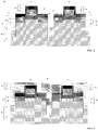
- FIG. 2 is a cross-sectional view illustrating a semiconductor substrate 20 according to some embodiments of the present invention.
- semiconductor substrate 20 may include a substrate structure 30 having a substrate (e.g., silicon) 31, a plurality of fins 40 protruding from substrate structure 30. Fins 40 each include a germanium layer 41 on the top surface.
- Semiconductor substrate 20 may further include a dummy gate structure 50 on germanium layer 41.
- Dummy gate structure 50 includes a dummy gate insulating material (e.g., silicon dioxide) 51 on germanium layer 41, a dummy gate (e.g., polysilicon) 52 on dummy gate insulating material 51, and a hardmask (e.g., silicon nitride) 53 on dummy gate 52.
- Semiconductor substrate 20 may also include spacers 56 disposed on opposite sides of dummy gate structure 50 and adjacent to a source region and a drain region, respectively. Spacers 56 cover the remaining portion of the surface of germanium layer 41 that is not covered by dummy gate structure 50. Spacers 56 may include one or more layers of oxide and nitride.
- cross-sectional view shown in FIG. 2 is a cross section of the fins along the longitudinal direction (i.e., lengthwise cross-sectional view); the cross-section of the fins including the germanium layer along the transverse direction (i.e., cross-wise direction) are best shown in FIG. 11B . It will be noted that for a better understanding, the manufacturing method of a semiconductor device will be described in detail in conjunction with FIGS. 11A through 11E .
- each of the fins include a germanium layer 41 disposed on the surface of the fins along the cross-section in the transverse (cross-wise) direction, as shown in FIG. 11B .
- each of the fins includes a silicon layer 42 below the germanium layer 41, as shown in FIG. 2 .
- fins 40 may include a first set of fins 91 configured to form first type devices (e.g., NMOS transistors) and a second set of fins 92 configured to form second type devices (e.g., PMOS devices), as shown in FIG. 2 .
- first type devices e.g., NMOS transistors
- second type devices e.g., PMOS devices
- substrate structure 30 may also include a dielectric layer (e.g., silicon dioxide) 32 on substrate 31.
- a dielectric layer e.g., silicon dioxide
- the fins protrude from dielectric layer 32, and dummy gate insulating material 51 and dummy gate 52 are above dielectric layer 32.
- fin refers to a vertical structure protruding from the substrate structure, which includes the substrate or the substrate and the dielectric layer disposed thereon, however, the term “fin” may also refer broadly as the fin structure of a FinFET device.
- semiconductor structure 20 also includes a source region and a drain region adjacent to germanium layer 41.
- semiconductor structure 20 in the first set of fins 91, semiconductor structure 20 includes a first source region 61 and a first drain region 62 on opposite sides of and adjacent to germanium layer 41.
- semiconductor structure 20 in the second set of fins 92, semiconductor structure 20 includes a second source region 71 and a second drain region 72 on opposite sides of and adjacent to germanium layer 41.
- the source and drain regions include silicon germanium (SiGe) or silicon phosphorus (SiP) to apply stress to the channel region.
- first source and drain regions 61, 62 include SiP
- second source and drain regions 71, 72 include SiGe. It is understood that the source and drain regions can be epitaxially grown from silicon layer 42, and in-situ doped during the growth process.
- first source region 61 may include a heavily doped region 63
- first drain region 62 may include a heavily doped region 64
- Second source region 71 may include a heavily doped region 73
- second drain region 72 may include a heavily doped region 74.
- an interlayer dielectric layer is formed on the substrate structure to cover the dummy gate structure.
- FIG. 3 is a cross-sectional view illustrating an intermediate structure according to block S102.
- an interlayer dielectric layer 45 is formed, e.g., by deposition, on the substrate structure 30 to cover the dummy gate structure 50.
- interlayer dielectric layer 45 includes silicon dioxide.
- a planarization process is performed on the interlayer dielectric layer to expose a surface of the dummy gate.
- FIG. 4 is a cross-sectional view illustrating an intermediate structure according to block S103.
- a planarization (e.g., chemical mechanical polishing) process is performed on the interlayer dielectric layer to expose a surface of dummy gate 52.
- the dummy gate and the dummy gate insulating material are removed to expose a surface of the germanium layer.
- FIG. 5 is a cross-sectional view illustrating an intermediate structure according to block S104. As shown in FIG. 5 , dummy gate 52 and dummy gate insulating material 51 are removed to expose a surface of germanium layer 41.
- the exposed surface of the germanium layer is impregnated with silane to introduce silicon atoms into the germanium layer.
- FIG. 6 is a cross-sectional view illustrating an intermediate structure according to block S105. As shown in FIG. 6 , the exposed surface of germanium layer 41 is impregnated with silane to introduce silicon atoms into the germanium layer to form a first surface layer 47 comprising silicon and germanium.
- the silane impregnation process may be performed at a temperature between 400 degrees C and 500 degrees C, preferably 450 degrees C, the semiconductor structure is immersed in a silane atmosphere between 1 minutes and 30 minutes (e.g., 5, 10, or 20 minutes), and under a pressure of 5 Torr to 20 Torr, preferably 10 Torr. Silicon (silane) may be absorbed on the surface of the germanium layer, or into the surface of the germanium layer at a depth within about 1 nm.
- a first oxidation process is performed on the exposed surface of the silicon absorbed germanium layer to form an oxide layer comprising silicon and germanium elements.
- FIG. 7 is a cross-sectional view illustrating an intermediate structure according to block S106.
- a first oxidation process is performed on the exposed surface of first surface layer 47 to form an oxide layer 49, oxide layer 49 includes silicon and germanium.
- Oxide layer 49 may include silicon oxide and germanium oxide, including but not limited to SiO 2 , GeO 2 , and SiGeO 2 .
- the first oxidation process may be performed using an in-situ steam generation (ISSG) process or rapid thermal oxidation (RTO) process.
- ISSG in-situ steam generation
- RTO rapid thermal oxidation
- the oxide layer has a thickness of 10 angstroms to 40 angstroms.
- a method for manufacturing a semiconductor device has been provided by embodiments of the present invention.
- the above-described method can reduce defects in the surface of the germanium layer of a fin, reduce the defect density, thereby improving the performance and reliability of the thus manufactured semiconductor device.
- the method may further include performing a nitridation process on oxide layer 49 to form a nitrogen-containing oxide layer 81.
- the nitridation process may be performed using ammonia (NH 3 ), nitrous oxide (N 2 O), nitric oxide (NO), or nitrogen plasma.
- the nitridation process can improve the film characteristics of the oxide layer by reducing the equivalent oxide thickness (EOT) of the oxide layer, and further improving the characteristics of the interface between the germanium layer and the oxide layer (nitrogen-containing oxide layer), thereby further improving the performance and reliability of the semiconductor device.
- EOT equivalent oxide thickness
- the method may also include forming a high-k dielectric layer 83 on nitrogen-containing oxide layer 81 and inner sidewalls of spacers 56.
- the inner sidewalls of the spacers refer to the sidewalls facing the trench or facing the gate or dummy gate.
- the high-k dielectric layer may be formed on the oxide layer and the sidewalls of the spacers. That is, the high-k dielectric layer is formed on the oxide layer prior to the nitridation and the sidewalls of the spacers.
- the method according to the present invention may further include performing a second oxidation process on high-k dielectric layer 83, in order to reduce vacancies in the high-k dielectric layer.
- the second oxidation process is performed in an atmosphere comprising oxygen, at a temperature in the range between 450°C and 550°C, preferably at 500 °C.
- the oxygen concentration may be less than 10 ppm.
- the method may further include forming a gate 85 on the high-k dielectric layer.
- the gate is a conductive gate.
- the gate may include a metal gate and a conductive functional layer disposed between the metal gate and the high-k dielectric layer.
- the conductive functional layer may be a TaN buffer layer, a work-function adjusting layer, etc.
- the metal gate may include copper or aluminum.
- the conductive functional layer (if present) and the gate material layer may be firstly deposited on the structure shown in FIG. 10 , then a planarization (e.g., CMP) process is performed on the gate material layer to form the gate.
- CMP planarization
- embodiments of the present invention further provide a method for manufacturing a semiconductor device, which can reduce the defect density of the oxide layer and vacancies in the high-k dielectric layer, thereby improving the semiconductor device reliability.
- FIGS. 11A through 11F are cross-sectional views of intermediate structures of a method for manufacturing a semiconductor device according to some embodiments of the present invention.
- Initial structure 100 may include a substrate structure 30, and a plurality of initial fins including a semiconductor layer 42.
- the semiconductor layer may include a silicon layer, a silicon germanium layer, or other similar semiconductor materials layer.
- Substrate structure 30 includes a substrate (e.g. silicon) 31.
- the substrate structure may further include a dielectric layer (e.g., silicon dioxide) 32 on substrate 31.
- the fins protrude from dielectric layer 32, as shown in FIG. 11A .
- substrate 31 is shown as a bulk silicon-based substrate herein, the present invention is not limited thereto.
- substrate 31 may be a silicon on insulator (SOI) substrate.
- the fins may be formed on the buried oxide layer (insulating layer), so that dielectric layer 32 is not required.
- the fins may include a first set of fins 91 configured to form first type devices (e.g., NMOS transistors) and a second set of fins 92 configured to form second type devices (e.g., PMOS transistors), as shown in FIG. 11A .
- first type devices e.g., NMOS transistors
- second type devices e.g., PMOS transistors
- an initial germanium layer 41 is formed on semiconductor layer 42, as shown in FIG. 11B .
- initial germanium layer 41 may be formed on semiconductor layer 42 using an epitaxial growth process, as shown in FIG. 11B .
- the semiconductor layer may include a silicon layer
- the epitaxial growth process may be performed on the silicon layer in a mixed gas of silane and germane
- the concentration ratio of silane and germane gas is controlled in order to reduce the silane concentration with time, i.e., increasing the germane content and decreasing the silane content until the silane content is reduced to zero to form the initial germanium layer 41. It is, however, understood that the initial germanium layer can be formed using other processes.
- a dummy gate insulating layer 51 is formed on germanium layer 41, a dummy gate material layer 52 is formed on dummy gate insulating layer 51, and a hardmask layer 53 is formed on dummy gate material layer 52, as shown in FIG. 11C .
- dummy gate insulating layer 51 is formed using a deposition process on initial germanium layer 41
- dummy gate material layer 52 is formed using a deposition process on dummy gate insulating layer 51
- hardmask layer 53 is formed using a deposition process on dummy gate material layer 52.
- Dummy gate structure 50 includes a dummy gate insulating material 51, a dummy gate 52, and a hardmask 53.
- FIG. 11D is a cross-sectional view of the structure of the first set of fins and second set of fins of FIG. 11C taken in the direction along the lines AA' and BB', respectively.
- spacers 56 are respectively formed on opposite sidewalls of dummy gate structure 50, as shown in FIG. 11E .
- initial germanium layer 41 and a portion of semiconductor layer 42 below the portion of initial germanium layer 41 are removed by etching using gate structure 50 and spacers 56 as a mask to obtain a structure as shown in FIG. 11F .
- embodiments of the present invention provide a method for manufacturing a semiconductor device.
- the method may further include forming a source region and a drain region adjacent to the opposite sides of the remaining portion of the initial germanium layer, and a heavily doped region in the respective source and drain regions, as shown in FIG. 2 .
- the processes of forming source and drain regions and the heavily doped regions in the source and drain regions are known to those of skill in the art, so the description is omitted herein for the sake of brevity.
- a semiconductor device includes a substrate structure 30 having a substrate (e.g., silicon) 31, and a plurality of fins 40, each of the fins includes a germanium layer 41 on its upper surface.
- the semiconductor device also includes spacers 56 on an upper surface of the opposite sides of germanium layer 41, and an oxide layer on the remaining upper surface of germanium layer 41 not covered by the spacers.
- the oxide layer includes silicon and germanium.
- the oxide layer may include a nitrogen-containing oxide layer 81.
- the semiconductor device further includes a high-k dielectric layer 83 on the oxide layer and on the inner sidewalls of the spacers, and a gate 85 on high-k dielectric layer 83.
- High-k dielectric layer 83 is disposed between gate 85 and spacers 56.
- the spacers may include one or more layers of oxide and nitride. Such gate structure reduces defects in the surface of the germanium layer and improves the reliability of the semiconductor device.
- high-k dielectric layer 83 through the oxidation treatment has substantially reduced oxygen vacancies, so that the device reliability is improved.
- the fins each include a germanium layer and a semiconductor layer below the germanium layer.
- the germanium layer is on the top surface and lateral surfaces of the fins in the transverse direction (i.e., cross-wise direction perpendicular to the lengthwise direction of the fins, as shown in FIGS. 11B and 11C ).
- substrate structure 30 may also include a dielectric layer 32 on substrate 31.
- the fins 40 protrude from dielectric layer 32, and oxide layer (e.g., nitrogen-containing oxide layer) 81, high-k dielectric layer 83, and gate 85 are disposed over dielectric layer 32, as shown in FIG. 10 .
- oxide layer e.g., nitrogen-containing oxide layer
- high-k dielectric layer 83, and gate 85 are disposed over dielectric layer 32, as shown in FIG. 10 .
- the fins 40 may include a first set of fins configured to form first type devices (e.g., NMOS transistors) and a second set of fins configured to form second type devices (e.g., PMOS transistors).
- first type devices e.g., NMOS transistors
- second type devices e.g., PMOS transistors
- the semiconductor device also includes source and drain regions at the outer side of spacers 56 facing away from gate electrode 85.
- FIG. 10 illustrates a first source region 61 and a first drain region 62 disposed on opposite sides of germanium layer 41 of first set of fins 91, and a second source region 71 and a second drain region 72 disposed on opposite sides of germanium layer 41 of second set of fins 92.
- the source and drain regions include SiGe or SiP.
- first source region 61 and first drain region 62 include SiP
- second source region 71 and second drain region 72 include SiGe.
- the semiconductor device also includes a heavily doped region in the source region and a heavily doped region in the drain region.
- the semiconductor device includes a heavily doped region 63 in first source region 61 and a heavily doped region 64 in first drain region 62, and a heavily doped region 73 in second source region 71 and a heavily doped region 74 in second drain region 72.
- the semiconductor device also includes an interlayer dielectric layer 45 on the substrate structure, interlayer dielectric layer 45 surrounds spacers 56, high-k dielectric layer 83, and gate 85.
Landscapes
- Insulated Gate Type Field-Effect Transistor (AREA)
- Thin Film Transistor (AREA)
Abstract
Description
- This application claims priority to Chinese patent application No.
201610094545.2, filed on February 22, 2016 - Embodiments of the present invention relate to the field of semiconductor device fabrication. In particular, embodiments of the disclosure relate to a fin field effect transistor device having improved hot carrier reliability and method for manufacturing the same.
- With the development of semiconductor technology, the feature size of a semiconductor device continues to decrease. In some applications, there is a need to have high-mobility materials (e.g., for forming a channel or channel region) and high-k dielectric materials together integrated on a substrate. Since GaAs, InP, InGaAs, InAs, and GaSb have high electron mobility, and Ge has a relatively high hole mobility, these materials can be used for the channel of MOS transistor devices.
- Currently, in the design of semiconductor devices, the interface between the high-k dielectric layer and the high mobility substrate may affect the device performance and reliability.
- The present invention provides a semiconductor device that has an improved interface between the high mobility channel materials and the high-k dielectric for obtaining higher reliability. A method for manufacturing the semiconductor device is also provided.
- A first aspect of the present invention provides a method for manufacturing a semiconductor device. The method includes: providing a semiconductor structure, which includes a substrate structure containing a substrate, a plurality of fins, a germanium layer on the top surface of the fins, a dummy gate structure on the germanium layer and including a dummy gate insulating material on the germanium layer, a dummy gate on the dummy gate insulating material, and a hardmask on the dummy gate, and spacers on opposite sides of the dummy gate structure and on a portion of the germanium layer. The method also includes: forming an interlayer dielectric layer on the substrate structure covering the dummy gate structure, planarizing the interlayer dielectric layer to expose a surface of the dummy gate, removing the dummy gate and the dummy gate insulating material to expose a surface of the germanium layer, performing a silane impregnation process on the exposed surface of the germanium layer to introduce silicon to the germanium layer, and performing a first oxidation process on the germanium layer to form an oxide layer comprising silicon and germanium.
- The method may further include: forming a source region and a drain region adjacent to the opposite sides of the germanium layer. Preferably, the source region and the drain region comprise SiGe or SiP.
- Preferably, the fins include a silicon layer below the germanium layer.
- Preferably, the silane impregnation process is performed by immersing the semiconductor structure in an atmosphere comprising silane for a time duration between 1 minute and 30 minutes, at a temperature in a range between 400 °C and 500 °C, and under a pressure in a range between 5 Torr and 20 Torr.
- Preferably, the oxide layer includes SiO2, GeO2, and SiGeO2.
- Preferably, the method also includes performing a nitration process on the oxide layer to form a nitrogen-containing oxide layer. The nitration process includes the use of ammonia, nitrous oxide, nitric oxide, or nitrogen plasma.
- Preferably, the method further includes forming a high-k dielectric layer on the nitrogen-containing oxide layer and on sidewalls of the spacers.
- Preferably, the method also includes forming a high-k dielectric layer on the oxide layer and on sidewalls of the spacers.
- Preferably, the method further includes performing a second oxidation process on the high-k dielectric layer to reduce vacancies in the high-k dielectric layer.
- Preferably, the second oxidation process is performed in an atmosphere comprising oxygen at a temperature in a range between 450°C and 550 °C, and an oxygen concentration less than 10 ppm.
- Preferably, the method further includes forming a gate electrode on the high-k dielectric layer.
- Preferably, the fins include a first set of fins configured to form first type devices and a second set of fins configured to form second type devices.
- Preferably, the method further includes forming a dielectric layer on the substrate structure, wherein the fins protrude from the dielectric layer.
- Preferably, providing the semiconductor structure includes: providing an initial structure comprising the substrate structure, the plurality of fins protruding from the substrate structure and containing a semiconductor layer, forming an initial germanium layer, forming a dummy gate insulating layer on the initial germanium layer, a dummy gate material layer on the dummy gate insulating layer, and a hardmask layer on the dummy gate material layer, removing a portion of the hardmask layer, a portion of the dummy gate material layer, and a portion of the dummy gate insulating layer to form a dummy gate structure, forming spacers on sidewalls of the dummy gate structure, and removing a portion of the initial germanium layer and a portion of the semiconductor layer by etching using the dummy gate structure and the spacers as a mask.
- Preferably, the germanium layer is disposed on a top surface and lateral surfaces of each of the fins in the transverse direction.
- A second aspect of the present invention provides a semiconductor device that includes: a substrate structure having a substrate, a plurality of fins each protruding from the substrate structure, a germanium layer on a top surface of the fins, spacers on opposite sides of the germanium layer, an oxide layer on a surface of the germanium layer between the spacers, the oxide layer comprising silicon and germanium, a high-k dielectric layer on the oxide layer and on inner sidewalls of the spacers, and a gate electrode on the high-k dielectric layer.
- Preferably, the oxide layer is a nitrogen-containing oxide layer.
- Preferably, the semiconductor device further includes a source region and a drain region adjacent opposite sides of the germanium layer.
- Preferably, the fins include a silicon layer below the germanium layer. The fins may include a first set of fins for forming first type transistor devices and a second set of fins for forming second type transistor devices.
- Preferably, the substrate structure also includes a dielectric layer on the substrate, and the fins protrude from the dielectric layer. The oxide layer, the high-k dielectric layer and the gate electrode are above the dielectric layer.
- Preferably, the source region and the drain region include silicon germanium (SiGe) or silicon phosphorus (SiP).
- Preferably, the semiconductor device includes: an interlayer dielectric layer surrounding the spacers, the high-k dielectric layer, and the gate electrode. The germanium layer may be disposed on a top surface and lateral surfaces of each of the fins in the transverse direction.
- A semiconductor device according to the second aspect of the present invention may be obtained by a method according to the second aspect of the present invention.
- The following description, together with the accompanying drawings, will provide a better understanding of the nature and advantages of the claimed invention.
- The accompanying drawings, referred to herein and constituting a part hereof, illustrate embodiments of the invention. The drawings together with the description serve to explain the principles of the invention.
-
FIG. 1 is a flowchart illustrating a manufacturing method according to embodiments of the present invention. -
FIG. 2 is a cross-sectional view illustrating an intermediate stage of a manufacturing method according to some embodiments of the present invention. -
FIG. 3 is a cross-sectional view illustrating an intermediate stage of a manufacturing method according to some embodiments of the present invention. -
FIG. 4 is a cross-sectional view illustrating an intermediate stage of a manufacturing method according to some embodiments of the present invention. -
FIG. 5 is a cross-sectional view illustrating an intermediate stage of a manufacturing method according to some embodiments of the present invention. -
FIG. 6 is a cross-sectional view illustrating an intermediate stage of a manufacturing method according to some embodiments of the present invention. -
FIG. 7 is a cross-sectional view illustrating an intermediate stage of a manufacturing method according to some embodiments of the present invention. -
FIG. 8 is a cross-sectional view illustrating an intermediate stage of a manufacturing method according to some embodiments of the present invention. -
FIG. 9 is a cross-sectional view illustrating an intermediate stage of a manufacturing method according to some embodiments of the present invention. -
FIG. 10 is a cross-sectional view illustrating an intermediate stage of a manufacturing method according to some embodiments of the present invention. -
FIG. 11A is a cross-sectional view illustrating an intermediate stage of a manufacturing method according to some embodiments of the present invention. -
FIG. 11B is a cross-sectional view illustrating an intermediate stage of a manufacturing method according to some embodiments of the present invention. -
FIG. 11C is a cross-sectional view illustrating an intermediate stage of a manufacturing method according to some embodiments of the present invention. -
FIG. 11D is a cross-sectional view illustrating an intermediate stage of a manufacturing method according to some embodiments of the present invention. -
FIG. 11E is a cross-sectional view illustrating an intermediate stage of a manufacturing method according to some embodiments of the present invention. -
FIG. 11F is a cross-sectional view illustrating an intermediate stage of a manufacturing method according to some embodiments of the present invention. - In the following description, numerous specific details are provided for a thorough understanding of the present invention. However, it should be appreciated by those of skill in the art that the present invention may be realized without one or more of these details. In other examples, features and techniques known in the art will not be described for purposes of brevity.
- It should be understood that the drawings are not drawn to scale, and similar reference numbers are used for representing similar elements. Embodiments of the invention are described herein with reference to perspective cross-section illustrations that are schematic illustrations of idealized embodiments (and intermediate structures) of the invention. The thickness of layers and regions in the drawings may be exaggerated relative to each other for clarity. Additionally, variations from the shapes of the illustrations as a result, for example, of manufacturing techniques and/or tolerances, are to be expected. Thus, embodiments of the invention should not be construed as limited to the particular shapes of regions illustrated herein but are to include deviations in shapes that result, for example, from manufacturing.
- It will be understood that, when an element or layer is referred to as "on," "disposed on," "adjacent to," "connected to," or "coupled to" another element or layer, it can be disposed directly on the other element or layer, adjacent to, connected or coupled to the other element or layer, or intervening elements or layers may also be present. In contrast, when an element is referred to as being "directly on," directly disposed on," "directly connected to," or "directly coupled to" another element or layer, there are no intervening elements or layers present between them. It will be understood that, although the terms "first," "second," "third," etc. may be used herein to describe various elements, components, regions, layers and/or sections, these elements, components, regions, layers and/or sections should not be limited by these terms. These terms are only used to distinguish one element, component, region, layer or section from another region, layer or section. Thus, a first element, component, region, layer or section discussed below could be termed a second element, component, region, layer or section without departing from the teachings of the present invention.
- The use of the terms first, second, third, etc. do not denote any order, but rather the terms first, second, third, etc. are used to distinguish one element from another. Furthermore, the use of the terms a, an, etc. does not denote a limitation of quantity, but rather denote the presence of at least one of the referenced items.
- The term "substrate" may include any structure having an exposed surface with which to form an integrated circuit. The term "substrate'" is understood to include semiconductor wafers and is also used to refer to semiconductor structures during processing and may include other layers that have been fabricated thereupon. A "substrate" may include doped and undoped semiconductor wafers, epitaxial semiconductor layers, as well as other semiconductor structures.
- In accordance with some embodiments of the present invention,
FIG. 1 is a flowchart illustrating a method for manufacturing a semiconductor device.FIGS. 2 through 10 are cross-sectional views of intermediate stages of the manufacturing method according to some embodiments of the present invention. In the disclosure, each drawing or block in the flowchart represents a process associated with embodiments of the method described. Those of skill in the art will recognize that additional blocks and drawings that described the embodiments may be added. - Referring to
FIG. 1 , in block S101, a semiconductor structure is provided.FIG. 2 is a cross-sectional view illustrating asemiconductor substrate 20 according to some embodiments of the present invention. As shown inFIG. 2 ,semiconductor substrate 20 may include asubstrate structure 30 having a substrate (e.g., silicon) 31, a plurality offins 40 protruding fromsubstrate structure 30.Fins 40 each include agermanium layer 41 on the top surface.Semiconductor substrate 20 may further include adummy gate structure 50 ongermanium layer 41.Dummy gate structure 50 includes a dummy gate insulating material (e.g., silicon dioxide) 51 ongermanium layer 41, a dummy gate (e.g., polysilicon) 52 on dummygate insulating material 51, and a hardmask (e.g., silicon nitride) 53 ondummy gate 52.Semiconductor substrate 20 may also includespacers 56 disposed on opposite sides ofdummy gate structure 50 and adjacent to a source region and a drain region, respectively.Spacers 56 cover the remaining portion of the surface ofgermanium layer 41 that is not covered bydummy gate structure 50.Spacers 56 may include one or more layers of oxide and nitride. - It is noted that the cross-sectional view shown in
FIG. 2 is a cross section of the fins along the longitudinal direction (i.e., lengthwise cross-sectional view); the cross-section of the fins including the germanium layer along the transverse direction (i.e., cross-wise direction) are best shown inFIG. 11B . It will be noted that for a better understanding, the manufacturing method of a semiconductor device will be described in detail in conjunction withFIGS. 11A through 11E . - In some embodiments of the present invention, each of the fins include a
germanium layer 41 disposed on the surface of the fins along the cross-section in the transverse (cross-wise) direction, as shown inFIG. 11B . - In some embodiments, each of the fins includes a
silicon layer 42 below thegermanium layer 41, as shown inFIG. 2 . - In some embodiments,
fins 40 may include a first set offins 91 configured to form first type devices (e.g., NMOS transistors) and a second set offins 92 configured to form second type devices (e.g., PMOS devices), as shown inFIG. 2 . - In some embodiments,
substrate structure 30 may also include a dielectric layer (e.g., silicon dioxide) 32 onsubstrate 31. In this case, the fins protrude fromdielectric layer 32, and dummygate insulating material 51 anddummy gate 52 are abovedielectric layer 32. - It is to be understood that, as used herein, the term "fin" refers to a vertical structure protruding from the substrate structure, which includes the substrate or the substrate and the dielectric layer disposed thereon, however, the term "fin" may also refer broadly as the fin structure of a FinFET device.
- In some embodiments,
semiconductor structure 20 also includes a source region and a drain region adjacent togermanium layer 41. For example, referring toFIG. 2 , in the first set offins 91,semiconductor structure 20 includes afirst source region 61 and afirst drain region 62 on opposite sides of and adjacent togermanium layer 41. In the second set offins 92,semiconductor structure 20 includes asecond source region 71 and asecond drain region 72 on opposite sides of and adjacent togermanium layer 41. - In some embodiments, the source and drain regions include silicon germanium (SiGe) or silicon phosphorus (SiP) to apply stress to the channel region. For example, first source and drain
regions regions silicon layer 42, and in-situ doped during the growth process. - As shown in
FIG. 2 ,first source region 61 may include a heavily dopedregion 63,first drain region 62 may include a heavily dopedregion 64.Second source region 71 may include a heavily dopedregion 73,second drain region 72 may include a heavily dopedregion 74. - Referring back to
FIG. 1 , in block S102, an interlayer dielectric layer is formed on the substrate structure to cover the dummy gate structure. -
FIG. 3 is a cross-sectional view illustrating an intermediate structure according to block S102. As shown inFIG. 3 , aninterlayer dielectric layer 45 is formed, e.g., by deposition, on thesubstrate structure 30 to cover thedummy gate structure 50. For example,interlayer dielectric layer 45 includes silicon dioxide. - Referring back to
FIG. 1 , in block S103, a planarization process is performed on the interlayer dielectric layer to expose a surface of the dummy gate. -
FIG. 4 is a cross-sectional view illustrating an intermediate structure according to block S103. As shown inFIG. 4 , after the formation of the interlayer dielectric layer, a planarization (e.g., chemical mechanical polishing) process is performed on the interlayer dielectric layer to expose a surface ofdummy gate 52. - Referring back to
FIG. 1 , in block S104, the dummy gate and the dummy gate insulating material are removed to expose a surface of the germanium layer. -
FIG. 5 is a cross-sectional view illustrating an intermediate structure according to block S104. As shown inFIG. 5 ,dummy gate 52 and dummygate insulating material 51 are removed to expose a surface ofgermanium layer 41. - Referring back to
FIG. 1 , in block S105, the exposed surface of the germanium layer is impregnated with silane to introduce silicon atoms into the germanium layer. -
FIG. 6 is a cross-sectional view illustrating an intermediate structure according to block S105. As shown inFIG. 6 , the exposed surface ofgermanium layer 41 is impregnated with silane to introduce silicon atoms into the germanium layer to form afirst surface layer 47 comprising silicon and germanium. - In the embodiment, the silane impregnation process may be performed at a temperature between 400 degrees C and 500 degrees C, preferably 450 degrees C, the semiconductor structure is immersed in a silane atmosphere between 1 minutes and 30 minutes (e.g., 5, 10, or 20 minutes), and under a pressure of 5 Torr to 20 Torr, preferably 10 Torr. Silicon (silane) may be absorbed on the surface of the germanium layer, or into the surface of the germanium layer at a depth within about 1 nm.
- Referring back to
FIG. 1 , in block S106, a first oxidation process is performed on the exposed surface of the silicon absorbed germanium layer to form an oxide layer comprising silicon and germanium elements. -
FIG. 7 is a cross-sectional view illustrating an intermediate structure according to block S106. As shown inFIG. 7 , a first oxidation process is performed on the exposed surface offirst surface layer 47 to form anoxide layer 49,oxide layer 49 includes silicon and germanium.Oxide layer 49 may include silicon oxide and germanium oxide, including but not limited to SiO2, GeO2, and SiGeO2. For example, the first oxidation process may be performed using an in-situ steam generation (ISSG) process or rapid thermal oxidation (RTO) process. The oxide layer has a thickness of 10 angstroms to 40 angstroms. - Thus, a method for manufacturing a semiconductor device has been provided by embodiments of the present invention. The above-described method can reduce defects in the surface of the germanium layer of a fin, reduce the defect density, thereby improving the performance and reliability of the thus manufactured semiconductor device.
- In some embodiments, referring to
FIG. 8 , the method may further include performing a nitridation process onoxide layer 49 to form a nitrogen-containingoxide layer 81. In an embodiment, the nitridation process may be performed using ammonia (NH3), nitrous oxide (N2O), nitric oxide (NO), or nitrogen plasma. The nitridation process can improve the film characteristics of the oxide layer by reducing the equivalent oxide thickness (EOT) of the oxide layer, and further improving the characteristics of the interface between the germanium layer and the oxide layer (nitrogen-containing oxide layer), thereby further improving the performance and reliability of the semiconductor device. - Next, referring to
FIG. 9 , the method may also include forming a high-k dielectric layer 83 on nitrogen-containingoxide layer 81 and inner sidewalls ofspacers 56. It should be noted that the inner sidewalls of the spacers refer to the sidewalls facing the trench or facing the gate or dummy gate. - In other embodiments, the high-k dielectric layer may be formed on the oxide layer and the sidewalls of the spacers. That is, the high-k dielectric layer is formed on the oxide layer prior to the nitridation and the sidewalls of the spacers.
- Next, the method according to the present invention may further include performing a second oxidation process on high-
k dielectric layer 83, in order to reduce vacancies in the high-k dielectric layer. In some embodiments, the second oxidation process is performed in an atmosphere comprising oxygen, at a temperature in the range between 450°C and 550°C, preferably at 500 °C. The oxygen concentration may be less than 10 ppm. Through the second oxidation process, oxygen atoms fill the vacancies in the high-k dielectric layer, thereby improving the semiconductor device reliability. - Next, referring to
FIG. 10 , the method may further include forming agate 85 on the high-k dielectric layer. The gate is a conductive gate. The gate may include a metal gate and a conductive functional layer disposed between the metal gate and the high-k dielectric layer. The conductive functional layer may be a TaN buffer layer, a work-function adjusting layer, etc. The metal gate may include copper or aluminum. In an embodiment, the conductive functional layer (if present) and the gate material layer may be firstly deposited on the structure shown inFIG. 10 , then a planarization (e.g., CMP) process is performed on the gate material layer to form the gate. - Thus, embodiments of the present invention further provide a method for manufacturing a semiconductor device, which can reduce the defect density of the oxide layer and vacancies in the high-k dielectric layer, thereby improving the semiconductor device reliability.
-
FIGS. 11A through 11F are cross-sectional views of intermediate structures of a method for manufacturing a semiconductor device according to some embodiments of the present invention. - Referring to
FIG. 11A , aninitial structure 100 is provided.Initial structure 100 may include asubstrate structure 30, and a plurality of initial fins including asemiconductor layer 42. The semiconductor layer may include a silicon layer, a silicon germanium layer, or other similar semiconductor materials layer.Substrate structure 30 includes a substrate (e.g. silicon) 31. In the embodiment, the substrate structure may further include a dielectric layer (e.g., silicon dioxide) 32 onsubstrate 31. The fins protrude fromdielectric layer 32, as shown inFIG. 11A . It is understood that, althoughsubstrate 31 is shown as a bulk silicon-based substrate herein, the present invention is not limited thereto. For example,substrate 31 may be a silicon on insulator (SOI) substrate. In this case, the fins may be formed on the buried oxide layer (insulating layer), so thatdielectric layer 32 is not required. - In some embodiments, the fins may include a first set of
fins 91 configured to form first type devices (e.g., NMOS transistors) and a second set offins 92 configured to form second type devices (e.g., PMOS transistors), as shown inFIG. 11A . - Next, an
initial germanium layer 41 is formed onsemiconductor layer 42, as shown inFIG. 11B . In some embodiments,initial germanium layer 41 may be formed onsemiconductor layer 42 using an epitaxial growth process, as shown inFIG. 11B . The semiconductor layer may include a silicon layer, the epitaxial growth process may be performed on the silicon layer in a mixed gas of silane and germane, the concentration ratio of silane and germane gas is controlled in order to reduce the silane concentration with time, i.e., increasing the germane content and decreasing the silane content until the silane content is reduced to zero to form theinitial germanium layer 41. It is, however, understood that the initial germanium layer can be formed using other processes. - Next, a dummy
gate insulating layer 51 is formed ongermanium layer 41, a dummygate material layer 52 is formed on dummygate insulating layer 51, and ahardmask layer 53 is formed on dummygate material layer 52, as shown inFIG. 11C . For example, dummygate insulating layer 51 is formed using a deposition process oninitial germanium layer 41, dummygate material layer 52 is formed using a deposition process on dummygate insulating layer 51, andhardmask layer 53 is formed using a deposition process on dummygate material layer 52. - Next, a portion of
hardmask layer 53, a portion of dummygate material layer 52, and a portion of dummygate insulating layer 51 are removed by etching using a patterned mask (not shown) to form adummy gate structure 50, as shown inFIG. 11D .Dummy gate structure 50 includes a dummygate insulating material 51, adummy gate 52, and ahardmask 53. For the convenience of description, the structure shown inFIG. 11D is a cross-sectional view of the structure of the first set of fins and second set of fins ofFIG. 11C taken in the direction along the lines AA' and BB', respectively. - Next,
spacers 56 are respectively formed on opposite sidewalls ofdummy gate structure 50, as shown inFIG. 11E . - Next, a portion of
initial germanium layer 41 and a portion ofsemiconductor layer 42 below the portion ofinitial germanium layer 41 are removed by etching usinggate structure 50 andspacers 56 as a mask to obtain a structure as shown inFIG. 11F . - Thus, embodiments of the present invention provide a method for manufacturing a semiconductor device.
- In one embodiment, the method may further include forming a source region and a drain region adjacent to the opposite sides of the remaining portion of the initial germanium layer, and a heavily doped region in the respective source and drain regions, as shown in
FIG. 2 . The processes of forming source and drain regions and the heavily doped regions in the source and drain regions are known to those of skill in the art, so the description is omitted herein for the sake of brevity. - Embodiments of the present invention also provide a semiconductor device. Referring back to
FIG. 10 , a semiconductor device includes asubstrate structure 30 having a substrate (e.g., silicon) 31, and a plurality offins 40, each of the fins includes agermanium layer 41 on its upper surface. The semiconductor device also includesspacers 56 on an upper surface of the opposite sides ofgermanium layer 41, and an oxide layer on the remaining upper surface ofgermanium layer 41 not covered by the spacers. The oxide layer includes silicon and germanium. In an exemplary embodiment, the oxide layer may include a nitrogen-containingoxide layer 81. The semiconductor device further includes a high-k dielectric layer 83 on the oxide layer and on the inner sidewalls of the spacers, and agate 85 on high-k dielectric layer 83. High-k dielectric layer 83 is disposed betweengate 85 andspacers 56. In some embodiments, the spacers may include one or more layers of oxide and nitride. Such gate structure reduces defects in the surface of the germanium layer and improves the reliability of the semiconductor device. - In some embodiments, high-
k dielectric layer 83 through the oxidation treatment has substantially reduced oxygen vacancies, so that the device reliability is improved. - In some embodiments, the fins each include a germanium layer and a semiconductor layer below the germanium layer. The germanium layer is on the top surface and lateral surfaces of the fins in the transverse direction (i.e., cross-wise direction perpendicular to the lengthwise direction of the fins, as shown in
FIGS. 11B and 11C ). - As shown in
FIG. 10 ,substrate structure 30 may also include adielectric layer 32 onsubstrate 31. Thefins 40 protrude fromdielectric layer 32, and oxide layer (e.g., nitrogen-containing oxide layer) 81, high-k dielectric layer 83, andgate 85 are disposed overdielectric layer 32, as shown inFIG. 10 . - In some embodiments, the
fins 40 may include a first set of fins configured to form first type devices (e.g., NMOS transistors) and a second set of fins configured to form second type devices (e.g., PMOS transistors). - In some embodiments, the semiconductor device also includes source and drain regions at the outer side of
spacers 56 facing away fromgate electrode 85. For example,FIG. 10 illustrates afirst source region 61 and afirst drain region 62 disposed on opposite sides ofgermanium layer 41 of first set offins 91, and asecond source region 71 and asecond drain region 72 disposed on opposite sides ofgermanium layer 41 of second set offins 92. - In some embodiments, the source and drain regions include SiGe or SiP. For example,
first source region 61 andfirst drain region 62 include SiP, andsecond source region 71 andsecond drain region 72 include SiGe. - In some embodiments, the semiconductor device also includes a heavily doped region in the source region and a heavily doped region in the drain region. Referring to
FIG. 10 , the semiconductor device includes a heavily dopedregion 63 infirst source region 61 and a heavily dopedregion 64 infirst drain region 62, and a heavily dopedregion 73 insecond source region 71 and a heavily dopedregion 74 insecond drain region 72. - In some embodiments, the semiconductor device also includes an
interlayer dielectric layer 45 on the substrate structure,interlayer dielectric layer 45 surroundsspacers 56, high-k dielectric layer 83, andgate 85. - Preferred embodiments of the present invention have been described in detail hereinabove. It is to be understood that the scope of the invention also comprehends embodiments from those described, yet within the scope of the claims.
Claims (15)
- A method for manufacturing a semiconductor device, the method comprising:providing a semiconductor structure, the semiconductor structure comprising:a substrate structure including a substrate;a plurality of fins;a germanium layer on a top surface of the fins;a dummy gate structure on the germanium layer and comprising a dummy gate insulating material on the germanium layer, a dummy gate on the dummy gate insulating material, and a hardmask on the dummy gate; andspacers on opposite sides of the dummy gate structure and on a portion of the germanium layer;forming an interlayer dielectric layer on the substrate structure covering the dummy gate structure;planarizing the interlayer dielectric layer to expose a surface of the dummy gate;removing the dummy gate and the dummy gate insulating material to expose a surface of the germanium layer;performing a silane impregnation process on the exposed surface of the germanium layer to introduce silicon to the germanium layer; andperforming a first oxidation process on the germanium layer to form an oxide layer comprising silicon and germanium.
- The method of claim 1, further comprising forming a source region and a drain region adjacent opposite sides of the germanium layer; and
wherein preferably: the source region and the drain region comprise SiGe or SiP. - The method of claim 1 or 2, wherein the plurality of fins comprise a silicon layer below the germanium layer.
- The method of any one of the claims 1-3, wherein the silane impregnation process is performed by immersing the semiconductor structure in an atmosphere comprising silane for a time duration between 1 minute and 30 minutes, at a temperature in a range between 400 oC and 500 oC, and under a pressure in a range between 5 Torr and 20 Torr.
- The method of any one of the claims 1-4, wherein the oxide layer comprises SiO2, GeO2, and SiGeO2.
- The method of any one of the claims 1-5, further comprising:performing a nitration process on the oxide layer to form a nitrogen-containing oxide layer; andwherein preferably: the nitration process comprises the use of ammonia, nitrous oxide, nitric oxide, or nitrogen plasma.
- The method of claim 6, further comprising:forming a high-k dielectric layer on the nitrogen-containing oxide layer and on sidewalls of the spacers.
- The method of any one of the claims 1-7, further comprising:forming a high-k dielectric layer on the oxide layer and on sidewalls of the spacers.
- The method of claim 9, further comprising:performing a second oxidation process on the high-k dielectric layer to reduce vacancies in the high-k dielectric layer; andwherein preferably: the second oxidation process is performed in an atmosphere comprising oxygen at a temperature in a range between 450 oC and 550 oC, and an oxygen concentration less than 10 ppm.
- The method of claim 9, further comprising:forming a gate electrode on the high-k dielectric layer.
- The method of any one of the claims 1-10, wherein the plurality of fins comprises a first set of fins configured to form first type devices and a second set of fins configured to form second type devices.
- The method of any one of the claims 1-11, further comprising:forming a dielectric layer on the substrate structure, wherein the fins protrude from the dielectric layer.
- The method of any one of the claims 1-12, wherein providing the semiconductor structure comprises:providing an initial structure comprising the substrate structure, the plurality of fins protruding from the substrate structure and comprising a semiconductor layer;forming an initial germanium layer;forming a dummy gate insulating layer on the initial germanium layer, a dummy gate material layer on the dummy gate insulating layer, and a hardmask layer on the dummy gate material layer;removing a portion of the hardmask layer, a portion of the dummy gate material layer, and a portion of the dummy gate insulating layer to form a dummy gate structure;forming spacers on sidewalls of the dummy gate structure; andremoving a portion of the initial germanium layer and a portion of the semiconductor layer by etching using the dummy gate structure and the spacers as a mask.
- The method of any one of the claims 1-13, wherein the germanium layer is disposed on a top surface and lateral surfaces of each of the fins in the transverse direction.
- A semiconductor device, comprising:a substrate structure comprising a substrate;a plurality of fins each protruding from the substrate structure;a germanium layer on a top surface of the fins;spacers on opposite sides of the germanium layer;an oxide layer on a surface of the germanium layer between the spacers, the oxide layer comprising silicon and germanium, wherein the oxide layer is preferably a nitrogen-containing oxide layer.;a high-k dielectric layer on the oxide layer and on inner sidewalls of the spacers; anda gate electrode on the high-k dielectric layer; andwherein the semiconductor device preferably further comprises: a source region and a drain region adjacent opposite sides of the germanium layer.
Applications Claiming Priority (1)
| Application Number | Priority Date | Filing Date | Title |
|---|---|---|---|
| CN201610094545.2A CN107104144B (en) | 2016-02-22 | 2016-02-22 | Semiconductor device and method for manufacturing the same |
Publications (1)
| Publication Number | Publication Date |
|---|---|
| EP3208830A1 true EP3208830A1 (en) | 2017-08-23 |
Family
ID=58046565
Family Applications (1)
| Application Number | Title | Priority Date | Filing Date |
|---|---|---|---|
| EP17156218.4A Withdrawn EP3208830A1 (en) | 2016-02-22 | 2017-02-15 | A method to improve ge channel interfacial layer quality for cmos finfet |
Country Status (3)
| Country | Link |
|---|---|
| US (2) | US10026828B2 (en) |
| EP (1) | EP3208830A1 (en) |
| CN (1) | CN107104144B (en) |
Families Citing this family (6)
| Publication number | Priority date | Publication date | Assignee | Title |
|---|---|---|---|---|
| CN107104144B (en) | 2016-02-22 | 2019-12-27 | 中芯国际集成电路制造(上海)有限公司 | Semiconductor device and method for manufacturing the same |
| JP6579086B2 (en) * | 2016-11-15 | 2019-09-25 | 信越半導体株式会社 | Device forming method |
| CN110970303B (en) * | 2018-09-28 | 2024-06-21 | 台湾积体电路制造股份有限公司 | Semiconductor device and method for forming the same |
| US11282938B2 (en) | 2018-09-28 | 2022-03-22 | Taiwan Semiconductor Manufacturing Company, Ltd. | Capping layers in metal gates of transistors |
| CN115274847A (en) * | 2021-04-29 | 2022-11-01 | 中芯国际集成电路制造(上海)有限公司 | Semiconductor structure and forming method thereof |
| CN117712165A (en) * | 2021-05-28 | 2024-03-15 | 福建省晋华集成电路有限公司 | Semiconductor devices and methods of forming the same |
Citations (4)
| Publication number | Priority date | Publication date | Assignee | Title |
|---|---|---|---|---|
| US5907780A (en) * | 1998-06-17 | 1999-05-25 | Advanced Micro Devices, Inc. | Incorporating silicon atoms into a metal oxide gate dielectric using gas cluster ion beam implantation |
| US20120241875A1 (en) * | 2011-03-25 | 2012-09-27 | Kabushiki Kaisha Toshiba | Field-effect transistor and method of manufacturing the same |
| US20130126986A1 (en) * | 2011-11-18 | 2013-05-23 | International Business Machines Corporation | Germanium oxide free atomic layer deposition of silicon oxide and high-k gate dielectric on germanium containing channel for cmos devices |
| WO2015147836A1 (en) * | 2014-03-27 | 2015-10-01 | Intel Corporation | High mobility strained channels for fin-based nmos transistors |
Family Cites Families (3)
| Publication number | Priority date | Publication date | Assignee | Title |
|---|---|---|---|---|
| US20120241874A1 (en) * | 2011-03-25 | 2012-09-27 | Byung-Dong Kim | Gate oxide film including a nitride layer deposited thereon and method of forming the gate oxide film |
| US9318606B2 (en) * | 2013-01-14 | 2016-04-19 | Taiwan Semiconductor Manufacturing Company, Ltd. | FinFET device and method of fabricating same |
| CN107104144B (en) | 2016-02-22 | 2019-12-27 | 中芯国际集成电路制造(上海)有限公司 | Semiconductor device and method for manufacturing the same |
-
2016
- 2016-02-22 CN CN201610094545.2A patent/CN107104144B/en active Active
- 2016-11-08 US US15/346,586 patent/US10026828B2/en active Active
-
2017
- 2017-02-15 EP EP17156218.4A patent/EP3208830A1/en not_active Withdrawn
-
2018
- 2018-06-18 US US16/011,562 patent/US10615268B2/en active Active
Patent Citations (4)
| Publication number | Priority date | Publication date | Assignee | Title |
|---|---|---|---|---|
| US5907780A (en) * | 1998-06-17 | 1999-05-25 | Advanced Micro Devices, Inc. | Incorporating silicon atoms into a metal oxide gate dielectric using gas cluster ion beam implantation |
| US20120241875A1 (en) * | 2011-03-25 | 2012-09-27 | Kabushiki Kaisha Toshiba | Field-effect transistor and method of manufacturing the same |
| US20130126986A1 (en) * | 2011-11-18 | 2013-05-23 | International Business Machines Corporation | Germanium oxide free atomic layer deposition of silicon oxide and high-k gate dielectric on germanium containing channel for cmos devices |
| WO2015147836A1 (en) * | 2014-03-27 | 2015-10-01 | Intel Corporation | High mobility strained channels for fin-based nmos transistors |
Non-Patent Citations (1)
| Title |
|---|
| KOBAYASHI M ET AL: "High quality GeO2/Ge interface formed by SPA radical oxidation and uniaxial stress engineering for high performance Ge NMOSFETs", VLSI TECHNOLOGY, 2009 SYMPOSIUM ON, IEEE, PISCATAWAY, NJ, USA, 16 June 2009 (2009-06-16), pages 76 - 77, XP031637400, ISBN: 978-1-4244-3308-7 * |
Also Published As
| Publication number | Publication date |
|---|---|
| US20180301544A1 (en) | 2018-10-18 |
| US10026828B2 (en) | 2018-07-17 |
| CN107104144A (en) | 2017-08-29 |
| US10615268B2 (en) | 2020-04-07 |
| US20170243958A1 (en) | 2017-08-24 |
| CN107104144B (en) | 2019-12-27 |
Similar Documents
| Publication | Publication Date | Title |
|---|---|---|
| US10615268B2 (en) | FinFET having improved Ge channel interfacial layer | |
| US10847409B2 (en) | Semiconductor device and method | |
| US10115823B2 (en) | Semiconductor device and manufacturing method thereof | |
| US9941367B2 (en) | Wrap-around contact on FinFET | |
| CN106469653B (en) | Semiconductor device and method for manufacturing the same | |
| US9978870B2 (en) | FinFET with buried insulator layer and method for forming | |
| CN104681613B (en) | The FIN structures of semiconductor devices | |
| CN106486549B (en) | Planar STI surface for uniformity of gate oxide in FINFET devices | |
| US20160359043A1 (en) | Semiconductor device including fin structures and manufacturing method thereof | |
| US12394624B2 (en) | Silicon intermixing layer for blocking diffusion | |
| US20220301868A1 (en) | Forming Nitrogen-Containing Layers as Oxidation Blocking Layers | |
| US11133229B2 (en) | Forming transistor by selectively growing gate spacer | |
| KR102313850B1 (en) | Semiconductor device and manufacturing method thereof | |
| KR102373065B1 (en) | Transistors with reduced defect and methods forming same | |
| US9691903B2 (en) | Semiconductor device and manufacturing method thereof | |
| JP2022027707A (en) | Semiconductor device and forming method of the same | |
| KR20120109968A (en) | Fieldeffect transistor and method of manufacturing the same | |
| CN115719707B (en) | A fence device and its manufacturing method |
Legal Events
| Date | Code | Title | Description |
|---|---|---|---|
| PUAI | Public reference made under article 153(3) epc to a published international application that has entered the european phase |
Free format text: ORIGINAL CODE: 0009012 |
|
| STAA | Information on the status of an ep patent application or granted ep patent |
Free format text: STATUS: THE APPLICATION HAS BEEN PUBLISHED |
|
| AK | Designated contracting states |
Kind code of ref document: A1 Designated state(s): AL AT BE BG CH CY CZ DE DK EE ES FI FR GB GR HR HU IE IS IT LI LT LU LV MC MK MT NL NO PL PT RO RS SE SI SK SM TR |
|
| AX | Request for extension of the european patent |
Extension state: BA ME |
|
| STAA | Information on the status of an ep patent application or granted ep patent |
Free format text: STATUS: REQUEST FOR EXAMINATION WAS MADE |
|
| 17P | Request for examination filed |
Effective date: 20180112 |
|
| RBV | Designated contracting states (corrected) |
Designated state(s): AL AT BE BG CH CY CZ DE DK EE ES FI FR GB GR HR HU IE IS IT LI LT LU LV MC MK MT NL NO PL PT RO RS SE SI SK SM TR |
|
| RAP1 | Party data changed (applicant data changed or rights of an application transferred) |
Owner name: SEMICONDUCTOR MANUFACTURING INTERNATIONAL (SHANGHA Owner name: SEMICONDUCTOR MANUFACTURING INTERNATIONAL (BEIJING |
|
| STAA | Information on the status of an ep patent application or granted ep patent |
Free format text: STATUS: EXAMINATION IS IN PROGRESS |
|
| 17Q | First examination report despatched |
Effective date: 20200120 |
|
| STAA | Information on the status of an ep patent application or granted ep patent |
Free format text: STATUS: THE APPLICATION IS DEEMED TO BE WITHDRAWN |
|
| 18D | Application deemed to be withdrawn |
Effective date: 20200603 |