EP3208813A1 - Composite inductor structure - Google Patents
Composite inductor structure Download PDFInfo
- Publication number
- EP3208813A1 EP3208813A1 EP16181032.0A EP16181032A EP3208813A1 EP 3208813 A1 EP3208813 A1 EP 3208813A1 EP 16181032 A EP16181032 A EP 16181032A EP 3208813 A1 EP3208813 A1 EP 3208813A1
- Authority
- EP
- European Patent Office
- Prior art keywords
- spiral inductor
- inductor
- end point
- spiral
- electromagnetic field
- Prior art date
- Legal status (The legal status is an assumption and is not a legal conclusion. Google has not performed a legal analysis and makes no representation as to the accuracy of the status listed.)
- Withdrawn
Links
- 239000002131 composite material Substances 0.000 title claims abstract description 35
- 230000005672 electromagnetic field Effects 0.000 claims abstract description 43
- 230000008878 coupling Effects 0.000 description 17
- 238000010168 coupling process Methods 0.000 description 17
- 238000005859 coupling reaction Methods 0.000 description 17
- 238000010586 diagram Methods 0.000 description 12
- 230000003071 parasitic effect Effects 0.000 description 5
- 230000001419 dependent effect Effects 0.000 description 1
- 238000011161 development Methods 0.000 description 1
- 230000018109 developmental process Effects 0.000 description 1
Images




Classifications
-
- H—ELECTRICITY
- H01—ELECTRIC ELEMENTS
- H01F—MAGNETS; INDUCTANCES; TRANSFORMERS; SELECTION OF MATERIALS FOR THEIR MAGNETIC PROPERTIES
- H01F17/00—Fixed inductances of the signal type
- H01F17/0006—Printed inductances
-
- H—ELECTRICITY
- H01—ELECTRIC ELEMENTS
- H01F—MAGNETS; INDUCTANCES; TRANSFORMERS; SELECTION OF MATERIALS FOR THEIR MAGNETIC PROPERTIES
- H01F27/00—Details of transformers or inductances, in general
- H01F27/28—Coils; Windings; Conductive connections
- H01F27/2804—Printed windings
-
- H—ELECTRICITY
- H01—ELECTRIC ELEMENTS
- H01F—MAGNETS; INDUCTANCES; TRANSFORMERS; SELECTION OF MATERIALS FOR THEIR MAGNETIC PROPERTIES
- H01F38/00—Adaptations of transformers or inductances for specific applications or functions
- H01F38/14—Inductive couplings
-
- H—ELECTRICITY
- H01—ELECTRIC ELEMENTS
- H01F—MAGNETS; INDUCTANCES; TRANSFORMERS; SELECTION OF MATERIALS FOR THEIR MAGNETIC PROPERTIES
- H01F27/00—Details of transformers or inductances, in general
- H01F27/34—Special means for preventing or reducing unwanted electric or magnetic effects, e.g. no-load losses, reactive currents, harmonics, oscillations, leakage fields
- H01F27/346—Preventing or reducing leakage fields
-
- H—ELECTRICITY
- H01—ELECTRIC ELEMENTS
- H01F—MAGNETS; INDUCTANCES; TRANSFORMERS; SELECTION OF MATERIALS FOR THEIR MAGNETIC PROPERTIES
- H01F37/00—Fixed inductances not covered by group H01F17/00
-
- H—ELECTRICITY
- H01—ELECTRIC ELEMENTS
- H01F—MAGNETS; INDUCTANCES; TRANSFORMERS; SELECTION OF MATERIALS FOR THEIR MAGNETIC PROPERTIES
- H01F17/00—Fixed inductances of the signal type
- H01F17/0006—Printed inductances
- H01F2017/0073—Printed inductances with a special conductive pattern, e.g. flat spiral
Definitions
- the present invention relates to a composite inductor structure according to the pre-characterizing clauses of claim 1.
- FIG. 1 shows a simplified block diagram of a conventional twisted inductor structure 100, wherein the conventional twisted inductor structure 100 generates two opposite magnetic fields.
- the conventional twisted inductor structure 100 comprises: a first inductor 110 and a second inductor 120, wherein the first inductor 110 has a first end point 112 and a second end point 114, and the second inductor 120 has a third end point 122 and a fourth end point 124.
- An inter-connection of the first inductor 110 and the second inductor 120 is connected between the second end point 114 and the fourth end point 124, and the conventional twisted inductor structure 100 has a short inter-connection.
- the first inductor 110 has weak magnetic coupling with the second inductor 120, and the conventional twisted inductor structure 100 usually needs a large area since its mutual coupling is not well exploited.
- the conventional twisted inductor structure 100 is coupled to a circuit 130, the electromagnetic fields generated by the conventional twisted inductor structure 100 are imbalance (i.e. not equal) for the circuit 130 (i.e. other components).
- FIG. 2a is a simplified diagram of a conventional spiral inductor structure 200.
- the conventional spiral inductor structure 200 comprises: a first spiral inductor 210 and a second spiral inductor 220, wherein the first spiral inductor 210 and the second spiral inductor 220 are disposed on a same layer.
- the first spiral inductor 210 has two loops and generates a first electromagnetic field, wherein mutual coupling between the loops of the first spiral inductor 210 is well exploited in a smaller area in comparison with the prior art shown in FIG.
- the second spiral inductor 220 is identical to the first spiral inductor 210, and is arranged to be adjacent to the first spiral inductor 210, and two loops and generates a second electromagnetic field, wherein mutual coupling between the loops of the second spiral inductor 220 is also well exploited in a smaller area in comparison with the prior art shown in FIG. 1 , and an outermost loop of the second spiral inductor 220 has a third end point 222, and an innermost loop of the second spiral inductor 220 has a fourth end point 224.
- the conventional spiral inductor structure 200 has a long and imbalance inter-connection since the inter-connection of the first spiral inductor 210 and the second spiral inductor 220 is connected between the second end point 214 and the fourth end point 224.
- the conventional spiral inductor structure 200 is coupled to a circuit 230, the first electromagnetic field generated by the first spiral inductor 210 and the second electromagnetic field generated by the second spiral inductor 220 are imbalance (i.e. not equal) for the circuit 230 (i.e. other components).
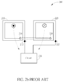
- FIG. 2b is a another simplified diagram of the conventional spiral inductor structure 200.
- the conventional spiral inductor structure 200 when the conventional spiral inductor structure 200 is coupled to the circuit 230 in another way, the first electromagnetic field generated by the first spiral inductor 210 and the second electromagnetic field generated by the second spiral inductor 220 are balance (i.e. equal) for the circuit 230.
- the conventional spiral inductor structure 200 still has a long and imbalance inter-connection since the inter-connection of the first spiral inductor 210 and the second spiral inductor 220 is connected between the second end point 214 and the fourth end point 224.
- the conventional spiral inductor structure 200 when the conventional spiral inductor structure 200 is coupled to a circuit 230 in this way, the first spiral inductor 210 and the second spiral inductor 220 have an unequal and imbalance lead length.
- the present invention aims at providing a composite inductor structure having lower parasitic coupling and well exploited mutual coupling in a smaller area, and a shorter and balance inter-connection, and an equal and balance lead length.
- one claimed composite inductor structure includes: a first spiral inductor and a second spiral inductor.
- the first spiral inductor has a plurality of loops and generates a first electromagnetic field, wherein an outermost loop of the first spiral inductor has a first end point, and an innermost loop of the first spiral inductor has a second end point.
- the second spiral inductor is arranged to be adjacent to the first spiral inductor, and has a plurality of loops and generates a second electromagnetic field, wherein an outermost loop of the second spiral inductor has a third end point, and an innermost loop of the second spiral inductor has a fourth end point, and the second spiral inductor is rotated by a specific degree with respect to an orientation of the first spiral inductor, and the first electromagnetic field and the second electromagnetic field are oppositely directed.
- FIG. 3 is a simplified diagram of a composite inductor structure 300 in accordance with a first embodiment of the present invention, wherein the composite inductor structure 300 can be applied to an integrated circuit (IC).
- the composite inductor structure 300 comprises: a first spiral inductor 310 and a second spiral inductor 320, wherein the first spiral inductor 310 and the second spiral inductor 320 are disposed on a same layer.
- the first spiral inductor 310 has two loops and generates a first electromagnetic field, wherein mutual coupling between the loops of the first spiral inductor 310 is well exploited in a smaller area in comparison with the prior art shown in FIG.
- the second spiral inductor 320 is arranged to be adjacent to the first spiral inductor 310, and has two loops and generates a second electromagnetic field, wherein mutual coupling between the loops of the second spiral inductor 320 is also well exploited in a smaller area in comparison with the prior art shown in FIG. 1 , and an outermost loop of the second spiral inductor 320 has a third end point 322, and an innermost loop of the second spiral inductor 320 has a fourth end point 324.
- the second spiral inductor 320 is rotated by 90 degree with respect to an orientation of the first spiral inductor 310, and the first electromagnetic field and the second electromagnetic field are oppositely directed.
- the first spiral inductor 310 and the second spiral inductor 320 are the same spiral inductors if second spiral inductor 320 is rotated by 0 degree or 360 degree with respect to an orientation of the first spiral inductor 310.
- the first spiral inductor 310 and the second spiral inductor 320 have an equal and balance lead length when the first spiral inductor 310 and the second spiral inductor 320 are coupled to a circuit 330, wherein the first end point 312 of the first spiral inductor 310 and the third end point 322 of the second spiral inductor 320 are coupled to the circuit 330.
- the first electromagnetic field and the second electromagnetic field are equal and opposite magnetic fields for the circuit 300, and thus the composite inductor structure 300 has a lower parasitic coupling to the circuit 330 (i.e. other components) in comparison with the prior art shown in FIG. 1 .
- first spiral inductor 310 and the second spiral inductor 320 are connected between the second end point 314 and the fourth end point 324, and thus the composite inductor structure 300 has a shorter and balance inter-connection in comparison with the prior art shown in FIG. 2a and FIG. 2b .
- the above embodiment is only for an illustrative purpose and are not meant to be a limitation of the present invention.
- the number of loops of the first spiral inductor 310 and the second spiral inductor 320 can be changed according to different design requirements, or the second spiral inductor 320 can be rotated by 180 degree with respect to an orientation of the first spiral inductor 310 according to different design requirements.
- shape of the first spiral inductor 310 and the second spiral inductor 320 also can be changed (for example, circle or other polygon types) according to different design requirements.
- FIG. 4 is a simplified diagram of a composite inductor structure 400 in accordance with a second embodiment of the present invention, wherein the composite inductor structure 400 can be applied to an IC.
- the composite inductor structure 400 comprises: a first spiral inductor 410 and a second spiral inductor 420, wherein the first spiral inductor 410 and the second spiral inductor 420 are disposed on a same layer.
- the first spiral inductor 410 has three loops and generates a first electromagnetic field, wherein mutual coupling between the loops of the first spiral inductor 410 is well exploited in a smaller area in comparison with the prior art shown in FIG.
- the second spiral inductor 420 is arranged to be adjacent to the first spiral inductor 410, and has three loops and generates a second electromagnetic field, wherein mutual coupling between the loops of the second spiral inductor 420 is also well exploited in a smaller area in comparison with the prior art shown in FIG. 1 , and an outermost loop of the second spiral inductor 420 has a third end point 422, and an innermost loop of the second spiral inductor 420 has a fourth end point 424.
- the second spiral inductor 420 is rotated by 90 degree with respect to an orientation of the first spiral inductor 410, and the first electromagnetic field and the second electromagnetic field are oppositely directed.
- the first spiral inductor 410 and the second spiral inductor 420 are the same spiral inductors if second spiral inductor 420 is rotated by 0 degree or 360 degree with respect to an orientation of the first spiral inductor 410.
- the first spiral inductor 410 and the second spiral inductor 420 have an equal and balance lead length when the first spiral inductor 410 and the second spiral inductor 420 are coupled to a circuit 430, wherein the first end point 412 of the first spiral inductor 410 and the third end point 422 of the second spiral inductor 420 are coupled to the circuit 430.
- the first electromagnetic field and the second electromagnetic field are equal and opposite magnetic fields for the circuit 430, and thus the composite inductor structure 400 has a lower parasitic coupling to the circuit 430 (i.e. other components) in comparison with the prior art shown in FIG. 1 .
- the composite inductor structure 400 has a shorter and balance inter-connection in comparison with the prior art shown in FIG. 2a and FIG. 2b .
- the above embodiment is only for an illustrative purpose and are not meant to be a limitation of the present invention.
- the number of loops of the first spiral inductor 410 and the second spiral inductor 420 can be changed according to different design requirements, or the second spiral inductor 420 can be rotated by 180 degree with respect to an orientation of the first spiral inductor 410 according to different design requirements.
- the shape of the first spiral inductor 410 and the second spiral inductor 420 also can be changed (for example, circle or other polygon types) according to different design requirements.
- FIG. 5 is a simplified diagram of a composite inductor structure 500 in accordance with a third embodiment of the present invention, wherein the composite inductor structure 500 can be applied to an IC.
- the composite inductor structure 500 comprises: a first spiral inductor 510 and a second spiral inductor 520, wherein the first spiral inductor 510 and the second spiral inductor 520 are disposed on a same layer.
- the first spiral inductor 510 has three loops and generates a first electromagnetic field, wherein mutual coupling between the loops of the first spiral inductor 510 is well exploited in a smaller area in comparison with the prior art shown in FIG.
- the second spiral inductor 520 is arranged to be adjacent to the first spiral inductor 510, and has three loops and generates a second electromagnetic field, wherein mutual coupling between the loops of the second spiral inductor 520 is also well exploited in a smaller area in comparison with the prior art shown in FIG. 1 , and an outermost loop of the second spiral inductor 520 has a third end point 522, and an innermost loop of the second spiral inductor 520 has a fourth end point 524.
- the second spiral inductor 520 is rotated by 90 degree with respect to an orientation of the first spiral inductor 510, and the first electromagnetic field and the second electromagnetic field are oppositely directed.
- the first spiral inductor 510 and the second spiral inductor 520 are the same spiral inductors if second spiral inductor 520 is rotated by 0 degree or 560 degree with respect to an orientation of the first spiral inductor 510.
- the first spiral inductor 510 and the second spiral inductor 520 have an equal and balance lead length when the first spiral inductor 510 and the second spiral inductor 520 are coupled to a circuit 530, wherein the first end point 512 of the first spiral inductor 510 and the third end point 522 of the second spiral inductor 520 are coupled to the circuit 530.
- the first electromagnetic field and the second electromagnetic field are equal and opposite magnetic fields for the circuit 530, and thus the composite inductor structure 500 has a lower parasitic coupling to the circuit 530 (i.e. other components) in comparison with the prior art shown in FIG. 1 .
- the composite inductor structure 500 has a shorter and balance inter-connection in comparison with the prior art shown in FIG. 2a and FIG. 2b .
- the above embodiment is only for an illustrative purpose and are not meant to be a limitation of the present invention.
- the number of loops of the first spiral inductor 510 and the second spiral inductor 520 can be changed according to different design requirements, or the second spiral inductor 520 can be rotated by 180 degree with respect to an orientation of the first spiral inductor 510 according to different design requirements.
- the shape of the first spiral inductor 510 and the second spiral inductor 520 also can be changed (for example, circle or other polygon types) according to different design requirements.
- the composite inductor structure disclosed by the present invention has lower parasitic coupling and well exploited mutual coupling in a smaller area, and a shorter and balance inter-connection, and an equal and balance lead length.
- the invention can be summarized as a composite inductor structure which comprises: a first spiral inductor and a second spiral inductor.
- the first spiral inductor has a plurality of loops and generates a first electromagnetic field, wherein an outermost loop of the first spiral inductor has a first end point, and an innermost loop of the first spiral inductor has a second end point.
- the second spiral inductor is arranged to be adjacent to the first spiral inductor, and has a plurality of loops and generates a second electromagnetic field, wherein an outermost loop of the second spiral inductor has a third end point, and an innermost loop of the second spiral inductor has a fourth end point, and the second spiral inductor is rotated by a specific degree with respect to an orientation of the first spiral inductor, and the first electromagnetic field and the second electromagnetic field are oppositely directed. All combinations and sub-combinations of the above-described features also belong to the invention.
Landscapes
- Engineering & Computer Science (AREA)
- Power Engineering (AREA)
- Microelectronics & Electronic Packaging (AREA)
- Coils Or Transformers For Communication (AREA)
- Semiconductor Integrated Circuits (AREA)
Abstract
Description
- The present invention relates to a composite inductor structure according to the pre-characterizing clauses of
claim 1. - Please refer to
FIG. 1. FIG. 1 shows a simplified block diagram of a conventionaltwisted inductor structure 100, wherein the conventionaltwisted inductor structure 100 generates two opposite magnetic fields. As shown inFIG. 1 , the conventionaltwisted inductor structure 100 comprises: afirst inductor 110 and asecond inductor 120, wherein thefirst inductor 110 has afirst end point 112 and asecond end point 114, and thesecond inductor 120 has athird end point 122 and afourth end point 124. An inter-connection of thefirst inductor 110 and thesecond inductor 120 is connected between thesecond end point 114 and thefourth end point 124, and the conventionaltwisted inductor structure 100 has a short inter-connection. However, thefirst inductor 110 has weak magnetic coupling with thesecond inductor 120, and the conventionaltwisted inductor structure 100 usually needs a large area since its mutual coupling is not well exploited. In addition, when the conventionaltwisted inductor structure 100 is coupled to acircuit 130, the electromagnetic fields generated by the conventionaltwisted inductor structure 100 are imbalance (i.e. not equal) for the circuit 130 (i.e. other components). - Please refer to
FIG. 2a. FIG. 2a is a simplified diagram of a conventionalspiral inductor structure 200. As shown inFIG. 2a , the conventionalspiral inductor structure 200 comprises: a firstspiral inductor 210 and a secondspiral inductor 220, wherein the firstspiral inductor 210 and the secondspiral inductor 220 are disposed on a same layer. The firstspiral inductor 210 has two loops and generates a first electromagnetic field, wherein mutual coupling between the loops of the firstspiral inductor 210 is well exploited in a smaller area in comparison with the prior art shown inFIG. 1 , and an outermost loop of the firstspiral inductor 210 has afirst end point 212, and an innermost loop of the firstspiral inductor 210 has asecond end point 214. The secondspiral inductor 220 is identical to the firstspiral inductor 210, and is arranged to be adjacent to the firstspiral inductor 210, and two loops and generates a second electromagnetic field, wherein mutual coupling between the loops of the secondspiral inductor 220 is also well exploited in a smaller area in comparison with the prior art shown inFIG. 1 , and an outermost loop of the secondspiral inductor 220 has athird end point 222, and an innermost loop of the secondspiral inductor 220 has afourth end point 224. However, the conventionalspiral inductor structure 200 has a long and imbalance inter-connection since the inter-connection of the firstspiral inductor 210 and the secondspiral inductor 220 is connected between thesecond end point 214 and thefourth end point 224. In addition, when the conventionalspiral inductor structure 200 is coupled to acircuit 230, the first electromagnetic field generated by the firstspiral inductor 210 and the second electromagnetic field generated by the secondspiral inductor 220 are imbalance (i.e. not equal) for the circuit 230 (i.e. other components). - Please refer to
FIG. 2b. FIG. 2b is a another simplified diagram of the conventionalspiral inductor structure 200. As shown inFIG. 2b , when the conventionalspiral inductor structure 200 is coupled to thecircuit 230 in another way, the first electromagnetic field generated by the firstspiral inductor 210 and the second electromagnetic field generated by the secondspiral inductor 220 are balance (i.e. equal) for thecircuit 230. However, the conventionalspiral inductor structure 200 still has a long and imbalance inter-connection since the inter-connection of the firstspiral inductor 210 and the secondspiral inductor 220 is connected between thesecond end point 214 and thefourth end point 224. In addition, when the conventionalspiral inductor structure 200 is coupled to acircuit 230 in this way, the firstspiral inductor 210 and the secondspiral inductor 220 have an unequal and imbalance lead length. - This in mind, the present invention aims at providing a composite inductor structure having lower parasitic coupling and well exploited mutual coupling in a smaller area, and a shorter and balance inter-connection, and an equal and balance lead length.
- This is achieved by a composite inductor structure according to the
independent claim 1. The respective dependent claims pertain to corresponding further developments and improvements. - As will be seen more clearly from the detailed description following below, one claimed composite inductor structure includes: a first spiral inductor and a second spiral inductor. The first spiral inductor has a plurality of loops and generates a first electromagnetic field, wherein an outermost loop of the first spiral inductor has a first end point, and an innermost loop of the first spiral inductor has a second end point. The second spiral inductor is arranged to be adjacent to the first spiral inductor, and has a plurality of loops and generates a second electromagnetic field, wherein an outermost loop of the second spiral inductor has a third end point, and an innermost loop of the second spiral inductor has a fourth end point, and the second spiral inductor is rotated by a specific degree with respect to an orientation of the first spiral inductor, and the first electromagnetic field and the second electromagnetic field are oppositely directed.
- In the following, the invention is further illustrated by way of example, taking reference to the accompanying drawings. Thereof
-
FIG. 1 shows a simplified block diagram of a conventional twisted inductor structure. -
FIG. 2a is a simplified diagram of a conventional spiral inductor structure. -
FIG. 2b is a another simplified diagram of the conventional spiral inductor structure. -
FIG. 3 is a simplified diagram of a composite inductor structure in accordance with a first embodiment of the present invention. -
FIG. 4 is a simplified diagram of a composite inductor structure in accordance with a second embodiment of the present invention. -
FIG. 5 is a simplified diagram of a composite inductor structure in accordance with a third embodiment of the present invention. - Certain terms are used throughout the description and following claims to refer to particular components. As one skilled in the art will appreciate, manufacturers may refer to a component by different names. This document does not intend point to distinguish between components that differ in name but not function. In the following description and in the claims, the terms "include" and "comprise" are used in an open-end pointed fashion, and thus should be interpreted to mean "include, but not limited to". Also, the term "couple" is intend pointed to mean either an indirect or direct electrical connection. Accordingly, if one device is coupled to another device, that connection may be through a direct electrical connection, or through an indirect electrical connection via other devices and connections.
- Please refer to
FIG. 3. FIG. 3 is a simplified diagram of acomposite inductor structure 300 in accordance with a first embodiment of the present invention, wherein thecomposite inductor structure 300 can be applied to an integrated circuit (IC). As shown inFIG. 3 , thecomposite inductor structure 300 comprises: a firstspiral inductor 310 and a secondspiral inductor 320, wherein the firstspiral inductor 310 and the secondspiral inductor 320 are disposed on a same layer. The firstspiral inductor 310 has two loops and generates a first electromagnetic field, wherein mutual coupling between the loops of the firstspiral inductor 310 is well exploited in a smaller area in comparison with the prior art shown inFIG. 1 , and an outermost loop of the firstspiral inductor 310 has afirst end point 312, and an innermost loop of the firstspiral inductor 310 has asecond end point 314. The secondspiral inductor 320 is arranged to be adjacent to the firstspiral inductor 310, and has two loops and generates a second electromagnetic field, wherein mutual coupling between the loops of the secondspiral inductor 320 is also well exploited in a smaller area in comparison with the prior art shown inFIG. 1 , and an outermost loop of the secondspiral inductor 320 has athird end point 322, and an innermost loop of the secondspiral inductor 320 has afourth end point 324. The secondspiral inductor 320 is rotated by 90 degree with respect to an orientation of the firstspiral inductor 310, and the first electromagnetic field and the second electromagnetic field are oppositely directed. In addition, the firstspiral inductor 310 and the secondspiral inductor 320 are the same spiral inductors if secondspiral inductor 320 is rotated by 0 degree or 360 degree with respect to an orientation of the firstspiral inductor 310. - The first
spiral inductor 310 and the secondspiral inductor 320 have an equal and balance lead length when the firstspiral inductor 310 and the secondspiral inductor 320 are coupled to acircuit 330, wherein thefirst end point 312 of the firstspiral inductor 310 and thethird end point 322 of the secondspiral inductor 320 are coupled to thecircuit 330. The first electromagnetic field and the second electromagnetic field are equal and opposite magnetic fields for thecircuit 300, and thus thecomposite inductor structure 300 has a lower parasitic coupling to the circuit 330 (i.e. other components) in comparison with the prior art shown inFIG. 1 . In addition, an inter-connection of the firstspiral inductor 310 and the secondspiral inductor 320 is connected between thesecond end point 314 and thefourth end point 324, and thus thecomposite inductor structure 300 has a shorter and balance inter-connection in comparison with the prior art shown inFIG. 2a andFIG. 2b . Please note that the above embodiment is only for an illustrative purpose and are not meant to be a limitation of the present invention. For example, the number of loops of the firstspiral inductor 310 and the secondspiral inductor 320 can be changed according to different design requirements, or the secondspiral inductor 320 can be rotated by 180 degree with respect to an orientation of the firstspiral inductor 310 according to different design requirements. In addition, the shape of the firstspiral inductor 310 and the secondspiral inductor 320 also can be changed (for example, circle or other polygon types) according to different design requirements. - Please refer to
FIG. 4. FIG. 4 is a simplified diagram of acomposite inductor structure 400 in accordance with a second embodiment of the present invention, wherein thecomposite inductor structure 400 can be applied to an IC. As shown inFIG. 4 , thecomposite inductor structure 400 comprises: a firstspiral inductor 410 and a secondspiral inductor 420, wherein the firstspiral inductor 410 and the secondspiral inductor 420 are disposed on a same layer. Thefirst spiral inductor 410 has three loops and generates a first electromagnetic field, wherein mutual coupling between the loops of thefirst spiral inductor 410 is well exploited in a smaller area in comparison with the prior art shown inFIG. 1 , and an outermost loop of thefirst spiral inductor 410 has afirst end point 412, and an innermost loop of thefirst spiral inductor 410 has asecond end point 414. Thesecond spiral inductor 420 is arranged to be adjacent to thefirst spiral inductor 410, and has three loops and generates a second electromagnetic field, wherein mutual coupling between the loops of thesecond spiral inductor 420 is also well exploited in a smaller area in comparison with the prior art shown inFIG. 1 , and an outermost loop of thesecond spiral inductor 420 has athird end point 422, and an innermost loop of thesecond spiral inductor 420 has afourth end point 424. Thesecond spiral inductor 420 is rotated by 90 degree with respect to an orientation of thefirst spiral inductor 410, and the first electromagnetic field and the second electromagnetic field are oppositely directed. In addition, thefirst spiral inductor 410 and thesecond spiral inductor 420 are the same spiral inductors ifsecond spiral inductor 420 is rotated by 0 degree or 360 degree with respect to an orientation of thefirst spiral inductor 410. - The
first spiral inductor 410 and thesecond spiral inductor 420 have an equal and balance lead length when thefirst spiral inductor 410 and thesecond spiral inductor 420 are coupled to acircuit 430, wherein thefirst end point 412 of thefirst spiral inductor 410 and thethird end point 422 of thesecond spiral inductor 420 are coupled to thecircuit 430. The first electromagnetic field and the second electromagnetic field are equal and opposite magnetic fields for thecircuit 430, and thus thecomposite inductor structure 400 has a lower parasitic coupling to the circuit 430 (i.e. other components) in comparison with the prior art shown inFIG. 1 . In addition, thesecond end point 414 is coupled to a first supply rail and thefourth end point 424 is coupled to a second supply rail, and thus thecomposite inductor structure 400 has a shorter and balance inter-connection in comparison with the prior art shown inFIG. 2a andFIG. 2b . Please note that the above embodiment is only for an illustrative purpose and are not meant to be a limitation of the present invention. For example, the number of loops of thefirst spiral inductor 410 and thesecond spiral inductor 420 can be changed according to different design requirements, or thesecond spiral inductor 420 can be rotated by 180 degree with respect to an orientation of thefirst spiral inductor 410 according to different design requirements. In addition, the shape of thefirst spiral inductor 410 and thesecond spiral inductor 420 also can be changed (for example, circle or other polygon types) according to different design requirements. - Please refer to
FIG. 5. FIG. 5 is a simplified diagram of acomposite inductor structure 500 in accordance with a third embodiment of the present invention, wherein thecomposite inductor structure 500 can be applied to an IC. As shown inFIG. 5 , thecomposite inductor structure 500 comprises: afirst spiral inductor 510 and asecond spiral inductor 520, wherein thefirst spiral inductor 510 and thesecond spiral inductor 520 are disposed on a same layer. Thefirst spiral inductor 510 has three loops and generates a first electromagnetic field, wherein mutual coupling between the loops of thefirst spiral inductor 510 is well exploited in a smaller area in comparison with the prior art shown inFIG. 1 , and an outermost loop of thefirst spiral inductor 510 has afirst end point 512, and an innermost loop of thefirst spiral inductor 510 has asecond end point 514. Thesecond spiral inductor 520 is arranged to be adjacent to thefirst spiral inductor 510, and has three loops and generates a second electromagnetic field, wherein mutual coupling between the loops of thesecond spiral inductor 520 is also well exploited in a smaller area in comparison with the prior art shown inFIG. 1 , and an outermost loop of thesecond spiral inductor 520 has athird end point 522, and an innermost loop of thesecond spiral inductor 520 has afourth end point 524. Thesecond spiral inductor 520 is rotated by 90 degree with respect to an orientation of thefirst spiral inductor 510, and the first electromagnetic field and the second electromagnetic field are oppositely directed. In addition, thefirst spiral inductor 510 and thesecond spiral inductor 520 are the same spiral inductors ifsecond spiral inductor 520 is rotated by 0 degree or 560 degree with respect to an orientation of thefirst spiral inductor 510. - The
first spiral inductor 510 and thesecond spiral inductor 520 have an equal and balance lead length when thefirst spiral inductor 510 and thesecond spiral inductor 520 are coupled to acircuit 530, wherein thefirst end point 512 of thefirst spiral inductor 510 and thethird end point 522 of thesecond spiral inductor 520 are coupled to thecircuit 530. The first electromagnetic field and the second electromagnetic field are equal and opposite magnetic fields for thecircuit 530, and thus thecomposite inductor structure 500 has a lower parasitic coupling to the circuit 530 (i.e. other components) in comparison with the prior art shown inFIG. 1 . In addition, thesecond end point 514 and thefourth end point 524 are coupled to a supply rail, and thus thecomposite inductor structure 500 has a shorter and balance inter-connection in comparison with the prior art shown inFIG. 2a andFIG. 2b . Please note that the above embodiment is only for an illustrative purpose and are not meant to be a limitation of the present invention. For example, the number of loops of thefirst spiral inductor 510 and thesecond spiral inductor 520 can be changed according to different design requirements, or thesecond spiral inductor 520 can be rotated by 180 degree with respect to an orientation of thefirst spiral inductor 510 according to different design requirements. In addition, the shape of thefirst spiral inductor 510 and thesecond spiral inductor 520 also can be changed (for example, circle or other polygon types) according to different design requirements. - Briefly summarized, the composite inductor structure disclosed by the present invention has lower parasitic coupling and well exploited mutual coupling in a smaller area, and a shorter and balance inter-connection, and an equal and balance lead length.
- The invention can be summarized as a composite inductor structure which comprises: a first spiral inductor and a second spiral inductor. The first spiral inductor has a plurality of loops and generates a first electromagnetic field, wherein an outermost loop of the first spiral inductor has a first end point, and an innermost loop of the first spiral inductor has a second end point. The second spiral inductor is arranged to be adjacent to the first spiral inductor, and has a plurality of loops and generates a second electromagnetic field, wherein an outermost loop of the second spiral inductor has a third end point, and an innermost loop of the second spiral inductor has a fourth end point, and the second spiral inductor is rotated by a specific degree with respect to an orientation of the first spiral inductor, and the first electromagnetic field and the second electromagnetic field are oppositely directed. All combinations and sub-combinations of the above-described features also belong to the invention.
Claims (9)
- A composite inductor structure (300, 400, 500), comprising:a first spiral inductor (310, 410, 510), having a plurality of loops and generating a first electromagnetic field, wherein an outermost loop of the first spiral inductor (310, 410, 510) has a first end point (312, 412, 512), and an innermost loop of the first spiral inductor (310, 410, 510) has a second end point (314, 414, 514); anda second spiral inductor (320, 420, 520), arranged to be adjacent to the first spiral inductor (310, 410, 510), having a plurality of loops and generating a second electromagnetic field, wherein an outermost loop of the second spiral inductor (320, 420, 520) has a third end point (322, 422, 522), and an innermost loop of the second spiral inductor (320, 420, 520) has a fourth end point (324, 424, 524), and the second spiral inductor (320, 420, 520) is rotated by a specific degree with respect to an orientation of the first spiral inductor (310, 410, 510), and the first electromagnetic field and the second electromagnetic field are oppositely directed.
- The composite inductor structure (300, 400, 500) of claim 1, wherein the specific degree is 90 degree.
- The composite inductor structure (300, 400, 500) of claim 1, wherein the first spiral inductor (310, 410, 510) and the second spiral inductor (320, 420, 520) have an equal and balance lead length when the first spiral inductor (310, 410, 510) and the second spiral inductor (320, 420, 520) are coupled to a circuit (330, 430, 530).
- The composite inductor structure (300, 400, 500) of claim 3, wherein the first end point (312, 412, 512) and the third end point (322, 422, 522) are coupled to the circuit (330, 430, 530).
- The composite inductor structure (300, 400, 500) of claim 3, wherein the first electromagnetic field and the second electromagnetic field are equal and opposite magnetic fields for the circuit (330, 430, 530).
- The composite inductor structure (300, 400, 500) of claim 1, wherein an inter-connection of the first spiral inductor (310, 410, 510) and the second spiral inductor (320, 420, 520) is connected between the second end point (314, 414, 514) and the fourth end point (324, 424, 524).
- The composite inductor structure (400) of claim 1, wherein the second end point (414) is coupled to a first supply rail and the fourth end point (424) is coupled to a second supply rail.
- The composite inductor structure (500) of claim 1, wherein the second end point (514) and the fourth end point (524) are coupled to a supply rail.
- The composite inductor structure (300, 400, 500) of claim 1, applied to an integrated circuit (IC)
Applications Claiming Priority (2)
| Application Number | Priority Date | Filing Date | Title |
|---|---|---|---|
| US201662297998P | 2016-02-22 | 2016-02-22 | |
| US15/186,554 US20170243690A1 (en) | 2016-02-22 | 2016-06-20 | Composite inductor structure |
Publications (1)
| Publication Number | Publication Date |
|---|---|
| EP3208813A1 true EP3208813A1 (en) | 2017-08-23 |
Family
ID=56567412
Family Applications (1)
| Application Number | Title | Priority Date | Filing Date |
|---|---|---|---|
| EP16181032.0A Withdrawn EP3208813A1 (en) | 2016-02-22 | 2016-07-25 | Composite inductor structure |
Country Status (4)
| Country | Link |
|---|---|
| US (1) | US20170243690A1 (en) |
| EP (1) | EP3208813A1 (en) |
| CN (1) | CN107103990A (en) |
| TW (1) | TW201730904A (en) |
Families Citing this family (2)
| Publication number | Priority date | Publication date | Assignee | Title |
|---|---|---|---|---|
| US10453705B2 (en) * | 2018-01-09 | 2019-10-22 | Intel Corporation | Multi-voltage apparatus for electronics package including magnetic inductor and capacitor and manufacturing thereof |
| EP3839991B1 (en) * | 2019-12-20 | 2024-06-12 | Socionext Inc. | Integrated circuitry comprising inductor arrangements |
Citations (5)
| Publication number | Priority date | Publication date | Assignee | Title |
|---|---|---|---|---|
| JPH0382106A (en) * | 1989-08-25 | 1991-04-08 | Fujitsu Ltd | Flat coil |
| US6236297B1 (en) * | 1998-07-08 | 2001-05-22 | Winbond Electronics Corp. | Combinational inductor |
| US20050195061A1 (en) * | 2004-03-03 | 2005-09-08 | Atheros Communications, Inc. | Inductor layout using step symmetry for inductors |
| US20090244866A1 (en) * | 2008-03-07 | 2009-10-01 | Nec Electronics Corporation | Circuit Device |
| US20150206634A1 (en) * | 2014-01-17 | 2015-07-23 | Marvell World Trade Ltd | Pseudo-8-shaped inductor |
Family Cites Families (5)
| Publication number | Priority date | Publication date | Assignee | Title |
|---|---|---|---|---|
| JP2955124B2 (en) * | 1992-05-25 | 1999-10-04 | 松下電器産業株式会社 | Answering machine for ISDN and answering machine for ISDN |
| JP2005327931A (en) * | 2004-05-14 | 2005-11-24 | Sony Corp | Integrated inductor and receiving circuit using the same |
| TWI360254B (en) * | 2008-09-10 | 2012-03-11 | Advanced Semiconductor Eng | Balun circuit manufactured by integrate passive de |
| TWM411649U (en) * | 2011-01-17 | 2011-09-11 | Yujing Technology Co Ltd | Building-block combined-type high-power transformer |
| JP6030107B2 (en) * | 2014-11-28 | 2016-11-24 | ルネサスエレクトロニクス株式会社 | Circuit equipment |
-
2016
- 2016-06-20 US US15/186,554 patent/US20170243690A1/en not_active Abandoned
- 2016-07-25 EP EP16181032.0A patent/EP3208813A1/en not_active Withdrawn
-
2017
- 2017-02-14 CN CN201710078032.7A patent/CN107103990A/en active Pending
- 2017-02-21 TW TW106105736A patent/TW201730904A/en unknown
Patent Citations (5)
| Publication number | Priority date | Publication date | Assignee | Title |
|---|---|---|---|---|
| JPH0382106A (en) * | 1989-08-25 | 1991-04-08 | Fujitsu Ltd | Flat coil |
| US6236297B1 (en) * | 1998-07-08 | 2001-05-22 | Winbond Electronics Corp. | Combinational inductor |
| US20050195061A1 (en) * | 2004-03-03 | 2005-09-08 | Atheros Communications, Inc. | Inductor layout using step symmetry for inductors |
| US20090244866A1 (en) * | 2008-03-07 | 2009-10-01 | Nec Electronics Corporation | Circuit Device |
| US20150206634A1 (en) * | 2014-01-17 | 2015-07-23 | Marvell World Trade Ltd | Pseudo-8-shaped inductor |
Also Published As
| Publication number | Publication date |
|---|---|
| TW201730904A (en) | 2017-09-01 |
| CN107103990A (en) | 2017-08-29 |
| US20170243690A1 (en) | 2017-08-24 |
Similar Documents
| Publication | Publication Date | Title |
|---|---|---|
| US9941744B2 (en) | Non-contact power supply circuit | |
| JP7598421B2 (en) | Power transmission system and control method | |
| US10748701B2 (en) | Inductor device | |
| TWI344805B (en) | Inductor and electric power supply using it | |
| US11437910B2 (en) | Power module | |
| CN105024459B (en) | Wireless power reception device and the electronic device for including the wireless power reception device | |
| US11676884B2 (en) | Cantilevered leadframe support structure for magnetic wireless transfer between integrated circuit dies | |
| US10484050B2 (en) | Near field communication ring | |
| CN108511174A (en) | A kind of coil module, radio energy radiating circuit and receiving circuit | |
| CN1672223A (en) | Planar inductance | |
| EP2824678A1 (en) | Power supply device, power reception device, and power supply/reception device | |
| JPWO2015137431A1 (en) | Power receiving coil structure and wireless power feeding system | |
| CN107666188A (en) | Electric power capture for RFID/NFC applications | |
| EP2670035A1 (en) | Dc-dc convertor module and multilayer substrate | |
| CN101197507A (en) | Wireless power device and circuit | |
| CN103780098B (en) | Output voltage feedback circuit, isolated converter and integrated circuit used therein | |
| CN108462261B (en) | Coil module, electric energy transmitting circuit and electric energy receiving circuit | |
| CN105304606B (en) | Electronic device with two-plane type inductor | |
| KR102029491B1 (en) | Coil component and and board for mounting the same | |
| US20170243690A1 (en) | Composite inductor structure | |
| CN107077950B (en) | Embedded thin film magnetic carrier for integrated voltage regulator | |
| JP6315109B2 (en) | Power supply device | |
| US11783991B2 (en) | Inductor device | |
| CN113196473A (en) | Integrated component and power conversion device | |
| JP4573498B2 (en) | Ultra-compact power converter |
Legal Events
| Date | Code | Title | Description |
|---|---|---|---|
| PUAI | Public reference made under article 153(3) epc to a published international application that has entered the european phase |
Free format text: ORIGINAL CODE: 0009012 |
|
| AK | Designated contracting states |
Kind code of ref document: A1 Designated state(s): AL AT BE BG CH CY CZ DE DK EE ES FI FR GB GR HR HU IE IS IT LI LT LU LV MC MK MT NL NO PL PT RO RS SE SI SK SM TR |
|
| AX | Request for extension of the european patent |
Extension state: BA ME |
|
| 17P | Request for examination filed |
Effective date: 20171117 |
|
| RBV | Designated contracting states (corrected) |
Designated state(s): AL AT BE BG CH CY CZ DE DK EE ES FI FR GB GR HR HU IE IS IT LI LT LU LV MC MK MT NL NO PL PT RO RS SE SI SK SM TR |
|
| 17Q | First examination report despatched |
Effective date: 20181031 |
|
| STAA | Information on the status of an ep patent application or granted ep patent |
Free format text: STATUS: THE APPLICATION HAS BEEN WITHDRAWN |
|
| 18W | Application withdrawn |
Effective date: 20190130 |