EP3206113A1 - Touch screen and terminal - Google Patents
Touch screen and terminal Download PDFInfo
- Publication number
- EP3206113A1 EP3206113A1 EP15849222.3A EP15849222A EP3206113A1 EP 3206113 A1 EP3206113 A1 EP 3206113A1 EP 15849222 A EP15849222 A EP 15849222A EP 3206113 A1 EP3206113 A1 EP 3206113A1
- Authority
- EP
- European Patent Office
- Prior art keywords
- touch screen
- antenna
- terminal
- conducting layer
- touch
- Prior art date
- Legal status (The legal status is an assumption and is not a legal conclusion. Google has not performed a legal analysis and makes no representation as to the accuracy of the status listed.)
- Ceased
Links
Images


Classifications
-
- H—ELECTRICITY
- H05—ELECTRIC TECHNIQUES NOT OTHERWISE PROVIDED FOR
- H05K—PRINTED CIRCUITS; CASINGS OR CONSTRUCTIONAL DETAILS OF ELECTRIC APPARATUS; MANUFACTURE OF ASSEMBLAGES OF ELECTRICAL COMPONENTS
- H05K1/00—Printed circuits
- H05K1/18—Printed circuits structurally associated with non-printed electric components
- H05K1/189—Printed circuits structurally associated with non-printed electric components characterised by the use of a flexible or folded printed circuit
-
- G—PHYSICS
- G06—COMPUTING; CALCULATING OR COUNTING
- G06F—ELECTRIC DIGITAL DATA PROCESSING
- G06F3/00—Input arrangements for transferring data to be processed into a form capable of being handled by the computer; Output arrangements for transferring data from processing unit to output unit, e.g. interface arrangements
- G06F3/01—Input arrangements or combined input and output arrangements for interaction between user and computer
- G06F3/03—Arrangements for converting the position or the displacement of a member into a coded form
- G06F3/041—Digitisers, e.g. for touch screens or touch pads, characterised by the transducing means
- G06F3/0412—Digitisers structurally integrated in a display
-
- H—ELECTRICITY
- H01—ELECTRIC ELEMENTS
- H01Q—ANTENNAS, i.e. RADIO AERIALS
- H01Q1/00—Details of, or arrangements associated with, antennas
- H01Q1/12—Supports; Mounting means
- H01Q1/22—Supports; Mounting means by structural association with other equipment or articles
- H01Q1/24—Supports; Mounting means by structural association with other equipment or articles with receiving set
- H01Q1/241—Supports; Mounting means by structural association with other equipment or articles with receiving set used in mobile communications, e.g. GSM
- H01Q1/242—Supports; Mounting means by structural association with other equipment or articles with receiving set used in mobile communications, e.g. GSM specially adapted for hand-held use
- H01Q1/243—Supports; Mounting means by structural association with other equipment or articles with receiving set used in mobile communications, e.g. GSM specially adapted for hand-held use with built-in antennas
-
- H—ELECTRICITY
- H01—ELECTRIC ELEMENTS
- H01Q—ANTENNAS, i.e. RADIO AERIALS
- H01Q1/00—Details of, or arrangements associated with, antennas
- H01Q1/36—Structural form of radiating elements, e.g. cone, spiral, umbrella; Particular materials used therewith
- H01Q1/38—Structural form of radiating elements, e.g. cone, spiral, umbrella; Particular materials used therewith formed by a conductive layer on an insulating support
-
- H—ELECTRICITY
- H05—ELECTRIC TECHNIQUES NOT OTHERWISE PROVIDED FOR
- H05K—PRINTED CIRCUITS; CASINGS OR CONSTRUCTIONAL DETAILS OF ELECTRIC APPARATUS; MANUFACTURE OF ASSEMBLAGES OF ELECTRICAL COMPONENTS
- H05K1/00—Printed circuits
- H05K1/02—Details
- H05K1/0277—Bendability or stretchability details
- H05K1/028—Bending or folding regions of flexible printed circuits
-
- G—PHYSICS
- G06—COMPUTING; CALCULATING OR COUNTING
- G06F—ELECTRIC DIGITAL DATA PROCESSING
- G06F2203/00—Indexing scheme relating to G06F3/00 - G06F3/048
- G06F2203/041—Indexing scheme relating to G06F3/041 - G06F3/045
- G06F2203/04102—Flexible digitiser, i.e. constructional details for allowing the whole digitising part of a device to be flexed or rolled like a sheet of paper
-
- H—ELECTRICITY
- H05—ELECTRIC TECHNIQUES NOT OTHERWISE PROVIDED FOR
- H05K—PRINTED CIRCUITS; CASINGS OR CONSTRUCTIONAL DETAILS OF ELECTRIC APPARATUS; MANUFACTURE OF ASSEMBLAGES OF ELECTRICAL COMPONENTS
- H05K1/00—Printed circuits
- H05K1/02—Details
- H05K1/0213—Electrical arrangements not otherwise provided for
- H05K1/0237—High frequency adaptations
-
- H—ELECTRICITY
- H05—ELECTRIC TECHNIQUES NOT OTHERWISE PROVIDED FOR
- H05K—PRINTED CIRCUITS; CASINGS OR CONSTRUCTIONAL DETAILS OF ELECTRIC APPARATUS; MANUFACTURE OF ASSEMBLAGES OF ELECTRICAL COMPONENTS
- H05K2201/00—Indexing scheme relating to printed circuits covered by H05K1/00
- H05K2201/10—Details of components or other objects attached to or integrated in a printed circuit board
- H05K2201/10007—Types of components
- H05K2201/10098—Components for radio transmission, e.g. radio frequency identification [RFID] tag, printed or non-printed antennas
Definitions
- the disclosure relates to the technical field of communications, and more particularly to a touch screen and a terminal.
- a conventional antenna is attached to a shell as a Flexible Printed Circuit (FPC) or sheet steel, and then is connected with a main board through a leaf spring or a PIN to form a circuit, which is required to reserve an enough area for the antenna in a structure of the shell.
- FPC Flexible Printed Circuit
- mobile terminals are developed to be light, thin and large, and spaces for antennae are compressed to be smaller and smaller, so it is more and more difficult to design antennae.
- designing of the antenna needs to avoid the metal component, or utilize the metal component to make the metal component form a part of the antenna.
- Such a design method limits an appearance design of the terminal, or forms a similar uncreative design. Aesthetic appearance and practicability may not be achieved at the same time.
- the disclosure provides a touch screen and terminal, which are adopted to solve the problem that the conventional arrangement manner for an antenna restricts the appearance and material designing for a terminal in the related art.
- a touch screen includes: a touch layer, a conducting layer and a substrate layer which are laminated and matched in sequence, wherein an antenna radiating body, and an antenna signal line and a ground feeder line which are connected with the antenna radiating body are arranged on the conducting layer.
- the antenna radiating body, the antenna signal line and the ground feeder line are arranged in a non-display area on the conducting layer, or are arranged in a non-touch area in a display area on the conducting layer.
- the antenna signal line and the ground feeder line are led out through an FPC to be connected with a radio frequency chip.
- a baseband control line configured to respond to a touch signal is further arranged on the conducting layer, and the baseband control line is led out through the FPC to be connected with a baseband processing chip.
- the antenna radiating body arranged on the conducting layer is formed by adopting a spraying and coating manner, an electroplating manner or an implementable process for forming a conducting film of the touch screen.
- a terminal includes the abovementioned touch screen.
- the antenna signal line and the ground feeder line which are arranged on the conducting layer of the touch screen are led out of the touch screen through an FPC to be connected to a radio frequency chip on a main board of the terminal.
- a baseband control line arranged on the conducting layer of the touch screen is led out through the FPC to be connected to a baseband processing chip on the main board of the terminal.
- the antenna radiating body is arranged on the touch screen to implement the arrangement for an antenna.
- Such an arrangement manner can achieve better antenna radiating performance, and can also have no limitation on the appearance design of the terminal; such an arrangement manner reduces the thickness of the terminal, influences that the metal component affects the antenna and assembling procedures of the antenna; and improves consistency for assembling the antenna.
- the embodiments of the disclosure provide a touch screen and a terminal. Wires are arranged on a conducting layer of the touch screen to realize a function of the antenna, so that the terminal with the touch screen can achieve better antenna radiating performance, and can also have no limitation on the appearance design of the terminal.
- the embodiment of the disclosure provides a touch screen.
- the touch screen includes a touch layer 6, a conducting layer 7 and substrate layer 8, which are laminated and matched in sequence.
- an antenna radiating body, and an antenna signal line and a ground feeder line which are connected with the antenna radiating body are arranged on the conducting layer 7, wherein when the antenna radiating body, and the antenna signal line and the ground feeder line which are connected with the antenna radiating body are arranged, a basic arrangement principle is that a baseband control line (wiring configured to realize a touch function) of the touch screen is avoided. Therefore, in the embodiment of the disclosure, the antenna radiating body, the antenna signal line and the ground feeder line are arranged in a non-display area on the conducting layer.
- a touch screen on a mobile phone terminal is taken as an example, so the antenna radiating body, the antenna signal line and the ground feeder line may be arranged in a non-display area which is positioned above a display area of the mobile phone terminal, as shown in Fig. 2 , or the antenna radiating body, the antenna signal line and the ground feeder line may be arranged in a non-display area which is positioned below the display area of the mobile phone terminal, as shown in Fig. 3 .
- Fig. 4 is a simple bending diagram showing a touch screen.
- the touch screen may be bent in leftward, rightward, upward and downward directions, and in the figure, areas B, C, D and E are bent areas.
- bending the touch screen is based on different purposes, wherein there are some conditions where the bent areas are only configured for display and not respond to a touch operation.
- the antenna radiating body and antenna wiring may be arranged in a non-touch area in a display area of the conducting layer.
- the antenna signal line and the ground feeder line are led out through an FPC so as to be connected with a radio frequency chip, so an antenna radiating and receiving circuit is formed.
- a forming manner for the antenna radiating body arranged on the conducting layer includes, but not limited to: a spraying and coating manner, an electroplating manner or an implementable process for forming a conducting film of the touch screen.
- wiring is performed on the conducting layer of the touch screen to realize the function of the antenna, and supports are provided for the terminal to achieve better antenna radiating performance of the terminal and have no limitation on the appearance design of the terminal.
- the embodiment of the disclosure provides a terminal.
- the terminal includes the touch screen of embodiment 1, that is, the terminal of the embodiment improves a conventional antenna arrangement manner, and an antenna is arranged through the touch screen.
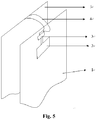
- 1 is a main board of the terminal; 2 is a radio frequency chip arranged on the main board; 3 is a connector arranged on the main board; 4 is an FPC of the touch screen; and 5 is the touch screen with the antenna.
- An antenna signal line and a ground feeder line which are arranged on a conducting layer in the touch screen 5 are connected with the radio frequency chip 2 on the main board 1 through the FPC 4 and the connector 3 so as to form a circuit.
- the FPC 4 may include a touch signal of the touch screen 5, and when the touch signal is included, after the connector 3 is connected with the main board 1, the signal line of the touch signal is connected with a baseband processing chip.
- the antenna signal line is connected with the radio frequency chip 2.
- the antenna radiating body is arranged on the touch screen of the terminal, so that an available space for the antenna is greatly utilized, and the thickness of the terminal and influences that the metal component affects the antenna are reduced. In addition, assembling procedures of the antenna are reduced, and the consistency for assembling the antenna is improved.
- the antenna radiating body is arranged on the touch screen to implement the arrangement for an antenna.
- Such an arrangement manner can achieve better antenna radiating performance, and can also have no limitation on the appearance design of the terminal; such an arrangement manner reduces the thickness of the terminal, influences that the metal component affects the antenna and assembling procedures of the antenna; and improves consistency for assembling the antenna.
Abstract
Description
- The disclosure relates to the technical field of communications, and more particularly to a touch screen and a terminal.
- A conventional antenna is attached to a shell as a Flexible Printed Circuit (FPC) or sheet steel, and then is connected with a main board through a leaf spring or a PIN to form a circuit, which is required to reserve an enough area for the antenna in a structure of the shell. However, mobile terminals are developed to be light, thin and large, and spaces for antennae are compressed to be smaller and smaller, so it is more and more difficult to design antennae. Particularly, when a metal component is arranged on a shell of a terminal, for achieving high radiation performance of an antenna, designing of the antenna needs to avoid the metal component, or utilize the metal component to make the metal component form a part of the antenna. Such a design method limits an appearance design of the terminal, or forms a similar uncreative design. Aesthetic appearance and practicability may not be achieved at the same time.
- The disclosure provides a touch screen and terminal, which are adopted to solve the problem that the conventional arrangement manner for an antenna restricts the appearance and material designing for a terminal in the related art.
- A touch screen includes: a touch layer, a conducting layer and a substrate layer which are laminated and matched in sequence, wherein an antenna radiating body, and an antenna signal line and a ground feeder line which are connected with the antenna radiating body are arranged on the conducting layer.
- Alternatively, in the touch screen of embodiments of the disclosure, the antenna radiating body, the antenna signal line and the ground feeder line are arranged in a non-display area on the conducting layer, or are arranged in a non-touch area in a display area on the conducting layer.
- Alternatively, in the touch screen of the embodiments of the disclosure, the antenna signal line and the ground feeder line are led out through an FPC to be connected with a radio frequency chip.
- Alternatively, in the touch screen of the embodiments of the disclosure, a baseband control line configured to respond to a touch signal is further arranged on the conducting layer, and the baseband control line is led out through the FPC to be connected with a baseband processing chip.
- Alternatively, in the touch screen of the embodiments of the disclosure, the antenna radiating body arranged on the conducting layer is formed by adopting a spraying and coating manner, an electroplating manner or an implementable process for forming a conducting film of the touch screen.
- A terminal includes the abovementioned touch screen.
- Alternatively, in the terminal of the embodiments of the disclosure, the antenna signal line and the ground feeder line which are arranged on the conducting layer of the touch screen are led out of the touch screen through an FPC to be connected to a radio frequency chip on a main board of the terminal.
- Alternatively, in the terminal of the embodiments of the disclosure, a baseband control line arranged on the conducting layer of the touch screen is led out through the FPC to be connected to a baseband processing chip on the main board of the terminal.
- According to the embodiments of the disclosure, the antenna radiating body is arranged on the touch screen to implement the arrangement for an antenna. Such an arrangement manner can achieve better antenna radiating performance, and can also have no limitation on the appearance design of the terminal; such an arrangement manner reduces the thickness of the terminal, influences that the metal component affects the antenna and assembling procedures of the antenna; and improves consistency for assembling the antenna.
-
-
Fig. 1 is a schematic diagram showing composition of a touch screen according to an embodiment of the disclosure; -
Fig. 2 is a schematic diagram showing an arrangement of an antenna in a touch screen according to an embodiment of the disclosure; -
Fig. 3 is another schematic diagram showing an arrangement of an antenna in a touch screen according to an embodiment of the disclosure; -
Fig. 4 is a simple bending diagram showing a touch screen according to an embodiment of the disclosure; and -
Fig. 5 is a schematic diagram showing a connection between a touch screen and a main board of a terminal according to an embodiment of the disclosure. - In order to solve the problem that the conventional arrangement manner for an antenna restricts the appearance and material designing for a terminal in the related art, the embodiments of the disclosure provide a touch screen and a terminal. Wires are arranged on a conducting layer of the touch screen to realize a function of the antenna, so that the terminal with the touch screen can achieve better antenna radiating performance, and can also have no limitation on the appearance design of the terminal. Embodiments of the disclosure will be described below with reference to the drawings in the embodiments of the disclosure.
- The embodiment of the disclosure provides a touch screen. As shown in
Fig. 1 , the touch screen includes atouch layer 6, a conductinglayer 7 andsubstrate layer 8, which are laminated and matched in sequence. - In the embodiment, an antenna radiating body, and an antenna signal line and a ground feeder line which are connected with the antenna radiating body are arranged on the conducting
layer 7,
wherein when the antenna radiating body, and the antenna signal line and the ground feeder line which are connected with the antenna radiating body are arranged, a basic arrangement principle is that a baseband control line (wiring configured to realize a touch function) of the touch screen is avoided. Therefore, in the embodiment of the disclosure, the antenna radiating body, the antenna signal line and the ground feeder line are arranged in a non-display area on the conducting layer. A touch screen on a mobile phone terminal is taken as an example, so the antenna radiating body, the antenna signal line and the ground feeder line may be arranged in a non-display area which is positioned above a display area of the mobile phone terminal, as shown inFig. 2 , or the antenna radiating body, the antenna signal line and the ground feeder line may be arranged in a non-display area which is positioned below the display area of the mobile phone terminal, as shown inFig. 3 . - In addition, along with development of touch screen technology, the touch screen may be bent.
Fig. 4 is a simple bending diagram showing a touch screen. In the figure, the touch screen may be bent in leftward, rightward, upward and downward directions, and in the figure, areas B, C, D and E are bent areas. At present, bending the touch screen is based on different purposes, wherein there are some conditions where the bent areas are only configured for display and not respond to a touch operation. At this moment, the antenna radiating body and antenna wiring may be arranged in a non-touch area in a display area of the conducting layer. - Alternatively, in the embodiment, the antenna signal line and the ground feeder line are led out through an FPC so as to be connected with a radio frequency chip, so an antenna radiating and receiving circuit is formed.
- Alternatively, in the embodiment, a forming manner for the antenna radiating body arranged on the conducting layer includes, but not limited to: a spraying and coating manner, an electroplating manner or an implementable process for forming a conducting film of the touch screen.
- According to the embodiment of the disclosure, wiring is performed on the conducting layer of the touch screen to realize the function of the antenna, and supports are provided for the terminal to achieve better antenna radiating performance of the terminal and have no limitation on the appearance design of the terminal.
- The embodiment of the disclosure provides a terminal. The terminal includes the touch screen of
embodiment 1, that is, the terminal of the embodiment improves a conventional antenna arrangement manner, and an antenna is arranged through the touch screen. - A connecting manner between the touch screen and an internal chip of the terminal will be described below.
- As shown in
Fig. 5 ,1 is a main board of the terminal; 2 is a radio frequency chip arranged on the main board; 3 is a connector arranged on the main board; 4 is an FPC of the touch screen; and 5 is the touch screen with the antenna. - An antenna signal line and a ground feeder line which are arranged on a conducting layer in the
touch screen 5 are connected with theradio frequency chip 2 on themain board 1 through theFPC 4 and theconnector 3 so as to form a circuit. - The FPC 4 may include a touch signal of the
touch screen 5, and when the touch signal is included, after theconnector 3 is connected with themain board 1, the signal line of the touch signal is connected with a baseband processing chip. The antenna signal line is connected with theradio frequency chip 2. - In conclusion, according to the embodiments of the disclosure, the antenna radiating body is arranged on the touch screen of the terminal, so that an available space for the antenna is greatly utilized, and the thickness of the terminal and influences that the metal component affects the antenna are reduced. In addition, assembling procedures of the antenna are reduced, and the consistency for assembling the antenna is improved.
- According to the embodiments of the disclosure, the antenna radiating body is arranged on the touch screen to implement the arrangement for an antenna. Such an arrangement manner can achieve better antenna radiating performance, and can also have no limitation on the appearance design of the terminal; such an arrangement manner reduces the thickness of the terminal, influences that the metal component affects the antenna and assembling procedures of the antenna; and improves consistency for assembling the antenna.
Claims (8)
- A touch screen, comprising a touch layer, a conducting layer and a substrate layer which are laminated and matched in sequence, wherein an antenna radiating body, and an antenna signal line and a ground feeder line which are connected with the antenna radiating body are arranged on the conducting layer.
- The touch screen as claimed in claim 1, wherein the antenna radiating body, the antenna signal line and the ground feeder line are arranged in a non-display area on the conducting layer, or are arranged in a non-touch area in a display area on the conducting layer.
- The touch screen as claimed in claim 1 or 2, wherein the antenna signal line and the ground feeder line are led out through a Flexible Printed Circuit, FPC, to be connected with a radio frequency chip.
- The touch screen as claimed in claim 3, wherein a baseband control line configured to respond to a touch signal is further arranged on the conducting layer, and the baseband control line is led out through the FPC to be connected with a baseband processing chip.
- The touch screen as claimed in claim 1, wherein the antenna radiating body arranged on the conducting layer is formed by adopting a spraying and coating manner, an electroplating manner or an implementable process for forming a conducting film of the touch screen.
- A terminal, comprising a touch screen as claimed in anyone of claims 1 to 5.
- The terminal as claimed in claim 6, wherein in the touch screen, the antenna signal line and the ground feeder line which are arranged on the conducting layer of the touch screen are led out of the touch screen through a Flexible Printed Circuit, FPC, to be connected to a radio frequency chip on a main board of the terminal.
- The terminal as claimed in claim 7, wherein in the touch screen, a baseband control line arranged on the conducting layer of the touch screen is led out through the FPC to be connected to a baseband processing chip on the main board of the terminal.
Applications Claiming Priority (2)
| Application Number | Priority Date | Filing Date | Title |
|---|---|---|---|
| CN201410528589.2A CN105511658A (en) | 2014-10-09 | 2014-10-09 | Touch screen and terminal |
| PCT/CN2015/080689 WO2016054926A1 (en) | 2014-10-09 | 2015-06-03 | Touch screen and terminal |
Publications (2)
| Publication Number | Publication Date |
|---|---|
| EP3206113A1 true EP3206113A1 (en) | 2017-08-16 |
| EP3206113A4 EP3206113A4 (en) | 2017-08-16 |
Family
ID=55652554
Family Applications (1)
| Application Number | Title | Priority Date | Filing Date |
|---|---|---|---|
| EP15849222.3A Ceased EP3206113A4 (en) | 2014-10-09 | 2015-06-03 | Touch screen and terminal |
Country Status (4)
| Country | Link |
|---|---|
| US (1) | US10008766B2 (en) |
| EP (1) | EP3206113A4 (en) |
| CN (1) | CN105511658A (en) |
| WO (1) | WO2016054926A1 (en) |
Families Citing this family (4)
| Publication number | Priority date | Publication date | Assignee | Title |
|---|---|---|---|---|
| CN107742776B (en) * | 2017-08-25 | 2020-07-10 | 捷开通讯(深圳)有限公司 | Preparation method of antenna |
| CN110392134B (en) * | 2018-04-20 | 2021-07-27 | Oppo广东移动通信有限公司 | Display screen assembly and electronic equipment |
| CN108717337A (en) * | 2018-08-02 | 2018-10-30 | 广东小天才科技有限公司 | The production method and terminal of screen assembly, screen assembly |
| US11050452B2 (en) * | 2018-12-06 | 2021-06-29 | Apple Inc. | Electronic devices having circuitry in housing attachment structures |
Family Cites Families (13)
| Publication number | Priority date | Publication date | Assignee | Title |
|---|---|---|---|---|
| JPH07273532A (en) | 1994-03-28 | 1995-10-20 | Matsushita Electric Works Ltd | Planar antenna |
| US6973709B2 (en) | 2001-04-19 | 2005-12-13 | Chunghwa Picture Tubes | Method of manufacturing printed-on-display antenna for wireless device |
| EP2355242A1 (en) * | 2010-02-02 | 2011-08-10 | Laird Technologies AB | An antenna device for a radio communication device |
| US20120034888A1 (en) | 2010-08-05 | 2012-02-09 | Franco De Flaviis | Method and System for Utilizing a Touchscreen Interface as an Antenna |
| JP2012093985A (en) | 2010-10-27 | 2012-05-17 | Nitto Denko Corp | Display panel device with touch input function, optical unit for display panel device and manufacturing method thereof |
| US9184502B2 (en) * | 2010-12-22 | 2015-11-10 | Intel Corporation | Antenna integrated into a touch sensor of a touchscreen display |
| US20120329524A1 (en) * | 2011-06-22 | 2012-12-27 | Kent Joel C | Touch sensor and antenna integration along an electronic device housing |
| WO2011137861A2 (en) * | 2011-07-01 | 2011-11-10 | 华为终端有限公司 | Terminal and method of manufacturing touch screen of terminal |
| US20130059532A1 (en) * | 2011-09-07 | 2013-03-07 | Microsoft Corporation | Partially Transparent Antenna |
| TWI475439B (en) | 2012-08-13 | 2015-03-01 | Wistron Corp | Touch panel and electronic device thereof |
| CN103682566A (en) * | 2012-09-26 | 2014-03-26 | 国基电子(上海)有限公司 | Communication device |
| US9685699B2 (en) * | 2013-05-21 | 2017-06-20 | Microsoft Technology Licensing, Llc | Integrated antenna for wireless communications and wireless charging |
| CN103425373B (en) * | 2013-07-25 | 2016-06-22 | 敦泰科技有限公司 | A kind of capacitance touch screen and there is the radio-based electronic devices of this capacitance touch screen |
-
2014
- 2014-10-09 CN CN201410528589.2A patent/CN105511658A/en active Pending
-
2015
- 2015-06-03 US US15/518,017 patent/US10008766B2/en active Active
- 2015-06-03 WO PCT/CN2015/080689 patent/WO2016054926A1/en active Application Filing
- 2015-06-03 EP EP15849222.3A patent/EP3206113A4/en not_active Ceased
Also Published As
| Publication number | Publication date |
|---|---|
| CN105511658A (en) | 2016-04-20 |
| US10008766B2 (en) | 2018-06-26 |
| EP3206113A4 (en) | 2017-08-16 |
| US20170317404A1 (en) | 2017-11-02 |
| WO2016054926A1 (en) | 2016-04-14 |
Similar Documents
| Publication | Publication Date | Title |
|---|---|---|
| CN112438042B (en) | Antenna structure and electronic device comprising an antenna | |
| US10292317B2 (en) | Electromagnetic shield structure for electronic device | |
| CN104079313A (en) | Terminal including multiband antenna using conductive border | |
| US10008766B2 (en) | Touch screen and terminal | |
| US9899728B2 (en) | Mobile terminal | |
| US20150311605A1 (en) | Cable connector assembly for a communication system | |
| US10797377B2 (en) | Mobile device and method for manufacturing the same | |
| WO2012136026A1 (en) | Shell body of terminal front shell and terminal | |
| EP3489858A1 (en) | Mobile terminal and manufacturing method thereof | |
| CN104659483A (en) | Electronic device | |
| US20140085151A1 (en) | Device and communication device including antenna | |
| US20180035532A1 (en) | Electronic Terminal | |
| CN105742782A (en) | Hybrid-type NFC antenna and the electronic device thereof | |
| KR101431566B1 (en) | Method of manufacturing fingerprint recognition module with function of component surface mounting in bezel and fingerprint recognition module thereof | |
| CN107591616B (en) | Coil type based antenna and method of forming the same | |
| EP3168929A1 (en) | Antenna assembly and electronic device | |
| CN104836023A (en) | Antenna system | |
| US20220352120A1 (en) | Interposer and electronic device including interposer | |
| CN106941206A (en) | Electronic installation and preparation method thereof | |
| CN202857134U (en) | Flexible printed circuit board impedance differential wire reference ground structure | |
| CN105897964A (en) | Camera fixing structure and mobile terminal | |
| CN106941207A (en) | A kind of electronic equipment | |
| JP2014007711A (en) | Radio module | |
| CN105305078B (en) | Mobile terminal | |
| CN204464441U (en) | Antenna system |
Legal Events
| Date | Code | Title | Description |
|---|---|---|---|
| PUAI | Public reference made under article 153(3) epc to a published international application that has entered the european phase |
Free format text: ORIGINAL CODE: 0009012 |
|
| 17P | Request for examination filed |
Effective date: 20170414 |
|
| A4 | Supplementary search report drawn up and despatched |
Effective date: 20170606 |
|
| AK | Designated contracting states |
Kind code of ref document: A1 Designated state(s): AL AT BE BG CH CY CZ DE DK EE ES FI FR GB GR HR HU IE IS IT LI LT LU LV MC MK MT NL NO PL PT RO RS SE SI SK SM TR |
|
| AX | Request for extension of the european patent |
Extension state: BA ME |
|
| DAV | Request for validation of the european patent (deleted) | ||
| DAX | Request for extension of the european patent (deleted) | ||
| 17Q | First examination report despatched |
Effective date: 20181105 |
|
| REG | Reference to a national code |
Ref country code: DE Ref legal event code: R003 |
|
| STAA | Information on the status of an ep patent application or granted ep patent |
Free format text: STATUS: THE APPLICATION HAS BEEN REFUSED |
|
| 18R | Application refused |
Effective date: 20200402 |