EP3206060A1 - Optical filter array - Google Patents
Optical filter array Download PDFInfo
- Publication number
- EP3206060A1 EP3206060A1 EP17155696.2A EP17155696A EP3206060A1 EP 3206060 A1 EP3206060 A1 EP 3206060A1 EP 17155696 A EP17155696 A EP 17155696A EP 3206060 A1 EP3206060 A1 EP 3206060A1
- Authority
- EP
- European Patent Office
- Prior art keywords
- layer
- spacer
- mirror
- disposed
- approximately
- Prior art date
- Legal status (The legal status is an assumption and is not a legal conclusion. Google has not performed a legal analysis and makes no representation as to the accuracy of the status listed.)
- Granted
Links
Images



Classifications
-
- G—PHYSICS
- G02—OPTICS
- G02B—OPTICAL ELEMENTS, SYSTEMS OR APPARATUS
- G02B5/00—Optical elements other than lenses
- G02B5/20—Filters
- G02B5/201—Filters in the form of arrays
-
- H—ELECTRICITY
- H10—SEMICONDUCTOR DEVICES; ELECTRIC SOLID-STATE DEVICES NOT OTHERWISE PROVIDED FOR
- H10F—INORGANIC SEMICONDUCTOR DEVICES SENSITIVE TO INFRARED RADIATION, LIGHT, ELECTROMAGNETIC RADIATION OF SHORTER WAVELENGTH OR CORPUSCULAR RADIATION
- H10F39/00—Integrated devices, or assemblies of multiple devices, comprising at least one element covered by group H10F30/00, e.g. radiation detectors comprising photodiode arrays
- H10F39/10—Integrated devices
- H10F39/103—Integrated devices the at least one element covered by H10F30/00 having potential barriers, e.g. integrated devices comprising photodiodes or phototransistors
-
- G—PHYSICS
- G01—MEASURING; TESTING
- G01J—MEASUREMENT OF INTENSITY, VELOCITY, SPECTRAL CONTENT, POLARISATION, PHASE OR PULSE CHARACTERISTICS OF INFRARED, VISIBLE OR ULTRAVIOLET LIGHT; COLORIMETRY; RADIATION PYROMETRY
- G01J1/00—Photometry, e.g. photographic exposure meter
- G01J1/02—Details
- G01J1/04—Optical or mechanical part supplementary adjustable parts
- G01J1/0407—Optical elements not provided otherwise, e.g. manifolds, windows, holograms, gratings
- G01J1/0437—Optical elements not provided otherwise, e.g. manifolds, windows, holograms, gratings using masks, aperture plates, spatial light modulators, spatial filters, e.g. reflective filters
-
- G—PHYSICS
- G01—MEASURING; TESTING
- G01J—MEASUREMENT OF INTENSITY, VELOCITY, SPECTRAL CONTENT, POLARISATION, PHASE OR PULSE CHARACTERISTICS OF INFRARED, VISIBLE OR ULTRAVIOLET LIGHT; COLORIMETRY; RADIATION PYROMETRY
- G01J1/00—Photometry, e.g. photographic exposure meter
- G01J1/02—Details
- G01J1/04—Optical or mechanical part supplementary adjustable parts
- G01J1/0488—Optical or mechanical part supplementary adjustable parts with spectral filtering
- G01J1/0492—Optical or mechanical part supplementary adjustable parts with spectral filtering using at least two different filters
-
- G—PHYSICS
- G01—MEASURING; TESTING
- G01J—MEASUREMENT OF INTENSITY, VELOCITY, SPECTRAL CONTENT, POLARISATION, PHASE OR PULSE CHARACTERISTICS OF INFRARED, VISIBLE OR ULTRAVIOLET LIGHT; COLORIMETRY; RADIATION PYROMETRY
- G01J3/00—Spectrometry; Spectrophotometry; Monochromators; Measuring colours
- G01J3/12—Generating the spectrum; Monochromators
- G01J3/26—Generating the spectrum; Monochromators using multiple reflection, e.g. Fabry-Perot interferometer, variable interference filters
-
- G—PHYSICS
- G01—MEASURING; TESTING
- G01J—MEASUREMENT OF INTENSITY, VELOCITY, SPECTRAL CONTENT, POLARISATION, PHASE OR PULSE CHARACTERISTICS OF INFRARED, VISIBLE OR ULTRAVIOLET LIGHT; COLORIMETRY; RADIATION PYROMETRY
- G01J3/00—Spectrometry; Spectrophotometry; Monochromators; Measuring colours
- G01J3/28—Investigating the spectrum
- G01J3/2803—Investigating the spectrum using photoelectric array detector
-
- G—PHYSICS
- G01—MEASURING; TESTING
- G01J—MEASUREMENT OF INTENSITY, VELOCITY, SPECTRAL CONTENT, POLARISATION, PHASE OR PULSE CHARACTERISTICS OF INFRARED, VISIBLE OR ULTRAVIOLET LIGHT; COLORIMETRY; RADIATION PYROMETRY
- G01J3/00—Spectrometry; Spectrophotometry; Monochromators; Measuring colours
- G01J3/28—Investigating the spectrum
- G01J3/2823—Imaging spectrometer
-
- G—PHYSICS
- G01—MEASURING; TESTING
- G01J—MEASUREMENT OF INTENSITY, VELOCITY, SPECTRAL CONTENT, POLARISATION, PHASE OR PULSE CHARACTERISTICS OF INFRARED, VISIBLE OR ULTRAVIOLET LIGHT; COLORIMETRY; RADIATION PYROMETRY
- G01J3/00—Spectrometry; Spectrophotometry; Monochromators; Measuring colours
- G01J3/28—Investigating the spectrum
- G01J3/30—Measuring the intensity of spectral lines directly on the spectrum itself
- G01J3/36—Investigating two or more bands of a spectrum by separate detectors
-
- G—PHYSICS
- G01—MEASURING; TESTING
- G01J—MEASUREMENT OF INTENSITY, VELOCITY, SPECTRAL CONTENT, POLARISATION, PHASE OR PULSE CHARACTERISTICS OF INFRARED, VISIBLE OR ULTRAVIOLET LIGHT; COLORIMETRY; RADIATION PYROMETRY
- G01J5/00—Radiation pyrometry, e.g. infrared or optical thermometry
- G01J5/02—Constructional details
- G01J5/0225—Shape of the cavity itself or of elements contained in or suspended over the cavity
- G01J5/0235—Spacers, e.g. for avoidance of stiction
-
- G—PHYSICS
- G01—MEASURING; TESTING
- G01J—MEASUREMENT OF INTENSITY, VELOCITY, SPECTRAL CONTENT, POLARISATION, PHASE OR PULSE CHARACTERISTICS OF INFRARED, VISIBLE OR ULTRAVIOLET LIGHT; COLORIMETRY; RADIATION PYROMETRY
- G01J5/00—Radiation pyrometry, e.g. infrared or optical thermometry
- G01J5/02—Constructional details
- G01J5/0225—Shape of the cavity itself or of elements contained in or suspended over the cavity
- G01J5/024—Special manufacturing steps or sacrificial layers or layer structures
-
- G—PHYSICS
- G01—MEASURING; TESTING
- G01J—MEASUREMENT OF INTENSITY, VELOCITY, SPECTRAL CONTENT, POLARISATION, PHASE OR PULSE CHARACTERISTICS OF INFRARED, VISIBLE OR ULTRAVIOLET LIGHT; COLORIMETRY; RADIATION PYROMETRY
- G01J5/00—Radiation pyrometry, e.g. infrared or optical thermometry
- G01J5/02—Constructional details
- G01J5/08—Optical arrangements
- G01J5/0801—Means for wavelength selection or discrimination
- G01J5/0802—Optical filters
-
- G—PHYSICS
- G01—MEASURING; TESTING
- G01J—MEASUREMENT OF INTENSITY, VELOCITY, SPECTRAL CONTENT, POLARISATION, PHASE OR PULSE CHARACTERISTICS OF INFRARED, VISIBLE OR ULTRAVIOLET LIGHT; COLORIMETRY; RADIATION PYROMETRY
- G01J5/00—Radiation pyrometry, e.g. infrared or optical thermometry
- G01J5/02—Constructional details
- G01J5/08—Optical arrangements
- G01J5/0808—Convex mirrors
-
- G—PHYSICS
- G01—MEASURING; TESTING
- G01J—MEASUREMENT OF INTENSITY, VELOCITY, SPECTRAL CONTENT, POLARISATION, PHASE OR PULSE CHARACTERISTICS OF INFRARED, VISIBLE OR ULTRAVIOLET LIGHT; COLORIMETRY; RADIATION PYROMETRY
- G01J5/00—Radiation pyrometry, e.g. infrared or optical thermometry
- G01J5/02—Constructional details
- G01J5/08—Optical arrangements
- G01J5/0831—Masks; Aperture plates; Spatial light modulators
-
- G—PHYSICS
- G02—OPTICS
- G02B—OPTICAL ELEMENTS, SYSTEMS OR APPARATUS
- G02B1/00—Optical elements characterised by the material of which they are made; Optical coatings for optical elements
- G02B1/10—Optical coatings produced by application to, or surface treatment of, optical elements
- G02B1/11—Anti-reflection coatings
-
- G—PHYSICS
- G02—OPTICS
- G02B—OPTICAL ELEMENTS, SYSTEMS OR APPARATUS
- G02B5/00—Optical elements other than lenses
- G02B5/20—Filters
- G02B5/26—Reflecting filters
-
- G—PHYSICS
- G02—OPTICS
- G02B—OPTICAL ELEMENTS, SYSTEMS OR APPARATUS
- G02B5/00—Optical elements other than lenses
- G02B5/20—Filters
- G02B5/28—Interference filters
- G02B5/285—Interference filters comprising deposited thin solid films
-
- H—ELECTRICITY
- H10—SEMICONDUCTOR DEVICES; ELECTRIC SOLID-STATE DEVICES NOT OTHERWISE PROVIDED FOR
- H10F—INORGANIC SEMICONDUCTOR DEVICES SENSITIVE TO INFRARED RADIATION, LIGHT, ELECTROMAGNETIC RADIATION OF SHORTER WAVELENGTH OR CORPUSCULAR RADIATION
- H10F39/00—Integrated devices, or assemblies of multiple devices, comprising at least one element covered by group H10F30/00, e.g. radiation detectors comprising photodiode arrays
- H10F39/10—Integrated devices
- H10F39/107—Integrated devices having multiple elements covered by H10F30/00 in a repetitive configuration, e.g. radiation detectors comprising photodiode arrays
-
- H—ELECTRICITY
- H10—SEMICONDUCTOR DEVICES; ELECTRIC SOLID-STATE DEVICES NOT OTHERWISE PROVIDED FOR
- H10F—INORGANIC SEMICONDUCTOR DEVICES SENSITIVE TO INFRARED RADIATION, LIGHT, ELECTROMAGNETIC RADIATION OF SHORTER WAVELENGTH OR CORPUSCULAR RADIATION
- H10F39/00—Integrated devices, or assemblies of multiple devices, comprising at least one element covered by group H10F30/00, e.g. radiation detectors comprising photodiode arrays
- H10F39/80—Constructional details of image sensors
- H10F39/805—Coatings
- H10F39/8053—Colour filters
-
- H—ELECTRICITY
- H10—SEMICONDUCTOR DEVICES; ELECTRIC SOLID-STATE DEVICES NOT OTHERWISE PROVIDED FOR
- H10F—INORGANIC SEMICONDUCTOR DEVICES SENSITIVE TO INFRARED RADIATION, LIGHT, ELECTROMAGNETIC RADIATION OF SHORTER WAVELENGTH OR CORPUSCULAR RADIATION
- H10F39/00—Integrated devices, or assemblies of multiple devices, comprising at least one element covered by group H10F30/00, e.g. radiation detectors comprising photodiode arrays
- H10F39/80—Constructional details of image sensors
- H10F39/806—Optical elements or arrangements associated with the image sensors
- H10F39/8067—Reflectors
-
- H—ELECTRICITY
- H10—SEMICONDUCTOR DEVICES; ELECTRIC SOLID-STATE DEVICES NOT OTHERWISE PROVIDED FOR
- H10F—INORGANIC SEMICONDUCTOR DEVICES SENSITIVE TO INFRARED RADIATION, LIGHT, ELECTROMAGNETIC RADIATION OF SHORTER WAVELENGTH OR CORPUSCULAR RADIATION
- H10F77/00—Constructional details of devices covered by this subclass
- H10F77/30—Coatings
- H10F77/306—Coatings for devices having potential barriers
- H10F77/331—Coatings for devices having potential barriers for filtering or shielding light, e.g. multicolour filters for photodetectors
- H10F77/337—Coatings for devices having potential barriers for filtering or shielding light, e.g. multicolour filters for photodetectors using interference filters, e.g. multilayer dielectric filters
-
- G—PHYSICS
- G01—MEASURING; TESTING
- G01J—MEASUREMENT OF INTENSITY, VELOCITY, SPECTRAL CONTENT, POLARISATION, PHASE OR PULSE CHARACTERISTICS OF INFRARED, VISIBLE OR ULTRAVIOLET LIGHT; COLORIMETRY; RADIATION PYROMETRY
- G01J3/00—Spectrometry; Spectrophotometry; Monochromators; Measuring colours
- G01J3/12—Generating the spectrum; Monochromators
- G01J2003/1213—Filters in general, e.g. dichroic, band
-
- G—PHYSICS
- G01—MEASURING; TESTING
- G01J—MEASUREMENT OF INTENSITY, VELOCITY, SPECTRAL CONTENT, POLARISATION, PHASE OR PULSE CHARACTERISTICS OF INFRARED, VISIBLE OR ULTRAVIOLET LIGHT; COLORIMETRY; RADIATION PYROMETRY
- G01J3/00—Spectrometry; Spectrophotometry; Monochromators; Measuring colours
- G01J3/12—Generating the spectrum; Monochromators
- G01J2003/1213—Filters in general, e.g. dichroic, band
- G01J2003/1221—Mounting; Adjustment
-
- G—PHYSICS
- G01—MEASURING; TESTING
- G01J—MEASUREMENT OF INTENSITY, VELOCITY, SPECTRAL CONTENT, POLARISATION, PHASE OR PULSE CHARACTERISTICS OF INFRARED, VISIBLE OR ULTRAVIOLET LIGHT; COLORIMETRY; RADIATION PYROMETRY
- G01J3/00—Spectrometry; Spectrophotometry; Monochromators; Measuring colours
- G01J3/28—Investigating the spectrum
- G01J3/2803—Investigating the spectrum using photoelectric array detector
- G01J2003/2806—Array and filter array
-
- G—PHYSICS
- G01—MEASURING; TESTING
- G01J—MEASUREMENT OF INTENSITY, VELOCITY, SPECTRAL CONTENT, POLARISATION, PHASE OR PULSE CHARACTERISTICS OF INFRARED, VISIBLE OR ULTRAVIOLET LIGHT; COLORIMETRY; RADIATION PYROMETRY
- G01J3/00—Spectrometry; Spectrophotometry; Monochromators; Measuring colours
- G01J3/28—Investigating the spectrum
- G01J3/2823—Imaging spectrometer
- G01J2003/2826—Multispectral imaging, e.g. filter imaging
Definitions
- sensor elements may be associated with a particular spacing.
- a first sensor element may be associated with a particular spacing from a second sensor element.
- the sensor elements may be associated with a size of between approximately 50 micrometers ( ⁇ m) and 200 ⁇ m.
- the spacing between a pair of sensor elements may be greater than approximately 20 ⁇ m.
- a sensor element array may be used for a sensing system, such as a three-dimensional depth sensing system or the like.
- a device may include a filter array disposed on a substrate.
- the filter array may include a first mirror disposed on the substrate.
- the filter array may include a plurality of spacers disposed on the first mirror.
- a first spacer, of the plurality of spacers may be associated with a first thickness.
- a second spacer, of the plurality of spacers may be associated with a second thickness that is different from the first thickness.
- a first channel corresponding to the first spacer and a second channel corresponding to the second spacer may be associated with a separation width of less than approximately 10 micrometers ( ⁇ m).
- the filter array may include a second mirror disposed on the plurality of spacers.
- the second mirror may be aligned with two or more sensor elements of a set of sensor elements.
- the plurality of spacers may be deposited onto the substrate using at least one of: a physical vapor deposition (PVD) process, a chemical vapor deposition (CVD) process, or a lift-off process.
- PVD physical vapor deposition
- CVD chemical vapor deposition
- the first thickness or the second thickness may be selected to pass through a particular spectral range of light, the particular spectral range including at least one of: an ultraviolet (UV) spectral range, a visible spectral range, a near infrared (NIR) spectral range, a mid-wavelength infrared (MWIR) spectral range, or a low-wavelength infrared (LWIR) spectral range.
- UV ultraviolet
- NIR near infrared
- MWIR mid-wavelength infrared
- LWIR low-wavelength infrared
- the device may be a silicon-based detector or an indium gallium arsenide (InGaAS)-based detector.
- InGaAS indium gallium arsenide
- the device may be a hyperspectral imaging sensor with less than a threshold quantity of channels.
- the first mirror or the second mirror may be a metal mirror including a silver layer or an aluminum layer.
- the first mirror or the second mirror may be a quarterwave stack including a low refractive index material and a high refractive index material, the low refractive index material including at least one of: a magnesium fluoride (MgF2) layer, or a silicon oxide (SiO2) layer.
- MgF2 magnesium fluoride
- SiO2 silicon oxide
- the first mirror or the second mirror may be a quarterwave stack including a low refractive index material and a high refractive index material, the high refractive index material including at least one of: a hydrogenated silicon (Si:H) layer, a niobium pentoxide (Nb2O5) layer, a tantalum pentoxide (Ta2O5) layer, a titanium dioxide (TiO2) layer, or a hafnium dioxide (HfO2) layer.
- Si:H hydrogenated silicon
- Nb2O5 niobium pentoxide
- Ta2O5 tantalum pentoxide
- TiO2O2O5 titanium dioxide
- HfO2 hafnium dioxide
- the plurality of spacers may include at least one of: a hydrogenated silicon (Si:H) layer, a niobium pentoxide (Nb2O5) layer, a tantalum pentoxide (Ta2O5) layer, a titanium dioxide (TiO2) layer, or a hafnium oxide (HfO2) layer.
- Si:H hydrogenated silicon
- Nb2O5 niobium pentoxide
- Ta2O5 tantalum pentoxide
- TiO2O5 titanium dioxide
- HfO2 hafnium oxide
- a device may include a filter array disposed on a substrate.
- the filter array may include a first mirror disposed on the substrate.
- the filter array may include a spacer disposed on the first mirror.
- the spacer may include a plurality of spacer layers.
- a first spacer layer, of the plurality of spacer layers may be disposed to cover the first mirror.
- a second spacer layer, of the plurality of spacer layers may be disposed onto the first spacer layer.
- a first channel corresponding to the first spacer layer and a second channel corresponding to the second spacer layer may be associated with a separation width of less than approximately 5 micrometers ( ⁇ m).
- the filter array may include a second mirror disposed on the spacer.
- the spacer may further comprise: a third spacer layer, of the plurality of spacer layers, disposed onto the first spacer layer, the third spacer layer and the second spacer layer not being contiguous.
- the filter array may be aligned to a sensor element array, the sensor element array being a hyperspectral imaging sensor including a plurality of sensor elements, the plurality of sensor elements being associated with between approximately 250 thousand pixels and 40 million pixels.
- the separation width may be less than approximately 500 nanometers (nm).
- the filter array may include at least one of: a blocker layer, or an anti-reflection coating layer.
- a device may include a filter array disposed on a substrate.
- the substrate may be a glass substrate to be bonded to a sensor element array or a silicon substrate including the sensor element array.
- the filter array may include a first mirror disposed on the substrate.
- the filter array may include a plurality of spacer layers. A first spacer layer, of the plurality of spacer layers, may be disposed onto the first mirror and covering a set of sensor elements of the sensor element array. A second spacer layer, of the plurality of spacer layers, may be disposed onto the first spacer layer and covering a subset of the set of sensor elements.
- a third spacer layer, of the plurality of spacer layers, may be disposed onto the second spacer layer and covering a subset of the subset of sensor elements.
- Each sensor element, of the set of sensor elements, may be associated with a spacing of less than approximately 1 micrometer ( ⁇ m).
- the filter array may include a second mirror disposed on the plurality of spacer layers. The second mirror may be aligned with the set of sensor elements.
- the set of sensor elements may comprise: a complimentary metal-oxide-semiconductor (CMOS) technology, or a charge-coupled device (CCD) technology.
- CMOS complimentary metal-oxide-semiconductor
- CCD charge-coupled device
- the device may further comprise: a fourth spacer layer, of the plurality of spacer layers, disposed onto the third spacer layer and covering a subset of the subset of the subset of sensor elements.
- the device may be a red-green-blue-infrared (RGB, IR/B) depth sensing system; the RGB IR/B depth sensing system including a set of red channels, a set of green channels, a set of blue channels, and a set of infrared channels formed by the plurality of spacer layers.
- RGB red-green-blue-infrared
- the set of infrared channels may be associated with a mixed spacer configuration, the mixed spacer configuration including one or more niobium-titanium-oxide (NbTiOx) based layers and one or more hydrogenated silicon (Si:H) based layers.
- the mixed spacer configuration including one or more niobium-titanium-oxide (NbTiOx) based layers and one or more hydrogenated silicon (Si:H) based layers.
- sensor elements may be spaced by a particular distance.
- the sensor elements may be associated with a size of between approximately 50 micrometers ( ⁇ m) and 200 ⁇ m. Spacing between a pair of sensor elements may be greater than approximately 20 ⁇ m.
- ⁇ m micrometers
- Spacing between a pair of sensor elements may be greater than approximately 20 ⁇ m.
- Implementations, described herein, may provide an optical filter to enable a sensor element array of sensor elements with a spacing of less than a threshold value, such as less than approximately 20 ⁇ m, less than approximately 10 ⁇ m, less than approximately 1 ⁇ m, or the like.
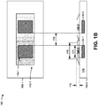
- Figs. 1A and 1B are diagrams of an example 100 of a dielectric based optical filter coating, as described herein.
- example 100 includes a substrate 110, a photodiode 120, a photoresist layer 130, a filter coating layer 140, and a transition area 150.
- the dielectric based optical filter coating is manufactured on substrate 110, which may be an active device wafer, using a lift-off process.
- the lift-off process may be selected based on a difficulty in chemical etching, physical etching, or the like.
- Photoresist layer 130 is disposed onto regions of substrate 110 where filter coating layer 140 is not to be deposited. For example, based on filter coating layer 140 being intended to be deposited to cover photodiode 120 or another type of sensor element, photoresist layer 130 is disposed on portions of substrate 110 that are not aligned to photodiode 120.
- a lift-off process is performed to remove photoresist layer 130, resulting in filter coating layer 140 remaining at the portion of substrate 110 aligned to photodiode 120.
- the lift-off process results in transition area 150 where filter coating layer 140 is associated with a tapered edge of reducing physical thickness. Transition area 150 may be associated with a width of between approximately two and three times a thickness of filter coating layer 140.
- a set ofphotodiodes 120-1 and 120-2 may be positioned in substrate 110, and may be covered by a set of filter coating layers 140-1 and 140-2 such that filter coating layer 140-1 overlaps with filter coating layer 140-2.
- Overlapping filter coating layers 140 reduces a spacing between photodiode 120-1 and photodiode 120-2 relative to separating filter coating layers 140.
- filter coating layers 140 are associated with a thickness 172, a photodiode area 174 (e.g., an area that is aligned with a corresponding photodiode 120, and a functional area 176 (e.g., an area that is disposed between tapered edges of the particular filter coating layer 140).
- Photodiodes 120 may be associated with a separation width 178 (e.g., a spacing between photodiodes 120). Separation width 178 may be greater than three times thickness 172. In this case, thickness 172 is greater than approximately 5 micrometers ( ⁇ m) resulting in separation width 178 being great than approximately 15 ⁇ m. However, it may be advantageous to achieve separation widths between photodiodes of less than 15 ⁇ m, less than 10 ⁇ m, less than 5 ⁇ m, less than 1 ⁇ m, or the like.
- FIGS. 1A and 1B are provided merely as an example. Other examples are possible and may differ from what was described with regard to Figs. 1A and 1B .
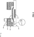
- Fig. 2 is a diagram of an example 200 of an induced transmission filter (ITF) based optical filter coating, as described herein.
- example 200 includes a substrate 210, a photodiode 220, a photoresist layer 230, a filter coating layer 240, which includes a metal layer 240', and a transition area 250.
- ITF induced transmission filter
- metal layer 240' may include a silver (Ag) layer, an aluminum (Al) layer, or the like.
- Metal layer 240' may be encapsulated by a dielectric portion of filter coating layer 240 that reduces a likelihood of corrosion relative to exposing metal layer 240'.
- the tapered edge of filter coating layer 240 is manufactured to have less than a threshold internal angle 260, such as less than approximately 5 degrees.
- the ITF based optical filter coating may be less than approximately 1000 nanometers (nm) in thickness, such as approximately 500 nm, but based on threshold internal angle 260 being less than approximately 5 degrees, transition area 250 may be approximately 10 ⁇ m to 20 ⁇ m, which may correspond to a spacing between photodiodes 220 of between approximately 10 ⁇ m to 20 ⁇ m. This may be larger than is advantageous for sensor element arrays that are to include sensor elements, such as photodiodes 220, that are sized between approximately 2 ⁇ m and 50 ⁇ m and are to be associated with a spacing of between approximately 0.5 ⁇ m and 10 ⁇ m.
- Fig. 2 is provided merely as an example. Other examples are possible and may differ from what was described with regard to Fig. 2 .
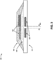
- Fig. 3 is a diagram of an overview of an example implementation 300.
- Example implementation 300 illustrates a single cavity Fabry-Perot filter based optical filter coating, as described herein, that is associated with a spacing of less than a threshold value for sensor elements of a sensor element array, such as a spacing of less than approximately 10 ⁇ m, less than approximately 5 ⁇ m, less than approximately 1 ⁇ m, or the like.
- example implementation 300 includes a substrate 310, a set of photodiodes 320, a first mirror layer 330, a set of spacer layers 340, a second mirror layer 350. Photodiodes 320 are associated with a spacing of separation width 360.
- substrate 310 may be associated with a wafer width of between approximately 50 millimeters (mm) and 500 mm, such as an approximately 100 mm width, an approximately 150 mm width, an approximately 200 mm width, an approximately 300 mm width, an approximately 450 mm width, or the like. In some implementations, substrate 310 may be associated with a thickness of between approximately 50 ⁇ m and 1.0 mm. In some implementations, when substrate 310 is associated with a back-illuminated photodiode 320, substrate 310 may be associated with thickness of between approximately 5 ⁇ m and 70 ⁇ m, between approximately 25 ⁇ m and 50 ⁇ m, or the like, which may be, for example, temporarily bonded to a carrier wafer of another thickness.
- mm millimeters
- 500 mm such as an approximately 100 mm width, an approximately 150 mm width, an approximately 200 mm width, an approximately 300 mm width, an approximately 450 mm width, or the like.
- substrate 310 may be associated with a thickness of between approximately 50
- photodiodes 320 may be associated with a width of between approximately 1 ⁇ m and 20 ⁇ m.
- a mirror such as first mirror layer 330 or second mirror layer 350 may be associated with a thickness of between approximately 20 nanometers (nm) and 80 nm.
- spacer layers 340 may be associated with a thickness of between approximately 15 nm and 300 nm.
- first mirror layer 330 and second mirror layer 350 sandwich a set of spacer layers 340.
- Spacer layers 340 may be deposited using a physical vapor deposition procedure, a chemical vapor deposition procedure, or the like to vary thicknesses of the set of spacer layers 340 and channels formed thereby. Based on varying thicknesses of the set of spacer layers 340, each photodiode 320, or another type of sensor element, is exposed to corresponding varying center wavelengths of light. In this way, an optical filter coating may be manufactured that permits separation width 360 to be less than a threshold value, such as less than 10 ⁇ m, less than 5 ⁇ m, less than 1 ⁇ m, less than 500 nm, or the like. In some implementations, separation width 360 may be between approximately 0.5 ⁇ m and 10 ⁇ m. In some implementations, separation width 360 may be approximately 150 nm.
- Fig. 3 is provided merely as an example. Other examples are possible and may differ from what was described with regard to Fig. 3 .
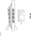
- Figs. 4A-4E are diagrams of example implementations 400/400'/400" of a single cavity Fabry-Perot filter based optical filter coating, as described herein.
- example implementation 400 includes a substrate 410, a set of photodiodes 420-1 to 420-4, a first mirror layer 430, a set of spacer layers 440-1 to 440-4, and a second mirror layer 450.
- first mirror layer 430 and second mirror layer 450 may be quarterwave stacks using layers of silicon dioxide (SiO2) and hydrogenated silicon (Si:H or Si_H).
- the quarterwave stacks may utilize another set of materials, such as another high refractive index material (e.g., niobium pentoxide (Nb2O5), tantalum pentoxide (Ta2O5), titanium dioxide (TiO2), hafnium dioxide (HfO2) a combination thereof, or the like), another low refractive index material (e.g., magnesium fluoride (MgF2) or the like), or the like.
- another high refractive index material e.g., niobium pentoxide (Nb2O5), tantalum pentoxide (Ta2O5), titanium dioxide (TiO2), hafnium dioxide (HfO2) a combination thereof, or the like
- another low refractive index material e.g., magnesium fluoride (MgF2) or the
- a non-fluoride based material may be preferred to reduce a difficulty of deposition.
- a material with associated with a relatively higher effective index may be preferred to reduce an angle-shift, to reduce a quantity of layers of a blocker or mirror, or the like.
- Spacer layers 440 may be spacers manufactured using one or more layers of hydrogenated silicon.
- spacer layers 440 may include another material, such as Nb2O5, Ta2O5, TiO2, HfO2, another type of oxide, a combination thereof, or the like.
- First mirror layer 430 and/or second mirror layer 450 may be disposed in alignment with sensor elements, such as photodiodes 420.
- semi-transparent metal mirrors may be used rather than quarterwave stacks, as described herein.
- a metal mirror including a silver (Ag) layer may be used for an ultraviolet (UV)-A spectral range, a visible spectral range, a near infrared spectral range (NIR), or the like.
- a metal mirror including an aluminum (Al) layer may be used for a UV spectral range or the like (approximately 200 nm to 400 nm range).
- first mirror layer 430 may include a blocker layer disposed on a surface of first mirror layer 430, a protective layer disposed on a surface of first mirror layer 430, or the like.
- Each spacer layer 440 is associated with a particular thickness that corresponds to a particular center wavelength of light being passed to a corresponding photodiode 420 or another type of sensor element.
- spacer layer 440-1 may be associated with a thickness of approximately 96.6 nm
- spacer layer 440-2 may be associated with a thickness of approximately 115.3 nm
- spacer layer 440-3 may be associated with a thickness of approximately 131.5 nm
- spacer layer 440-4 may be associated with a thickness of approximately 147.6 nm.
- each spacer layer 440 may be deposited onto first mirror layer 430 using a set of patterning and coating steps for each spacer layer 440.
- second mirror layer 450 may be deposited onto exposed portions of first mirror layer 430 and spacer layers 440, thereby encapsulating spacer layers 440 with first mirror layer 430. In this way, a spacing between photodiodes 220 or other sensor elements of between approximately 600 nm and 10 ⁇ m, less than approximately 600 nm, or the like may be achieved.
- spacer layers 440 may be deposited using a physical vapor deposition (PVD) procedure.
- PVD physical vapor deposition
- spacer layers 440 and/or other portions of implementations described herein may be manufactured using a magnetron sputtering procedure, an e-beam and thermal evaporation procedure, and/or the like.
- spacer layers 440 may be deposited using a chemical vapor deposition (CVD) procedure.
- PVD physical vapor deposition
- a thickness of spacer layers 440 may be selected to achieve a particular spectral range of light, such as a UV spectral range (e.g., approximately 200 nm to 400 nm), a visible spectral range (e.g., approximately 400 nm to 700 nm), an NIR spectral range (e.g., approximately 700 nm to 2000 nm), a mid-wavelength IR (MWIR) spectral range (e.g., approximately 2 ⁇ m to 6 ⁇ m), a low-wavelength IR (LWIR) spectral range (e.g., approximately 6 ⁇ m to 14 ⁇ m), or the like.
- the thicknesses of layers may be related to a desired spectral range.
- thicknesses of mirror layers 430 or 450 may be between approximately 20 nm and 400 nn
- spacer layers 440 may be between approximately 15 nm and 1500 nm, or the like.
- spacer layers 440 may be deposited to manufacture a silicon-based detector, an indium gallium arsenide (InGaAs)-based detector, or the like.
- spacer layers 440 may be deposited for a hyperspectral imaging sensor.
- spacer layers 440 may be deposited for a back-illuminated sensor or a front-illuminated sensor.
- a similar example implementation 400' includes a substrate 410, a set of photodiodes 420-1 to 420-4, a first mirror layer 430, a set of spacer layers 440-1 to 440-4, and a second mirror layer 450.
- spacer layer 440-1 is deposited to cover all of first mirror layer 430 and each photodiode 420, and each other spacer layer 440 is deposited onto spacer layer 440-1.
- example implementation 400' is associated with a reduced quantity of patterning and coating steps that are to be performed to deposit spacer layers 440 relative to the patterning and coating steps that are performed to deposit spacer layers 440 of example implementation 400.
- a mirror layer such as mirror layer 430
- a metal mirror layer e.g., a silver based material
- a spacer layer such as spacer layer 440-1, may provide a protective coating of the metal mirror layer.
- each of spacer layers 440-2 to 440-4 may be patterned and coated onto first mirror layer 430, and spacer layer 440-1 may be deposited onto exposed portions of first mirror layer 430 and each of spacer layers 440-2 to 440-4 before depositing second mirror layer 450.
- an entire surface of first spacer layer 440-1 is disposed contiguous to the surface of second mirror layer 450 rather than contiguous to first mirror layer 430.
- each of spacer layers 440-2 to 440-4 is associated with a particular thickness in addition to the thickness of spacer layer 440-1 (e.g., approximately 96.6 nm).
- spacer layer 440-2 is associated with an additional thickness of approximately 18.7 nm
- spacer layer 440-3 is associated with an additional thickness of approximately 34.9 nm
- spacer layer 440-4 is associated with an additional thickness of approximately 51 nm.
- a similar example implementation 400" includes a substrate 410, a set of photodiodes 420-1 to 420-4, a first mirror layer 430, a set of spacer layers 440-1 to 440-4, and a second mirror layer 450.
- spacer layer 440-1 is deposited onto first mirror layer 430 and covers each ofphotodiodes 420-1 to 420-4.
- spacer layer 440-2 is deposited onto a portion of spacer layer 440-1 and covers each of photodiodes 420-2 to 420-4.
- spacer layer 440-3 is deposited onto a portion of spacer layer 440-2 and covers a subset of photodiodes 420 (e.g., each of photodiodes 420-3 to 420-4).
- spacer layer 440-4 is deposited onto a portion of spacer layer 440-3 and covers photodiode 420-4.
- example implementation 400 reduces a quantity of patterning and coating steps that are to be performed to deposit spacer layers 440 in example implementation 400.
- each of spacer layers 440-2 to 440-4 is associated with a thickness in addition to the thickness of a previous spacer layer 440.
- spacer layer 440-2 is associated with an additional thickness of approximately 18.7 nm deposited onto spacer layer 440-1 (e.g., which is associated with a thickness of approximately 96.6 nm)
- spacer layer 440-3 is associated with an additional thickness of approximately 16.2 nm deposited onto spacer layer 440-2
- spacer layer 440-4 is associated with an additional thickness of approximately 16.1 nm deposited onto spacer layer 440-3.
- a spacing between photodiodes 220 or other sensor elements of between approximately 150 nm and 2 ⁇ m, less than approximately 150 nm, or the like may be achieved.
- a chart 470 identifies a set of optical characteristics relating to channels of example implementations 400/400'/400". For example, for a first channel associated with spacer layer 440-1 and photodiode 420-1, a thickness of spacer layer 440-1 results in a center wavelength of approximately 795 nm. Similarly, for a second channel associated with spacer layer 440-2 and photodiode 420-2, a thickness of spacer layer 440-2 results in a center wavelength of approximately 870 nm. Similarly, for a third channel associated with spacer layer 440-3 and photodiode 420-3, a thickness of spacer layer 440-3 results in a center wavelength of approximately 935 nm.
- a thickness of spacer layer 440-4 results in a center wavelength of approximately 1000 nm.
- a chart 480 identifies a set of physical characteristics relating example implementations 400/400'/400".
- a mirror such as mirror layer 430 or mirror layer 450
- a spacer layer such as spacer layer 440-4
- mirror layers may be associated with multiple layers.
- mirror layers may include Si:H layers, SiO2 layers, etc.
- FIGS. 4A-4E are provided merely as examples. Other examples are possible and may differ from what was described with regard to Figs. 4A-4E .
- Figs. 5A-5E are diagrams of an example implementation 500 of an optical filter coating for a depth sensing system, as described herein.
- example implementation 500 includes a substrate 510 (e.g., silicon nitride (S3N4) or in another example SiO2 or Si), a set of zinc oxide (ZnO) layers 520-1 to 520-4, a set of silver (Ag) layers 530-1 to 530-2, a set of niobium titanium oxide (NbTiOx) layers 540-1 to 540-3, and a set of silicon dioxide (SiO2) layers 550-1 to 550-2.
- the optical filter coating of example implementation 500 may be a Fabry-Perot optical filter.
- another example may include a transparent substrate 510 that is bonded to a sensor device.
- ZnO layers 520 may be each associated with a thickness of approximately 1.5 nm.
- Ag layers 530 which are a set of semi-transparent metal mirrors encapsulating a set of spacer layers formed by NbTiOx 540-1, are associated with a thickness of approximately 40 nm.
- NbTiOx 540-1 may correspond to the spacers 440 in Figs. 4A-4C , resulting in differing thicknesses for NbTiOx 540-1 corresponding to a spacer thickness that is desired.
- NbTiOx 540-1 may form a set of three channels for visible light (e.g., red/green/blue (RGB) light) detection for image sensing and a fourth channel (e.g., IR and blue light) for depth sensing (e.g., three-dimensional depth sensing).
- the four channels may correspond to spacers 440-1 through 440-4 shown in Figs. 4A-4C .
- a first channel for blue visible light detection may be associated with a total thickness of approximately 44.8 nm
- a second channel for green visible light detection may be associated with a total thickness of approximately 60.5 nm
- a third channel for red visible light detection may be associated with a total thickness of approximately 82.9 nm
- the fourth channel for IR and blue light detection i.e., depth sensing
- layers of NbTiOx 540-1 may be deposited in a form as shown in Figs. 4A-4C .
- each channel may be a separate filter layer stack, each channel may share a common first filter layer, each channel may be deposited on a portion of a previously deposited filter layer, or the like.
- depositing at least one layer common to each channel may improve durability of Ag layers 530 by providing a protective layer.
- NbTiOx layer 540-2 may be associated with a thickness of approximately 50 nm
- SiO2 layer 550-1 may be associated with a thickness of approximately 18 nm
- NbTiOx layer 540-3 may be associated with a thickness of approximately 16 nm
- SiO2 layer 550-2 may be associated with a thickness of approximately 101 nm.
- Layers 540-2, 550-1, 540-3, and 550-2 may collectively form an anti-reflection coating for sensor elements embedded in substrate 510 or disposed onto substrate 510.
- a chart 570 identifies a set of optical characteristics relating to channels of example implementation 500.
- the first channel associated with red visible light sensing is associated with a center wavelength of approximately 620 nm.
- the second channel associated with green visible light sensing is associated with a center wavelength of approximately 520 nm.
- the third channel associated with blue visible light sensing is associated with a center wavelength of approximately 450 nm.
- the fourth channel associated with depth sensing e.g., blue light and IR lights sensing
- a diagram 580 identifies a sensor element array of sensor elements relating to example implementation 500.
- the sensor element array e.g., a complimentary metal-oxide-semiconductor (CMOS) technology, a charge-coupled device (CCD) technology, or the like
- the sensor element array includes a set of first channels (e.g., red light channels, identified as R), a second of second channels (e.g., green light channels, identified as G), a set of third channels (e.g., blue light channels, identified as B), and a set of fourth channels (e.g., IR and blue light channels, identified as IR/B).
- first channels e.g., red light channels, identified as R
- second of second channels e.g., green light channels, identified as G
- a set of third channels e.g., blue light channels, identified as B
- fourth channels e.g., IR and blue light channels, identified as IR/B
- spacer layers for the sensor element array are manufactured by depositing each spacer layer on a portion of the previous spacer layer, as described herein with regard to Fig. 4C .
- the sensor elements may be back illuminated sensor elements to provide an improved quantum efficiency and spectral response reproducibility relative to another configuration of sensor elements.
- a dielectric blocker may be applied to the IR/B channels with a thickness of approximately 750 nm, resulting in a spacing of approximately 2 ⁇ m.
- diagram 580 depicts a sensor element array with 64 channels
- implementations, described herein may be used with another quantity of channels less than a threshold, such as less than or equal to 64 channels (e.g., 64 channels, 63 channels, 62 channels, ..., 2 channels, etc.), less than or equal to 32 channels, less than or equal to 16 channels, less than or equal to 8 channels, less than or equal to 4 channels, or the like.
- another quantity of sensor elements i.e., pixels
- implementations described herein may be utilized for a pixel count of between approximately 10 million pixels and 40 million pixels, between approximately 250 thousand pixels and 40 million pixels, or the like. Additionally, or alternatively, implementations described herein may be utilized for a pixel count greater than approximately 250 thousand, a pixel count greater than approximately 1 million, a pixel count greater than approximately 4 million, a pixel count greater than approximately 20 million, or the like.
- a diagram 590 and a diagram 590' are provided to identify example optical characteristics relating to an angle shift of sensor elements.
- Diagrams 590 and 590' show an angle shift of sensor elements.
- diagram 590 may be associated with using a mixed spacer configuration for a near-infrared filter (e.g., an approximately 44.8 nm niobium-titanium-oxide (NbTiOx) and an approximately 42 nm Si:H spacer).
- the mixed spacer configuration may include another first material (e.g., another oxide) for one or more first layers and another second material for one or more second layers.
- Diagram 590 may be associated with an optical filter utilizing a set of coatings described in Fig.
- Diagram 590' may be associated with using a spacer configuration similar to example implementation 500.
- Diagram 590' may be associated with an optical filter utilizing a set of coatings described in Fig. 5E and by diagram 595'.
- the optical filter of diagram 590 and the optical filter of diagram 590' are associated with similar stackups for a red channel, a green channel, and a blue channel, but are associated with different stackups for an NIR channel.
- the optical filter of diagram 590 is associated with a hydrogenated-silicon layer that blocks a second order peak, as described herein.
- sensor elements associated with the optical filter of diagram 590 receiving NIR light exhibit a reduced angle shift and an improved transmissivity relative to sensor elements associated with the optical filter of diagram 590'.
- angle shift is reduced and transmissivity is improved for sensor elements utilizing the optical filter of diagram 590 relative to sensor elements using the optical filter of diagram 590'.
- a blocker is not needed to suppress a second order peak for sensor elements utilizing the optical filter of diagram 590.
- FIGS. 5A-5E are provided merely as examples. Other examples are possible and may differ from what was described with regard to Figs. 5A-5E .
- an optical filter may be manufactured for a sensor element array with a spacing of less than approximately 10 ⁇ m, 5 ⁇ m, 1 ⁇ m, 500 nm, 200 nm, 150 nm, or the like. Moreover, the optical filter may be associated with a reduced angle shift and an improved transmissivity relative to another type optical filter.
- the term component is intended to be broadly construed as hardware, firmware, and/or a combination of hardware and software.
- satisfying a threshold may refer to a value being greater than the threshold, more than the threshold, higher than the threshold, greater than or equal to the threshold, less than the threshold, fewer than the threshold, lower than the threshold, less than or equal to the threshold, equal to the threshold, etc.
Landscapes
- Physics & Mathematics (AREA)
- Spectroscopy & Molecular Physics (AREA)
- General Physics & Mathematics (AREA)
- Optics & Photonics (AREA)
- Engineering & Computer Science (AREA)
- Manufacturing & Machinery (AREA)
- Light Receiving Elements (AREA)
- Solid State Image Pick-Up Elements (AREA)
- Optical Filters (AREA)
- Optical Elements Other Than Lenses (AREA)
- Spectrometry And Color Measurement (AREA)
- Surface Treatment Of Optical Elements (AREA)
- Optical Integrated Circuits (AREA)
- Optical Head (AREA)
Abstract
Description
- In an optical device, such as a sensor element array, sensor elements may be associated with a particular spacing. For example, a first sensor element may be associated with a particular spacing from a second sensor element. The sensor elements may be associated with a size of between approximately 50 micrometers (µm) and 200 µm. The spacing between a pair of sensor elements may be greater than approximately 20 µm. A sensor element array may be used for a sensing system, such as a three-dimensional depth sensing system or the like.
- According to some possible implementations, a device may include a filter array disposed on a substrate. The filter array may include a first mirror disposed on the substrate. The filter array may include a plurality of spacers disposed on the first mirror. A first spacer, of the plurality of spacers, may be associated with a first thickness. A second spacer, of the plurality of spacers, may be associated with a second thickness that is different from the first thickness. A first channel corresponding to the first spacer and a second channel corresponding to the second spacer may be associated with a separation width of less than approximately 10 micrometers (µm). The filter array may include a second mirror disposed on the plurality of spacers.
- The second mirror may be aligned with two or more sensor elements of a set of sensor elements.
- The plurality of spacers may be deposited onto the substrate using at least one of: a physical vapor deposition (PVD) process, a chemical vapor deposition (CVD) process, or a lift-off process.
- The first thickness or the second thickness may be selected to pass through a particular spectral range of light, the particular spectral range including at least one of: an ultraviolet (UV) spectral range, a visible spectral range, a near infrared (NIR) spectral range, a mid-wavelength infrared (MWIR) spectral range, or a low-wavelength infrared (LWIR) spectral range.
- The device may be a silicon-based detector or an indium gallium arsenide (InGaAS)-based detector.
- The device may be a hyperspectral imaging sensor with less than a threshold quantity of channels.
- The first mirror or the second mirror may be a metal mirror including a silver layer or an aluminum layer.
- The first mirror or the second mirror may be a quarterwave stack including a low refractive index material and a high refractive index material, the low refractive index material including at least one of: a magnesium fluoride (MgF2) layer, or a silicon oxide (SiO2) layer.
- The first mirror or the second mirror may be a quarterwave stack including a low refractive index material and a high refractive index material, the high refractive index material including at least one of: a hydrogenated silicon (Si:H) layer, a niobium pentoxide (Nb2O5) layer, a tantalum pentoxide (Ta2O5) layer, a titanium dioxide (TiO2) layer, or a hafnium dioxide (HfO2) layer.
- The plurality of spacers may include at least one of: a hydrogenated silicon (Si:H) layer, a niobium pentoxide (Nb2O5) layer, a tantalum pentoxide (Ta2O5) layer, a titanium dioxide (TiO2) layer, or a hafnium oxide (HfO2) layer.
- According to some possible implementations, a device may include a filter array disposed on a substrate. The filter array may include a first mirror disposed on the substrate. The filter array may include a spacer disposed on the first mirror. The spacer may include a plurality of spacer layers. A first spacer layer, of the plurality of spacer layers, may be disposed to cover the first mirror. A second spacer layer, of the plurality of spacer layers, may be disposed onto the first spacer layer. A first channel corresponding to the first spacer layer and a second channel corresponding to the second spacer layer may be associated with a separation width of less than approximately 5 micrometers (µm). The filter array may include a second mirror disposed on the spacer.
- The spacer may further comprise: a third spacer layer, of the plurality of spacer layers, disposed onto the first spacer layer, the third spacer layer and the second spacer layer not being contiguous.
- The filter array may be aligned to a sensor element array, the sensor element array being a hyperspectral imaging sensor including a plurality of sensor elements, the plurality of sensor elements being associated with between approximately 250 thousand pixels and 40 million pixels.
- The separation width may be less than approximately 500 nanometers (nm).
- The filter array may include at least one of: a blocker layer, or an anti-reflection coating layer.
- According to some possible implementations, a device may include a filter array disposed on a substrate. The substrate may be a glass substrate to be bonded to a sensor element array or a silicon substrate including the sensor element array. The filter array may include a first mirror disposed on the substrate. The filter array may include a plurality of spacer layers. A first spacer layer, of the plurality of spacer layers, may be disposed onto the first mirror and covering a set of sensor elements of the sensor element array. A second spacer layer, of the plurality of spacer layers, may be disposed onto the first spacer layer and covering a subset of the set of sensor elements. A third spacer layer, of the plurality of spacer layers, may be disposed onto the second spacer layer and covering a subset of the subset of sensor elements. Each sensor element, of the set of sensor elements, may be associated with a spacing of less than approximately 1 micrometer (µm). The filter array may include a second mirror disposed on the plurality of spacer layers. The second mirror may be aligned with the set of sensor elements.
- The set of sensor elements may comprise: a complimentary metal-oxide-semiconductor (CMOS) technology, or a charge-coupled device (CCD) technology.
- The device may further comprise: a fourth spacer layer, of the plurality of spacer layers, disposed onto the third spacer layer and covering a subset of the subset of the subset of sensor elements.
- The device may be a red-green-blue-infrared (RGB, IR/B) depth sensing system; the RGB IR/B depth sensing system including a set of red channels, a set of green channels, a set of blue channels, and a set of infrared channels formed by the plurality of spacer layers.
- The set of infrared channels may be associated with a mixed spacer configuration, the mixed spacer configuration including one or more niobium-titanium-oxide (NbTiOx) based layers and one or more hydrogenated silicon (Si:H) based layers.
-
-
Figs. 1A and1B are diagrams of an example of a dielectric based optical filter coating, as described herein; -
Fig. 2 is a diagram of an example of an induced transmission filter (ITF) based optical filter coating, as described herein; -
Fig. 3 is a diagram of an overview of an example implementation, as described herein; -
Figs. 4A-4E are diagrams of an example implementation an optical filter coating, as described herein; and -
Figs. 5A-5E are diagrams of an example implementation of an optical filter coating for a depth sensing system, as described herein. - The following detailed description of example implementations refers to the accompanying drawings. The same reference numbers in different drawings may identify the same or similar elements.
- In an optical device, such as a sensor element array, sensor elements may be spaced by a particular distance. The sensor elements may be associated with a size of between approximately 50 micrometers (µm) and 200 µm. Spacing between a pair of sensor elements may be greater than approximately 20 µm. However, as quantities of sensor elements included in a single optical device increase and/or as package sizes for optical devices decrease, it may be advantageous to manufacture sensor element arrays of sensor elements with a spacing of less than approximately 20 µm, less than approximately 10 µm, less than approximately 1 µm, or the like. Implementations, described herein, may provide an optical filter to enable a sensor element array of sensor elements with a spacing of less than a threshold value, such as less than approximately 20 µm, less than approximately 10 µm, less than approximately 1 µm, or the like.
-
Figs. 1A and1B are diagrams of an example 100 of a dielectric based optical filter coating, as described herein. As shown inFig. 1A , example 100 includes asubstrate 110, aphotodiode 120, aphotoresist layer 130, afilter coating layer 140, and atransition area 150. - With regard to
Fig. 1A , the dielectric based optical filter coating is manufactured onsubstrate 110, which may be an active device wafer, using a lift-off process. The lift-off process may be selected based on a difficulty in chemical etching, physical etching, or the like.Photoresist layer 130 is disposed onto regions ofsubstrate 110 wherefilter coating layer 140 is not to be deposited. For example, based onfilter coating layer 140 being intended to be deposited to coverphotodiode 120 or another type of sensor element,photoresist layer 130 is disposed on portions ofsubstrate 110 that are not aligned to photodiode 120. After deposition offilter coating layer 140 ontophotoresist layer 130 and an exposed portion ofsubstrate 110 that is aligned withphotodiode 120, a lift-off process is performed to removephotoresist layer 130, resulting infilter coating layer 140 remaining at the portion ofsubstrate 110 aligned tophotodiode 120. However, the lift-off process results intransition area 150 wherefilter coating layer 140 is associated with a tapered edge of reducing physical thickness.Transition area 150 may be associated with a width of between approximately two and three times a thickness offilter coating layer 140. - As shown in
Fig. 1B , in a top-view 160-1 and a side-view 160-2, a set ofphotodiodes 120-1 and 120-2 may be positioned insubstrate 110, and may be covered by a set of filter coating layers 140-1 and 140-2 such that filter coating layer 140-1 overlaps with filter coating layer 140-2. Overlapping filter coating layers 140 reduces a spacing between photodiode 120-1 and photodiode 120-2 relative to separating filter coating layers 140. In this case, filter coating layers 140 are associated with athickness 172, a photodiode area 174 (e.g., an area that is aligned with acorresponding photodiode 120, and a functional area 176 (e.g., an area that is disposed between tapered edges of the particular filter coating layer 140).Photodiodes 120 may be associated with a separation width 178 (e.g., a spacing between photodiodes 120).Separation width 178 may be greater than threetimes thickness 172. In this case,thickness 172 is greater than approximately 5 micrometers (µm) resulting inseparation width 178 being great than approximately 15 µm. However, it may be advantageous to achieve separation widths between photodiodes of less than 15 µm, less than 10 µm, less than 5 µm, less than 1 µm, or the like. - As indicated above,
Figs. 1A and1B are provided merely as an example. Other examples are possible and may differ from what was described with regard toFigs. 1A and1B . -
Fig. 2 is a diagram of an example 200 of an induced transmission filter (ITF) based optical filter coating, as described herein. As shown inFig. 2 , example 200 includes asubstrate 210, aphotodiode 220, aphotoresist layer 230, afilter coating layer 240, which includes a metal layer 240', and atransition area 250. - With regard to
Fig. 2 , metal layer 240' may include a silver (Ag) layer, an aluminum (Al) layer, or the like. Metal layer 240' may be encapsulated by a dielectric portion offilter coating layer 240 that reduces a likelihood of corrosion relative to exposing metal layer 240'. In this case, to manufacturefilter coating layer 240 to provide protective encapsulation, the tapered edge offilter coating layer 240 is manufactured to have less than a thresholdinternal angle 260, such as less than approximately 5 degrees. The ITF based optical filter coating may be less than approximately 1000 nanometers (nm) in thickness, such as approximately 500 nm, but based on thresholdinternal angle 260 being less than approximately 5 degrees,transition area 250 may be approximately 10 µm to 20 µm, which may correspond to a spacing betweenphotodiodes 220 of between approximately 10 µm to 20 µm. This may be larger than is advantageous for sensor element arrays that are to include sensor elements, such asphotodiodes 220, that are sized between approximately 2 µm and 50 µm and are to be associated with a spacing of between approximately 0.5 µm and 10 µm. - As indicated above,
Fig. 2 is provided merely as an example. Other examples are possible and may differ from what was described with regard toFig. 2 . -
Fig. 3 is a diagram of an overview of anexample implementation 300.Example implementation 300 illustrates a single cavity Fabry-Perot filter based optical filter coating, as described herein, that is associated with a spacing of less than a threshold value for sensor elements of a sensor element array, such as a spacing of less than approximately 10 µm, less than approximately 5 µm, less than approximately 1 µm, or the like. As shown inFig. 3 ,example implementation 300 includes asubstrate 310, a set ofphotodiodes 320, afirst mirror layer 330, a set of spacer layers 340, asecond mirror layer 350.Photodiodes 320 are associated with a spacing ofseparation width 360. - In some implementations,
substrate 310 may be associated with a wafer width of between approximately 50 millimeters (mm) and 500 mm, such as an approximately 100 mm width, an approximately 150 mm width, an approximately 200 mm width, an approximately 300 mm width, an approximately 450 mm width, or the like. In some implementations,substrate 310 may be associated with a thickness of between approximately 50 µm and 1.0 mm. In some implementations, whensubstrate 310 is associated with a back-illuminatedphotodiode 320,substrate 310 may be associated with thickness of between approximately 5 µm and 70 µm, between approximately 25 µm and 50 µm, or the like, which may be, for example, temporarily bonded to a carrier wafer of another thickness. - In some implementations,
photodiodes 320 may be associated with a width of between approximately 1 µm and 20 µm. In some implementations, a mirror, such asfirst mirror layer 330 orsecond mirror layer 350 may be associated with a thickness of between approximately 20 nanometers (nm) and 80 nm. In some implementations, spacer layers 340 may be associated with a thickness of between approximately 15 nm and 300 nm. - With regard to
Fig. 3 ,first mirror layer 330 andsecond mirror layer 350 sandwich a set of spacer layers 340. Spacer layers 340 may be deposited using a physical vapor deposition procedure, a chemical vapor deposition procedure, or the like to vary thicknesses of the set of spacer layers 340 and channels formed thereby. Based on varying thicknesses of the set of spacer layers 340, eachphotodiode 320, or another type of sensor element, is exposed to corresponding varying center wavelengths of light. In this way, an optical filter coating may be manufactured that permitsseparation width 360 to be less than a threshold value, such as less than 10 µm, less than 5 µm, less than 1 µm, less than 500 nm, or the like. In some implementations,separation width 360 may be between approximately 0.5 µm and 10 µm. In some implementations,separation width 360 may be approximately 150 nm. - As indicated above,
Fig. 3 is provided merely as an example. Other examples are possible and may differ from what was described with regard toFig. 3 . -
Figs. 4A-4E are diagrams ofexample implementations 400/400'/400" of a single cavity Fabry-Perot filter based optical filter coating, as described herein. As shown inFig. 4A ,example implementation 400 includes asubstrate 410, a set of photodiodes 420-1 to 420-4, afirst mirror layer 430, a set of spacer layers 440-1 to 440-4, and asecond mirror layer 450. - With regard to
Fig. 4A ,first mirror layer 430 andsecond mirror layer 450 may be quarterwave stacks using layers of silicon dioxide (SiO2) and hydrogenated silicon (Si:H or Si_H). In another example, the quarterwave stacks may utilize another set of materials, such as another high refractive index material (e.g., niobium pentoxide (Nb2O5), tantalum pentoxide (Ta2O5), titanium dioxide (TiO2), hafnium dioxide (HfO2) a combination thereof, or the like), another low refractive index material (e.g., magnesium fluoride (MgF2) or the like), or the like. In some implementations, a non-fluoride based material may be preferred to reduce a difficulty of deposition. In some implementations, a material with associated with a relatively higher effective index may be preferred to reduce an angle-shift, to reduce a quantity of layers of a blocker or mirror, or the like. Spacer layers 440 may be spacers manufactured using one or more layers of hydrogenated silicon. In another example, spacer layers 440 may include another material, such as Nb2O5, Ta2O5, TiO2, HfO2, another type of oxide, a combination thereof, or the like.First mirror layer 430 and/orsecond mirror layer 450 may be disposed in alignment with sensor elements, such as photodiodes 420. - In another example, semi-transparent metal mirrors may be used rather than quarterwave stacks, as described herein. For example, a metal mirror including a silver (Ag) layer may be used for an ultraviolet (UV)-A spectral range, a visible spectral range, a near infrared spectral range (NIR), or the like. Similarly, a metal mirror including an aluminum (Al) layer may be used for a UV spectral range or the like (approximately 200 nm to 400 nm range).
- In some implementations,
first mirror layer 430 may include a blocker layer disposed on a surface offirst mirror layer 430, a protective layer disposed on a surface offirst mirror layer 430, or the like. Each spacer layer 440 is associated with a particular thickness that corresponds to a particular center wavelength of light being passed to a corresponding photodiode 420 or another type of sensor element. For example, as shown in table 460, spacer layer 440-1 may be associated with a thickness of approximately 96.6 nm, spacer layer 440-2 may be associated with a thickness of approximately 115.3 nm, spacer layer 440-3 may be associated with a thickness of approximately 131.5 nm, and spacer layer 440-4 may be associated with a thickness of approximately 147.6 nm. In this case, each spacer layer 440 may be deposited ontofirst mirror layer 430 using a set of patterning and coating steps for each spacer layer 440. As shown,second mirror layer 450 may be deposited onto exposed portions offirst mirror layer 430 and spacer layers 440, thereby encapsulating spacer layers 440 withfirst mirror layer 430. In this way, a spacing betweenphotodiodes 220 or other sensor elements of between approximately 600 nm and 10 µm, less than approximately 600 nm, or the like may be achieved. - In some implementations, spacer layers 440 may be deposited using a physical vapor deposition (PVD) procedure. For example, spacer layers 440 and/or other portions of implementations described herein may be manufactured using a magnetron sputtering procedure, an e-beam and thermal evaporation procedure, and/or the like. In some implementations, spacer layers 440 may be deposited using a chemical vapor deposition (CVD) procedure. In some implementations, a thickness of spacer layers 440 may be selected to achieve a particular spectral range of light, such as a UV spectral range (e.g., approximately 200 nm to 400 nm), a visible spectral range (e.g., approximately 400 nm to 700 nm), an NIR spectral range (e.g., approximately 700 nm to 2000 nm), a mid-wavelength IR (MWIR) spectral range (e.g., approximately 2 µm to 6 µm), a low-wavelength IR (LWIR) spectral range (e.g., approximately 6 µm to 14 µm), or the like. The thicknesses of layers may be related to a desired spectral range. For example, for a spectral range of approximately 2 µm to 6 µm or approximately 6 µm to 14 µm, thicknesses of mirror layers 430 or 450 may be between approximately 20 nm and 400 nn, spacer layers 440 may be between approximately 15 nm and 1500 nm, or the like. In some implementations, spacer layers 440 may be deposited to manufacture a silicon-based detector, an indium gallium arsenide (InGaAs)-based detector, or the like. In some implementations, spacer layers 440 may be deposited for a hyperspectral imaging sensor. In some implementations, spacer layers 440 may be deposited for a back-illuminated sensor or a front-illuminated sensor.
- As shown in
Fig. 4B , a similar example implementation 400' includes asubstrate 410, a set of photodiodes 420-1 to 420-4, afirst mirror layer 430, a set of spacer layers 440-1 to 440-4, and asecond mirror layer 450. - With regard to
Fig. 4B , spacer layer 440-1 is deposited to cover all offirst mirror layer 430 and each photodiode 420, and each other spacer layer 440 is deposited onto spacer layer 440-1. In this way, example implementation 400' is associated with a reduced quantity of patterning and coating steps that are to be performed to deposit spacer layers 440 relative to the patterning and coating steps that are performed to deposit spacer layers 440 ofexample implementation 400. In some implementations, when a mirror layer, such asmirror layer 430, is a metal mirror layer (e.g., a silver based material), a spacer layer, such as spacer layer 440-1, may provide a protective coating of the metal mirror layer. In another example, each of spacer layers 440-2 to 440-4 may be patterned and coated ontofirst mirror layer 430, and spacer layer 440-1 may be deposited onto exposed portions offirst mirror layer 430 and each of spacer layers 440-2 to 440-4 before depositingsecond mirror layer 450. In other words, an entire surface of first spacer layer 440-1 is disposed contiguous to the surface ofsecond mirror layer 450 rather than contiguous tofirst mirror layer 430. As shown in table 460', each of spacer layers 440-2 to 440-4 is associated with a particular thickness in addition to the thickness of spacer layer 440-1 (e.g., approximately 96.6 nm). For example, spacer layer 440-2 is associated with an additional thickness of approximately 18.7 nm, spacer layer 440-3 is associated with an additional thickness of approximately 34.9 nm, and spacer layer 440-4 is associated with an additional thickness of approximately 51 nm. - As shown in
Fig. 4C , asimilar example implementation 400" includes asubstrate 410, a set of photodiodes 420-1 to 420-4, afirst mirror layer 430, a set of spacer layers 440-1 to 440-4, and asecond mirror layer 450. - With regard to
Fig. 4C , spacer layer 440-1 is deposited ontofirst mirror layer 430 and covers each ofphotodiodes 420-1 to 420-4. Similarly, spacer layer 440-2 is deposited onto a portion of spacer layer 440-1 and covers each of photodiodes 420-2 to 420-4. Similarly, spacer layer 440-3 is deposited onto a portion of spacer layer 440-2 and covers a subset of photodiodes 420 (e.g., each of photodiodes 420-3 to 420-4). Similarly, spacer layer 440-4 is deposited onto a portion of spacer layer 440-3 and covers photodiode 420-4. In this way,example implementation 400" reduces a quantity of patterning and coating steps that are to be performed to deposit spacer layers 440 inexample implementation 400. As shown in table 460", each of spacer layers 440-2 to 440-4 is associated with a thickness in addition to the thickness of a previous spacer layer 440. For example, spacer layer 440-2 is associated with an additional thickness of approximately 18.7 nm deposited onto spacer layer 440-1 (e.g., which is associated with a thickness of approximately 96.6 nm), spacer layer 440-3 is associated with an additional thickness of approximately 16.2 nm deposited onto spacer layer 440-2, and spacer layer 440-4 is associated with an additional thickness of approximately 16.1 nm deposited onto spacer layer 440-3. In this way, a spacing betweenphotodiodes 220 or other sensor elements of between approximately 150 nm and 2 µm, less than approximately 150 nm, or the like may be achieved. - As shown in
Fig. 4D , achart 470 identifies a set of optical characteristics relating to channels ofexample implementations 400/400'/400". For example, for a first channel associated with spacer layer 440-1 and photodiode 420-1, a thickness of spacer layer 440-1 results in a center wavelength of approximately 795 nm. Similarly, for a second channel associated with spacer layer 440-2 and photodiode 420-2, a thickness of spacer layer 440-2 results in a center wavelength of approximately 870 nm. Similarly, for a third channel associated with spacer layer 440-3 and photodiode 420-3, a thickness of spacer layer 440-3 results in a center wavelength of approximately 935 nm. Similarly, for a fourth channel associated with spacer layer 440-4 and photodiode 420-4, a thickness of spacer layer 440-4 results in a center wavelength of approximately 1000 nm. Although described herein in terms of a particular set of center wavelengths, other center wavelengths are possible and may differ from what was described with regard toFig. 4D . - As shown in
Fig. 4E , achart 480 identifies a set of physical characteristics relatingexample implementations 400/400'/400". For example, a mirror, such asmirror layer 430 ormirror layer 450, may be associated with a thickness of between approximately 40 nm and 500 nm. Similarly, a spacer layer, such as spacer layer 440-4 may be associated with a thickness of approximately 147.61 nm. In some implementations, mirror layers, such asmirror layer 430 ormirror layer 450 may be associated with multiple layers. For example, mirror layers may include Si:H layers, SiO2 layers, etc. - As indicated above,
Figs. 4A-4E are provided merely as examples. Other examples are possible and may differ from what was described with regard toFigs. 4A-4E . -
Figs. 5A-5E are diagrams of anexample implementation 500 of an optical filter coating for a depth sensing system, as described herein. As shown inFig. 5A ,example implementation 500 includes a substrate 510 (e.g., silicon nitride (S3N4) or in another example SiO2 or Si), a set of zinc oxide (ZnO) layers 520-1 to 520-4, a set of silver (Ag) layers 530-1 to 530-2, a set of niobium titanium oxide (NbTiOx) layers 540-1 to 540-3, and a set of silicon dioxide (SiO2) layers 550-1 to 550-2. In some implementations, the optical filter coating ofexample implementation 500 may be a Fabry-Perot optical filter. In some implementations, another example may include atransparent substrate 510 that is bonded to a sensor device. - With regard to
Fig. 5A , ZnO layers 520 may be each associated with a thickness of approximately 1.5 nm. Ag layers 530, which are a set of semi-transparent metal mirrors encapsulating a set of spacer layers formed by NbTiOx 540-1, are associated with a thickness of approximately 40 nm. NbTiOx 540-1 may correspond to the spacers 440 inFigs. 4A-4C , resulting in differing thicknesses for NbTiOx 540-1 corresponding to a spacer thickness that is desired. As shown by table 560, NbTiOx 540-1 may form a set of three channels for visible light (e.g., red/green/blue (RGB) light) detection for image sensing and a fourth channel (e.g., IR and blue light) for depth sensing (e.g., three-dimensional depth sensing). Collectively, the four channels may correspond to spacers 440-1 through 440-4 shown inFigs. 4A-4C . A first channel for blue visible light detection may be associated with a total thickness of approximately 44.8 nm, a second channel for green visible light detection may be associated with a total thickness of approximately 60.5 nm, a third channel for red visible light detection may be associated with a total thickness of approximately 82.9 nm, and the fourth channel for IR and blue light detection (i.e., depth sensing) may be associated with a total thickness of approximately 134.5 nm. In some implementations, layers of NbTiOx 540-1 may be deposited in a form as shown inFigs. 4A-4C . For example, each channel may be a separate filter layer stack, each channel may share a common first filter layer, each channel may be deposited on a portion of a previously deposited filter layer, or the like. In this case, depositing at least one layer common to each channel, as inFigs. 4B and4C , may improve durability of Ag layers 530 by providing a protective layer. - With further regard to
Fig. 5A , NbTiOx layer 540-2 may be associated with a thickness of approximately 50 nm, SiO2 layer 550-1 may be associated with a thickness of approximately 18 nm, NbTiOx layer 540-3 may be associated with a thickness of approximately 16 nm, and SiO2 layer 550-2 may be associated with a thickness of approximately 101 nm. Layers 540-2, 550-1, 540-3, and 550-2 may collectively form an anti-reflection coating for sensor elements embedded insubstrate 510 or disposed ontosubstrate 510. - As shown in
Fig. 5B , achart 570 identifies a set of optical characteristics relating to channels ofexample implementation 500. For example, the first channel associated with red visible light sensing is associated with a center wavelength of approximately 620 nm. Similarly, the second channel associated with green visible light sensing is associated with a center wavelength of approximately 520 nm. Similarly, the third channel associated with blue visible light sensing is associated with a center wavelength of approximately 450 nm. Similarly, the fourth channel associated with depth sensing (e.g., blue light and IR lights sensing) is associated with center wavelengths of approximately 450 nm (blue light) and 850 nm (IR light). Although described herein in terms of a particular set of center wavelengths, other center wavelengths are possible and may differ from what was described with regard toFig. 5B . - As shown in
Fig. 5C , a diagram 580 identifies a sensor element array of sensor elements relating toexample implementation 500. For example, the sensor element array (e.g., a complimentary metal-oxide-semiconductor (CMOS) technology, a charge-coupled device (CCD) technology, or the like) includes a set of first channels (e.g., red light channels, identified as R), a second of second channels (e.g., green light channels, identified as G), a set of third channels (e.g., blue light channels, identified as B), and a set of fourth channels (e.g., IR and blue light channels, identified as IR/B). In this case, spacer layers for the sensor element array are manufactured by depositing each spacer layer on a portion of the previous spacer layer, as described herein with regard toFig. 4C . This results in the IR/B channels having the greatest thickness, relative to other channels, of approximately 51.6 nm. Based on that thickness, spacing of sensor elements of the sensor element array may be approximately 150 nm. - In some implementations, the sensor elements may be back illuminated sensor elements to provide an improved quantum efficiency and spectral response reproducibility relative to another configuration of sensor elements. In some implementations, a dielectric blocker may be applied to the IR/B channels with a thickness of approximately 750 nm, resulting in a spacing of approximately 2 µm. Although described herein in terms of a particular pattern for arranging four spectral ranges of channels, other patterns and/or other quantities of channels may be possible. For example, although diagram 580 depicts a sensor element array with 64 channels, implementations, described herein, may be used with another quantity of channels less than a threshold, such as less than or equal to 64 channels (e.g., 64 channels, 63 channels, 62 channels, ..., 2 channels, etc.), less than or equal to 32 channels, less than or equal to 16 channels, less than or equal to 8 channels, less than or equal to 4 channels, or the like. In another example, another quantity of sensor elements (i.e., pixels) may be included. For example, implementations described herein may be utilized for a pixel count of between approximately 10 million pixels and 40 million pixels, between approximately 250 thousand pixels and 40 million pixels, or the like. Additionally, or alternatively, implementations described herein may be utilized for a pixel count greater than approximately 250 thousand, a pixel count greater than approximately 1 million, a pixel count greater than approximately 4 million, a pixel count greater than approximately 20 million, or the like.
- With regard to
Fig. 5D , a diagram 590 and a diagram 590' are provided to identify example optical characteristics relating to an angle shift of sensor elements. Diagrams 590 and 590' show an angle shift of sensor elements. For example, diagram 590 may be associated with using a mixed spacer configuration for a near-infrared filter (e.g., an approximately 44.8 nm niobium-titanium-oxide (NbTiOx) and an approximately 42 nm Si:H spacer). In another example, the mixed spacer configuration may include another first material (e.g., another oxide) for one or more first layers and another second material for one or more second layers. Diagram 590 may be associated with an optical filter utilizing a set of coatings described inFig. 5E and by diagram 595. Diagram 590' may be associated with using a spacer configuration similar toexample implementation 500. Diagram 590' may be associated with an optical filter utilizing a set of coatings described inFig. 5E and by diagram 595'. As shown inFig. 5E , the optical filter of diagram 590 and the optical filter of diagram 590' are associated with similar stackups for a red channel, a green channel, and a blue channel, but are associated with different stackups for an NIR channel. For example, the optical filter of diagram 590 is associated with a hydrogenated-silicon layer that blocks a second order peak, as described herein. - As shown in
Fig. 5D , at a shift from a 0 degree angle of incidence (AOI) to a 30 degree AOI in the NIR (e.g., approximately 850 nm) spectrum, sensor elements associated with the optical filter of diagram 590 receiving NIR light exhibit a reduced angle shift and an improved transmissivity relative to sensor elements associated with the optical filter of diagram 590'. Similarly, at a shift from a 0 degree AOI to a 30 degree AOI in the blue light spectral range (e.g., approximately 450 nm), angle shift is reduced and transmissivity is improved for sensor elements utilizing the optical filter of diagram 590 relative to sensor elements using the optical filter of diagram 590'. Moreover, as shown, a blocker is not needed to suppress a second order peak for sensor elements utilizing the optical filter of diagram 590. - As indicated above,
Figs. 5A-5E are provided merely as examples. Other examples are possible and may differ from what was described with regard toFigs. 5A-5E . - In this way, an optical filter may be manufactured for a sensor element array with a spacing of less than approximately 10 µm, 5 µm, 1 µm, 500 nm, 200 nm, 150 nm, or the like. Moreover, the optical filter may be associated with a reduced angle shift and an improved transmissivity relative to another type optical filter.
- The foregoing disclosure provides illustration and description, but is not intended to be exhaustive or to limit the implementations to the precise form disclosed. Modifications and variations are possible in light of the above disclosure or may be acquired from practice of the implementations.
- As used herein, the term component is intended to be broadly construed as hardware, firmware, and/or a combination of hardware and software.
- Some implementations are described herein in connection with thresholds. As used herein, satisfying a threshold may refer to a value being greater than the threshold, more than the threshold, higher than the threshold, greater than or equal to the threshold, less than the threshold, fewer than the threshold, lower than the threshold, less than or equal to the threshold, equal to the threshold, etc.
- It will be apparent that systems and/or methods, described herein, may be implemented in different forms of hardware, firmware, or a combination of hardware and software. The actual specialized control hardware or software code used to implement these systems and/or methods is not limiting of the implementations. Thus, the operation and behavior of the systems and/or methods were described herein without reference to specific software code-it being understood that software and hardware can be designed to implement the systems and/or methods based on the description herein.
- Even though particular combinations of features are recited in the claims and/or disclosed in the specification, these combinations are not intended to limit the disclosure of possible implementations. In fact, many of these features may be combined in ways not specifically recited in the claims and/or disclosed in the specification. Although each dependent claim listed below may directly depend on only one claim, the disclosure of possible implementations includes each dependent claim in combination with every other claim in the claim set.
- No element, act, or instruction used herein should be construed as critical or essential unless explicitly described as such. Also, as used herein, the articles "a" and "an" are intended to include one or more items, and may be used interchangeably with "one or more." Furthermore, as used herein, the term "set" is intended to include one or more items (e.g., related items, unrelated items, a combination of related items, and unrelated items, etc.), and may be used interchangeably with "one or more." Where only one item is intended, the term "one" or similar language is used. Also, as used herein, the terms "has," "have," "having," or the like are intended to be open-ended terms. Further, the phrase "based on" is intended to mean "based, at least in part, on" unless explicitly stated otherwise.
Claims (15)
- A device, comprising:a filter array disposed on a substrate,the filter array including:a first mirror disposed on the substrate,a plurality of spacers disposed on the first mirror,a first spacer, of the plurality of spacers, being associated with a first thickness,a second spacer, of the plurality of spacers, being associated with a second thickness that is different from the first thickness,a first channel corresponding to the first spacer and a second channel corresponding to the second spacer being associated with a separation width of less than approximately 10 micrometers (µm); anda second mirror disposed on the plurality of spacers.
- The device of claim 1, wherein the second mirror is aligned with two or more sensor elements of a set of sensor elements.
- The device of any of claims 1 to 2, wherein the plurality of spacers are deposited onto the substrate using at least one of:a physical vapor deposition (PVD) process,a chemical vapor deposition (CVD) process, ora lift-off process.
- The device of any of claims 1 to 3, wherein the first thickness or the second thickness is selected to pass through a particular spectral range of light,
the particular spectral range including at least one of:an ultraviolet (UV) spectral range,a visible spectral range,a near infrared (NIR) spectral range,a mid-wavelength infrared (MWIR) spectral range, ora low-wavelength infrared (LWIR) spectral range. - The device of any of claims 1 to 4, wherein the device is a silicon-based detector or an indium gallium arsenide (InGaAS)-based detector.
- The device of any of claims 1 to 5, wherein the device is a hyperspectral imaging sensor with less than a threshold quantity of channels.
- The device of any of claims 1 to 6, wherein the first mirror or the second mirror is a metal mirror including a silver layer or an aluminum layer.
- The device of any of claims 1 to 7, wherein the first mirror or the second mirror is a quarterwave stack including a low refractive index material and a high refractive index material,
the low refractive index material including at least one of:a magnesium fluoride (MgF2) layer, ora silicon oxide (SiO2) layer. - The device of any of claims 1 to 8, wherein the first mirror or the second mirror is a quarterwave stack including a low refractive index material and a high refractive index material,
the high refractive index material including at least one of:a hydrogenated silicon (Si:H) layer,a niobium pentoxide (Nb2O5) layer,a tantalum pentoxide (Ta2O5) layer,a titanium dioxide (TiO2) layer, ora hafnium dioxide (HfO2) layer. - The device of any of claims 1 to 9, wherein the plurality of spacers include at least one of:a hydrogenated silicon (Si:H) layer,a niobium pentoxide (Nb2O5) layer,a tantalum pentoxide (Ta2O5) layer,a titanium dioxide (TiO2) layer, ora hafnium oxide (HfO2) layer.
- A device, comprising:a filter array disposed on a substrate,the filter array including:a first mirror disposed on the substrate,a spacer disposed on the first mirror,the spacer including a plurality of spacer layers,a first spacer layer, of the plurality of spacer layers, being disposed to cover the first mirror,a second spacer layer, of the plurality of spacer layers, being disposed onto the first spacer layer,a first channel corresponding to the first spacer layer and a second channel corresponding to the second spacer layer being associated with a separation width of less than approximately 5 micrometers (µm); and a second mirror disposed on the spacer.
- A device, comprising:a filter array disposed on a substrate,the substrate being a glass substrate to be bonded to a sensor element array or a silicon substrate including the sensor element array; andthe filter array including:a first mirror disposed on the substrate,a plurality of spacer layers,a first spacer layer, of the plurality of spacer layers, being disposed onto the first mirror and covering a set of sensor elements of the sensor element array,a second spacer layer, of the plurality of spacer layers, being disposed onto the first spacer layer and covering a subset of the set of sensor elements,a third spacer layer, of the plurality of spacer layers, being disposed onto the second spacer layer and covering a subset of the subset of sensor elements,each sensor element, of the set of sensor elements, being associated with a spacing of less than approximately 1 micrometer (µm); anda second mirror disposed on the plurality of spacer layers,wherein the second mirror is aligned with the set of sensor elements.
- The device of claim 12, further comprising:a fourth spacer layer, of the plurality of spacer layers, disposed onto the third spacer layer and covering a subset of the subset of the subset of sensor elements.
- The device of claim 13, wherein the device is a red-green-blue-infrared (RGB, IR/B) depth sensing system;
the RGB, IR/B depth sensing system including a set of red channels, a set of green channels, a set of blue channels, and a set of infrared channels formed by the plurality of spacer layers. - The device of claim 14, wherein the set of infrared channels is associated with a mixed spacer configuration,
the mixed spacer configuration including one or more niobium-titanium-oxide (NbTiOx) based layers and one or more hydrogenated silicon (Si:H) based layers.
Priority Applications (1)
| Application Number | Priority Date | Filing Date | Title |
|---|---|---|---|
| EP26159511.0A EP4770348A2 (en) | 2016-02-12 | 2017-02-10 | OPTICAL FILTER ARRANGEMENT |
Applications Claiming Priority (1)
| Application Number | Priority Date | Filing Date | Title |
|---|---|---|---|
| US201662294999P | 2016-02-12 | 2016-02-12 |
Related Child Applications (2)
| Application Number | Title | Priority Date | Filing Date |
|---|---|---|---|
| EP26159511.0A Division-Into EP4770348A2 (en) | 2016-02-12 | 2017-02-10 | OPTICAL FILTER ARRANGEMENT |
| EP26159511.0A Division EP4770348A2 (en) | 2016-02-12 | 2017-02-10 | OPTICAL FILTER ARRANGEMENT |
Publications (2)
| Publication Number | Publication Date |
|---|---|
| EP3206060A1 true EP3206060A1 (en) | 2017-08-16 |
| EP3206060B1 EP3206060B1 (en) | 2026-04-08 |
Family
ID=58017971
Family Applications (2)
| Application Number | Title | Priority Date | Filing Date |
|---|---|---|---|
| EP17155696.2A Active EP3206060B1 (en) | 2016-02-12 | 2017-02-10 | Optical filter array |
| EP26159511.0A Pending EP4770348A2 (en) | 2016-02-12 | 2017-02-10 | OPTICAL FILTER ARRANGEMENT |
Family Applications After (1)
| Application Number | Title | Priority Date | Filing Date |
|---|---|---|---|
| EP26159511.0A Pending EP4770348A2 (en) | 2016-02-12 | 2017-02-10 | OPTICAL FILTER ARRANGEMENT |
Country Status (7)
| Country | Link |
|---|---|
| US (4) | US10170509B2 (en) |
| EP (2) | EP3206060B1 (en) |
| JP (2) | JP7127962B2 (en) |
| KR (3) | KR102465441B1 (en) |
| CN (2) | CN107086222A (en) |
| CA (1) | CA2957664A1 (en) |
| TW (3) | TWI788215B (en) |
Cited By (11)
| Publication number | Priority date | Publication date | Assignee | Title |
|---|---|---|---|---|
| EP3499279A1 (en) * | 2017-12-18 | 2019-06-19 | Viavi Solutions Inc. | Optical filters |
| EP3518006A3 (en) * | 2018-01-30 | 2019-10-09 | Viavi Solutions Inc. | Optical device having optical and mechanical properties |
| GB2574805A (en) * | 2018-06-14 | 2019-12-25 | Cambridge Entpr Ltd | A single step lithography colour filter |
| CN111142179A (en) * | 2018-11-02 | 2020-05-12 | 唯亚威通讯技术有限公司 | Ladder-structured optical filter |
| EP3660884A1 (en) * | 2018-11-30 | 2020-06-03 | Ionfly Vacuum and Plasma Technology S.R.L. | Method for fabricating dielectric micro-spacers on different substrates |
| WO2021072432A1 (en) * | 2019-10-09 | 2021-04-15 | Viavi Solutions Inc. | Multi-transmission optical filter |
| EP3904923A3 (en) * | 2020-04-28 | 2022-01-12 | Viavi Solutions Inc. | Induced transmission filter with hydrogenated silicon and silver |
| EP4239682A4 (en) * | 2020-10-30 | 2024-12-18 | Panasonic Intellectual Property Management Co., Ltd. | PHOTODETECTOR DEVICE, METHOD FOR PRODUCING A STRUCTURE AND METHOD FOR PRODUCING A PHOTODETECTOR DEVICE |
| US12578519B2 (en) | 2020-03-05 | 2026-03-17 | Viavi Solutions Inc. | Optical coating for organic surface treatments |
| EP4715433A3 (en) * | 2018-05-30 | 2026-07-22 | Viavi Solutions Inc. | User device incorporating multi-sensing sensor device |
| EP3514584B1 (en) * | 2018-01-17 | 2026-08-05 | Viavi Solutions Inc. | Angle of incidence restriction for optical filters |
Families Citing this family (28)
| Publication number | Priority date | Publication date | Assignee | Title |
|---|---|---|---|---|
| US10170509B2 (en) | 2016-02-12 | 2019-01-01 | Viavi Solutions Inc. | Optical filter array |
| CA3027712A1 (en) | 2016-06-13 | 2017-12-21 | Viavi Solutions Inc. | Protected item including a protective coating |
| JP6886307B2 (en) * | 2017-02-15 | 2021-06-16 | エイブリック株式会社 | Optical sensor device |
| CN109613637B (en) * | 2017-09-30 | 2021-10-26 | 张家港康得新光电材料有限公司 | Decorative film |
| US10677972B2 (en) * | 2017-12-08 | 2020-06-09 | Viavi Solutions Inc. | Multispectral sensor response balancing |
| EP3540478A3 (en) * | 2018-03-13 | 2019-12-18 | Viavi Solutions Inc. | Optical device including stack of optical layers with functional treatment |
| US10948640B2 (en) | 2018-03-13 | 2021-03-16 | Viavi Solutions Inc. | Sensor window with a set of layers configured to a particular color and associated with a threshold opacity in a visible spectral range wherein the color is a color-matched to a surface adjacent to the sensor window |
| US11009636B2 (en) * | 2018-03-13 | 2021-05-18 | Viavi Solutions Inc. | Sensor window to provide different opacity and transmissivity at different spectral ranges |
| CN110737036A (en) | 2018-07-18 | 2020-01-31 | 福州高意光学有限公司 | Wide angle application high reflector |
| US11143803B2 (en) * | 2018-07-30 | 2021-10-12 | Viavi Solutions Inc. | Multispectral filter |
| CN109580000A (en) * | 2018-12-05 | 2019-04-05 | 全普光电科技(上海)有限公司 | Infrared temperature image generates chip, device and temperature pattern generation method |
| US11650361B2 (en) | 2018-12-27 | 2023-05-16 | Viavi Solutions Inc. | Optical filter |
| GB201902046D0 (en) * | 2019-02-14 | 2019-04-03 | Teledyne E2V Uk Ltd | Biased idf photodetector |
| US10840391B1 (en) * | 2019-04-26 | 2020-11-17 | Visera Technologies Company Limited | Light filter structure |
| CN112179491B (en) * | 2019-07-01 | 2022-03-25 | 华为技术有限公司 | A hyperspectral imaging system, camera and terminal equipment |
| US12692397B2 (en) * | 2019-10-08 | 2026-07-28 | Viavi Solutions Inc. | Composition including dual cavity color shifting pigments |
| WO2021142319A1 (en) | 2020-01-08 | 2021-07-15 | Array Photonics, Inc. | Broadband uv-to-swir photodetectors, sensors and systems |
| CN118063105A (en) * | 2020-03-11 | 2024-05-24 | 莱博创新公司 | Energy-saving window coating capable of penetrating wireless communication signals and manufacturing method thereof |
| US20210302635A1 (en) * | 2020-03-25 | 2021-09-30 | Viavi Solutions Inc. | Low angle shift filter |
| US12490527B2 (en) * | 2022-06-09 | 2025-12-02 | Spectricity | Imaging system using spatially separated spectral arrays |
| CN113193311B (en) * | 2021-04-30 | 2022-04-22 | 清华大学 | Superconducting quantum control multiplexing microwave device and superconducting quantum test system |
| KR102883986B1 (en) | 2021-10-14 | 2025-11-07 | 삼성전자주식회사 | Apparatus and method for acquiring image and electronic device including the same |
| KR102667266B1 (en) | 2021-12-03 | 2024-05-21 | 삼성전자주식회사 | Image sensor, scanner including the same and method of operating scanner |
| KR102892302B1 (en) | 2021-12-10 | 2025-11-26 | 삼성전자주식회사 | Optical filter, and image sensor and electronic device including the optical filter |
| KR102654875B1 (en) | 2021-12-23 | 2024-04-05 | 삼성전자주식회사 | Apparatus for detecting UV blocking material and mobile device including same |
| KR102830286B1 (en) | 2022-01-06 | 2025-07-04 | 삼성전자주식회사 | Spectral filter, and image sensor and electronic device including the spectral filter |
| TWI867490B (en) * | 2023-04-06 | 2024-12-21 | 台亞半導體股份有限公司 | Infrared heat radiation reflector plate |
| TWI910960B (en) * | 2024-12-10 | 2026-01-01 | 財團法人工業技術研究院 | Light component detector system and detecting method |
Citations (4)
| Publication number | Priority date | Publication date | Assignee | Title |
|---|---|---|---|---|
| JPS62267624A (en) * | 1986-05-15 | 1987-11-20 | Minolta Camera Co Ltd | Spectrometric sensor |
| WO1995017690A1 (en) * | 1993-12-23 | 1995-06-29 | Honeywell Inc. | Color filter array |
| US20050205758A1 (en) * | 2004-03-19 | 2005-09-22 | Almeida Leo A | Method and apparatus for multi-spectral photodetection |
| WO2011064403A1 (en) * | 2009-11-30 | 2011-06-03 | Imec | Integrated circuit for spectral imaging system |
Family Cites Families (28)
| Publication number | Priority date | Publication date | Assignee | Title |
|---|---|---|---|---|
| JPS62261624A (en) * | 1986-05-07 | 1987-11-13 | Yamaha Motor Co Ltd | Engine control device |
| US4822998A (en) * | 1986-05-15 | 1989-04-18 | Minolta Camera Kabushiki Kaisha | Spectral sensor with interference filter |
| US5648653A (en) * | 1993-10-22 | 1997-07-15 | Canon Kabushiki Kaisha | Optical filter having alternately laminated thin layers provided on a light receiving surface of an image sensor |
| JP4111288B2 (en) * | 1998-07-09 | 2008-07-02 | Tdk株式会社 | Wavelength selective photodetector |
| US6985281B2 (en) | 2001-11-28 | 2006-01-10 | Aegis Semiconductor, Inc. | Package for optical components |
| JP2005258050A (en) | 2004-03-11 | 2005-09-22 | Nippon Sheet Glass Co Ltd | Reflection mirror and image projection device using the same |
| US7521666B2 (en) * | 2005-02-17 | 2009-04-21 | Capella Microsystems Inc. | Multi-cavity Fabry-Perot ambient light filter apparatus |
| WO2006100903A1 (en) * | 2005-03-23 | 2006-09-28 | Matsushita Electric Industrial Co., Ltd. | On-vehicle imaging device |
| CN1306288C (en) * | 2005-04-27 | 2007-03-21 | 中国科学院上海技术物理研究所 | Light-filtering sheet array with heat resonant cavity layer |
| US8084728B2 (en) * | 2005-07-06 | 2011-12-27 | Capella Microsystems, Corp. | Optical sensing device |
| JP2007103401A (en) * | 2005-09-30 | 2007-04-19 | Matsushita Electric Ind Co Ltd | Imaging apparatus and image processing apparatus |
| WO2007040170A1 (en) * | 2005-10-04 | 2007-04-12 | Matsushita Electric Industrial Co., Ltd. | Vehicle mounted imaging apparatus |
| JP2008010773A (en) | 2006-06-30 | 2008-01-17 | Matsushita Electric Ind Co Ltd | Solid-state imaging device and manufacturing method thereof |
| US20080055717A1 (en) * | 2006-09-01 | 2008-03-06 | Atul Pradhan | Optical transmission filter with extended out-of-band blocking |
| US7701024B2 (en) * | 2006-12-13 | 2010-04-20 | Panasonic Corporation | Solid-state imaging device, manufactoring method thereof and camera |
| JP5017193B2 (en) * | 2008-06-30 | 2012-09-05 | パナソニック株式会社 | Solid-state imaging device and camera |
| FR2937425B1 (en) * | 2008-10-22 | 2010-12-31 | Commissariat Energie Atomique | WAVE LENGTH OPTICAL FILTERING STRUCTURE AND IMAGE SENSOR THEREFOR |
| US8941834B2 (en) * | 2009-06-17 | 2015-01-27 | Koninklijkle Philips N.V. | Interference filters with high transmission and large rejection range for mini-spectrometer |
| TWI559023B (en) * | 2011-03-25 | 2016-11-21 | 原相科技股份有限公司 | Optical sensing device capable of simultaneously detecting infrared light and visible light |
| TWI684031B (en) | 2012-07-16 | 2020-02-01 | 美商唯亞威方案公司 | Optical filter and sensor system |
| US10197716B2 (en) | 2012-12-19 | 2019-02-05 | Viavi Solutions Inc. | Metal-dielectric optical filter, sensor device, and fabrication method |
| US9448346B2 (en) | 2012-12-19 | 2016-09-20 | Viavi Solutions Inc. | Sensor device including one or more metal-dielectric optical filters |
| CN108572409B (en) * | 2013-01-29 | 2022-03-01 | 唯亚威通讯技术有限公司 | Variable filter and wavelength selective sensor based thereon |
| EP3133812A4 (en) | 2014-04-14 | 2017-08-16 | Sharp Kabushiki Kaisha | Photo detection apparatus, solid-state image pickup apparatus, and methods for making them |
| CN106062590B (en) | 2014-06-17 | 2018-08-21 | 冈本硝子株式会社 | A kind of manufacturing method of high-durability silver mirror |
| GB2564333B (en) | 2015-06-28 | 2019-12-04 | Johnson Matthey Plc | Catalytic wall-flow filter having a membrane |
| EP3182079B1 (en) | 2015-12-14 | 2023-08-23 | ams AG | Optical sensing device and method for manufacturing an optical sensing device |
| US10170509B2 (en) | 2016-02-12 | 2019-01-01 | Viavi Solutions Inc. | Optical filter array |
-
2017
- 2017-02-09 US US15/428,869 patent/US10170509B2/en active Active
- 2017-02-10 CA CA2957664A patent/CA2957664A1/en active Pending
- 2017-02-10 EP EP17155696.2A patent/EP3206060B1/en active Active
- 2017-02-10 EP EP26159511.0A patent/EP4770348A2/en active Pending
- 2017-02-10 TW TW111104365A patent/TWI788215B/en active
- 2017-02-10 TW TW106104416A patent/TWI721099B/en active
- 2017-02-10 TW TW110106312A patent/TWI758105B/en active
- 2017-02-10 JP JP2017023195A patent/JP7127962B2/en active Active
- 2017-02-10 KR KR1020170018977A patent/KR102465441B1/en active Active
- 2017-02-13 CN CN201710076705.5A patent/CN107086222A/en active Pending
- 2017-02-13 CN CN202110553060.6A patent/CN113270429B/en active Active
-
2018
- 2018-12-20 US US16/228,170 patent/US11049893B2/en active Active
-
2020
- 2020-12-17 US US17/247,589 patent/US12243887B2/en active Active
-
2022
- 2022-05-02 JP JP2022076248A patent/JP7489425B2/en active Active
- 2022-11-04 KR KR1020220146512A patent/KR102807912B1/en active Active
-
2025
- 2025-03-03 US US19/068,271 patent/US20250204068A1/en active Pending
- 2025-05-09 KR KR1020250060640A patent/KR20250070019A/en active Pending
Patent Citations (4)
| Publication number | Priority date | Publication date | Assignee | Title |
|---|---|---|---|---|
| JPS62267624A (en) * | 1986-05-15 | 1987-11-20 | Minolta Camera Co Ltd | Spectrometric sensor |
| WO1995017690A1 (en) * | 1993-12-23 | 1995-06-29 | Honeywell Inc. | Color filter array |
| US20050205758A1 (en) * | 2004-03-19 | 2005-09-22 | Almeida Leo A | Method and apparatus for multi-spectral photodetection |
| WO2011064403A1 (en) * | 2009-11-30 | 2011-06-03 | Imec | Integrated circuit for spectral imaging system |
Cited By (21)
| Publication number | Priority date | Publication date | Assignee | Title |
|---|---|---|---|---|
| EP3499279A1 (en) * | 2017-12-18 | 2019-06-19 | Viavi Solutions Inc. | Optical filters |
| US11156753B2 (en) | 2017-12-18 | 2021-10-26 | Viavi Solutions Inc. | Optical filters |
| EP3514584B1 (en) * | 2018-01-17 | 2026-08-05 | Viavi Solutions Inc. | Angle of incidence restriction for optical filters |
| US11360242B2 (en) | 2018-01-30 | 2022-06-14 | Viavi Solutions Inc. | Optical device having optical and mechanical properties |
| EP3951444A1 (en) * | 2018-01-30 | 2022-02-09 | Viavi Solutions Inc. | Optical device having optical and mechanical properties |
| US12174342B2 (en) | 2018-01-30 | 2024-12-24 | Viavi Solutions Inc. | Optical device having optical and mechanical properties |
| EP3518006A3 (en) * | 2018-01-30 | 2019-10-09 | Viavi Solutions Inc. | Optical device having optical and mechanical properties |
| TWI906558B (en) * | 2018-01-30 | 2025-12-01 | 美商菲爾薇解析公司 | Optical device having optical and mechanical properties |
| EP4715433A3 (en) * | 2018-05-30 | 2026-07-22 | Viavi Solutions Inc. | User device incorporating multi-sensing sensor device |
| GB2574805A (en) * | 2018-06-14 | 2019-12-25 | Cambridge Entpr Ltd | A single step lithography colour filter |
| CN111142179A (en) * | 2018-11-02 | 2020-05-12 | 唯亚威通讯技术有限公司 | Ladder-structured optical filter |
| CN111142179B (en) * | 2018-11-02 | 2023-09-08 | 唯亚威通讯技术有限公司 | Ladder structured optical filter |
| EP3660884A1 (en) * | 2018-11-30 | 2020-06-03 | Ionfly Vacuum and Plasma Technology S.R.L. | Method for fabricating dielectric micro-spacers on different substrates |
| US11693164B2 (en) | 2019-10-09 | 2023-07-04 | Viavi Solutions Inc. | Multi-transmission optical filter |
| US12044871B2 (en) | 2019-10-09 | 2024-07-23 | Viavi Solutions Inc. | Multi-transmission optical filter |
| WO2021072432A1 (en) * | 2019-10-09 | 2021-04-15 | Viavi Solutions Inc. | Multi-transmission optical filter |
| US12578519B2 (en) | 2020-03-05 | 2026-03-17 | Viavi Solutions Inc. | Optical coating for organic surface treatments |
| US12392945B2 (en) | 2020-04-28 | 2025-08-19 | Viavi Solutions Inc. | Induced transmission filter with hydrogenated silicon, silver, and silicon dioxide |
| EP3904923A3 (en) * | 2020-04-28 | 2022-01-12 | Viavi Solutions Inc. | Induced transmission filter with hydrogenated silicon and silver |
| EP4239682A4 (en) * | 2020-10-30 | 2024-12-18 | Panasonic Intellectual Property Management Co., Ltd. | PHOTODETECTOR DEVICE, METHOD FOR PRODUCING A STRUCTURE AND METHOD FOR PRODUCING A PHOTODETECTOR DEVICE |
| US12557414B2 (en) | 2020-10-30 | 2026-02-17 | Panasonic Intellectual Property Management Co., Ltd. | Light detecting device for hyperspectral imaging, method for manufacturing structure for hyperspectral imaging, and method for manufacturing light detecting device for hyperspectral imaging |
Also Published As
| Publication number | Publication date |
|---|---|
| CN113270429B (en) | 2024-06-25 |
| US11049893B2 (en) | 2021-06-29 |
| US10170509B2 (en) | 2019-01-01 |
| KR102807912B1 (en) | 2025-05-14 |
| JP2022119782A (en) | 2022-08-17 |
| JP7127962B2 (en) | 2022-08-30 |
| TWI758105B (en) | 2022-03-11 |
| US20210111209A1 (en) | 2021-04-15 |
| KR102465441B1 (en) | 2022-11-09 |
| EP3206060B1 (en) | 2026-04-08 |
| KR20220152382A (en) | 2022-11-15 |
| TWI721099B (en) | 2021-03-11 |
| US20190123086A1 (en) | 2019-04-25 |
| KR20170095158A (en) | 2017-08-22 |
| JP2017161897A (en) | 2017-09-14 |
| JP7489425B2 (en) | 2024-05-23 |
| US20170236861A1 (en) | 2017-08-17 |
| CA2957664A1 (en) | 2017-08-12 |
| TW201740142A (en) | 2017-11-16 |
| TW202127068A (en) | 2021-07-16 |
| US20250204068A1 (en) | 2025-06-19 |
| TW202219558A (en) | 2022-05-16 |
| KR20250070019A (en) | 2025-05-20 |
| CN107086222A (en) | 2017-08-22 |
| EP4770348A2 (en) | 2026-07-01 |
| US12243887B2 (en) | 2025-03-04 |
| CN113270429A (en) | 2021-08-17 |
| TWI788215B (en) | 2022-12-21 |
Similar Documents
| Publication | Publication Date | Title |
|---|---|---|
| US20250204068A1 (en) | Optical filter array | |
| TWI713666B (en) | Metal mirror based multispectral filter array | |
| TWI731912B (en) | Dielectric mirror based multispectral filter array | |
| KR102200622B1 (en) | Fabricating a sensor device | |
| US20230012033A1 (en) | Multi-bandpass optical interference filter | |
| KR20200013617A (en) | Multispectral filter | |
| HK1243183A1 (en) | Optical filter array | |
| HK1243225A1 (en) | Optical filter array | |
| HK1243224A1 (en) | Method of fabricating a sensor device |
Legal Events
| Date | Code | Title | Description |
|---|---|---|---|
| PUAI | Public reference made under article 153(3) epc to a published international application that has entered the european phase |
Free format text: ORIGINAL CODE: 0009012 |
|
| STAA | Information on the status of an ep patent application or granted ep patent |
Free format text: STATUS: THE APPLICATION HAS BEEN PUBLISHED |
|
| AK | Designated contracting states |
Kind code of ref document: A1 Designated state(s): AL AT BE BG CH CY CZ DE DK EE ES FI FR GB GR HR HU IE IS IT LI LT LU LV MC MK MT NL NO PL PT RO RS SE SI SK SM TR |
|
| AX | Request for extension of the european patent |
Extension state: BA ME |
|
| STAA | Information on the status of an ep patent application or granted ep patent |
Free format text: STATUS: REQUEST FOR EXAMINATION WAS MADE |
|
| 17P | Request for examination filed |
Effective date: 20180208 |
|
| RBV | Designated contracting states (corrected) |
Designated state(s): AL AT BE BG CH CY CZ DE DK EE ES FI FR GB GR HR HU IE IS IT LI LT LU LV MC MK MT NL NO PL PT RO RS SE SI SK SM TR |
|
| REG | Reference to a national code |
Ref country code: HK Ref legal event code: DE Ref document number: 1243183 Country of ref document: HK |
|
| RAP1 | Party data changed (applicant data changed or rights of an application transferred) |
Owner name: VIAVI SOLUTIONS INC. |
|
| STAA | Information on the status of an ep patent application or granted ep patent |
Free format text: STATUS: EXAMINATION IS IN PROGRESS |
|
| 17Q | First examination report despatched |
Effective date: 20210506 |
|
| RAP3 | Party data changed (applicant data changed or rights of an application transferred) |
Owner name: VIAVI SOLUTIONS INC. |
|
| P01 | Opt-out of the competence of the unified patent court (upc) registered |
Effective date: 20230530 |
|
| GRAP | Despatch of communication of intention to grant a patent |
Free format text: ORIGINAL CODE: EPIDOSNIGR1 |
|
| STAA | Information on the status of an ep patent application or granted ep patent |
Free format text: STATUS: GRANT OF PATENT IS INTENDED |
|
| RIC1 | Information provided on ipc code assigned before grant |
Ipc: G02B 5/20 20060101AFI20251022BHEP Ipc: G02B 5/28 20060101ALI20251022BHEP Ipc: G01J 3/36 20060101ALI20251022BHEP Ipc: G01J 3/28 20060101ALI20251022BHEP Ipc: G01J 3/26 20060101ALI20251022BHEP Ipc: G01J 1/04 20060101ALI20251022BHEP Ipc: G01J 5/02 20060101ALI20251022BHEP Ipc: G01J 3/12 20060101ALI20251022BHEP Ipc: G01J 5/0808 20220101ALI20251022BHEP Ipc: G01J 5/0802 20220101ALI20251022BHEP Ipc: G01J 5/0831 20220101ALI20251022BHEP Ipc: H10F 39/00 20250101ALI20251022BHEP Ipc: H10F 77/30 20250101ALI20251022BHEP |
|
| INTG | Intention to grant announced |
Effective date: 20251030 |
|
| GRAS | Grant fee paid |
Free format text: ORIGINAL CODE: EPIDOSNIGR3 |
|
| GRAA | (expected) grant |
Free format text: ORIGINAL CODE: 0009210 |
|
| STAA | Information on the status of an ep patent application or granted ep patent |
Free format text: STATUS: THE PATENT HAS BEEN GRANTED |
|
| AK | Designated contracting states |
Kind code of ref document: B1 Designated state(s): AL AT BE BG CH CY CZ DE DK EE ES FI FR GB GR HR HU IE IS IT LI LT LU LV MC MK MT NL NO PL PT RO RS SE SI SK SM TR |
|
| REG | Reference to a national code |
Ref country code: CH Ref legal event code: F10 Free format text: ST27 STATUS EVENT CODE: U-0-0-F10-F00 (AS PROVIDED BY THE NATIONAL OFFICE) Effective date: 20260408 Ref country code: GB Ref legal event code: FG4D Ref country code: CH Ref legal event code: R17 Free format text: ST27 STATUS EVENT CODE: U-0-0-R10-R17 (AS PROVIDED BY THE NATIONAL OFFICE) Effective date: 20260408 |
|
| REG | Reference to a national code |
Ref country code: DE Ref legal event code: R096 Ref document number: 602017094653 Country of ref document: DE |
|
| REG | Reference to a national code |
Ref country code: IE Ref legal event code: FG4D |