EP3201999B1 - Lichtwellenleiter - Google Patents
Lichtwellenleiter Download PDFInfo
- Publication number
- EP3201999B1 EP3201999B1 EP15785059.5A EP15785059A EP3201999B1 EP 3201999 B1 EP3201999 B1 EP 3201999B1 EP 15785059 A EP15785059 A EP 15785059A EP 3201999 B1 EP3201999 B1 EP 3201999B1
- Authority
- EP
- European Patent Office
- Prior art keywords
- optical waveguide
- core
- optical
- jacket
- assembly according
- Prior art date
- Legal status (The legal status is an assumption and is not a legal conclusion. Google has not performed a legal analysis and makes no representation as to the accuracy of the status listed.)
- Not-in-force
Links
Images


Classifications
-
- G—PHYSICS
- G02—OPTICS
- G02B—OPTICAL ELEMENTS, SYSTEMS OR APPARATUS
- G02B6/00—Light guides; Structural details of arrangements comprising light guides and other optical elements, e.g. couplings
- G02B6/10—Light guides; Structural details of arrangements comprising light guides and other optical elements, e.g. couplings of the optical waveguide type
- G02B6/12—Light guides; Structural details of arrangements comprising light guides and other optical elements, e.g. couplings of the optical waveguide type of the integrated circuit kind
- G02B6/122—Basic optical elements, e.g. light-guiding paths
- G02B6/1221—Basic optical elements, e.g. light-guiding paths made from organic materials
-
- H—ELECTRICITY
- H01—ELECTRIC ELEMENTS
- H01S—DEVICES USING THE PROCESS OF LIGHT AMPLIFICATION BY STIMULATED EMISSION OF RADIATION [LASER] TO AMPLIFY OR GENERATE LIGHT; DEVICES USING STIMULATED EMISSION OF ELECTROMAGNETIC RADIATION IN WAVE RANGES OTHER THAN OPTICAL
- H01S3/00—Lasers, i.e. devices using stimulated emission of electromagnetic radiation in the infrared, visible or ultraviolet wave range
- H01S3/05—Construction or shape of optical resonators; Accommodation of active medium therein; Shape of active medium
- H01S3/06—Construction or shape of active medium
- H01S3/063—Waveguide lasers, i.e. whereby the dimensions of the waveguide are of the order of the light wavelength
- H01S3/067—Fibre lasers
- H01S3/06708—Constructional details of the fibre, e.g. compositions, cross-section, shape or tapering
- H01S3/06729—Peculiar transverse fibre profile
-
- G—PHYSICS
- G02—OPTICS
- G02B—OPTICAL ELEMENTS, SYSTEMS OR APPARATUS
- G02B27/00—Optical systems or apparatus not provided for by any of the groups G02B1/00 - G02B26/00, G02B30/00
- G02B27/10—Beam splitting or combining systems
- G02B27/1006—Beam splitting or combining systems for splitting or combining different wavelengths
-
- G—PHYSICS
- G02—OPTICS
- G02B—OPTICAL ELEMENTS, SYSTEMS OR APPARATUS
- G02B6/00—Light guides; Structural details of arrangements comprising light guides and other optical elements, e.g. couplings
- G02B6/0001—Light guides; Structural details of arrangements comprising light guides and other optical elements, e.g. couplings specially adapted for lighting devices or systems
- G02B6/0011—Light guides; Structural details of arrangements comprising light guides and other optical elements, e.g. couplings specially adapted for lighting devices or systems the light guides being planar or of plate-like form
-
- G—PHYSICS
- G02—OPTICS
- G02B—OPTICAL ELEMENTS, SYSTEMS OR APPARATUS
- G02B6/00—Light guides; Structural details of arrangements comprising light guides and other optical elements, e.g. couplings
- G02B6/24—Coupling light guides
- G02B6/42—Coupling light guides with opto-electronic elements
- G02B6/4296—Coupling light guides with opto-electronic elements coupling with sources of high radiant energy, e.g. high power lasers, high temperature light sources
-
- H—ELECTRICITY
- H01—ELECTRIC ELEMENTS
- H01S—DEVICES USING THE PROCESS OF LIGHT AMPLIFICATION BY STIMULATED EMISSION OF RADIATION [LASER] TO AMPLIFY OR GENERATE LIGHT; DEVICES USING STIMULATED EMISSION OF ELECTROMAGNETIC RADIATION IN WAVE RANGES OTHER THAN OPTICAL
- H01S3/00—Lasers, i.e. devices using stimulated emission of electromagnetic radiation in the infrared, visible or ultraviolet wave range
- H01S3/02—Constructional details
- H01S3/04—Arrangements for thermal management
- H01S3/0405—Conductive cooling, e.g. by heat sinks or thermo-electric elements
-
- H—ELECTRICITY
- H01—ELECTRIC ELEMENTS
- H01S—DEVICES USING THE PROCESS OF LIGHT AMPLIFICATION BY STIMULATED EMISSION OF RADIATION [LASER] TO AMPLIFY OR GENERATE LIGHT; DEVICES USING STIMULATED EMISSION OF ELECTROMAGNETIC RADIATION IN WAVE RANGES OTHER THAN OPTICAL
- H01S3/00—Lasers, i.e. devices using stimulated emission of electromagnetic radiation in the infrared, visible or ultraviolet wave range
- H01S3/02—Constructional details
- H01S3/04—Arrangements for thermal management
- H01S3/042—Arrangements for thermal management for solid state lasers
-
- H—ELECTRICITY
- H01—ELECTRIC ELEMENTS
- H01S—DEVICES USING THE PROCESS OF LIGHT AMPLIFICATION BY STIMULATED EMISSION OF RADIATION [LASER] TO AMPLIFY OR GENERATE LIGHT; DEVICES USING STIMULATED EMISSION OF ELECTROMAGNETIC RADIATION IN WAVE RANGES OTHER THAN OPTICAL
- H01S3/00—Lasers, i.e. devices using stimulated emission of electromagnetic radiation in the infrared, visible or ultraviolet wave range
- H01S3/05—Construction or shape of optical resonators; Accommodation of active medium therein; Shape of active medium
- H01S3/06—Construction or shape of active medium
- H01S3/063—Waveguide lasers, i.e. whereby the dimensions of the waveguide are of the order of the light wavelength
- H01S3/067—Fibre lasers
- H01S3/06708—Constructional details of the fibre, e.g. compositions, cross-section, shape or tapering
- H01S3/06716—Fibre compositions or doping with active elements
-
- H—ELECTRICITY
- H01—ELECTRIC ELEMENTS
- H01S—DEVICES USING THE PROCESS OF LIGHT AMPLIFICATION BY STIMULATED EMISSION OF RADIATION [LASER] TO AMPLIFY OR GENERATE LIGHT; DEVICES USING STIMULATED EMISSION OF ELECTROMAGNETIC RADIATION IN WAVE RANGES OTHER THAN OPTICAL
- H01S3/00—Lasers, i.e. devices using stimulated emission of electromagnetic radiation in the infrared, visible or ultraviolet wave range
- H01S3/05—Construction or shape of optical resonators; Accommodation of active medium therein; Shape of active medium
- H01S3/06—Construction or shape of active medium
- H01S3/063—Waveguide lasers, i.e. whereby the dimensions of the waveguide are of the order of the light wavelength
- H01S3/067—Fibre lasers
- H01S3/06708—Constructional details of the fibre, e.g. compositions, cross-section, shape or tapering
- H01S3/06729—Peculiar transverse fibre profile
- H01S3/06733—Fibre having more than one cladding
-
- H—ELECTRICITY
- H01—ELECTRIC ELEMENTS
- H01S—DEVICES USING THE PROCESS OF LIGHT AMPLIFICATION BY STIMULATED EMISSION OF RADIATION [LASER] TO AMPLIFY OR GENERATE LIGHT; DEVICES USING STIMULATED EMISSION OF ELECTROMAGNETIC RADIATION IN WAVE RANGES OTHER THAN OPTICAL
- H01S3/00—Lasers, i.e. devices using stimulated emission of electromagnetic radiation in the infrared, visible or ultraviolet wave range
- H01S3/05—Construction or shape of optical resonators; Accommodation of active medium therein; Shape of active medium
- H01S3/06—Construction or shape of active medium
- H01S3/063—Waveguide lasers, i.e. whereby the dimensions of the waveguide are of the order of the light wavelength
- H01S3/067—Fibre lasers
- H01S3/06708—Constructional details of the fibre, e.g. compositions, cross-section, shape or tapering
- H01S3/06729—Peculiar transverse fibre profile
- H01S3/06737—Fibre having multiple non-coaxial cores, e.g. multiple active cores or separate cores for pump and gain
-
- H—ELECTRICITY
- H01—ELECTRIC ELEMENTS
- H01S—DEVICES USING THE PROCESS OF LIGHT AMPLIFICATION BY STIMULATED EMISSION OF RADIATION [LASER] TO AMPLIFY OR GENERATE LIGHT; DEVICES USING STIMULATED EMISSION OF ELECTROMAGNETIC RADIATION IN WAVE RANGES OTHER THAN OPTICAL
- H01S3/00—Lasers, i.e. devices using stimulated emission of electromagnetic radiation in the infrared, visible or ultraviolet wave range
- H01S3/09—Processes or apparatus for excitation, e.g. pumping
- H01S3/091—Processes or apparatus for excitation, e.g. pumping using optical pumping
- H01S3/094—Processes or apparatus for excitation, e.g. pumping using optical pumping by coherent light
- H01S3/094003—Processes or apparatus for excitation, e.g. pumping using optical pumping by coherent light the pumped medium being a fibre
- H01S3/094007—Cladding pumping, i.e. pump light propagating in a clad surrounding the active core
-
- H—ELECTRICITY
- H01—ELECTRIC ELEMENTS
- H01S—DEVICES USING THE PROCESS OF LIGHT AMPLIFICATION BY STIMULATED EMISSION OF RADIATION [LASER] TO AMPLIFY OR GENERATE LIGHT; DEVICES USING STIMULATED EMISSION OF ELECTROMAGNETIC RADIATION IN WAVE RANGES OTHER THAN OPTICAL
- H01S3/00—Lasers, i.e. devices using stimulated emission of electromagnetic radiation in the infrared, visible or ultraviolet wave range
- H01S3/14—Lasers, i.e. devices using stimulated emission of electromagnetic radiation in the infrared, visible or ultraviolet wave range characterised by the material used as the active medium
- H01S3/16—Solid materials
- H01S3/163—Solid materials characterised by a crystal matrix
- H01S3/164—Solid materials characterised by a crystal matrix garnet
- H01S3/1643—YAG
-
- H—ELECTRICITY
- H01—ELECTRIC ELEMENTS
- H01S—DEVICES USING THE PROCESS OF LIGHT AMPLIFICATION BY STIMULATED EMISSION OF RADIATION [LASER] TO AMPLIFY OR GENERATE LIGHT; DEVICES USING STIMULATED EMISSION OF ELECTROMAGNETIC RADIATION IN WAVE RANGES OTHER THAN OPTICAL
- H01S3/00—Lasers, i.e. devices using stimulated emission of electromagnetic radiation in the infrared, visible or ultraviolet wave range
- H01S3/23—Arrangements of two or more lasers not provided for in groups H01S3/02 - H01S3/22, e.g. tandem arrangements of separate active media
- H01S3/2383—Parallel arrangements
-
- H—ELECTRICITY
- H01—ELECTRIC ELEMENTS
- H01S—DEVICES USING THE PROCESS OF LIGHT AMPLIFICATION BY STIMULATED EMISSION OF RADIATION [LASER] TO AMPLIFY OR GENERATE LIGHT; DEVICES USING STIMULATED EMISSION OF ELECTROMAGNETIC RADIATION IN WAVE RANGES OTHER THAN OPTICAL
- H01S3/00—Lasers, i.e. devices using stimulated emission of electromagnetic radiation in the infrared, visible or ultraviolet wave range
- H01S3/05—Construction or shape of optical resonators; Accommodation of active medium therein; Shape of active medium
- H01S3/06—Construction or shape of active medium
- H01S3/063—Waveguide lasers, i.e. whereby the dimensions of the waveguide are of the order of the light wavelength
- H01S3/067—Fibre lasers
- H01S3/06708—Constructional details of the fibre, e.g. compositions, cross-section, shape or tapering
Definitions
- the invention relates to an optical arrangement according to the preamble of claim 1 and a method for producing an optical waveguide for such an optical arrangement.
- Optical waveguides are known in various configurations from the prior art.
- Optical fibers are lines for the transmission of light.
- the known optical waveguides are dielectric waveguides that are made up of concentric layers. In the center is a light-guiding core that is surrounded by a cladding that has a lower refractive index than the core.
- protective layers of plastic surrounding the cladding are also provided.
- the core has a diameter of a few microns to over a millimeter.
- a distinction is made between optical waveguides, among other things, according to the number of propagation modes of the electromagnetic radiation of the light, which is limited by the core diameter (singlemode/multimode fibers).
- Optical waveguides should therefore be designed in such a way that non-linear effects and interactions with the fiber material are reduced.
- the simplest and most effective way to reduce nonlinear effects is to increase the diameter of the core. On the one hand, this reduces the intensity of the light in the core and, on the other hand, the absorption of pumped light can be increased, for example in the case of double-clad optical waveguides. Due to the improved absorption of the pump light, the optical waveguide can be shortened and non-linear effects can thus be further reduced.
- thermo-optical effects This causes a spatially and temporally variable radiation absorption in the material of the optical waveguide. Due to thermo-optical effects, this has a direct effect on the lighting. Due to the spatial temperature profile of the optical waveguide that occurs as a result of the mode interference, a lattice structure of the refractive index profile arises, which promotes an energy transfer between the different modes of the propagating radiation.
- Mu et al. (“True crystalline fibers: double-clad LMA design concept of Tm:YAG-core fiber and its mode simulation", FIBER LASERS IX: TECHNOLOGY, SYSTEMS, AND APPLICATIONS, SPIE, Vol. 8237, No. 1, March 8, 2012 , pages 1-5 ) also describe a double-clad optical fiber with a single-crystal, rectangular Tm:YAG core as a gain medium for an LMA fiber laser.
- the optical fiber uses undoped YAG and ceramic spinel for the inner and outer coating, respectively.
- the structure has a large numerical aperture for the undoped YAG inner cladding available for optical pumping.
- the U.S. 2013/235448 A1 discloses an optical amplifier arrangement for amplifying ultrashort pulsed laser radiation.
- the arrangement comprises a mode-locked laser and two or more optical amplifiers arranged downstream of the laser in the propagation direction.
- At least one combination element is common to the amplifier channels is downstream, which coherently superimposes the amplified in the amplifier channels pulsed laser radiation.
- the WO 2014/087468 A1 discloses an optical fiber in which a transparent member and a laser medium are sandwiched between a first cladding and a second cladding. Pumping light is incident from a direction perpendicular to the optical axes of the generated laser radiation and propagates alternately through the transparent member and the zigzag laser medium.
- the object of the invention is to provide an optical arrangement with an optical waveguide for high-power operation which is improved over the prior art with regard to mode instability.
- the invention solves this problem with an optical arrangement having the features of claim 1.
- the invention is based on the approach of avoiding the occurrence of mode instability or shifting the power threshold above which mode instability occurs to higher values by using a material with improved thermal and thermo-optical properties in the optical waveguide for light guidance compared to the prior art will.
- Crystalline materials such as yttrium-aluminum-garnet, sapphire or diamond are known for their excellent thermal properties, which are at least an order of magnitude better than the properties of quartz glass, from which conventional optical waveguides are mostly made.
- the threshold above which mode instability occurs is significantly raised. Accordingly, the average output power of a laser that works with an optical waveguide as the active medium can be significantly increased compared to the prior art.
- Crystalline materials in particular yttrium aluminum garnet, are known from the prior art as active media in solid-state lasers.
- Laser radiation with a power of more than 1000 W can be generated with Nd:YAG or Yb:YAG lasers. It is true that even today higher powers can be generated with known fiber lasers.
- the optical waveguide In one possible configuration of the optical waveguide, it has a lower refractive index in the area forming the first cladding than in the core area. This corresponds to the conventional design of optical fibers.
- the core area can be formed by a plurality of channels running along the length of the optical waveguide, which, viewed in cross section of the optical waveguide, are arranged around the core area, with the optical waveguide having a lower refractive index in the areas forming the channels compared to the respective core area .
- the channels bordering the core area cause the light to be guided in the core area.
- the optical waveguide for example in a fiber laser, has at least one region doped with rare earth ions which at least partially overlaps the core region.
- the doping causes stimulated emission and thus amplification of the useful radiation.
- a second cladding which, viewed in cross section of the optical waveguide, encloses the first cladding, the optical waveguide having a lower refractive index in the region forming the second cladding than in the region of the first cladding.
- the second cladding optically shields the core/first cladding assembly from the environment.
- the first cladding can serve for the propagation of pump light in the optical waveguide.
- the different refractive indices of the first and second cladding cause the pumping light to be guided in the optical waveguide.
- the optical waveguide consists not only of crystalline material in the core area, but also in the area of the first and/or second cladding in order to optimize their thermal and thermo-optical properties as well.
- the first and/or the second jacket can be made of ceramic material or also of glass, for example quartz glass.
- the core area and the first and/or the second cladding of the optical waveguide each have a rectangular or square cross section, with the edge lengths being smaller than the length of the optical waveguide.
- the length of the optical waveguide should be at least ten times the Rayleigh length of the light propagating in the optical waveguide.
- Conventional optical waveguides typically have a circular or elliptical cross section. However, this essentially results from the manufacturing process used for conventional optical waveguides.
- the round shape is not an optical requirement.
- Optical waveguides with a crystalline core and optionally also a crystalline cladding can be better produced with a cross-sectional shape that is rectangular, as will be explained further below. In terms of lighting, this is not a disadvantage. In fact, the rectangular shape even has Advantages with regard to heat dissipation, in particular in the case of optical waveguides having multiple cores, which will be discussed further below.
- a particularly promising concept for raising the threshold of modal instability is the use of multi-core optical waveguides, i.e. optical waveguides that have several independent active, i.e. suitably doped, core areas next to each other. It turns out that the power threshold above which mode instability occurs scales roughly with the number of cores in a multi-core optical fiber.
- the concept is based on the fact that the light beam to be amplified is divided into partial beams before it is coupled into the optical waveguide, with each of the core regions of the multi-core optical waveguide guiding a partial beam. After passing through the optical waveguide, the partial beams are again superimposed in a single output beam.
- the optical waveguide to have a plurality of core regions which, seen in the cross section of the optical waveguide, are arranged at a distance from one another next to and/or on top of one another.
- a multi-core crystalline optical waveguide is created in which the achievable output power is increased compared to the prior art.
- the advantage of arranging a plurality of cores in a common optical waveguide structure is that all light-carrying core areas are exposed to identical environmental influences (e.g. identical temperature fluctuations). This means that there are no significant relative fluctuations in the optical path lengths of the partial beams in the optical waveguide, which would lead to disturbances when the partial beams are combined in the output beam.
- the core areas are surrounded by a common first cladding, and each core area can also be surrounded by a first cladding assigned only to this core area in order to better shield the individual cores from one another.
- an insulation area is provided which, in the cross section of the optical waveguide seen, is arranged between at least two core areas, the optical waveguide having a reduced thermal conductivity in the insulation area compared to the other areas.
- a thermal interaction between the different core areas of the multi-core optical waveguide is prevented from occurring. At least a corresponding interaction is reduced.
- Such a thermal interaction could in turn lead to a lowering of the power threshold above which mode instability occurs.
- they can be arranged in a geometrically optimized manner in the matrix of the optical waveguide structure forming the first cladding in order to minimize thermal interactions or to achieve mutually as symmetrical as possible thermal interaction between the core areas.
- the splitting element and/or the combination element each have a partially reflective element that reflects the radiation of the input beam or the output beam twice or more, the partially reflective element having zones of different reflectivity.
- the input beam is divided into a number of partial beams, so that a number of channels which are as independent as possible are used for the propagating radiation.
- the optical waveguide acts as a multi-channel element through which the partial beams propagate spatially separated from one another.
- the pump radiation can be guided in the optical waveguide in a plurality of separate cladding regions as pump channels or in a common cladding region as pump channel.
- the optical arrangement according to the invention preferably has a compact and angular dispersion-free splitting and combining element for splitting or combining the radiation.
- the splitting element and the combination element are preferably of identical design, so that the splitting and the combination of the radiation take place symmetrically.
- the splitting element and/or the combination element preferably each have a partially reflective element which reflects the radiation of the input beam or the output beam twice or more reflected, the partially reflective element having zones of different reflectivity. In other words, the radiation of the input beam or the output beam is reflected successively at the different zones of the partially reflective element, ie with a different reflectivity in each partial reflection process.
- the reflectivity of the zones of the partially reflective element becomes smaller or larger along a direction lying in the plane of reflection of the radiation, depending on whether it is the splitting element or the combination element.
- the different (decreasing or increasing) reflectivity has the effect that, for example in the splitting element, each partial beam that is generated as a non-reflected portion of the input beam in one of the successive partial reflection processes is given a specific, preferably equal, intensity.
- the dividing element and/or the combination element expediently also each have a reflective element, with the radiation then being reflected back and forth multiple times between the partially reflective element and the reflective element.
- the surface of the reflective element can be plane-parallel to the surface of the partially reflective element.
- the radiation expediently strikes the partially reflective element obliquely, i.e. at an angle deviating from 90°, so that the partial beams propagate in a common plane, parallel and at an equidistant distance after splitting.
- the angle of incidence is to be selected in such a way that the radiation is partially reflected one after the other at the zones of different reflectivity.
- the optical waveguide can be manufactured in various ways.
- the substrate used is that material of the optical waveguide which forms the first cladding in the finished optical waveguide.
- a depression is first made in the substrate, for example by chemical etching, in the direction of the longitudinal extent of the optical waveguide.
- a number of depressions are made in the first piece of substrate next to one another.
- the cavity is then filled with the doped material that will form the core region in the finished optical fiber.
- the material is grown epitaxially on the first piece of substrate.
- the crystalline material is removed again from the surface of the first piece of substrate, for example by grinding or polishing, so that the crystalline material of the core remains only in the region of the indentation or indentations.
- a second piece of substrate, which together with the first piece of substrate forms the first cladding of the optical waveguide, is then applied to the first piece of substrate and connected to it with or without a suitable adhesive. If necessary, the optical waveguide produced in this way can be covered on its outer surfaces with further material, which forms the second cladding of the optical waveguide.
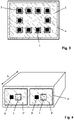
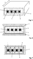
- FIG. 8 An embodiment of the invention is in figure 8 shown.
- the Figures 1 to 7 explain fiber optics in the optical arrangement of figure 8 can be used.
- figure 1 shows an optical waveguide in a sectional plan view. Viewed in cross-section, the optical waveguide has four different areas that consist of different materials with different optical properties. Each of the areas extends over the entire length of the optical waveguide.
- the Indian figure 1 The optical waveguide shown has four core regions 1 arranged next to one another. The core regions 1 are surrounded by a common first cladding 2, which has a lower refractive index than the core regions 1. The core regions 1 each have a region 3 doped with rare earth ions in their center. A second cladding 4, which in turn has a lower refractive index than the first cladding 2, encloses the arrangement of cores 1 and first cladding 2 and optically shields them from the outside.
- the length 5 of the optical waveguide is many times greater than the edge lengths of the square or rectangular core regions 1 and cladding regions 2 or 4.
- the length 5 of the optical waveguide is at least ten times the Rayleigh length of the light propagating in the optical waveguide.
- the core areas 1 consist of crystalline material, for example yttrium aluminum garnet.
- the cladding regions 2 and 4 are also preferably made of crystalline material. This however, is not a necessity.
- the jacket areas 2 and 4 can also consist of ceramic material or glass.
- the second jacket 4 is optional.
- the optical waveguide can have a cladding made of air.
- figure 1 shows a multi-core optical waveguide with a one-dimensional arrangement of the cores 1
- figure 2 a multi-core optical waveguide according to the invention is shown with a two-dimensional arrangement of the cores, seen in the cross section of the optical waveguide, in which the core regions are spaced apart from one another and arranged one above the other.
- the thermal coupling can be specifically influenced by the arrangement of the core areas 1 over the cross section of the optical waveguide.
- the two central core areas 1' are each surrounded by eight other cores.
- the core areas 1" arranged in the periphery are each surrounded by three or five other cores. This means that the probability of thermal interaction between the core areas 1', 1" is greater in the central core areas 1' than in the peripheral core areas 1". .
- the figure 3 shows a modified optical waveguide in which each core area 1 is surrounded by two further core areas, so that all core areas 1 have a similar thermal interaction with the other cores. This can improve the performance of the optical fiber.
- the threshold above which mode instability occurs can be raised further.
- the two first jacket areas 2 ′ are surrounded by a common second jacket area 4 .
- the doped region 3 is slightly outside of the core region 1. The arrangement of the doped region 3 relative to the light-guiding core region 1 and, if necessary, the overlapping of the doped region 3 with the core region 1 can be specifically selected in order to amplify individual modes of the in the optical waveguide to favor or suppress propagating light.
- the core areas 1 are formed by a plurality of channels 6 running along the longitudinal extension of the light waveguide, which, seen in the illustrated cross section of the light waveguide, are arranged around each core area 1, with the light waveguide in the areas forming the channels 6 having an opposite respective core region 1 or the cladding 2 has a lower refractive index.
- the optical waveguide Within the areas bounded by the channels 6, the optical waveguide has essentially the same refractive index as in the area of the first cladding 2.
- the channels 6 cause the light to be guided in the core areas 1.
- the channels 6 can be arranged in a targeted manner in order to influence the light guide and to to achieve a localization of a Gaussian basic mode in the core area and a simultaneous delocalization of higher-order modes, so that their propagation in the optical waveguide is suppressed as far as possible. With this strategy, the power threshold above which mode instability occurs can be further raised.
- the channels 6 can consist of crystalline or non-crystalline material, crystalline material being preferred here as well. It is possible to produce the channels 6 from material with low thermal conductivity (for example air), so that the channels 6 serve as a thermal and optical barrier between the core areas 1 at the same time. Also in the configuration with channels 6 to form the core areas 1, as in figure 5 shown, instead of the common first cladding 2, it can be provided that each core region 1 is assigned only one first cladding 2', similar to FIG figure 4 shown.
- the optical waveguide has, as mentioned, a rectangular cross section. This geometry is advantageous with regard to the production of the optical waveguide from crystalline materials.
- the rectangular cross-section has other advantages, such as from the figure 6 apparent.
- the optical waveguide shown is designed as in figure 1 shown. Plate-shaped cooling elements 7 are arranged on the upper and lower surfaces of the optical waveguide for heat dissipation. Due to the flat shape of the optical waveguide, the heat generated in the doped core areas 1 during the optical amplification can be dissipated particularly effectively. With regard to avoiding modal instability, it is advantageous that all core areas 1 are at the same distance from the cooling elements 7, so that uniform cooling is ensured.
- insulation areas 8 are arranged between the core areas 1, with the optical waveguide in the insulation areas 8 each having a reduced thermal conductivity compared to the other areas.
- the insulation areas serve to avoid thermal coupling between the core areas 1 in order to avoid mode instability.
- the isolation areas can be air or other suitable materials.
- the optical arrangement shown has a splitting element 9 which splits an input beam E into a plurality of spatially separate partial beams. These partial beams propagate through an optical waveguide 10, which is designed accordingly as a multi-core optical waveguide, as shown in FIGS Figures 1 to 7 shown. Each core area 1 of the optical waveguide guides a partial beam. Furthermore, a combination element 11 is provided, which spatially superimposes the partial beams in an output beam A.
- the splitting element 9 comprises two elements, namely a partially reflective element 12 and a reflective element 13.
- the reflective element 13 is a mirror with the highest possible reflectivity.
- the partially reflective element 12 reflects part of the incident radiation E (eg from a pulsed laser). The non-reflected part is transmitted and generates a partial beam.
- the input beam E is reflected back and forth multiple times between the partially reflective element 12 and the plane-parallel reflective element 13 arranged opposite thereto at a distance.
- the reflectivities of the zones of the partially reflective element 12 are selected in such a way that the incident input beam E is divided into the N partial beams in a specific ratio.
- the generated partial beams are parallel and equidistant.
- the combination element 11 has the same structure with a partially reflective element 12' and a reflective element 13'. The combination element 11 superimposes the partial beams in an output beam A.
Landscapes
- Physics & Mathematics (AREA)
- Electromagnetism (AREA)
- Optics & Photonics (AREA)
- Engineering & Computer Science (AREA)
- Plasma & Fusion (AREA)
- General Physics & Mathematics (AREA)
- Chemical & Material Sciences (AREA)
- Crystallography & Structural Chemistry (AREA)
- Microelectronics & Electronic Packaging (AREA)
- Lasers (AREA)
- Optical Integrated Circuits (AREA)
Description
- Die Erfindung betrifft eine optische Anordnung nach dem Oberbegriff des Anspruchs 1 sowie ein Verfahren zur Herstellung eines Lichtwellenleiters für eine solche optische Anordnung.
- Lichtwellenleiter (auch als "optische Fasern" bezeichnet) sind in verschiedenen Ausgestaltungen aus dem Stand der Technik bekannt. Lichtwellenleiter sind Leitungen zur Übertragung von Licht. Die bekannten Lichtwellenleiter sind dielektrische Wellenleiter, die aus konzentrischen Schichten aufgebaut sind. Im Zentrum liegt ein lichtführender Kern, der umschlossen ist von einem Mantel, der einen gegenüber dem Kern niedrigeren Brechungsindex aufweist. Bei kommerziellen Lichtwellenleitern sind außerdem den Mantel umgebende Schutzschichten aus Kunststoff vorgesehen. Je nach Anwendungsfall hat der Kern einen Durchmesser von einigen Mikrometern bis zu über einem Millimeter. Man unterscheidet Lichtwellenleiter unter anderem nach der Anzahl von ausbreitungsfähigen Moden der elektromagnetischen Strahlung des Lichts, die durch den Kerndurchmesser limitiert wird (Singlemode-/Multimodefasern).
- Die Weiterentwicklung von Faserlasern in jüngster Zeit hat dazu geführt, dass Lichtwellenleiter als aktives Medium ein zuverlässiges Konzept für Hochleistungslaser liefern. Die Entwicklung von Niedrigenergielasern zu Hochleistungslasern für industrielle Anwendungen basiert auf der Fähigkeit von Lichtwellenleitern, hohe Leistung handhaben zu können. Das sehr gute Verhältnis von Oberfläche zu aktivem Volumen erlaubt es, Wärme effizient abzuführen. Dies ist eine hervorragende Voraussetzung für einen Hochleistungsbetrieb. Allerdings führen Bedingungen im Lichtwellenleiter zu anderen Problemen. So führt beispielsweise die Einschränkung des Lichtsignals auf den Kern des Lichtwellenleiters zu hoher Lichtintensität und zu Wechselwirkungen zwischen dem Material des Lichtwellenleiters und dem Lichtsignal. Dabei entstehen insbesondere auch schwer zu kontrollierende nichtlineare Effekte. Damit wird die Signalqualität stark beeinträchtigt.
- Lichtwellenleiter sollten demnach derart ausgelegt werden, dass nichtlineare Effekte und Wechselwirkungen mit dem Fasermaterial reduziert werden. Am einfachsten und effektivsten werden nichtlineare Effekte durch ein Vergrößern des Durchmessers des Kerns reduziert. Dadurch wird zum einen die Intensität des Lichts im Kern reduziert und zum anderen kann, beispielsweise bei doppelmanteligen Lichtwellenleitern, die Absorption von Pumplicht erhöht werden. Aufgrund der verbesserten Absorption des Pumplichts kann der Lichtwellenleiter verkürzt werden und damit können nichtlineare Effekte weiter reduziert werden.
- Bei einem großen Kerndurchmesser des Lichtwellenleiters ist es allerdings schwierig, einen Singlemode-Betrieb oder auch einen Betrieb mit nur wenigen Moden umzusetzen, insbesondere im Hochleistungsbetrieb. Hierzu müssen zusätzliche Maßnahmen ergriffen werden, vor allem bei einer hohen thermischen Belastung.
- Es hat sich allerdings gezeigt, dass die bisher bekannten Maßnahmen zur Optimierung von Lichtwellenleitern für den Hochleistungsbetrieb nicht zuverlässig verhindern können, dass es zu Modeninstabilität bei hohen Leistungen kommt. Dabei wird das Ausgangsignal des Lichtwellenleiters oder eines damit realisierten Faserlasers instabil, sobald eine bestimmte Leistungsschwelle überschritten wird. Es wird Energie von einer Grundmode in Moden höherer Ordnung übertragen. Das z.B. ursprünglich stabil Gauß-förmige Strahlprofil der im Lichtwellenleiter propagierenden Strahlung beginnt sich zu verändern und das Strahlprofil fluktuiert zeitlich aufgrund einer zeitlich veränderlichen Überlagerung der Grundmode mit einer oder mehreren Moden höherer Ordnung. Das Zeitverhalten dieser Fluktuationen kann deterministisch oder, je nach Leistung der propagierenden Strahlung, auch zufällig oder chaotisch sein. Dabei ist es bekannt, dass die Modeninstabilität auf räumlichen Temperaturvariationen innerhalb des Lichtwellenleiters aufgrund der Modeninterferenz basiert. Diese bewirkt eine räumlich und zeitlich veränderliche Strahlungsabsorption im Material des Lichtwellenleiters. Aufgrund thermooptischer Effekte wirkt sich dies unmittelbar auf die Lichtführung aus. Durch das sich aufgrund der Modeninterferenz einstellende räumliche Temperaturprofil des Lichtwellenleiters entsteht eine Gitterstruktur des Brechungsindexprofils, die einen Energietransfer zwischen den verschiedenen Moden der propagierenden Strahlung begünstigt.
- Mu et al. ("Double clad YAG crystalline fiber waveguides for diode pumped high power lasing", Proc. of SPIE, Bd. 8959, 28. Februar 2014, S. 895906-1 / 895906-9) beschreiben einen kristallinen Doppelmantel-Lichtwellenleiter (CFW). Dieser besteht aus einem Yb:YAG-Kern, einem undotierten YAG-Innenmantel und einem keramischem Spinell-Außenmantel. Der Lichtwellenleiter kommt in einem Master-Oszillator-Verstärker-(MOPA)-Experiment zum Einsatz.
- Mu et al. ("True crystalline fibers: double-clad LMA design concept of Tm:YAG-core fiber and its mode simulation", FIBER LASERS IX: TECHNOLOGY, SYSTEMS, AND APPLICATIONS, SPIE, Bd. 8237, Nr. 1, 8. März 2012, Seiten 1-5) beschreiben des Weiteren einen doppelt ummantelten Lichtwellenleiter mit einem einkristallinen, rechteckigen Kern aus Tm:YAG als Verstärkungsmedium für einen LMA-Faserlaser. Der Lichtwellenleiter verwendet undotierten YAG und keramischen Spinell für die Innen- bzw. Außenbeschichtung. Die Struktur weist eine große numerische Apertur für den undotierten YAG-Innenmantel auf, der zum optischen Pumpen zur Verfügung steht.
- Die
US 2013/235448 A1 offenbart eine optische Verstärkeranordnung zur Verstärkung ultrakurzer gepulster Laserstrahlung. Die Anordnung umfasst einen modengekoppelten Laser und zwei oder mehr in Propagationsrichtung nach dem Laser angeordneten optischen Verstärkern. Zwischen dem Laser und den optischen Verstärkern befindet sich mindestens ein Aufteilungselement, welches die gepulste Laserstrahlung auf mehrere Verstärkerkanäle aufteilt. Den Verstärkerkanälen ist mindestens ein gemeinsames Kombinationselement nachgeordnet ist, welches die in den Verstärkerkanälen verstärkte gepulste Laserstrahlung kohärent überlagert. - Die
WO 2014/087468 A1 offenbart einen Lichtwellenleiter, bei dem ein transparentes Element und ein Lasermedium zwischen einem ersten Mantel und einem zweiten Mantel sandwichartig angeordnet sind. Pumplicht wird aus einer Richtung senkrecht zu den optischen Achsen der erzeugten Laserstrahlung einfallen gelassen und breitet sich abwechselnd durch das transparente Element und das zickzackförmige Lasermedium aus. - Vor diesem Hintergrund ist es Aufgabe der Erfindung, eine optische Anordnung mit einem Lichtwellenleiter für den Hochleistungsbetrieb bereitzustellen, die hinsichtlich Modeninstabilität gegenüber dem Stand der Technik verbessert ist.
- Diese Aufgabe löst die Erfindung durch eine optische Anordnung mit den Merkmalen des Anspruchs 1.
- Die Erfindung betrifft eine optische Anordnung mit
- einem Aufteilungselement, das einen Eingangsstrahl in mindestens zwei Teilstrahlen aufteilt,
- wenigstens einem Mehrkern-Lichtwellenleiter, durch den die Teilstrahlen propagieren, wobei jeder Kernbereich jeweils einen Teilstrahl führt, und
- wenigstens einem Kombinationselement, das die Teilstrahlen in einem Ausgangsstrahl räumlich überlagert.
- Die Erfindung basiert auf dem Ansatz, das Auftreten von Modeninstabilität zu vermeiden bzw. die Leistungsschwelle, ab der Modeninstabilität auftritt, zu höheren Werten hin zu verschieben, indem im Lichtwellenleiter für die Lichtführung ein Material mit gegenüber dem Stand der Technik verbesserten thermischen und thermooptischen Eigenschaften verwendet wird. Kristalline Materialien, wie Yttrium-Aluminium-Granat, Saphir oder Diamant sind bekannt für ihre exzellenten thermischen Eigenschaften, die um wenigstens eine Größenordnung besser sind als die Eigenschaften von Quarzglas, aus denen herkömmliche Lichtwellenleiter zumeist bestehen. Allein durch den Einsatz von kristallinem Material im Kernbereich des Lichtwellenleiters wird die Schwelle, ab der Modeninstabilität auftritt, signifikant angehoben. Entsprechend kann die durchschnittliche Ausgangsleistung eines Lasers, der mit einem Lichtwellenleiter als aktives Medium arbeitet, deutlich gegenüber dem Stand der Technik erhöht werden.
- Kristalline Materialien, insbesondere Yttrium-Aluminium-Granat, sind als aktive Medien in Festkörperlasern aus dem Stand der Technik bekannt. Mit Nd:YAG- oder Yb:YAG-Lasern lässt sich Laserstrahlung mit einer Leistung von über 1000 W erzeugen. Zwar lassen sich mit bekannten Faserlasern bereits heute noch höhere Leistungen erzeugen. Dies belegt allerdings nur das Potenzial von Faserlasern, wenn in diesen kristallines Material in den lichtführenden Bereichen eingesetzt wird, da die bekannten Faserlaser-Konzepte herkömmliche Lichtwellenleiter auf Basis von Quarzglas vorsehen, die den genannten kristallinen Materialien hinsichtlich der thermischen und thermooptischen Eigenschaften, wie erwähnt, deutlich unterlegen sind.
- Bei einer möglichen Ausgestaltung des Lichtwellenleiters weist dieser in dem den ersten Mantel bildenden Bereich einen niedrigeren Brechungsindex auf als im Kernbereich. Dies entspricht dem herkömmlichen Design von Lichtwellenleitern.
- Alternativ kann der Kernbereich durch eine Mehrzahl von entlang der Längserstreckung des Lichtwellenleiters verlaufenden Kanälen gebildet sein, die, im Querschnitt des Lichtwellenleiters gesehen, um den Kernbereich herum angeordnet sind, wobei der Lichtwellenleiter in den die Kanäle bildenden Bereichen einen gegenüber dem jeweiligen Kernbereich niedrigeren Brechungsindex aufweist. Die den Kernbereich umgrenzenden Kanäle bewirken bei dieser Ausgestaltung die Lichtführung im Kernbereich.
- Für den Einsatz des Lichtwellenleiters als optischer Verstärker, beispielsweise in einem Faserlaser, weist der Lichtwellenleiter, im Querschnitt gesehen, zumindest einen mit Seltenerdionen dotierten Bereich auf, der zumindest teilweise mit dem Kernbereich überlappt. In Kombination mit einem geeigneten Pumplicht, das neben der eigentlichen Nutzstrahlung im Lichtwellenleiter propagiert, bewirkt die Dotierung stimulierte Emission und damit Verstärkung der Nutzstrahlung.
- Bei einer weiter bevorzugten Ausgestaltung des Lichtwellenleiters ist ein zweiter Mantel vorgesehen, der, im Querschnitt des Lichtwellenleiters gesehen, den ersten Mantel umschließt, wobei der Lichtwellenleiter in dem den zweiten Mantel bildenden Bereich einen niedrigeren Brechungsindex aufweist als im Bereich des ersten Mantels. Auf diese Weise entsteht eine Doppelmantelstruktur. Der zweite Mantel schirmt die Anordnung aus Kern und erstem Mantel gegenüber der Umgebung optisch ab. Der erste Mantel kann für die Propagation von Pumplicht in dem Lichtwellenleiter dienen. Die unterschiedlichen Brechungsindizes des ersten und zweiten Mantels bewirken dabei die Führung des Pumplichts in dem Lichtwellenleiter.
- Bei einer besonders bevorzugten Ausgestaltung besteht der Lichtwellenleiter nicht nur im Kernbereich aus kristallinem Material, sondern auch im Bereich des ersten und/oder zweiten Mantels, um deren thermische und thermooptische Eigenschaften ebenfalls zu optimieren. Alternativ können der erste und/oder der zweite Mantel aus keramischem Material oder auch aus Glas, beispielsweise Quarzglas bestehen.
- Bevorzugt weisen der Kernbereich und der erste und/oder der zweite Mantel des Lichtwellenleiters jeweils einen rechteckigen oder quadratischen Querschnitt auf, wobei die Kantenlängen kleiner sind als die Länge des Lichtwellenleiters. Die Länge des Lichtwellenleiters sollte zumindest das Zehnfache der Rayleigh-Länge des in dem Lichtwellenleiter propagierenden Lichts betragen. Herkömmliche Lichtwellenleiter weisen typischerweise einen kreisrunden oder elliptischen Querschnitt auf. Dies resultiert jedoch im Wesentlichen aus dem Herstellungsprozess, der bei herkömmlichen Lichtwellenleitern eingesetzt wird. Die runde Form ist kein optisches Erfordernis. Lichtwellenleiter mit kristallinem Kern und gegebenenfalls auch kristallinem Mantel lassen sich, wie weiter unten noch ausgeführt wird, besser mit einer im Querschnitt rechteckigen Form herstellen. In Bezug auf die Lichtführung bedeutet dies keinen Nachteil. Tatsächlich hat die rechteckige Form sogar Vorteile im Hinblick auf die Wärmeableitung, insbesondere bei mehrere Kerne aufweisenden Lichtwellenleitern, worauf weiter unten noch eingegangen wird.
- Ein besonders vielversprechendes Konzept zur Anhebung der Schwelle von Modeninstabilität ist der Einsatz von Mehrkern-Lichtwellenleitern, das heißt Lichtwellenleitern, die nebeneinander mehrere unabhängige aktive, d.h. geeignet dotierte Kernbereiche aufweisen. Es zeigt sich, dass die Leistungsschwelle, ab der Modeninstabilität auftritt, in etwa mit der Zahl der Kerne in einem Mehrkern-Lichtwellenleiter skaliert. Dem Konzept liegt zugrunde, dass der zu verstärkende Lichtstrahl vor der Einkopplung in den Lichtwellenleiter in Teilstrahlen aufgeteilt wird, wobei jeder der Kernbereiche des Mehrkern-Lichtwellenleiters jeweils einen Teilstrahl führt. Nach Durchlaufen des Lichtwellenleiters werden die Teilstrahlen wieder in einem einzelnen Ausgangsstrahl überlagert. Erfindungsgemäß ist entsprechend vorgesehen, dass der Lichtwellenleiter eine Mehrzahl von Kernbereichen aufweist, die, im Querschnitt des Lichtwellenleiters gesehen, voneinander beabstandet neben- und/oder übereinander angeordnet sind. Auf diese Weise entsteht ein mehrkerniger kristalliner Lichtwellenleiter, bei dem die erzielbare Ausgangsleistung gegenüber dem Stand der Technik angehoben ist. Dabei hat die Anordnung mehrerer Kerne in einer gemeinsamen Lichtwellenleiterstruktur den Vorteil, dass alle Licht führenden Kernbereiche identischen Umgebungseinflüssen (zum Beispiel identischen Temperaturschwankungen) ausgesetzt sind. Das bedeutet, dass keine signifikanten relativen Schwankungen der optischen Weglängen der Teilstrahlen in dem Lichtwellenleiter auftreten, was zu Störungen bei der Vereinigung der Teilstrahlen im Ausgangsstrahl führen würde.
- Bei einer bevorzugten Ausgestaltung des Mehrkern- Lichtwellenleiters sind die Kernbereiche von einem gemeinsamen ersten Mantel umgeben, ebenso kann jeder Kernbereich von einem jeweils nur diesem Kernbereich zugeordneten ersten Mantel umgeben sein, um die einzelnen Kerne besser voneinander abzuschirmen.
- Bei einer weiter bevorzugten Ausgestaltung des Lichtwellenleiters ist ein Isolationsbereich vorgesehen, der, im Querschnitt des Lichtwellenleiters gesehen, zwischen wenigstens zwei Kernbereichen angeordnet ist, wobei der Lichtwellenleiter im Isolationsbereich eine gegenüber den übrigen Bereichen reduzierte Wärmeleitfähigkeit aufweist. Auf diese Weise wird verhindert, dass eine thermische Wechselwirkung zwischen den verschiedenen Kernbereichen des Mehrkern-Lichtwellenleiters auftritt. Zumindest wird eine entsprechende Wechselwirkung reduziert. Eine solche thermische Wechselwirkung könnte wiederum zu einer Herabsetzung der Leistungsschwelle, ab der Modeninstabilität auftritt, führen. Zur Vermeidung der gegenseitigen thermischen Beeinflussung der Kernbereiche können diese in der den ersten Mantel bildenden Matrix der Lichtwellenleiterstruktur geometrisch optimiert angeordnet sein, um thermische Wechselwirkungen zu minimieren bzw. eine wechselseitig möglichst symmetrische thermische Wechselwirkung zwischen den Kernbereichen zu erzielen.
- Besonders bevorzugt weisen das Aufteilungselement und/oder das Kombinationselement jeweils ein teilreflektives Element auf, das die Strahlung des Eingangsstrahls bzw. des Ausgangsstrahls zwei- oder mehrfach reflektiert, wobei das teilreflektive Element Zonen unterschiedlicher Reflektivität aufweist.
- Es erfolgt eine Aufteilung des Eingangsstrahls in mehrere Teilstrahlen, so dass mehrere möglichst unabhängige Kanäle für die propagierende Strahlung verwendet werden. In der optischen Anordnung fungiert der Lichtwellenleiter als Multikanalelement, durch das die Teilstrahlen räumlich voneinander getrennt propagieren. Zur optischen Verstärkung kann die Führung der Pumpstrahlung in dem Lichtwellenleiter in mehreren getrennten Mantelbereichen als Pumpkanälen oder in einem gemeinsamen Mantelbereich als Pumpkanal erfolgen.
- Die erfindungsgemäße optische Anordnung weist bevorzugt ein kompaktes und winkeldispersionsfreies Aufteilungs- und Kombinationselement zur Aufteilung bzw. Kombination der Strahlung auf. Das Aufteilungselement und das Kombinationselement sind bevorzugt identisch ausgebildet, so dass die Aufteilung und die Kombination der Strahlung symmetrisch erfolgen. Erfindungsgemäß weisen das Aufteilungselement und/oder das Kombinationselement bevorzugt jeweils ein teilreflektives Element auf, das die Strahlung des Eingangsstrahls bzw. des Ausgangsstrahls zwei- oder mehrfach reflektiert, wobei das teilreflektive Element Zonen unterschiedlicher Reflektivität aufweist. Die Strahlung des Eingangsstrahls bzw. des Ausgangsstrahls wird, mit anderen Worten, nacheinander an den verschiedenen Zonen des teilreflektiven Elementes, d.h. bei jedem Teilreflektionsvorgang mit einer anderen Reflektivität, reflektiert. Dabei wird z.B. die Reflektivität der Zonen des teilreflektiven Elementes entlang einer in der Reflektionsebene der Strahlung liegenden Richtung kleiner bzw. größer, je nachdem ob es sich um das Aufteilungs- oder das Kombinationselement handelt. Die unterschiedliche (abnehmende bzw. ansteigende) Reflektivität bewirkt, dass, z.B. im Aufteilungselement, jeder Teilstrahl, der bei einem der nacheinander erfolgenden Teilreflektionsvorgänge als nicht reflektierter Anteil des Eingangsstrahls erzeugt wird, eine bestimmte, vorzugsweise gleiche Intensität erhält.
- Zweckmäßig weisen das Aufteilungselement und/oder das Kombinationselement weiterhin jeweils ein reflektives Element auf, wobei die Strahlung dann zwischen teilreflektivem und reflektivem Element mehrfach hin und her reflektiert wird. Dabei kann die Oberfläche des reflektiven Elementes planparallel zu der Oberfläche des teilreflektiven Elementes sein. Zweckmäßig fällt die Strahlung schräg, d.h. unter einem von 90° abweichenden Winkel auf das teilreflektive Element ein, so dass die Teilstrahlen nach der Aufteilung in einer gemeinsamen Ebene, parallel und mit äquidistantem Abstand propagieren. Dabei ist der Einfallswinkel so zu wählen, dass die Strahlung nacheinander an den Zonen unterschiedlicher Reflektivität teilreflektiert wird.
- Der Lichtwellenleiter kann auf verschiedene Art und Weise hergestellt werden.
- Ein mögliches Herstellungsverfahren weist die folgenden Verfahrensschritte auf:
- Einbringen wenigstens einer Vertiefung in ein erstes Substratstück,
- epitaktisches Aufwachsen eines den Kernbereich bildenden kristallinen Materials auf dem ersten Substratstück,
- Entfernen des kristallinen Materials von der Oberfläche des ersten Substratstücks, so dass das kristalline Material nur im Bereich der Vertiefung verbleibt, und
- Aufbringen eines zweiten Substratstücks auf die Oberfläche des ersten Substratstücks und Verbinden der beiden Substratstücke, so dass diese gemeinsam den ersten Mantel bilden.
- Als Substrat wird bei diesem Herstellungsverfahren dasjenige Material des Lichtwellenleiters verwendet, das im fertigen Lichtwellenleiter den ersten Mantel bildet. In das Substrat wird zunächst, zum Beispiel durch chemisches Ätzen, eine Vertiefung in Richtung der Längserstreckung des Lichtwellenleiters eingebracht. Zur Herstellung eines Mehrkern-Lichtwellenleiters werden nebeneinander mehrere Vertiefungen in das erste Substratstück eingebracht. Die Vertiefung wird dann mit dem dotierten Material ausgefüllt, das in dem fertigen Lichtwellenleiter den Kernbereich bildet. Zur Erzeugung des kristallinen Kerns wird das Material epitaktisch auf dem ersten Substratstück aufgewachsen. Im nächsten Schritt wird das kristalline Material, zum Beispiel durch Schleifen oder Polieren, wieder von der Oberfläche des ersten Substratstücks entfernt, so dass das kristalline Material des Kerns nur im Bereich der Vertiefung bzw. der Vertiefungen verbleibt. Ein zweites Substratstück, das gemeinsam mit dem ersten Substratstück den ersten Mantel des Lichtwellenleiters bildet, wird dann auf das erste Substratstück aufgebracht und mit diesem, ohne oder mit einem geeigneten Adhäsiv, verbunden. Gegebenenfalls kann der so erzeugte Lichtwellenleiter an seinen äußeren Oberflächen mit weiterem Material bedeckt werden, das den zweiten Mantel des Lichtwellenleiters bildet.
- Ein Ausführungsbeispiel der Erfindung wird in
Figur 8 dargestellt. DieFiguren 1 bis 7 erläutern Lichtwellenleiter die in der optischen Anordnung derFigur 8 eingesetzt werden können. - Es zeigen:
- Figur 1:
- geschnittene Draufsicht eines Lichtwellenleiters mit mehreren nebeneinander angeordneten Kernen;
- Figur 2:
- Querschnittdarstellung eines Lichtwellenleiters mit neben- und übereinander angeordneten Kernen;
- Figur 3:
- Querschnittdarstellung eines Lichtwellenleiters mit optimierter Anordnung der Kernbereiche;
- Figur 4:
- geschnittene Draufsicht eines Lichtwellenleiters mit außerhalb der Kerne angeordneter Dotierung;
- Figur 5:
- geschnittene Draufsicht eines Lichtwellenleiters mit von Kanälen umgrenzten Kernbereichen;
- Figur 6:
- Querschnittdarstellung eines Lichtwellenleiters mit Kühlelementen;
- Figur 7:
- Querschnittdarstellung eines Lichtwellenleiters mit thermischen Isolationsbereichen zwischen den Kernbereichen;
- Figur 8:
- schematische Darstellung einer optischen Anordnung mit Lichtwellenleiter.
-
Figur 1 zeigt einen Lichtwellenleiter in einer geschnittenen Draufsicht. Im Querschnitt gesehen weist der Lichtwellenleiter vier verschiedene Bereiche auf, die aus unterschiedlichen Materialien mit unterschiedlichen optischen Eigenschaften bestehen. Jeder der Bereiche erstreckt sich jeweils über die gesamte Längserstreckung des Lichtwellenleiters. Der in derFigur 1 dargestellte Lichtwellenleiter weist vier nebeneinander angeordnete Kernbereiche 1 auf. Die Kernbereiche 1 sind von einem gemeinsamen ersten Mantel 2 umgeben, der einen niedrigeren Brechungsindex aufweist als die Kernbereiche 1. Die Kernbereiche 1 weisen in ihrem Zentrum jeweils einen mit Seltenerdionen dotierten Bereich 3 auf. Ein zweiter Mantel 4, der seinerseits einen niedrigeren Brechungsindex aufweist als der erste Mantel 2, umschließt die Anordnung aus Kernen 1 und erstem Mantel 2 und schirmt diese nach außen optisch ab. Die Länge 5 des Lichtwellenleiters ist um ein Vielfaches größer als die Kantenlängen der quadratisch bzw. rechteckig ausgebildeten Kernbereiche 1 und Mantelbereiche 2 bzw. 4. Die Länge 5 des Lichtwellenleiters beträgt zumindest das Zehnfache der Rayleigh-Länge des in dem Lichtwellenleiter propagierenden Lichts. Erfindungsgemäß bestehen die Kernbereiche 1 aus kristallinem Material, beispielsweise aus Yttrium-Aluminium-Granat. Auch die Mantelbereiche 2 und 4 bestehen vorzugsweise aus kristallinem Material. Dies ist allerdings keine Notwendigkeit. Die Mantelbereiche 2 und 4 können ebenso aus keramischem Material oder aus Glas bestehen. Der zweite Mantel 4 ist optional. Der Lichtwellenleiter kann alternativ einen Mantel aus Luft aufweisen. Während dieFigur 1 einen Mehrkern-Lichtwellenleiter mit einer eindimensionalen Anordnung der Kerne 1 zeigt, ist inFigur 2 ein Mehrkern-Lichtwellenleiter gemäß der Erfindung mit einer, im Querschnitt des Lichtwellenleiters gesehen, zweidimensionalen Anordnung der Kerne gezeigt, in der die Kernbereiche voneinander beabstandet neben- und übereinander angeordnet sind. - Bei den in den
Figuren 1 und 2 dargestellten Lichtwellenleitern sind keine besonderen Maßnahmen getroffen, die Kernbereiche 1 thermisch voneinander abzuschirmen. Die thermischen Einflussbereiche der Kerne 1 erstrecken sich deutlich über die dotierten Bereiche 3 hinaus, so dass eine thermische Kopplung zwischen den verschiedenen Kernbereichen 1 nicht auszuschließen ist. Die thermische Kopplung kann durch die Anordnung der Kernbereiche 1 über den Querschnitt des Lichtwellenleiters gezielt beeinflusst werden. Beispielsweise bei der Anordnung in derFigur 2 sind die beiden zentralen Kernbereiche 1' jeweils von acht anderen Kernen umgeben. Die in der Peripherie angeordneten Kernbereiche 1" sind jeweils von drei oder von fünf anderen Kernen umgeben. Das bedeutet, dass die Wahrscheinlichkeit thermischer Wechselwirkung zwischen den Kernbereichen 1', 1" bei den zentralen Kernbereichen 1' größer ist als bei den peripheren Kernbereichen 1". - Die
Figur 3 zeigt einen modifizierten Lichtwellenleitern, bei dem jeder Kernbereich 1 von zwei weiteren Kernbereichen umgeben ist, so dass alle Kernbereiche 1 eine ähnliche thermische Wechselwirkung mit den anderen Kernen aufweisen. Dadurch kann die Leistung des Lichtwellenleiters verbessert werden. Insbesondere kann die Schwelle, ab der Modeninstabilität auftritt, weiter angehoben werden. - Bei den Lichtwellenleitern der
Figuren 1-3 sind alle Kernbereiche 1 von einem gemeinsamen ersten Mantelbereich 2 umgeben. Bei dem in derFigur 4 dargestellten Ausführungsbeispiel ist jeder Kernbereich 1 von einem jeweils nur diesem Kernbereich zugeordneten ersten Mantel 2' geben, um die einzelnen Kanäle des Mehrkern-Lichtwellenleiters besser voneinander abzuschirmen. Die beiden ersten Mantelbereiche 2' sind von einem gemeinsamen zweiten Mantelbereich 4 umgeben. Außerdem liegt bei dem in derFigur 4 dargestellten Ausführungsbeispiel der dotierte Bereich 3 etwas außerhalb des Kernbereichs 1. Die Anordnung des dotierten Bereichs 3 relativ zu dem lichtführenden Kernbereich 1 und gegebenenfalls die Überlappung des dotierten Bereichs 3 mit dem Kernbereich 1 kann gezielt gewählt werden, um die Verstärkung einzelner Moden des in dem Lichtwellenleiter propagierenden Lichts zu begünstigen bzw. zu unterdrücken. - Bei dem in der
Figur 5 gezeigten Lichtwellenleitern werden die Kernbereiche 1 durch eine Mehrzahl von entlang der Längserstreckung des Lichtwellenleiters verlaufenden Kanälen 6 gebildet, die, im dargestellten Querschnitt des Lichtwellenleiters gesehen, um jeden Kernbereich 1 herum angeordnet sind, wobei der Lichtwellenleiter in den die Kanäle 6 bildenden Bereichen einen gegenüber dem jeweiligen Kernbereich 1 bzw. dem Mantel 2 niedrigeren Brechungsindex aufweist. Innerhalb der von den Kanälen 6 umgrenzten Bereiche weist der Lichtwellenleiter im Wesentlichen denselben Brechungsindex auf wie im Bereich des ersten Mantels 2. Die Kanäle 6 bewirken die Lichtführung in den Kernbereichen 1. Die Kanäle 6 können gezielt angeordnet werden, um die Lichtführung zu beeinflussen und um eine Lokalisierung einer Gauß-artigen Grundmode im Kernbereich und eine gleichzeitige Delokalisierung von Moden höherer Ordnung zu erreichen, damit deren Propagation in dem Lichtwellenleiter möglichst unterdrückt wird. Durch diese Strategie kann die Leistungsschwelle, ab der Modeninstabilität auftritt, weiter angehoben werden. Die Kanäle 6 können aus kristallinem oder nicht-kristallinem Material bestehen, wobei auch hier kristallines Material bevorzugt wird. Möglich ist es, die Kanäle 6 aus Material mit geringer Wärmeleitfähigkeit (zum Beispiel Luft) herzustellen, so dass die Kanäle 6 gleichzeitig als thermische und optische Barriere zwischen den Kernbereichen 1 dienen. Auch bei der Ausgestaltung mit Kanälen 6 zur Bildung der Kernbereiche 1, wie inFigur 5 dargestellt, kann statt des gemeinsamen ersten Mantels 2 vorgesehen sein, dass jedem Kernbereich 1 jeweils nur ein erster Mantel 2' zugeordnet ist, ähnlich wie inFigur 4 dargestellt. - Bei sämtlichen der in den Figuren dargestellten Anordnungen weist der Lichtwellenleiter, wie erwähnt, einen rechteckigen Querschnitt auf. Diese Geometrie ist im Hinblick auf die Herstellung des Lichtwellenleiters aus kristallinen Materialien vorteilhaft. Der rechteckige Querschnitt hat weitere Vorteile, wie zum Beispiel aus der
Figur 6 ersichtlich. Der dargestellte Lichtwellenleiter ist ausgebildet wie inFigur 1 dargestellt. Zur Wärmeabfuhr sind an den oberen und unteren Flächen des Lichtwellenleiters plattenförmige Kühlelemente 7 angeordnet. Aufgrund der flachen Form des Lichtwellenleiters kann die in den dotierten Kernbereichen 1 bei der optischen Verstärkung anfallende Wärme besonders effektiv abgeführt werden. Im Hinblick auf die Vermeidung von Modeninstabilität ist dabei von Vorteil, dass alle Kernbereiche 1 von den Kühlelementen 7 denselben Abstand haben, so dass für eine gleichmäßige Kühlung gesorgt ist. - Bei dem in
Figur 7 dargestellten Lichtwellenleitern sind Isolationsbereiche 8 zwischen den Kernbereichen 1 angeordnet, wobei der Lichtwellenleiter in den Isolationsbereichen 8 jeweils eine gegenüber den übrigen Bereichen reduzierte Wärmeleitfähigkeit aufweist. Die Isolationsbereiche dienen zur Vermeidung thermischer Kopplung zwischen den Kernbereichen 1, um Modeninstabilität zu vermeiden. Die Isolationsbereiche können aus Luft oder aus anderen geeigneten Materialien bestehen. - Die in der
Figur 8 dargestellte optische Anordnung weist ein Aufteilungselement 9 auf, das einen Eingangsstrahl E in mehrere räumlich separate Teilstrahlen aufteilt. Diese Teilstrahlen propagieren durch einen Lichtwellenleiter 10, der entsprechend als Mehrkern-Lichtwellenleiter ausgebildet ist, wie in denFiguren 1 bis 7 dargestellt. Jeder Kernbereich 1 des Lichtwellenleiters führt dabei jeweils einen Teilstrahl. Des Weiteren ist ein Kombinationselement 11 vorgesehen, das die Teilstrahlen in einem Ausgangsstrahl A räumlich überlagert. Das Aufteilungselement 9 umfasst zwei Elemente, nämlich ein teilreflektives Element 12 und ein reflektives Element 13. Bei dem reflektiven Element 13 handelt es sich um einen Spiegel mit möglichst hoher Reflektivität. Das teilreflektive Element 12 reflektiert einen Teil der (z.B. von einem Pulslaser) einfallenden Strahlung E. Der nicht reflektierte Teil wird transmittiert und erzeugt einen Teilstrahl. Das teilreflektive Element 12 besteht aus N (in dem dargestellten Ausführungsbeispiel gilt N=4) Zonen mit unterschiedlicher Reflektivität. Der Eingangsstrahl E wird zwischen dem teilreflektiven Element 12 und dem dazu gegenüberliegend mit Abstand angeordneten, planparallelen reflektiven Element 13 mehrfach hin und her reflektiert. Die Reflektivitäten der Zonen des teilreflektiven Elementes 12 sind so gewählt, dass der einfallende Eingangsstrahl E in einem bestimmten Verhältnis auf die N Teilstrahlen aufgeteilt wird. Die erzeugten Teilstrahlen sind hierbei parallel und äquidistant. Das Kombinationselement 11 hat einen gleichen Aufbau mit teilreflektivem Element 12' und reflektivem Element 13'. Das Kombinationselement 11 überlagert die Teilstrahlen in einem Ausgangsstrahl A. Dabei ist es in der Weise antisymmetrisch zu dem Aufteilungselement 1 angeordnet, dass sich die entstehenden Weglängenunterschiede der N Teilstrahlen genau aufheben. Aufgrund der Integration der 1:N-Teilung bzw. -Kombination in jeweils einem einzelnen Element 9 bzw. 11 ist eine kompakte Bauweise möglich, und es wird eine einfache Justage gewährleistet.
Claims (15)
- Optische Anordnung mit- einem Aufteilungselement (9), das einen Eingangsstrahl (E) in mindestens zwei räumlich getrennte Teilstrahlen aufteilt,- wenigstens einem Lichtwellenleiter (10), durch den die Teilstrahlen propagieren, und- wenigstens einem Kombinationselement (11), das die Teilstrahlen in einem Ausgangsstrahl (A) räumlich überlagert,dadurch gekennzeichnet,
dass der Lichtwellenleiter (10) eine Mehrzahl von entlang der Längserstreckung des Lichtwellenleiters (10) verlaufenden Kernbereichen (1) aufweist, die, im Querschnitt des Lichtwellenleiters gesehen, voneinander beabstandet neben- und/oder übereinander angeordnet sind, und einen ersten Mantel (2), der, im Querschnitt des Lichtwellenleiters gesehen, die Kernbereiche (1) umschließt, wobei der Lichtwellenleiter (10) wenigstens in den Kernbereichen (1) aus kristallinem Material besteht, wobei jeder Kernbereich (1) jeweils einen Teilstrahl führt, wobei der Mantel (2) aus einem einheitlichen, undotierten Material besteht, wobei der Lichtwellenleiter (10), im Querschnitt gesehen, mit Seltenerdionen dotierte Bereiche (3) aufweist, die zumindest teilweise mit den Kernbereichen (1) überlappen. - Optische Anordnung nach Anspruch 1, dadurch gekennzeichnet, dass der Lichtwellenleiter (10) in dem den ersten Mantel bildenden Bereich (2) einen niedrigeren Brechungsindex aufweist als in den Kernbereichen (1).
- Optische Anordnung nach Anspruch 1, dadurch gekennzeichnet, dass die Kernbereiche (1) jeweils durch eine Mehrzahl von entlang der Längserstreckung des Lichtwellenleiters (10) verlaufende Kanäle (6) gebildet werden, die, im Querschnitt des Lichtwellenleiters gesehen, um die Kernbereiche (1) herum angeordnet sind, wobei der Lichtwellenleiter (10) in den die Kanäle (6) bildenden Bereichen einen gegenüber dem Kernbereich (1) niedrigeren Brechungsindex aufweist.
- Optische Anordnung nach einem der Ansprüche 1 bis 3, dadurch gekennzeichnet, dass das kristalline Material Yttrium-Aluminium-Granat, Saphir oder Diamant ist.
- Optische Anordnung nach einem der Ansprüche 1 bis 4, gekennzeichnet durch einen zweiten Mantel (4), der, im Querschnitt des Lichtwellenleiters gesehen, den ersten Mantel (2) umschließt, wobei der Lichtwellenleiter in dem den zweiten Mantel bildenden Bereich (4) einen niedrigeren Brechungsindex aufweist als im Bereich des ersten Mantels (2).
- Optische Anordnung nach einem der Ansprüche 1 bis 5, dadurch gekennzeichnet, dass der Lichtwellenleiter im Bereich des ersten und/oder zweiten Mantels (2, 4) aus einem kristallinen oder keramischen Material oder aus einem Glas besteht.
- Optische Anordnung nach einem der Ansprüche 1 bis 6, dadurch gekennzeichnet, dass die Kernbereiche (1) und der erste und/oder der zweite Mantel (2, 4) jeweils einen rechteckigen oder quadratischen Querschnitt aufweisen.
- Optische Anordnung nach Anspruch 7, dadurch gekennzeichnet, dass der Lichtwellenleiter (10) insgesamt einen rechteckigen oder quadratischen Querschnitt aufweist.
- Optische Anordnung nach einem der Ansprüche 1 bis 8, dadurch gekennzeichnet, dass die Kernbereiche (1) von einem gemeinsamen ersten Mantel (2) umschlossen sind.
- Optische Anordnung nach Anspruch 9, dadurch gekennzeichnet, dass jeder Kernbereich (1) von einem jeweils nur diesem Kernbereich (1) zugeordneten ersten Mantel (2') umgeben ist.
- Optische Anordnung nach einem der Ansprüche 1 bis 10, gekennzeichnet durch einen Isolationsbereich (8), der, im Querschnitt des Lichtwellenleiters gesehen, zwischen wenigstens zwei Kernbereichen (1) angeordnet ist, wobei der Lichtwellenleiter im Isolationsbereich (8) eine gegenüber den übrigen Bereichen reduzierte Wärmeleitfähigkeit aufweist.
- Optische Anordnung nach einem der Ansprüche 1 bis 11, gekennzeichnet durch wenigstens ein an der Oberfläche des ersten oder zweiten Mantels (2, 4) anliegendes Kühlelement (7).
- Optische Anordnung nach einem der Ansprüche 1 bis 12, dadurch gekennzeichnet, dass die Länge des (5) Lichtwellenleiters wenigstens das Zehnfache der Rayleigh-Länge des in dem Lichtwellenleiter propagierenden Lichtes beträgt.
- Optische Anordnung nach einem der Ansprüche 1 bis 13, dadurch gekennzeichnet, dass das Aufteilungselement (9) und/oder das Kombinationselement (11) jeweils ein teilreflektives Element (12, 12') aufweisen, das die Strahlung des Eingangsstrahls (E) bzw. des Ausgangsstrahls (A) zwei- oder mehrfach reflektiert, wobei das teilreflektive Element (12, 12') Zonen unterschiedlicher Reflektivität aufweist.
- Verfahren zur Herstellung eines Lichtwellenleiters für eine optische Anordnung nach einem der Ansprüche 1 bis 14, aufweisend die folgenden Verfahrensschritte:- Einbringen wenigstens einer Vertiefung in ein erstes Substratstück,- epitaktisches Aufwachsen eines den Kernbereich bildenden kristallinen Materials auf dem ersten Substratstück,- Entfernen des kristallinen Materials von der Oberfläche des ersten Substratstücks, so dass das kristalline Material nur im Bereich der Vertiefung verbleibt, und- Aufbringen eines zweiten Substratstücks auf die Oberfläche des ersten Substratstücks und Verbinden der beiden Substratstücke, so dass diese gemeinsam den ersten Mantel (2) bilden.
Applications Claiming Priority (2)
| Application Number | Priority Date | Filing Date | Title |
|---|---|---|---|
| DE102014014315.5A DE102014014315A1 (de) | 2014-10-01 | 2014-10-01 | Lichtwellenleiter |
| PCT/EP2015/072656 WO2016050898A1 (de) | 2014-10-01 | 2015-10-01 | Lichtwellenleiter |
Publications (2)
| Publication Number | Publication Date |
|---|---|
| EP3201999A1 EP3201999A1 (de) | 2017-08-09 |
| EP3201999B1 true EP3201999B1 (de) | 2022-05-11 |
Family
ID=54356310
Family Applications (1)
| Application Number | Title | Priority Date | Filing Date |
|---|---|---|---|
| EP15785059.5A Not-in-force EP3201999B1 (de) | 2014-10-01 | 2015-10-01 | Lichtwellenleiter |
Country Status (4)
| Country | Link |
|---|---|
| US (1) | US10281647B2 (de) |
| EP (1) | EP3201999B1 (de) |
| DE (1) | DE102014014315A1 (de) |
| WO (1) | WO2016050898A1 (de) |
Families Citing this family (4)
| Publication number | Priority date | Publication date | Assignee | Title |
|---|---|---|---|---|
| DE102017121368A1 (de) | 2017-07-17 | 2019-01-17 | Fraunhofer-Gesellschaft zur Förderung der angewandten Forschung e.V. | Vermeidung von Modeninstabilität in einer optischen Verstärkerfaser |
| US10897116B2 (en) * | 2017-12-26 | 2021-01-19 | Lawrence Livermore National Security, Llc | Method and apparatus for ensuring a uniform temperature profile in ribbon fiber lasers and amplifiers |
| JP7786667B2 (ja) * | 2021-06-11 | 2025-12-16 | 三菱重工業株式会社 | レーザ増幅媒体およびレーザ増幅媒体の製造方法 |
| DE102023102052A1 (de) | 2023-01-27 | 2024-08-01 | Fraunhofer-Gesellschaft zur Förderung der angewandten Forschung eingetragener Verein | Mehrkern-Lichtwellenleiter mit Polarisationserhaltung |
Citations (1)
| Publication number | Priority date | Publication date | Assignee | Title |
|---|---|---|---|---|
| WO2014087468A1 (ja) * | 2012-12-03 | 2014-06-12 | 三菱電機株式会社 | 平面導波路型レーザ励起モジュールおよび平面導波路型波長変換レーザ装置 |
Family Cites Families (12)
| Publication number | Priority date | Publication date | Assignee | Title |
|---|---|---|---|---|
| US4757268A (en) * | 1985-05-22 | 1988-07-12 | Hughes Aircraft Company | Energy scalable laser amplifier |
| US5846638A (en) * | 1988-08-30 | 1998-12-08 | Onyx Optics, Inc. | Composite optical and electro-optical devices |
| US5113472A (en) * | 1991-05-28 | 1992-05-12 | Allied-Signal Inc. | Optical waveguides of aluminum garnet |
| US6570702B2 (en) | 2000-04-14 | 2003-05-27 | The Regents Of The University Of California | Antiguided fiber ribbon laser |
| US7509048B2 (en) * | 2001-07-20 | 2009-03-24 | Essex Corporation | Method and apparatus for optical signal processing using an optical tapped delay line |
| US6738396B2 (en) * | 2001-07-24 | 2004-05-18 | Gsi Lumonics Ltd. | Laser based material processing methods and scalable architecture for material processing |
| US6778319B2 (en) * | 2001-09-10 | 2004-08-17 | Np Photonics, Inc. | Side-pumped multi-port optical amplifier and method of manufacture using fiber drawing technologies |
| US7555024B2 (en) * | 2003-12-18 | 2009-06-30 | Yeda Research And Development Company Ltd. | Resonator cavity configuration and method |
| US7787729B2 (en) * | 2005-05-20 | 2010-08-31 | Imra America, Inc. | Single mode propagation in fibers and rods with large leakage channels |
| DE102009060711A1 (de) * | 2009-03-13 | 2010-10-07 | Fraunhofer-Gesellschaft zur Förderung der angewandten Forschung e.V. | Einzelmodenpropagation in mikrostrukturierten Fasern |
| DE102010052950B4 (de) * | 2010-08-31 | 2020-11-05 | Friedrich-Schiller-Universität Jena | Optische Verstärkeranordnung |
| DK2643719T3 (da) * | 2010-11-23 | 2025-07-21 | Fraunhofer Ges Forschung | Struktureret dobbeltkappet fiber |
-
2014
- 2014-10-01 DE DE102014014315.5A patent/DE102014014315A1/de not_active Withdrawn
-
2015
- 2015-10-01 US US15/515,961 patent/US10281647B2/en active Active
- 2015-10-01 WO PCT/EP2015/072656 patent/WO2016050898A1/de not_active Ceased
- 2015-10-01 EP EP15785059.5A patent/EP3201999B1/de not_active Not-in-force
Patent Citations (2)
| Publication number | Priority date | Publication date | Assignee | Title |
|---|---|---|---|---|
| WO2014087468A1 (ja) * | 2012-12-03 | 2014-06-12 | 三菱電機株式会社 | 平面導波路型レーザ励起モジュールおよび平面導波路型波長変換レーザ装置 |
| US20150229096A1 (en) * | 2012-12-03 | 2015-08-13 | Mitsubishi Electric Corporation | Planar waveguide laser pumping module and planar waveguide wavelength conversion laser device |
Also Published As
| Publication number | Publication date |
|---|---|
| US20170302047A1 (en) | 2017-10-19 |
| US10281647B2 (en) | 2019-05-07 |
| DE102014014315A1 (de) | 2016-04-07 |
| EP3201999A1 (de) | 2017-08-09 |
| WO2016050898A1 (de) | 2016-04-07 |
Similar Documents
| Publication | Publication Date | Title |
|---|---|---|
| DE102006023976B4 (de) | Einzelmoden-Ausbreitung in optischen Fasern und zugehörige Systeme | |
| DE69507486T2 (de) | Faseroptischer hochleistungsverstaerker oder laservorrichtung | |
| DE69506689T2 (de) | Laser | |
| DE60217684T2 (de) | Optische fasern mit hoher numerischer apertur | |
| DE60214461T2 (de) | Mantelgepumpter 3-Niveau Faserlaser/Verstärker | |
| DE10296886T5 (de) | Mantelgepumpter Faserlaser | |
| DE112005000197T5 (de) | Löchrige Fasern mit großem Kern | |
| DE112019007185T5 (de) | Faserlaserpumpreflektor | |
| DE102010011224B4 (de) | Lichtwellenleiter-Verstärker und Verfahren zu dessen Herstellung | |
| EP2406674B1 (de) | Einzelmodenpropagation in mikrostrukturierten optischen fasern | |
| DE602004013460T2 (de) | Faseroptischer verstärker | |
| WO2016050898A1 (de) | Lichtwellenleiter | |
| DE60320270T2 (de) | Polarisationsabhängiger optischer faserverstärker | |
| DE68929397T2 (de) | Breitbandige Superfluoreszenz-Faserlaserquelle | |
| WO2020245244A1 (de) | Lichtwellenleiter | |
| EP2643719B1 (de) | Strukturierte doppelmantelfaser | |
| DE60300859T2 (de) | Ramanverstärker | |
| EP3039753B1 (de) | Vorrichtung zum einkoppeln von pumplicht in eine faser und verfahren zum herstellen einer solchen vorrichtung | |
| DE10322110B4 (de) | Anordnung zur Erzeugung von optischen Mehrwellensignalen und Mehrsignal-Quelle | |
| DE102017213753A1 (de) | Verfahren zum Herstellen einer photonischen Struktur | |
| DE102023102052A1 (de) | Mehrkern-Lichtwellenleiter mit Polarisationserhaltung | |
| EP1742308B1 (de) | Wellenleiter-Laseranordnung | |
| Silvestre et al. | Endlessly single-mode heat-sink waveguide | |
| DE19811211B4 (de) | Multipath-Wellenleiter-Festkörperlaser oder -Verstärkeranordnung | |
| DE102022126964A1 (de) | Optisches System zur Erzeugung von Licht hoher Leistung |
Legal Events
| Date | Code | Title | Description |
|---|---|---|---|
| STAA | Information on the status of an ep patent application or granted ep patent |
Free format text: STATUS: THE INTERNATIONAL PUBLICATION HAS BEEN MADE |
|
| PUAI | Public reference made under article 153(3) epc to a published international application that has entered the european phase |
Free format text: ORIGINAL CODE: 0009012 |
|
| STAA | Information on the status of an ep patent application or granted ep patent |
Free format text: STATUS: REQUEST FOR EXAMINATION WAS MADE |
|
| 17P | Request for examination filed |
Effective date: 20170502 |
|
| AK | Designated contracting states |
Kind code of ref document: A1 Designated state(s): AL AT BE BG CH CY CZ DE DK EE ES FI FR GB GR HR HU IE IS IT LI LT LU LV MC MK MT NL NO PL PT RO RS SE SI SK SM TR |
|
| AX | Request for extension of the european patent |
Extension state: BA ME |
|
| RIN1 | Information on inventor provided before grant (corrected) |
Inventor name: JAUREGUI MISAS, CESAR Inventor name: TUENNERMANN, ANDREAS Inventor name: GAIDA, CHRISTIAN Inventor name: LIMPERT, JENS |
|
| DAV | Request for validation of the european patent (deleted) | ||
| DAX | Request for extension of the european patent (deleted) | ||
| RIN1 | Information on inventor provided before grant (corrected) |
Inventor name: GAIDA, CHRISTIAN Inventor name: JAUREGUI MISAS, CESAR Inventor name: LIMPERT, JENS Inventor name: TUENNERMANN, ANDREAS |
|
| STAA | Information on the status of an ep patent application or granted ep patent |
Free format text: STATUS: EXAMINATION IS IN PROGRESS |
|
| 17Q | First examination report despatched |
Effective date: 20190912 |
|
| GRAP | Despatch of communication of intention to grant a patent |
Free format text: ORIGINAL CODE: EPIDOSNIGR1 |
|
| STAA | Information on the status of an ep patent application or granted ep patent |
Free format text: STATUS: GRANT OF PATENT IS INTENDED |
|
| INTG | Intention to grant announced |
Effective date: 20211125 |
|
| RIN1 | Information on inventor provided before grant (corrected) |
Inventor name: GAIDA, CHRISTIAN Inventor name: LIMPERT, JENS Inventor name: TUENNERMANN, ANDREAS Inventor name: JAUREGUI MISAS, CESAR |
|
| GRAS | Grant fee paid |
Free format text: ORIGINAL CODE: EPIDOSNIGR3 |
|
| GRAA | (expected) grant |
Free format text: ORIGINAL CODE: 0009210 |
|
| STAA | Information on the status of an ep patent application or granted ep patent |
Free format text: STATUS: THE PATENT HAS BEEN GRANTED |
|
| RAP3 | Party data changed (applicant data changed or rights of an application transferred) |
Owner name: FRIEDRICH-SCHILLER-UNIVERSITAET JENA Owner name: FRAUNHOFER-GESELLSCHAFT ZUR FOERDERUNG DER ANGEWANDTEN FORSCHUNG E.V. |
|
| AK | Designated contracting states |
Kind code of ref document: B1 Designated state(s): AL AT BE BG CH CY CZ DE DK EE ES FI FR GB GR HR HU IE IS IT LI LT LU LV MC MK MT NL NO PL PT RO RS SE SI SK SM TR |
|
| REG | Reference to a national code |
Ref country code: GB Ref legal event code: FG4D Free format text: NOT ENGLISH |
|
| REG | Reference to a national code |
Ref country code: CH Ref legal event code: EP |
|
| REG | Reference to a national code |
Ref country code: AT Ref legal event code: REF Ref document number: 1492271 Country of ref document: AT Kind code of ref document: T Effective date: 20220515 |
|
| REG | Reference to a national code |
Ref country code: DE Ref legal event code: R096 Ref document number: 502015015841 Country of ref document: DE |
|
| REG | Reference to a national code |
Ref country code: IE Ref legal event code: FG4D Free format text: LANGUAGE OF EP DOCUMENT: GERMAN |
|
| REG | Reference to a national code |
Ref country code: DE Ref legal event code: R083 Ref document number: 502015015841 Country of ref document: DE |
|
| REG | Reference to a national code |
Ref country code: LT Ref legal event code: MG9D |
|
| REG | Reference to a national code |
Ref country code: NL Ref legal event code: MP Effective date: 20220511 |
|
| PG25 | Lapsed in a contracting state [announced via postgrant information from national office to epo] |
Ref country code: SE Free format text: LAPSE BECAUSE OF FAILURE TO SUBMIT A TRANSLATION OF THE DESCRIPTION OR TO PAY THE FEE WITHIN THE PRESCRIBED TIME-LIMIT Effective date: 20220511 Ref country code: PT Free format text: LAPSE BECAUSE OF FAILURE TO SUBMIT A TRANSLATION OF THE DESCRIPTION OR TO PAY THE FEE WITHIN THE PRESCRIBED TIME-LIMIT Effective date: 20220912 Ref country code: NO Free format text: LAPSE BECAUSE OF FAILURE TO SUBMIT A TRANSLATION OF THE DESCRIPTION OR TO PAY THE FEE WITHIN THE PRESCRIBED TIME-LIMIT Effective date: 20220811 Ref country code: NL Free format text: LAPSE BECAUSE OF FAILURE TO SUBMIT A TRANSLATION OF THE DESCRIPTION OR TO PAY THE FEE WITHIN THE PRESCRIBED TIME-LIMIT Effective date: 20220511 Ref country code: LT Free format text: LAPSE BECAUSE OF FAILURE TO SUBMIT A TRANSLATION OF THE DESCRIPTION OR TO PAY THE FEE WITHIN THE PRESCRIBED TIME-LIMIT Effective date: 20220511 Ref country code: HR Free format text: LAPSE BECAUSE OF FAILURE TO SUBMIT A TRANSLATION OF THE DESCRIPTION OR TO PAY THE FEE WITHIN THE PRESCRIBED TIME-LIMIT Effective date: 20220511 Ref country code: GR Free format text: LAPSE BECAUSE OF FAILURE TO SUBMIT A TRANSLATION OF THE DESCRIPTION OR TO PAY THE FEE WITHIN THE PRESCRIBED TIME-LIMIT Effective date: 20220812 Ref country code: FI Free format text: LAPSE BECAUSE OF FAILURE TO SUBMIT A TRANSLATION OF THE DESCRIPTION OR TO PAY THE FEE WITHIN THE PRESCRIBED TIME-LIMIT Effective date: 20220511 Ref country code: ES Free format text: LAPSE BECAUSE OF FAILURE TO SUBMIT A TRANSLATION OF THE DESCRIPTION OR TO PAY THE FEE WITHIN THE PRESCRIBED TIME-LIMIT Effective date: 20220511 Ref country code: BG Free format text: LAPSE BECAUSE OF FAILURE TO SUBMIT A TRANSLATION OF THE DESCRIPTION OR TO PAY THE FEE WITHIN THE PRESCRIBED TIME-LIMIT Effective date: 20220811 |
|
| PG25 | Lapsed in a contracting state [announced via postgrant information from national office to epo] |
Ref country code: RS Free format text: LAPSE BECAUSE OF FAILURE TO SUBMIT A TRANSLATION OF THE DESCRIPTION OR TO PAY THE FEE WITHIN THE PRESCRIBED TIME-LIMIT Effective date: 20220511 Ref country code: PL Free format text: LAPSE BECAUSE OF FAILURE TO SUBMIT A TRANSLATION OF THE DESCRIPTION OR TO PAY THE FEE WITHIN THE PRESCRIBED TIME-LIMIT Effective date: 20220511 Ref country code: LV Free format text: LAPSE BECAUSE OF FAILURE TO SUBMIT A TRANSLATION OF THE DESCRIPTION OR TO PAY THE FEE WITHIN THE PRESCRIBED TIME-LIMIT Effective date: 20220511 Ref country code: IS Free format text: LAPSE BECAUSE OF FAILURE TO SUBMIT A TRANSLATION OF THE DESCRIPTION OR TO PAY THE FEE WITHIN THE PRESCRIBED TIME-LIMIT Effective date: 20220911 |
|
| PGFP | Annual fee paid to national office [announced via postgrant information from national office to epo] |
Ref country code: FR Payment date: 20221020 Year of fee payment: 8 |
|
| PG25 | Lapsed in a contracting state [announced via postgrant information from national office to epo] |
Ref country code: SM Free format text: LAPSE BECAUSE OF FAILURE TO SUBMIT A TRANSLATION OF THE DESCRIPTION OR TO PAY THE FEE WITHIN THE PRESCRIBED TIME-LIMIT Effective date: 20220511 Ref country code: SK Free format text: LAPSE BECAUSE OF FAILURE TO SUBMIT A TRANSLATION OF THE DESCRIPTION OR TO PAY THE FEE WITHIN THE PRESCRIBED TIME-LIMIT Effective date: 20220511 Ref country code: RO Free format text: LAPSE BECAUSE OF FAILURE TO SUBMIT A TRANSLATION OF THE DESCRIPTION OR TO PAY THE FEE WITHIN THE PRESCRIBED TIME-LIMIT Effective date: 20220511 Ref country code: EE Free format text: LAPSE BECAUSE OF FAILURE TO SUBMIT A TRANSLATION OF THE DESCRIPTION OR TO PAY THE FEE WITHIN THE PRESCRIBED TIME-LIMIT Effective date: 20220511 Ref country code: DK Free format text: LAPSE BECAUSE OF FAILURE TO SUBMIT A TRANSLATION OF THE DESCRIPTION OR TO PAY THE FEE WITHIN THE PRESCRIBED TIME-LIMIT Effective date: 20220511 Ref country code: CZ Free format text: LAPSE BECAUSE OF FAILURE TO SUBMIT A TRANSLATION OF THE DESCRIPTION OR TO PAY THE FEE WITHIN THE PRESCRIBED TIME-LIMIT Effective date: 20220511 |
|
| PGFP | Annual fee paid to national office [announced via postgrant information from national office to epo] |
Ref country code: GB Payment date: 20221024 Year of fee payment: 8 Ref country code: DE Payment date: 20221020 Year of fee payment: 8 |
|
| REG | Reference to a national code |
Ref country code: DE Ref legal event code: R097 Ref document number: 502015015841 Country of ref document: DE |
|
| PLBE | No opposition filed within time limit |
Free format text: ORIGINAL CODE: 0009261 |
|
| STAA | Information on the status of an ep patent application or granted ep patent |
Free format text: STATUS: NO OPPOSITION FILED WITHIN TIME LIMIT |
|
| PG25 | Lapsed in a contracting state [announced via postgrant information from national office to epo] |
Ref country code: AL Free format text: LAPSE BECAUSE OF FAILURE TO SUBMIT A TRANSLATION OF THE DESCRIPTION OR TO PAY THE FEE WITHIN THE PRESCRIBED TIME-LIMIT Effective date: 20220511 |
|
| 26N | No opposition filed |
Effective date: 20230214 |
|
| PG25 | Lapsed in a contracting state [announced via postgrant information from national office to epo] |
Ref country code: SI Free format text: LAPSE BECAUSE OF FAILURE TO SUBMIT A TRANSLATION OF THE DESCRIPTION OR TO PAY THE FEE WITHIN THE PRESCRIBED TIME-LIMIT Effective date: 20220511 Ref country code: MC Free format text: LAPSE BECAUSE OF FAILURE TO SUBMIT A TRANSLATION OF THE DESCRIPTION OR TO PAY THE FEE WITHIN THE PRESCRIBED TIME-LIMIT Effective date: 20220511 |
|
| REG | Reference to a national code |
Ref country code: CH Ref legal event code: PL |
|
| REG | Reference to a national code |
Ref country code: BE Ref legal event code: MM Effective date: 20221031 |
|
| P01 | Opt-out of the competence of the unified patent court (upc) registered |
Effective date: 20230524 |
|
| PG25 | Lapsed in a contracting state [announced via postgrant information from national office to epo] |
Ref country code: LU Free format text: LAPSE BECAUSE OF NON-PAYMENT OF DUE FEES Effective date: 20221001 |
|
| PG25 | Lapsed in a contracting state [announced via postgrant information from national office to epo] |
Ref country code: LI Free format text: LAPSE BECAUSE OF NON-PAYMENT OF DUE FEES Effective date: 20221031 Ref country code: CH Free format text: LAPSE BECAUSE OF NON-PAYMENT OF DUE FEES Effective date: 20221031 |
|
| PG25 | Lapsed in a contracting state [announced via postgrant information from national office to epo] |
Ref country code: BE Free format text: LAPSE BECAUSE OF NON-PAYMENT OF DUE FEES Effective date: 20221031 |
|
| PG25 | Lapsed in a contracting state [announced via postgrant information from national office to epo] |
Ref country code: IE Free format text: LAPSE BECAUSE OF NON-PAYMENT OF DUE FEES Effective date: 20221001 |
|
| REG | Reference to a national code |
Ref country code: AT Ref legal event code: MM01 Ref document number: 1492271 Country of ref document: AT Kind code of ref document: T Effective date: 20221001 |
|
| PG25 | Lapsed in a contracting state [announced via postgrant information from national office to epo] |
Ref country code: IT Free format text: LAPSE BECAUSE OF FAILURE TO SUBMIT A TRANSLATION OF THE DESCRIPTION OR TO PAY THE FEE WITHIN THE PRESCRIBED TIME-LIMIT Effective date: 20220511 Ref country code: AT Free format text: LAPSE BECAUSE OF NON-PAYMENT OF DUE FEES Effective date: 20221001 |
|
| PG25 | Lapsed in a contracting state [announced via postgrant information from national office to epo] |
Ref country code: HU Free format text: LAPSE BECAUSE OF FAILURE TO SUBMIT A TRANSLATION OF THE DESCRIPTION OR TO PAY THE FEE WITHIN THE PRESCRIBED TIME-LIMIT; INVALID AB INITIO Effective date: 20151001 |
|
| PG25 | Lapsed in a contracting state [announced via postgrant information from national office to epo] |
Ref country code: CY Free format text: LAPSE BECAUSE OF FAILURE TO SUBMIT A TRANSLATION OF THE DESCRIPTION OR TO PAY THE FEE WITHIN THE PRESCRIBED TIME-LIMIT Effective date: 20220511 |
|
| REG | Reference to a national code |
Ref country code: DE Ref legal event code: R119 Ref document number: 502015015841 Country of ref document: DE |
|
| PG25 | Lapsed in a contracting state [announced via postgrant information from national office to epo] |
Ref country code: MK Free format text: LAPSE BECAUSE OF FAILURE TO SUBMIT A TRANSLATION OF THE DESCRIPTION OR TO PAY THE FEE WITHIN THE PRESCRIBED TIME-LIMIT Effective date: 20220511 |
|
| GBPC | Gb: european patent ceased through non-payment of renewal fee |
Effective date: 20231001 |
|
| PG25 | Lapsed in a contracting state [announced via postgrant information from national office to epo] |
Ref country code: GB Free format text: LAPSE BECAUSE OF NON-PAYMENT OF DUE FEES Effective date: 20231001 |
|
| PG25 | Lapsed in a contracting state [announced via postgrant information from national office to epo] |
Ref country code: GB Free format text: LAPSE BECAUSE OF NON-PAYMENT OF DUE FEES Effective date: 20231001 Ref country code: FR Free format text: LAPSE BECAUSE OF NON-PAYMENT OF DUE FEES Effective date: 20231031 Ref country code: DE Free format text: LAPSE BECAUSE OF NON-PAYMENT OF DUE FEES Effective date: 20240501 |
|
| PG25 | Lapsed in a contracting state [announced via postgrant information from national office to epo] |
Ref country code: MT Free format text: LAPSE BECAUSE OF FAILURE TO SUBMIT A TRANSLATION OF THE DESCRIPTION OR TO PAY THE FEE WITHIN THE PRESCRIBED TIME-LIMIT Effective date: 20220511 |
|
| PG25 | Lapsed in a contracting state [announced via postgrant information from national office to epo] |
Ref country code: BG Free format text: LAPSE BECAUSE OF FAILURE TO SUBMIT A TRANSLATION OF THE DESCRIPTION OR TO PAY THE FEE WITHIN THE PRESCRIBED TIME-LIMIT Effective date: 20220511 |
|
| PG25 | Lapsed in a contracting state [announced via postgrant information from national office to epo] |
Ref country code: BG Free format text: LAPSE BECAUSE OF FAILURE TO SUBMIT A TRANSLATION OF THE DESCRIPTION OR TO PAY THE FEE WITHIN THE PRESCRIBED TIME-LIMIT Effective date: 20220511 |
|
| PG25 | Lapsed in a contracting state [announced via postgrant information from national office to epo] |
Ref country code: TR Free format text: LAPSE BECAUSE OF FAILURE TO SUBMIT A TRANSLATION OF THE DESCRIPTION OR TO PAY THE FEE WITHIN THE PRESCRIBED TIME-LIMIT Effective date: 20220511 |