EP3201121B1 - Mechanische struktur mit einem stellglied und mechanisches verstärkungsmittel sowie herstellungsverfahren - Google Patents
Mechanische struktur mit einem stellglied und mechanisches verstärkungsmittel sowie herstellungsverfahren Download PDFInfo
- Publication number
- EP3201121B1 EP3201121B1 EP15771957.6A EP15771957A EP3201121B1 EP 3201121 B1 EP3201121 B1 EP 3201121B1 EP 15771957 A EP15771957 A EP 15771957A EP 3201121 B1 EP3201121 B1 EP 3201121B1
- Authority
- EP
- European Patent Office
- Prior art keywords
- actuator
- substrate
- elementary
- mechanical structure
- trench
- Prior art date
- Legal status (The legal status is an assumption and is not a legal conclusion. Google has not performed a legal analysis and makes no representation as to the accuracy of the status listed.)
- Active
Links
Images


Classifications
-
- B—PERFORMING OPERATIONS; TRANSPORTING
- B06—GENERATING OR TRANSMITTING MECHANICAL VIBRATIONS IN GENERAL
- B06B—METHODS OR APPARATUS FOR GENERATING OR TRANSMITTING MECHANICAL VIBRATIONS OF INFRASONIC, SONIC, OR ULTRASONIC FREQUENCY, e.g. FOR PERFORMING MECHANICAL WORK IN GENERAL
- B06B3/00—Methods or apparatus specially adapted for transmitting mechanical vibrations of infrasonic, sonic, or ultrasonic frequency
-
- B—PERFORMING OPERATIONS; TRANSPORTING
- B06—GENERATING OR TRANSMITTING MECHANICAL VIBRATIONS IN GENERAL
- B06B—METHODS OR APPARATUS FOR GENERATING OR TRANSMITTING MECHANICAL VIBRATIONS OF INFRASONIC, SONIC, OR ULTRASONIC FREQUENCY, e.g. FOR PERFORMING MECHANICAL WORK IN GENERAL
- B06B1/00—Methods or apparatus for generating mechanical vibrations of infrasonic, sonic, or ultrasonic frequency
- B06B1/02—Methods or apparatus for generating mechanical vibrations of infrasonic, sonic, or ultrasonic frequency making use of electrical energy
- B06B1/04—Methods or apparatus for generating mechanical vibrations of infrasonic, sonic, or ultrasonic frequency making use of electrical energy operating with electromagnetism
- B06B1/045—Methods or apparatus for generating mechanical vibrations of infrasonic, sonic, or ultrasonic frequency making use of electrical energy operating with electromagnetism using vibrating magnet, armature or coil system
-
- B—PERFORMING OPERATIONS; TRANSPORTING
- B06—GENERATING OR TRANSMITTING MECHANICAL VIBRATIONS IN GENERAL
- B06B—METHODS OR APPARATUS FOR GENERATING OR TRANSMITTING MECHANICAL VIBRATIONS OF INFRASONIC, SONIC, OR ULTRASONIC FREQUENCY, e.g. FOR PERFORMING MECHANICAL WORK IN GENERAL
- B06B1/00—Methods or apparatus for generating mechanical vibrations of infrasonic, sonic, or ultrasonic frequency
- B06B1/02—Methods or apparatus for generating mechanical vibrations of infrasonic, sonic, or ultrasonic frequency making use of electrical energy
- B06B1/06—Methods or apparatus for generating mechanical vibrations of infrasonic, sonic, or ultrasonic frequency making use of electrical energy operating with piezoelectric effect or with electrostriction
-
- B—PERFORMING OPERATIONS; TRANSPORTING
- B81—MICROSTRUCTURAL TECHNOLOGY
- B81B—MICROSTRUCTURAL DEVICES OR SYSTEMS, e.g. MICROMECHANICAL DEVICES
- B81B3/00—Devices comprising flexible or deformable elements, e.g. comprising elastic tongues or membranes
- B81B3/0018—Structures acting upon the moving or flexible element for transforming energy into mechanical movement or vice versa, i.e. actuators, sensors, generators
- B81B3/0021—Transducers for transforming electrical into mechanical energy or vice versa
-
- B—PERFORMING OPERATIONS; TRANSPORTING
- B81—MICROSTRUCTURAL TECHNOLOGY
- B81B—MICROSTRUCTURAL DEVICES OR SYSTEMS, e.g. MICROMECHANICAL DEVICES
- B81B3/00—Devices comprising flexible or deformable elements, e.g. comprising elastic tongues or membranes
- B81B3/0018—Structures acting upon the moving or flexible element for transforming energy into mechanical movement or vice versa, i.e. actuators, sensors, generators
- B81B3/0024—Transducers for transforming thermal into mechanical energy or vice versa, e.g. thermal or bimorph actuators
-
- H—ELECTRICITY
- H10—SEMICONDUCTOR DEVICES; ELECTRIC SOLID-STATE DEVICES NOT OTHERWISE PROVIDED FOR
- H10N—ELECTRIC SOLID-STATE DEVICES NOT OTHERWISE PROVIDED FOR
- H10N30/00—Piezoelectric or electrostrictive devices
- H10N30/01—Manufacture or treatment
- H10N30/03—Assembling devices that include piezoelectric or electrostrictive parts
-
- H—ELECTRICITY
- H10—SEMICONDUCTOR DEVICES; ELECTRIC SOLID-STATE DEVICES NOT OTHERWISE PROVIDED FOR
- H10N—ELECTRIC SOLID-STATE DEVICES NOT OTHERWISE PROVIDED FOR
- H10N30/00—Piezoelectric or electrostrictive devices
- H10N30/20—Piezoelectric or electrostrictive devices with electrical input and mechanical output, e.g. functioning as actuators or vibrators
- H10N30/204—Piezoelectric or electrostrictive devices with electrical input and mechanical output, e.g. functioning as actuators or vibrators using bending displacement, e.g. unimorph, bimorph or multimorph cantilever or membrane benders
- H10N30/2041—Beam type
- H10N30/2042—Cantilevers, i.e. having one fixed end
-
- B—PERFORMING OPERATIONS; TRANSPORTING
- B81—MICROSTRUCTURAL TECHNOLOGY
- B81B—MICROSTRUCTURAL DEVICES OR SYSTEMS, e.g. MICROMECHANICAL DEVICES
- B81B2201/00—Specific applications of microelectromechanical systems
- B81B2201/03—Microengines and actuators
- B81B2201/032—Bimorph and unimorph actuators, e.g. piezo and thermo
Definitions
- the invention generally relates to mechanical structures in which it is sought to transmit a deformation or a vibration mode to a mechanical element using an actuator and in particular an actuator produced using microelectronic techniques.
- actuators for example, ceramic piezoelectric actuators (haptic panels, "inkjet” actuators, etc.). These ceramics must be placed individually on the final system and require high actuation voltages (typically 100 to 200V).
- actuators deposited in thin layers by microelectronic processes makes it possible to collectively produce numerous systems by step sharing (a microelectronic step is carried out at the same time on all the systems present on the substrate), and thus makes it possible to reduce manufacturing costs.
- thin-film actuators make it possible to actuate electromechanical systems using low voltages (typically 10-20V). However, due to their low thickness and small dimensions, these actuators exhibit less deformation than that obtained with piezoelectric ceramics, and transmit less force or generate less displacement than ceramics.
- haptic interface An example of an application concerns the haptic interface.
- mobile phone manufacturers that have launched touchscreen mobiles are seeking to stand out by integrating a haptic force feedback interface on their devices.
- a haptic force feedback interface On their devices, they can feel a slight vibration coming from the mobile, a vibration intended to convey the impression of pressing a button.
- haptic systems embedded in mobile phones for example, have a limited haptic effect (simple vibration) and excessive power consumption.
- Another example of an application for which it is interesting to amplify the deformation of an actuator is in areas where we seek to create a switch or a variable capacity.
- the acoustic pulse created by the displacement of air generated by the actuation of the membrane, is sent to a cell or an element to be "probed".
- the reflection of the acoustic wave can be recorded and analyzed for imaging.
- micro-pumps which use the movement of a membrane to act as a micro-pump, for example to dispense insulin or any other medication.
- the present invention relates to a mechanical structure as defined by claim 1.
- the active substrate being oriented according to a first plane defined by two orthogonal axes X and Y, defined in an orthogonal reference frame (X, Y, Z), the trench is oriented according to a plane comprising an axis Z' making an angle ⁇ with said axis Z, this angle possibly being zero.
- said elementary structure comprises a stack of layers of which at least one layer comprises said trench.
- the substrate having a surface oriented in a first plane defined by two orthogonal axes X and Y, said elementary structure comprises trenches distributed periodically along said first plane between said actuator and said substrate.
- said structure comprises several actuators coupled to at least one elementary amplification structure, on said active substrate.
- the actuator is a piezoelectric actuator.
- the piezoelectric actuator comprises at least one layer of piezoelectric material which may be made of PZT, or AIN, or LNO, or BST.
- the actuator comprises a thermal resistance which may comprise at least one layer of metal, adapted to ensure thermal actuation.
- the actuator comprises at least one layer of magnetic material, making it possible to ensure magnetic actuation.
- the active substrate is entirely or partly made of glass, or polymer, or silicon.
- This substrate can be homogeneous (also called a “bulk” substrate) or heterogeneous, i.e. comprising a stack of layers.
- the elementary structure comprises at least one part made of silicon.
- the trench(es) have a width of between approximately 5 ⁇ m and 1000 ⁇ m and in the case of several trenches, they are spaced apart by a distance which can typically be between 5 ⁇ m and 1000 ⁇ m.
- the elementary substrate is entirely or partly made of silicon
- the active substrate is entirely or partly made of glass
- the actuator is entirely or partly made of piezoelectric material.
- said method comprises an operation of thinning said elementary substrate from said face opposite that comprising said actuator, this step being carried out before the bonding step and before or after the creation of the trench.
- the operation of bonding said temporary substrate is carried out with a polymer.
- the mechanical structure of the present invention comprises a substrate in which it is sought to transmit vibrations, an actuator generating said vibrations and an elementary amplification structure comprising at least one trench.
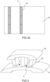
- FIG. 1 schematizes an example of a mechanical structure of the invention and highlights an active substrate 10 in which it is sought to propagate a vibration mode from an actuator 20 via an elementary amplification structure 30, comprising at least one, or even several Ti trenches, (two on the Figure 1 ) the elementary structure 30 being secured to said substrate for example by means of a layer of glue 40.
- the active substrate is oriented along a first plane defined by two orthogonal axes X and Y in an orthonormal frame (X, Y, Z).
- the trenches are oriented along a plane including a Z' axis coincident with the Z axis.
- the trenches could be oriented according to planes including a Z' axis making a non-zero angle with the Z axis.
- the positioning of several actuators on the surface of a so-called active substrate is optimized in which we seek to propagate vibrating modes and preferably a mode centered on an optimal frequency.
- the actuator 20 which may be piezoelectric, thermal or magnetic, may contract or expand.
- the actuator By bimetallic effect, due to the presence of the elementary structure 30 which connects it to the element to be deformed, the actuator generates a torque to the element to be deformed. This torque is amplified by the lever arm effect of the intermediate layer.
- the Applicants simulated the transmission of a vibration mode, which can be called “corrugated sheet”, to a substrate by means of a thin-film actuator, which is of particular interest for haptic panel applications.
- the simulations were carried out with an optimization of positioning of several actuators 20 as illustrated in Figure 2a .
- Two rows of three actuators are arranged on the surface of an intermediate silicon structure 30, in order to transfer a vibration mode to a glass slab.
- the vibration mode called “corrugated sheet” is also influenced by the dimensions of the actuators (their width and length).
- the materials cited above are indicative, essentially enabling the difference in transmission of the mode to the substrate capable of deforming under the action of the thin-layer actuator to be highlighted when an intermediate structure is present.
- the intermediate structure can thus be made up of one or more layers of various materials. It has a mechanical role allowing the actuator to be bonded and transferred to the vibrating element. It can be made up of a layer of gold, oxide, or silicon. It can also be made up, in a non-limiting manner, of a multi-layer stack of gold/silicon, oxide/silicon, or oxide/gold/silicon.
- Vibration amplitudes were simulated with arbitrary damping in air under -30V.
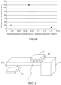
- the lever arm effect is represented diagrammatically in Figure 3 .
- the actuator By bimetallic effect, due to the presence of the intermediate amplification structure 30 which connects it to the element to be deformed 10, the actuator generates a torque, transmitted to the element to be deformed. This torque is amplified by the lever arm effect of the intermediate layer 30.
- the silicon trenches act as a lever arm by amplifying the amplitude of the mode (25 ⁇ m with the trenches in the silicon compared to 18 ⁇ m for the same thickness of silicon without trenches).
- the trenches also act as a "filter” by favoring the desired mode. Indeed, the Applicants observed that the desired mode was preserved by eliminating parasitic modes.
- the piezoelectric material can be PZT, AIN, LNO, BST or other.
- the actuator can be thermal (same principle diagram as the piezoelectric, the actuator is in this case a thermal resistance, typically a metal like aluminum or gold%) or magnetic (in this case the actuator is a magnetic material).
- the so-called active substrate can be made of glass, polymer or other.
- the amplifying structure may include intermediate layers which may be made of oxide, silicon, polysilicon, gold, etc.
- Trenches can be provided only in the silicon because this solution is easily achievable technologically. However, through trenches going from the so-called active substrate to the actuator are possible.
- the thicknesses of the materials in the amplifier structure can typically be between a hundred nanometers and a few microns, or even a few tens of microns.
- the amplification structure can be made of silicon, the glue layer being metallic, for example gold.
- This value is linked to the thickness and nature of the glass substrate that were used in simulation, namely 700 ⁇ m, but the methodology can be transcribed for other dimensions and other materials.
- Trenches that are too thin and/or too close to each other will not significantly reduce the rigidity induced by the silicon, while very wide and very distant trenches that greatly reduce the rigidity cause problems from a technical point of view. technological as a poor bond. It is therefore necessary to find the best compromise between these two effects.
- trenches of 5 to 1000 ⁇ m and spaced at a distance which can typically be between 5 and 1000 ⁇ m and more particularly with trenches having a width of 300 ⁇ m and spaced at 400 ⁇ m.
- the silicon layer can be fully sliced (trenches through the thickness of the silicon) or partially sliced as shown in the following Table 3.
- Table 3 Case Outflow trenches Partial trenches (10 ⁇ m of Si remaining) Partial trenches (20 ⁇ m of Si remaining) Substrate deformation amplitude (finite element simulation with -30V applied to the piezoelectric material 140 ⁇ m 50 ⁇ m 15 ⁇ m Main stress (main stress, relative comparison) 630 380 250
- a haptic panel works by an air blade effect, created on the surface of the panel by the latter's vibration. This vibration is generated by piezoelectric actuators glued or deposited and engraved on the plate.
- PZT is an excellent candidate for producing an actuator to obtain integrated haptic panels, presenting good performances, using low actuation voltages, in particular compared to other piezoelectric materials such as LNO or AIN.
- haptic panels are used in particular on smartphones or tablet PCs, it is necessary to use a transparent vibrating panel, which cannot therefore be made of silicon.
- the present invention is of major interest in that it makes it possible, through the use of a necessary intermediate structure, to make it an amplifier of transmitted vibration modes.
- a variant of the present invention consists of transferring the PZT actuators produced on silicon onto a glass wafer.
- PZT actuator strips made on silicon serving as an elementary substrate can be cut and fixed on a temporary substrate hereinafter called a temporary handle allowing the silicon substrate to be partially thinned or removed, then the actuator strips to be transferred and fixed on the glass slabs by metal-metal thermocompression, for example: gold-gold.
- FIG. 5 thus illustrates an example in which the deformation of an actuator 20 is amplified, via an amplification structure 30 comprising Ti trenches, said deformation being able to be transmitted and amplified to a beam for example 10, to produce a switch or a variable capacitance, equipped with a clean contact or a mobile electrode 50, opposite a fixed contact or electrode 60.
- This fixed contact or electrode is on a mechanical support on which the switch or the variable capacitance has been mounted or produced.
- this mechanical support can be a silicon substrate.
- the deformation of the beam is amplified to more quickly cause contact between the mobile element and the fixed contact, or to increase the difference in capacitance between the two electrodes facing each other.
- piezoelectric actuators 20 are produced on the surface of an elementary silicon substrate 30 intended to serve as an elementary amplification structure, comprising at least one layer of piezoelectric material between electrodes.
- the bonding of a temporary handle 80 is carried out using an adhesive 70.
- the temporary handle can be a substrate which can be made of any type of material
- the adhesive layer 70 can be made of polymer, which can be made fluid by heating.
- an operation of thinning the substrate 30 is carried out (for example by chemical-mechanical polishing).
- a metal deposit 41 for example in gold, is made on the rear face of the substrate 30, said metal deposit being intended for bonding an active substrate (such as a glass panel, for example).
- Ti trenches are produced by etching, in said substrate 30 and in the glue layer 41, from the rear face.
- the areas to be etched are previously defined by a photolithography step.
- a seventh step illustrated in figure 6g said temporary handle 80 is detached and a step of releasing the bonding layer 70 (partially as shown or totally) is also carried out at the level of said actuators 20.
- the bonding layer may be partially removed or totally removed as advantageously for polymer bonding.
- this latter operation can be carried out by raising the temperature (by any heat source) making said polymer malleable and therefore making it possible to separate the temporary substrate called the handle from the entire mechanical structure of the invention which has been produced.
Landscapes
- Engineering & Computer Science (AREA)
- Chemical & Material Sciences (AREA)
- Analytical Chemistry (AREA)
- Computer Hardware Design (AREA)
- Microelectronics & Electronic Packaging (AREA)
- Mechanical Engineering (AREA)
- Physics & Mathematics (AREA)
- Electromagnetism (AREA)
- Manufacturing & Machinery (AREA)
- Micromachines (AREA)
- Apparatuses For Generation Of Mechanical Vibrations (AREA)
Claims (17)
- Mechanische Struktur, die einen Stapel umfasst, der ein aktives Substrat (10) und mindestens einen Aktuator (20) aufweist, der zum Erzeugen von Schwingungen an dem aktiven Substrat eingerichtet ist, wobei der Stapel eine elementare Struktur zur Verstärkung der Schwingungen (30) umfasst:- die zwischen dem Aktuator (20) und dem aktiven Substrat (10) angeordnet ist, wobei die Struktur zum Übertragen und Verstärken der Schwingungen eingerichtet ist, und- die mindestens einen Graben (Ti) umfasst, der sich zwischen dem Aktuator (20) und dem aktiven Substrat (10) befindet,dadurch gekennzeichnet, dass der Graben (Ti) mindestens auf dem aktiven Substrat (10) mündet.
- Mechanische Struktur nach Anspruch 1, dadurch gekennzeichnet, dass die elementare Struktur einen Schichtstapel umfasst, von dem mindestens eine Schicht den Graben umfasst.
- Mechanische Struktur nach einem der Ansprüche 1 oder 2, dadurch gekennzeichnet, dass das Substrat eine Oberfläche aufweist, die in einer durch zwei orthogonale X- und Y-Achsen definierte ersten Ebene orientiert ist, wobei die elementare Struktur Gräben (Ti) umfasst, die periodisch entlang der ersten Ebene zwischen dem Aktuator und dem Substrat verteilt sind.
- Mechanische Struktur nach einem der Ansprüche 1 bis 3, dadurch gekennzeichnet, dass sie mehrere Aktuatoren umfasst, die mit mindestens einer elementaren Verstärkungsstruktur auf dem aktiven Substrat gekoppelt sind.
- Mechanische Struktur nach einem der Ansprüche 1 bis 4, dadurch gekennzeichnet, dass der Aktuator ein piezoelektrischer Aktuator ist.
- Mechanische Struktur nach Anspruch 5, dadurch gekennzeichnet, dass der piezoelektrische Aktuator mindestens eine Schicht aus piezoelektrischem Material umfasst, das aus PZT, AIN, LNO oder BST bestehen kann.
- Mechanische Struktur nach einem der Ansprüche 1 bis 4, dadurch gekennzeichnet, dass der Aktuator einen thermischen Widerstand umfasst, der mindestens eine Metallschicht umfassen kann, die zum Gewährleisten einer thermischen Betätigung eingerichtet ist.
- Mechanische Struktur nach einem der Ansprüche 1 bis 4, dadurch gekennzeichnet, dass der Aktuator mindestens eine Schicht aus magnetischem Material umfasst, die es ermöglicht, eine magnetische Betätigung zu gewährleisten.
- Mechanische Struktur nach einem der Ansprüche 1 bis 8, dadurch gekennzeichnet, dass das aktive Substrat ganz oder teilweise aus Glas oder Polymer oder Silizium besteht.
- Mechanische Struktur nach einem der Ansprüche 1 bis 9, dadurch gekennzeichnet, dass die elementare Struktur mindestens einen Teil aus Silizium umfasst.
- Mechanische Struktur nach den Ansprüchen 5 und 10, dadurch gekennzeichnet, dass sie Folgendes umfasst:- einen Aktuator, der eine piezoelektrische Schicht umfassen kann;- eine elementare Struktur aus Silizium;- ein aktives Glassubstrat.
- Mechanische Struktur nach Anspruch 11, dadurch gekennzeichnet, dass der Graben oder die Gräben eine Breite zwischen etwa 5 µm und 1000 µm aufweisen und im Falle von mehreren Gräben die Gräben um eine Distanz beabstandet sind, die typischerweise zwischen 5 µm und 1000 µm liegen kann.
- Verfahren zur Herstellung einer mechanischen Struktur, die einen Stapel umfasst, der ein aktives Substrat (10) und mindestens einen Aktuator (20) aufweist, der zum Erzeugen von Schwingungen an dem aktiven Substrat eingerichtet ist, wobei der Stapel eine elementare Struktur zur Verstärkung der Schwingungen (30) umfasst:- die zwischen dem Aktuator (20) und dem aktiven Substrat (10) angeordnet ist, wobei die Struktur zum Übertragen und Verstärken der Schwingungen eingerichtet ist, und- die mindestens einen Graben (Ti) umfasst, der sich zwischen dem Aktuator (20) und dem aktiven Substrat (10) befindet,wobei das Verfahren die folgenden Schritte umfasst:- Herstellen mindestens eines Aktuators (20) auf der Oberfläche eines elementaren Substrats (30);- einen Vorgang des Klebens des elementaren Substrats auf der Seite des Aktuators auf ein temporäres Substrat (80);- Herstellen mindestens eines Grabens (Ti) in dem elementaren Substrat an der Fläche, die der den Aktuator aufweisenden Fläche gegenüberliegt, wobei das elementare Substrat und der Graben eine elementare Verstärkungsstruktur bilden;- einen Vorgang des Klebens des mindestens den Graben umfassenden elementaren Substrats auf der Seite des Grabens auf das sogenannt aktive Substrat,- einen Vorgang des Entfernens des temporären Substrats, um den Aktuator freizugeben.
- Herstellungsverfahren nach Anspruch 13, dadurch gekennzeichnet, dass das elementare Substrat ganz oder teilweise aus Silizium besteht, das aktive Substrat ganz oder teilweise aus Glas besteht und der Aktuator ganz oder teilweise aus piezoelektrischem Material besteht.
- Herstellungsverfahren nach Anspruch 13 oder 14, dadurch gekennzeichnet, dass der Klebevorgang Folgendes umfasst:- Aufbringen mindestens einer Metallschicht auf die zu klebenden Flächen des elementaren Substrats bzw. des aktiven Substrats;- Kleben der die Metallschichten aufweisenden Flächen durch Thermokompression.
- Herstellungsverfahren nach einem der Ansprüche 13 bis 15, dadurch gekennzeichnet, dass es einen Vorgang des Verdünnens des elementaren Substrats von der Fläche, die der den Aktuator aufweisenden Fläche gegenüberliegt, umfasst, wobei dieser Schritt vor dem Schritt des Klebens und vor oder nach der Herstellung des Grabens durchgeführt wird.
- Herstellungsverfahren nach einem der Ansprüche 13 bis 16, dadurch gekennzeichnet, dass der Klebevorgang des temporären Substrats mit einem Polymer durchgeführt wird.
Applications Claiming Priority (2)
| Application Number | Priority Date | Filing Date | Title |
|---|---|---|---|
| FR1459430A FR3026734B1 (fr) | 2014-10-02 | 2014-10-02 | Structure mecanique comprenant un actionneur et des moyens d'amplification mecanique et procede de fabrication |
| PCT/EP2015/072536 WO2016050832A1 (fr) | 2014-10-02 | 2015-09-30 | Structure mecanique comprenant un actionneur et des moyens d'amplification mecanique et procede de fabrication |
Publications (3)
| Publication Number | Publication Date |
|---|---|
| EP3201121A1 EP3201121A1 (de) | 2017-08-09 |
| EP3201121B1 true EP3201121B1 (de) | 2025-04-23 |
| EP3201121C0 EP3201121C0 (de) | 2025-04-23 |
Family
ID=52102843
Family Applications (1)
| Application Number | Title | Priority Date | Filing Date |
|---|---|---|---|
| EP15771957.6A Active EP3201121B1 (de) | 2014-10-02 | 2015-09-30 | Mechanische struktur mit einem stellglied und mechanisches verstärkungsmittel sowie herstellungsverfahren |
Country Status (4)
| Country | Link |
|---|---|
| US (1) | US10532379B2 (de) |
| EP (1) | EP3201121B1 (de) |
| FR (1) | FR3026734B1 (de) |
| WO (1) | WO2016050832A1 (de) |
Citations (1)
| Publication number | Priority date | Publication date | Assignee | Title |
|---|---|---|---|---|
| WO2014091089A1 (fr) * | 2012-12-13 | 2014-06-19 | Dav | Interface de commande tactile |
Family Cites Families (5)
| Publication number | Priority date | Publication date | Assignee | Title |
|---|---|---|---|---|
| FR2906238B1 (fr) * | 2006-09-27 | 2008-12-19 | Commissariat Energie Atomique | Procede de realisation d'un composant electromecanique sur un substrat plan |
| US8222796B2 (en) * | 2008-10-15 | 2012-07-17 | International Business Machines Corporation | Micro-electro-mechanical device with a piezoelectric actuator |
| FR2971650B1 (fr) * | 2011-02-11 | 2013-02-22 | Commissariat Energie Atomique | Didspositif de conversion d'energie mecanique en energie electrique optimise |
| JP5725978B2 (ja) * | 2011-06-02 | 2015-05-27 | 株式会社東芝 | 超音波プローブ |
| US9815087B2 (en) * | 2013-12-12 | 2017-11-14 | Qualcomm Incorporated | Micromechanical ultrasonic transducers and display |
-
2014
- 2014-10-02 FR FR1459430A patent/FR3026734B1/fr active Active
-
2015
- 2015-09-30 EP EP15771957.6A patent/EP3201121B1/de active Active
- 2015-09-30 WO PCT/EP2015/072536 patent/WO2016050832A1/fr not_active Ceased
- 2015-09-30 US US15/515,856 patent/US10532379B2/en active Active
Patent Citations (1)
| Publication number | Priority date | Publication date | Assignee | Title |
|---|---|---|---|---|
| WO2014091089A1 (fr) * | 2012-12-13 | 2014-06-19 | Dav | Interface de commande tactile |
Also Published As
| Publication number | Publication date |
|---|---|
| US20170304867A1 (en) | 2017-10-26 |
| FR3026734A1 (fr) | 2016-04-08 |
| US10532379B2 (en) | 2020-01-14 |
| WO2016050832A1 (fr) | 2016-04-07 |
| EP3201121A1 (de) | 2017-08-09 |
| EP3201121C0 (de) | 2025-04-23 |
| FR3026734B1 (fr) | 2023-01-06 |
Similar Documents
| Publication | Publication Date | Title |
|---|---|---|
| EP3811402B1 (de) | Verfahren zur übertragung von mindestens einer materialschicht von einem ersten substrat zu einem zweiten substrat | |
| EP2663091B1 (de) | Digitaler Lautsprecher mit verbesserter Leistung | |
| EP2747452B1 (de) | Membranvorrichtung mit kontrollierter Bewegung | |
| EP2464006B1 (de) | Herstellungsverfahren eines Schallwellenresonators, der eine aufgehängte Membran umfasst | |
| EP2478393A1 (de) | Optische vorrichtung mit piezoelektrisch betätigter verformbarer membran | |
| EP1952441A1 (de) | Prozess zur herstellung einer flexiblen elektronischen einrichtung des schirmtyps, die mehrere dünnfilmkomponenten enthält | |
| FR3091414A1 (fr) | Actionneurs piézoélectriques à déformation amplifiée | |
| FR3015699A1 (fr) | Dispositif optique pour stabilisation d'images | |
| EP3065415B1 (de) | Vorrichtung mit betätigbaren membranen, und digitaler lautsprecher, der mindestens eine solche vorrichtung umfasst | |
| FR2947096A1 (fr) | Procede de realisation d'une membrane plane | |
| FR3013935B1 (fr) | Film transducteur electro-actif de son ayant une surface structuree | |
| EP3587343B1 (de) | Herstellungsverfahren einer vorrichtung, die zumindest teilweise transparent ist und eine struktur vom typ kondensator umfasst | |
| EP3201121B1 (de) | Mechanische struktur mit einem stellglied und mechanisches verstärkungsmittel sowie herstellungsverfahren | |
| EP2254243B1 (de) | Akustischer Volumenwellenresonator und Herstellungsverfahren dafür | |
| FR3073083B1 (fr) | Procede de fabrication d'un film sur un feuillet flexible | |
| EP2798668B1 (de) | Verfahren zur herstellung einer mehrschichtigen struktur auf einem substrat | |
| EP3631608B1 (de) | Verfahren zur steuerung einer mobilen vorrichtung | |
| CN111880257A (zh) | 一种可调光学滤波器件 | |
| EP3093634B1 (de) | Optischer detektor mit gekrümmter detektionsfläche | |
| JP5545190B2 (ja) | 波長可変干渉フィルターの製造方法 | |
| WO2023062139A1 (fr) | Procédé de report d'un dispositif optoélectronique | |
| EP2354832B1 (de) | Bimorphes optisches Element | |
| FR3150018A1 (fr) | Interface haptique flexible | |
| EP3350116A1 (de) | Lithographieform für nanometrischen abdruck und verfahren zur herstellung und verwendung solch einer form | |
| FR2830660A1 (fr) | Ecran plat a cristal liquide fonctionnant en mode reflectif et son procede de realisation |
Legal Events
| Date | Code | Title | Description |
|---|---|---|---|
| STAA | Information on the status of an ep patent application or granted ep patent |
Free format text: STATUS: THE INTERNATIONAL PUBLICATION HAS BEEN MADE |
|
| PUAI | Public reference made under article 153(3) epc to a published international application that has entered the european phase |
Free format text: ORIGINAL CODE: 0009012 |
|
| STAA | Information on the status of an ep patent application or granted ep patent |
Free format text: STATUS: REQUEST FOR EXAMINATION WAS MADE |
|
| 17P | Request for examination filed |
Effective date: 20170330 |
|
| AK | Designated contracting states |
Kind code of ref document: A1 Designated state(s): AL AT BE BG CH CY CZ DE DK EE ES FI FR GB GR HR HU IE IS IT LI LT LU LV MC MK MT NL NO PL PT RO RS SE SI SK SM TR |
|
| AX | Request for extension of the european patent |
Extension state: BA ME |
|
| DAV | Request for validation of the european patent (deleted) | ||
| DAX | Request for extension of the european patent (deleted) | ||
| TPAC | Observations filed by third parties |
Free format text: ORIGINAL CODE: EPIDOSNTIPA |
|
| STAA | Information on the status of an ep patent application or granted ep patent |
Free format text: STATUS: EXAMINATION IS IN PROGRESS |
|
| 17Q | First examination report despatched |
Effective date: 20201209 |
|
| RAP3 | Party data changed (applicant data changed or rights of an application transferred) |
Owner name: UNIVERSITE GRENOBLE ALPES Owner name: COMMISSARIAT A L'ENERGIE ATOMIQUE ET AUX ENERGIESALTERNATIVES |
|
| GRAP | Despatch of communication of intention to grant a patent |
Free format text: ORIGINAL CODE: EPIDOSNIGR1 |
|
| STAA | Information on the status of an ep patent application or granted ep patent |
Free format text: STATUS: GRANT OF PATENT IS INTENDED |
|
| RIC1 | Information provided on ipc code assigned before grant |
Ipc: H10N 30/20 20230101ALI20241216BHEP Ipc: B81B 3/00 20060101AFI20241216BHEP |
|
| INTG | Intention to grant announced |
Effective date: 20250113 |
|
| GRAS | Grant fee paid |
Free format text: ORIGINAL CODE: EPIDOSNIGR3 |
|
| GRAA | (expected) grant |
Free format text: ORIGINAL CODE: 0009210 |
|
| STAA | Information on the status of an ep patent application or granted ep patent |
Free format text: STATUS: THE PATENT HAS BEEN GRANTED |
|
| AK | Designated contracting states |
Kind code of ref document: B1 Designated state(s): AL AT BE BG CH CY CZ DE DK EE ES FI FR GB GR HR HU IE IS IT LI LT LU LV MC MK MT NL NO PL PT RO RS SE SI SK SM TR |
|
| REG | Reference to a national code |
Ref country code: GB Ref legal event code: FG4D Free format text: NOT ENGLISH |
|
| REG | Reference to a national code |
Ref country code: CH Ref legal event code: EP |
|
| REG | Reference to a national code |
Ref country code: IE Ref legal event code: FG4D Free format text: LANGUAGE OF EP DOCUMENT: FRENCH |
|
| RAP4 | Party data changed (patent owner data changed or rights of a patent transferred) |
Owner name: UNIVERSITE GRENOBLE ALPES Owner name: COMMISSARIAT A L'ENERGIE ATOMIQUE ET AUX ENERGIESALTERNATIVES |
|
| U01 | Request for unitary effect filed |
Effective date: 20250425 |
|
| U07 | Unitary effect registered |
Designated state(s): AT BE BG DE DK EE FI FR IT LT LU LV MT NL PT RO SE SI Effective date: 20250430 |
|
| PG25 | Lapsed in a contracting state [announced via postgrant information from national office to epo] |
Ref country code: ES Free format text: LAPSE BECAUSE OF FAILURE TO SUBMIT A TRANSLATION OF THE DESCRIPTION OR TO PAY THE FEE WITHIN THE PRESCRIBED TIME-LIMIT Effective date: 20250423 |
|
| PG25 | Lapsed in a contracting state [announced via postgrant information from national office to epo] |
Ref country code: NO Free format text: LAPSE BECAUSE OF FAILURE TO SUBMIT A TRANSLATION OF THE DESCRIPTION OR TO PAY THE FEE WITHIN THE PRESCRIBED TIME-LIMIT Effective date: 20250723 Ref country code: GR Free format text: LAPSE BECAUSE OF FAILURE TO SUBMIT A TRANSLATION OF THE DESCRIPTION OR TO PAY THE FEE WITHIN THE PRESCRIBED TIME-LIMIT Effective date: 20250724 |
|
| PG25 | Lapsed in a contracting state [announced via postgrant information from national office to epo] |
Ref country code: PL Free format text: LAPSE BECAUSE OF FAILURE TO SUBMIT A TRANSLATION OF THE DESCRIPTION OR TO PAY THE FEE WITHIN THE PRESCRIBED TIME-LIMIT Effective date: 20250423 |
|
| PGFP | Annual fee paid to national office [announced via postgrant information from national office to epo] |
Ref country code: GB Payment date: 20250923 Year of fee payment: 11 |
|
| PG25 | Lapsed in a contracting state [announced via postgrant information from national office to epo] |
Ref country code: HR Free format text: LAPSE BECAUSE OF FAILURE TO SUBMIT A TRANSLATION OF THE DESCRIPTION OR TO PAY THE FEE WITHIN THE PRESCRIBED TIME-LIMIT Effective date: 20250423 |
|
| PG25 | Lapsed in a contracting state [announced via postgrant information from national office to epo] |
Ref country code: RS Free format text: LAPSE BECAUSE OF FAILURE TO SUBMIT A TRANSLATION OF THE DESCRIPTION OR TO PAY THE FEE WITHIN THE PRESCRIBED TIME-LIMIT Effective date: 20250723 |
|
| PG25 | Lapsed in a contracting state [announced via postgrant information from national office to epo] |
Ref country code: IS Free format text: LAPSE BECAUSE OF FAILURE TO SUBMIT A TRANSLATION OF THE DESCRIPTION OR TO PAY THE FEE WITHIN THE PRESCRIBED TIME-LIMIT Effective date: 20250823 |
|
| U20 | Renewal fee for the european patent with unitary effect paid |
Year of fee payment: 11 Effective date: 20250923 |
|
| PG25 | Lapsed in a contracting state [announced via postgrant information from national office to epo] |
Ref country code: SM Free format text: LAPSE BECAUSE OF FAILURE TO SUBMIT A TRANSLATION OF THE DESCRIPTION OR TO PAY THE FEE WITHIN THE PRESCRIBED TIME-LIMIT Effective date: 20250423 |
|
| PG25 | Lapsed in a contracting state [announced via postgrant information from national office to epo] |
Ref country code: CZ Free format text: LAPSE BECAUSE OF FAILURE TO SUBMIT A TRANSLATION OF THE DESCRIPTION OR TO PAY THE FEE WITHIN THE PRESCRIBED TIME-LIMIT Effective date: 20250423 |
|
| PG25 | Lapsed in a contracting state [announced via postgrant information from national office to epo] |
Ref country code: SK Free format text: LAPSE BECAUSE OF FAILURE TO SUBMIT A TRANSLATION OF THE DESCRIPTION OR TO PAY THE FEE WITHIN THE PRESCRIBED TIME-LIMIT Effective date: 20250423 |