EP3200334A1 - Dc-dc converter and associated control method - Google Patents
Dc-dc converter and associated control method Download PDFInfo
- Publication number
- EP3200334A1 EP3200334A1 EP16178971.4A EP16178971A EP3200334A1 EP 3200334 A1 EP3200334 A1 EP 3200334A1 EP 16178971 A EP16178971 A EP 16178971A EP 3200334 A1 EP3200334 A1 EP 3200334A1
- Authority
- EP
- European Patent Office
- Prior art keywords
- current
- converter
- inductor
- node
- pull
- Prior art date
- Legal status (The legal status is an assumption and is not a legal conclusion. Google has not performed a legal analysis and makes no representation as to the accuracy of the status listed.)
- Granted
Links
Images

Classifications
-
- H—ELECTRICITY
- H02—GENERATION; CONVERSION OR DISTRIBUTION OF ELECTRIC POWER
- H02M—APPARATUS FOR CONVERSION BETWEEN AC AND AC, BETWEEN AC AND DC, OR BETWEEN DC AND DC, AND FOR USE WITH MAINS OR SIMILAR POWER SUPPLY SYSTEMS; CONVERSION OF DC OR AC INPUT POWER INTO SURGE OUTPUT POWER; CONTROL OR REGULATION THEREOF
- H02M3/00—Conversion of DC power input into DC power output
- H02M3/02—Conversion of DC power input into DC power output without intermediate conversion into AC
- H02M3/04—Conversion of DC power input into DC power output without intermediate conversion into AC by static converters
- H02M3/10—Conversion of DC power input into DC power output without intermediate conversion into AC by static converters using discharge tubes with control electrode or semiconductor devices with control electrode
- H02M3/145—Conversion of DC power input into DC power output without intermediate conversion into AC by static converters using discharge tubes with control electrode or semiconductor devices with control electrode using devices of a triode or transistor type requiring continuous application of a control signal
- H02M3/155—Conversion of DC power input into DC power output without intermediate conversion into AC by static converters using discharge tubes with control electrode or semiconductor devices with control electrode using devices of a triode or transistor type requiring continuous application of a control signal using semiconductor devices only
- H02M3/156—Conversion of DC power input into DC power output without intermediate conversion into AC by static converters using discharge tubes with control electrode or semiconductor devices with control electrode using devices of a triode or transistor type requiring continuous application of a control signal using semiconductor devices only with automatic control of output voltage or current, e.g. switching regulators
- H02M3/158—Conversion of DC power input into DC power output without intermediate conversion into AC by static converters using discharge tubes with control electrode or semiconductor devices with control electrode using devices of a triode or transistor type requiring continuous application of a control signal using semiconductor devices only with automatic control of output voltage or current, e.g. switching regulators including plural semiconductor devices as final control devices for a single load
-
- H—ELECTRICITY
- H02—GENERATION; CONVERSION OR DISTRIBUTION OF ELECTRIC POWER
- H02M—APPARATUS FOR CONVERSION BETWEEN AC AND AC, BETWEEN AC AND DC, OR BETWEEN DC AND DC, AND FOR USE WITH MAINS OR SIMILAR POWER SUPPLY SYSTEMS; CONVERSION OF DC OR AC INPUT POWER INTO SURGE OUTPUT POWER; CONTROL OR REGULATION THEREOF
- H02M3/00—Conversion of DC power input into DC power output
- H02M3/02—Conversion of DC power input into DC power output without intermediate conversion into AC
- H02M3/04—Conversion of DC power input into DC power output without intermediate conversion into AC by static converters
- H02M3/10—Conversion of DC power input into DC power output without intermediate conversion into AC by static converters using discharge tubes with control electrode or semiconductor devices with control electrode
- H02M3/145—Conversion of DC power input into DC power output without intermediate conversion into AC by static converters using discharge tubes with control electrode or semiconductor devices with control electrode using devices of a triode or transistor type requiring continuous application of a control signal
- H02M3/155—Conversion of DC power input into DC power output without intermediate conversion into AC by static converters using discharge tubes with control electrode or semiconductor devices with control electrode using devices of a triode or transistor type requiring continuous application of a control signal using semiconductor devices only
- H02M3/156—Conversion of DC power input into DC power output without intermediate conversion into AC by static converters using discharge tubes with control electrode or semiconductor devices with control electrode using devices of a triode or transistor type requiring continuous application of a control signal using semiconductor devices only with automatic control of output voltage or current, e.g. switching regulators
- H02M3/1563—Conversion of DC power input into DC power output without intermediate conversion into AC by static converters using discharge tubes with control electrode or semiconductor devices with control electrode using devices of a triode or transistor type requiring continuous application of a control signal using semiconductor devices only with automatic control of output voltage or current, e.g. switching regulators without using an external clock
-
- H—ELECTRICITY
- H02—GENERATION; CONVERSION OR DISTRIBUTION OF ELECTRIC POWER
- H02M—APPARATUS FOR CONVERSION BETWEEN AC AND AC, BETWEEN AC AND DC, OR BETWEEN DC AND DC, AND FOR USE WITH MAINS OR SIMILAR POWER SUPPLY SYSTEMS; CONVERSION OF DC OR AC INPUT POWER INTO SURGE OUTPUT POWER; CONTROL OR REGULATION THEREOF
- H02M1/00—Details of apparatus for conversion
- H02M1/08—Circuits specially adapted for the generation of control voltages for semiconductor devices incorporated in static converters
-
- H—ELECTRICITY
- H02—GENERATION; CONVERSION OR DISTRIBUTION OF ELECTRIC POWER
- H02M—APPARATUS FOR CONVERSION BETWEEN AC AND AC, BETWEEN AC AND DC, OR BETWEEN DC AND DC, AND FOR USE WITH MAINS OR SIMILAR POWER SUPPLY SYSTEMS; CONVERSION OF DC OR AC INPUT POWER INTO SURGE OUTPUT POWER; CONTROL OR REGULATION THEREOF
- H02M1/00—Details of apparatus for conversion
- H02M1/08—Circuits specially adapted for the generation of control voltages for semiconductor devices incorporated in static converters
- H02M1/088—Circuits specially adapted for the generation of control voltages for semiconductor devices incorporated in static converters for the simultaneous control of series or parallel connected semiconductor devices
-
- G—PHYSICS
- G05—CONTROLLING; REGULATING
- G05F—SYSTEMS FOR REGULATING ELECTRIC OR MAGNETIC VARIABLES
- G05F1/00—Automatic systems in which deviations of an electric quantity from one or more predetermined values are detected at the output of the system and fed back to a device within the system to restore the detected quantity to its predetermined value or values, i.e. retroactive systems
- G05F1/10—Regulating voltage or current
- G05F1/46—Regulating voltage or current wherein the variable actually regulated by the final control device is DC
- G05F1/618—Regulating voltage or current wherein the variable actually regulated by the final control device is DC using semiconductor devices in series and in parallel with the load as final control devices
-
- H—ELECTRICITY
- H02—GENERATION; CONVERSION OR DISTRIBUTION OF ELECTRIC POWER
- H02M—APPARATUS FOR CONVERSION BETWEEN AC AND AC, BETWEEN AC AND DC, OR BETWEEN DC AND DC, AND FOR USE WITH MAINS OR SIMILAR POWER SUPPLY SYSTEMS; CONVERSION OF DC OR AC INPUT POWER INTO SURGE OUTPUT POWER; CONTROL OR REGULATION THEREOF
- H02M1/00—Details of apparatus for conversion
- H02M1/0003—Details of control, feedback or regulation circuits
-
- H—ELECTRICITY
- H02—GENERATION; CONVERSION OR DISTRIBUTION OF ELECTRIC POWER
- H02M—APPARATUS FOR CONVERSION BETWEEN AC AND AC, BETWEEN AC AND DC, OR BETWEEN DC AND DC, AND FOR USE WITH MAINS OR SIMILAR POWER SUPPLY SYSTEMS; CONVERSION OF DC OR AC INPUT POWER INTO SURGE OUTPUT POWER; CONTROL OR REGULATION THEREOF
- H02M1/00—Details of apparatus for conversion
- H02M1/0003—Details of control, feedback or regulation circuits
- H02M1/0009—Devices or circuits for detecting current in a converter
-
- H—ELECTRICITY
- H02—GENERATION; CONVERSION OR DISTRIBUTION OF ELECTRIC POWER
- H02M—APPARATUS FOR CONVERSION BETWEEN AC AND AC, BETWEEN AC AND DC, OR BETWEEN DC AND DC, AND FOR USE WITH MAINS OR SIMILAR POWER SUPPLY SYSTEMS; CONVERSION OF DC OR AC INPUT POWER INTO SURGE OUTPUT POWER; CONTROL OR REGULATION THEREOF
- H02M1/00—Details of apparatus for conversion
- H02M1/0045—Converters combining the concepts of switch-mode regulation and linear regulation, e.g. linear pre-regulator to switching converter, linear and switching converter in parallel, same converter or same transistor operating either in linear or switching mode
-
- H—ELECTRICITY
- H02—GENERATION; CONVERSION OR DISTRIBUTION OF ELECTRIC POWER
- H02M—APPARATUS FOR CONVERSION BETWEEN AC AND AC, BETWEEN AC AND DC, OR BETWEEN DC AND DC, AND FOR USE WITH MAINS OR SIMILAR POWER SUPPLY SYSTEMS; CONVERSION OF DC OR AC INPUT POWER INTO SURGE OUTPUT POWER; CONTROL OR REGULATION THEREOF
- H02M3/00—Conversion of DC power input into DC power output
- H02M3/02—Conversion of DC power input into DC power output without intermediate conversion into AC
- H02M3/04—Conversion of DC power input into DC power output without intermediate conversion into AC by static converters
- H02M3/10—Conversion of DC power input into DC power output without intermediate conversion into AC by static converters using discharge tubes with control electrode or semiconductor devices with control electrode
- H02M3/145—Conversion of DC power input into DC power output without intermediate conversion into AC by static converters using discharge tubes with control electrode or semiconductor devices with control electrode using devices of a triode or transistor type requiring continuous application of a control signal
- H02M3/155—Conversion of DC power input into DC power output without intermediate conversion into AC by static converters using discharge tubes with control electrode or semiconductor devices with control electrode using devices of a triode or transistor type requiring continuous application of a control signal using semiconductor devices only
- H02M3/156—Conversion of DC power input into DC power output without intermediate conversion into AC by static converters using discharge tubes with control electrode or semiconductor devices with control electrode using devices of a triode or transistor type requiring continuous application of a control signal using semiconductor devices only with automatic control of output voltage or current, e.g. switching regulators
- H02M3/1566—Conversion of DC power input into DC power output without intermediate conversion into AC by static converters using discharge tubes with control electrode or semiconductor devices with control electrode using devices of a triode or transistor type requiring continuous application of a control signal using semiconductor devices only with automatic control of output voltage or current, e.g. switching regulators with means for compensating against rapid load changes, e.g. with auxiliary current source, with dual mode control or with inductance variation
Definitions
- a settling time (transition time) is preferred to be as short as possible.
- the settling time is related to an inductance of an inductor within the DC-DC converter, and the smaller inductance results in a shorter setting time.
- the smaller inductance may cause a large ripple on the output voltage. Therefore, the tradeoff between the settling time and the ripple becomes a problem to a designer.
- a DC-DC converter for converting an input voltage to an output voltage at an output node.
- the DC-DC converter comprises an inductor, a switch module, a pull-up circuit and a pull-down circuit.
- the inductor has a first node and a second node, wherein the second node is coupled to the output node of the DC-DC converter.
- the switch module is arranged for selectively connecting the input voltage or a ground voltage to the first node of the inductor according to a driving signal.
- the pull-up circuit is coupled to the output node of the DC-DC converter, and is arranged for selectively providing a first current to the output node of the DC-DC converter.
- the pull-down circuit is coupled to the output node of the DC-DC converter, and is arranged for selectively sinking a second current from the output node of the DC-DC converter.
- at least one of the first current provided by the pull-up circuit and the second current sunk by the pull-down circuit is determined based on an inductor current flowing through the inductor.
- a method for controlling a DC-DC converter comprises an inductor and a switch module, the inductor has a first node and a second node, the second node is coupled to an output node of the DC-DC converter, and the switch module selectively connects the input voltage or a ground voltage to the first node of the inductor according to a driving signal; and the method comprises: selectively providing a first current to the output node of the DC-DC converter; and selectively sinking a second current from the output node of the DC-DC converter; wherein at least one of the first current and the second current are determined based on an inductor current flowing through the inductor.
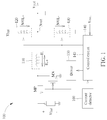
- FIG. 1 is a diagram illustrating a DC-DC converter 100 according to one embodiment of the present invention.
- the DC-DC converter 100 comprises a switch module comprising two switches MP and MN, an inductor 110, a pull-up circuit 1 20, a pull-down circuit 130, a control circuit 140, a driver 1 50 and a current detector 160.
- the DC-DC converter 100 is used to receive an input voltage, such as a battery voltage Vbat, to generate an output voltage Vout at an output node.
- the switch MP is arranged to selectively connect the input voltage Vbat to a first node of the inductor 110 according a driving signal outputted by the driver 1 50
- the switch MN is arranged to selectively connect a ground voltage to the first node of the inductor 110 according the driving signal outputted by the driver 150.
- the driving signal outputted by the driver 1 50 is a pulse width modulation (PWM) signal, and a duty cycle of the driving signal is determined based on a current level of output voltage Vout and a desired level of the output voltage Vout.
- PWM pulse width modulation
- the control circuit 140 may control the driver 1 50 to adjust the duty cycle of the driving signal (in this embodiment, the duty cycle decreases), to increase the output voltage Vout.
- the duty cycle decreases
- the control circuit 140 may control the driver 1 50 to adjust the duty cycle of the driving signal (in this embodiment, the duty cycle decreases), to increase the output voltage Vout.
- the driving signal is at a low level
- the switch MN is off and the switch MP is on
- an inductor current IL+ charging current
- the switch MP is off and the switch MN is on
- an inductor current IL- discretharging current
- the pull-up circuit 120 is arranged to provide a current to the output node Nout when the battery charges the output node Nout, and the pull-down circuit 130 is arranged to sink a current from the output node Nout when the output node Nout is discharged.
- the currents provided by the pull-up circuit 120 and the pull-down circuit 130 are a function of the inductor current of the inductor 110.
- the currents provided by the pull-up circuit 120 and the pull-down circuit 130 have a positive relationship with the inductor current, for example, the current provided by the pull-up circuit 120 may equal to N*IL+, and the current provided by the pull-down circuit 130 may equal to N*IL-, where N can be any suitable values.
- the switch MP when the output voltage is set to be higher, the switch MP is turned on to make the inductor current IL+ (charging current) to flow from the battery to the output node Nout, the current detector 160 detects the inductor current IL+ to generate a detecting result, and the control circuit 140 controls the pull-up circuit 120 to provide the current (N*IL+) to the output node Nout, and at this time the pull-down circuit 130 is disabled.
- IL+ charging current
- the switch MN is turned on to make the inductor current IL-(discharging current) to flow from the output node Nout to the ground
- the current detector 160 detects the inductor current IL- to generate a detecting result
- the control circuit 140 controls the pull-down circuit 130 to sink the current (N*IL-) from the output node Nout, and at this time the pull-up circuit 120 is disabled.
- FIG. 2 shows timing diagrams of the output voltage Vout and an output current iout of the DC-DC converter when DC-DC converter 100 raises the output voltage Vout.
- the solid line is for the DC-DC converter 100
- the dotted line is for the DC-DC converter without the pull-up circuit 1 20 and the pull-down circuit 130.
- the charging current is equal to (Vbat-Vout)/(L*(N+1)), and the output voltage Vout can raise to the desired level faster (i.e. the settling time is shorten).
- the current provided by the pull-up circuit 120 is a multiple of the inductor current IL+ (i.e.
- the DC-DC converter 100 can have the shorter settling time without using the inductor having smaller inductance actually, thereby the ripple issue can be alleviated.
- the charging current i.e. the output current iout
- the response of the circuits can be controlled easily, and the loop control can be simplified.
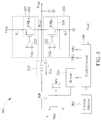
- FIG. 3 is a diagram illustrating a DC-DC converter 300 according to another embodiment of the present invention.
- the DC-DC converter 300 comprises a switch module comprising two switches MP and MN, an inductor 310, a pull-up circuit 320, a pull-down circuit 330, a control circuit 340, a driver 350 and a current detector 360.
- the DC-DC converter 300 is used to receive an input voltage, such as a battery voltage Vbat, to generate an output voltage Vout at an output node.
- the pull-up circuit 320 comprises an operational amplifier 322, a transistor 324 and a resistor R1, where a negative input node of the operational amplifier 322 is coupled to a source electrode of the transistor 324, and a positive input node of the operational amplifier 322 receives a first reference voltage VR1 outputted by the control circuit 340.
- the pull-down circuit 330 comprises an operational amplifier 332, a transistor 334 and a resistor R2, where a negative input node of the operational amplifier 332 is coupled to a source electrode of the transistor 334, and a positive input node of the operational amplifier 332 receives a second reference voltage VR2 outputted by the control circuit 340.
- the switch MP is arranged to selectively connect the input voltage Vbat to a first node of the inductor 310 according a driving signal outputted by the driver 350
- the switch MN is arranged to selectively connect a ground voltage to the first node of the inductor 310 according the driving signal outputted by the driver 350.
- the driving signal outputted by the driver 350 is a pulse width modulation (PWM) signal, and a duty cycle of the driving signal is determined based on a current level of output voltage Vout and a desired level of the output voltage Vout.
- PWM pulse width modulation
- the control circuit 340 may control the driver 350 to adjust the duty cycle of the driving signal (in this embodiment, the duty cycle decreases), to increase the output voltage Vout.
- the duty cycle decreases
- the driving signal is at a low level
- the switch MN is off and the switch MP is on
- an inductor current IL+ charging current
- the switch MP is off and the switch MN is on
- an inductor current IL- discretharging current
- the pull-up circuit 320 is arranged to provide a current to the output node Nout when the battery charges the output node Nout
- the pull-down circuit 330 is arranged to sink a current from the output node Nout when the output node Nout is discharged.
- the currents provided by the pull-up circuit 320 and the pull-down circuit 330 are a function of the inductor current of the inductor 310.
- the currents provided by the pull-up circuit 320 and the pull-down circuit 330 have a positive relationship with the inductor current, for example, the current provided by the pull-up circuit 320 may equal to N*IL+, and the current provided by the pull-down circuit 330 may equal to N*IL-, where N can be any suitable values.
- the current detector 360 detects the inductor current IL+ to generate a detecting result.
- the current detector 360 may use a current mirror to sense the current flowing through the switch MP to generate the detecting result.
- the control circuit 340 generates the first reference voltage VR1 to the positive input node of the operational amplifier 322 according to the detecting result.
- the control circuit 340 generates the lower first reference signal VR1 to the positive input node of the operational amplifier 322, to make the current provided by the pull-up circuit 320 always substantially equal to (N*IL+).
- the current detector 360 detects the inductor current IL- to generate a detecting result.
- the current detector 360 may use a current mirror to sense the current flowing through the switch MN to generate the detecting result.
- the control circuit 340 generates the second reference voltage VR2 to the positive input node of the operational amplifier 332 according to the detecting result.
- the control circuit 340 generates the lower second reference signal VR2 to the positive input node of the operational amplifier 332, to make the current provided by the pull-down circuit 330 always substantially equal to (N*IL-).
- the DC-DC converter of the present invention additional charging paths are arranged to shorten the setting time, and the currents provided by the additional charging current are a function of the inductor current. Therefore, the DC-DC converter can have the shorter settling time without using the inductor having smaller inductance actually to alleviate the ripple issue, and the response of the circuits can be controlled easily, and the loop control can be simplified.
Landscapes
- Engineering & Computer Science (AREA)
- Power Engineering (AREA)
- Dc-Dc Converters (AREA)
Description
- When a DC-DC converter is used to convert an input voltage to a desired output voltage, a settling time (transition time) is preferred to be as short as possible. The settling time is related to an inductance of an inductor within the DC-DC converter, and the smaller inductance results in a shorter setting time. However, the smaller inductance may cause a large ripple on the output voltage. Therefore, the tradeoff between the settling time and the ripple becomes a problem to a designer.
- Conventional art provides a converter having additional charging path to shorten the settling time, however, the response of the circuits is generally difficult to control due to the inappropriate setting of the current provided by this additional charging path.
- It is therefore an objective of the present invention to provide a DC-DC converter, which includes an additional charging path to shorten the setting time, and the current provided by the additional charging path is determined based on an inductor current flowing through the inductor within the DC-DC converter, to solve the above-mentioned problem.
- This is achieved by a DC-DC converter according to
claim 1, and a method according to claim 14. The dependent claims pertain to corresponding further developments and improvements. - As will be seen more clearly from the detailed description following below, a DC-DC converter for converting an input voltage to an output voltage at an output node is provided. The DC-DC converter comprises an inductor, a switch module, a pull-up circuit and a pull-down circuit. The inductor has a first node and a second node, wherein the second node is coupled to the output node of the DC-DC converter. The switch module is arranged for selectively connecting the input voltage or a ground voltage to the first node of the inductor according to a driving signal. The pull-up circuit is coupled to the output node of the DC-DC converter, and is arranged for selectively providing a first current to the output node of the DC-DC converter. The pull-down circuit is coupled to the output node of the DC-DC converter, and is arranged for selectively sinking a second current from the output node of the DC-DC converter. In addition, at least one of the first current provided by the pull-up circuit and the second current sunk by the pull-down circuit is determined based on an inductor current flowing through the inductor.
- As will be seen more clearly from the detailed description following below, a method for controlling a DC-DC converter is provided, wherein the DC-DC converter comprises an inductor and a switch module, the inductor has a first node and a second node, the second node is coupled to an output node of the DC-DC converter, and the switch module selectively connects the input voltage or a ground voltage to the first node of the inductor according to a driving signal; and the method comprises: selectively providing a first current to the output node of the DC-DC converter; and selectively sinking a second current from the output node of the DC-DC converter; wherein at least one of the first current and the second current are determined based on an inductor current flowing through the inductor.
- These and other objectives of the present invention will no doubt become obvious to those of ordinary skill in the art after reading the following detailed description of the preferred embodiment that is illustrated in the various figures and drawings.
-
-
FIG. 1 is a diagram illustrating a DC-DC converter according to one embodiment of the present invention. -
FIG. 2 shows timing diagrams of the output voltage and an output current of the DC-DC converter when DC-DC converter raises the output voltage. -
FIG. 3 is a diagram illustrating a DC-DC converter according to another embodiment of the present invention. - Certain terms are used throughout the following description and claims to refer to particular system components. As one skilled in the art will appreciate, manufacturers may refer to a component by different names. This document does not intend to distinguish between components that differ in name but not function. In the following discussion and in the claims, the terms "including" and "comprising" are used in an open-ended fashion, and thus should be interpreted to mean "including, but not limited to ..." The terms "couple" and "couples" are intended to mean either an indirect or a direct electrical connection. Thus, if a first device couples to a second device, that connection may be through a direct electrical connection, or through an indirect electrical connection via other devices and connections.
- Please refer to
FIG. 1 , which is a diagram illustrating a DC-DC converter 100 according to one embodiment of the present invention. As shown inFIG. 1 , the DC-DC converter 100 comprises a switch module comprising two switches MP and MN, aninductor 110, a pull-up circuit 1 20, a pull-down circuit 130, acontrol circuit 140, adriver 1 50 and acurrent detector 160. In this embodiment, the DC-DC converter 100 is used to receive an input voltage, such as a battery voltage Vbat, to generate an output voltage Vout at an output node. - In the operations of the DC-
DC converter 100, the switch MP is arranged to selectively connect the input voltage Vbat to a first node of theinductor 110 according a driving signal outputted by thedriver 1 50, and the switch MN is arranged to selectively connect a ground voltage to the first node of theinductor 110 according the driving signal outputted by thedriver 150. In this embodiment, the driving signal outputted by thedriver 1 50 is a pulse width modulation (PWM) signal, and a duty cycle of the driving signal is determined based on a current level of output voltage Vout and a desired level of the output voltage Vout. In detail, when the DC-DC converter 100 needs to raise the output voltage Vout, thecontrol circuit 140 may control thedriver 1 50 to adjust the duty cycle of the driving signal (in this embodiment, the duty cycle decreases), to increase the output voltage Vout. For example, when the driving signal is at a low level, the switch MN is off and the switch MP is on, and an inductor current IL+ (charging current) flows from the battery to the output node Nout to increase the output voltage Vout; and when the driving signal is at a high level, the switch MP is off and the switch MN is on, and an inductor current IL- (discharging current) flows from the output node Nout to the ground to decrease the output voltage Vout. By alternately enabling the switches MP and MN, the output node Nout is alternately charged and discharged to reach the desired output voltage. - In addition, to improve the settling time of the DC-
DC converter 100 when the DC-DC converter 100 needs to raise the output voltage Vout, the pull-up circuit 120 is arranged to provide a current to the output node Nout when the battery charges the output node Nout, and the pull-down circuit 130 is arranged to sink a current from the output node Nout when the output node Nout is discharged. Particularly, the currents provided by the pull-up circuit 120 and the pull-down circuit 130 are a function of the inductor current of theinductor 110. In one embodiment, the currents provided by the pull-up circuit 120 and the pull-down circuit 130 have a positive relationship with the inductor current, for example, the current provided by the pull-upcircuit 120 may equal to N*IL+, and the current provided by the pull-down circuit 130 may equal to N*IL-, where N can be any suitable values. - In detail, when the output voltage is set to be higher, the switch MP is turned on to make the inductor current IL+ (charging current) to flow from the battery to the output node Nout, the
current detector 160 detects the inductor current IL+ to generate a detecting result, and thecontrol circuit 140 controls the pull-up circuit 120 to provide the current (N*IL+) to the output node Nout, and at this time the pull-down circuit 130 is disabled. In addition, when the output voltage is set to be lower, the switch MN is turned on to make the inductor current IL-(discharging current) to flow from the output node Nout to the ground, thecurrent detector 160 detects the inductor current IL- to generate a detecting result, and thecontrol circuit 140 controls the pull-down circuit 130 to sink the current (N*IL-) from the output node Nout, and at this time the pull-up circuit 120 is disabled. -
FIG. 2 shows timing diagrams of the output voltage Vout and an output current iout of the DC-DC converter when DC-DC converter 100 raises the output voltage Vout. The solid line is for the DC-DC converter 100, and the dotted line is for the DC-DC converter without the pull-up circuit 1 20 and the pull-down circuit 130. As shown inFIG. 2 , because of the use of the pull-up circuit 120 and the pull-down circuit 130, the charging current is equal to (Vbat-Vout)/(L*(N+1)), and the output voltage Vout can raise to the desired level faster (i.e. the settling time is shorten). In addition, because the current provided by the pull-up circuit 120 is a multiple of the inductor current IL+ (i.e. N*IL+), it is equivalent that the charging current is generated by a smaller inductor whose inductance is (L/(N+1)), where "L" is the inductance of theinductor 110. Therefore, the DC-DC converter 100 can have the shorter settling time without using the inductor having smaller inductance actually, thereby the ripple issue can be alleviated. - Furthermore, because the current provided by the pull-
up circuit 120 is a function of the inductor current IL+, the charging current (i.e. the output current iout) can be regarded as the function of the inductor current IL+. Therefore, the response of the circuits can be controlled easily, and the loop control can be simplified. - Please refer to
FIG. 3 , which is a diagram illustrating a DC-DC converter 300 according to another embodiment of the present invention. As shown inFIG. 3 , the DC-DC converter 300 comprises a switch module comprising two switches MP and MN, aninductor 310, a pull-up circuit 320, a pull-down circuit 330, acontrol circuit 340, adriver 350 and acurrent detector 360. In this embodiment, the DC-DC converter 300 is used to receive an input voltage, such as a battery voltage Vbat, to generate an output voltage Vout at an output node. - In this embodiment, the pull-
up circuit 320 comprises anoperational amplifier 322, atransistor 324 and a resistor R1, where a negative input node of theoperational amplifier 322 is coupled to a source electrode of thetransistor 324, and a positive input node of theoperational amplifier 322 receives a first reference voltage VR1 outputted by thecontrol circuit 340. The pull-down circuit 330 comprises anoperational amplifier 332, atransistor 334 and a resistor R2, where a negative input node of theoperational amplifier 332 is coupled to a source electrode of thetransistor 334, and a positive input node of theoperational amplifier 332 receives a second reference voltage VR2 outputted by thecontrol circuit 340. - In the operations of the DC-
DC converter 300, the switch MP is arranged to selectively connect the input voltage Vbat to a first node of theinductor 310 according a driving signal outputted by thedriver 350, and the switch MN is arranged to selectively connect a ground voltage to the first node of theinductor 310 according the driving signal outputted by thedriver 350. In this embodiment, the driving signal outputted by thedriver 350 is a pulse width modulation (PWM) signal, and a duty cycle of the driving signal is determined based on a current level of output voltage Vout and a desired level of the output voltage Vout. In detail, when the DC-DC converter 300 needs to raise the output voltage Vout, thecontrol circuit 340 may control thedriver 350 to adjust the duty cycle of the driving signal (in this embodiment, the duty cycle decreases), to increase the output voltage Vout. For example, when the driving signal is at a low level, the switch MN is off and the switch MP is on, and an inductor current IL+ (charging current) flows from the battery to the output node Nout to increase the output voltage Vout; and when the driving signal is at a high level, the switch MP is off and the switch MN is on, and an inductor current IL- (discharging current) flows from the output node Nout to the ground to decrease the output voltage Vout. By alternately enabling the switches MP and MN, the output node Nout will reach the desired output voltage. - In addition, to improve the settling time of the DC-
DC converter 300 when the DC-DC converter 300 needs to raise the output voltage Vout, the pull-up circuit 320 is arranged to provide a current to the output node Nout when the battery charges the output node Nout, and the pull-down circuit 330 is arranged to sink a current from the output node Nout when the output node Nout is discharged. Particularly, the currents provided by the pull-up circuit 320 and the pull-down circuit 330 are a function of the inductor current of theinductor 310. In one embodiment, the currents provided by the pull-up circuit 320 and the pull-down circuit 330 have a positive relationship with the inductor current, for example, the current provided by the pull-up circuit 320 may equal to N*IL+, and the current provided by the pull-down circuit 330 may equal to N*IL-, where N can be any suitable values. - In detail, when the inductor current IL+ is increased to flow from the battery to the output node Nout, the
current detector 360 detects the inductor current IL+ to generate a detecting result. For example, without a limitation of the present invention, thecurrent detector 360 may use a current mirror to sense the current flowing through the switch MP to generate the detecting result. Then, thecontrol circuit 340 generates the first reference voltage VR1 to the positive input node of theoperational amplifier 322 according to the detecting result. In this embodiment, the greater the inductor current, thecontrol circuit 340 generates the lower first reference signal VR1 to the positive input node of theoperational amplifier 322, to make the current provided by the pull-upcircuit 320 always substantially equal to (N*IL+). In addition, when the inductor current IL is decreased beneath zero to flow from the output node Nout to the ground, thecurrent detector 360 detects the inductor current IL- to generate a detecting result. For example, without a limitation of the present invention, thecurrent detector 360 may use a current mirror to sense the current flowing through the switch MN to generate the detecting result. Then, thecontrol circuit 340 generates the second reference voltage VR2 to the positive input node of theoperational amplifier 332 according to the detecting result. In this embodiment, the greater the inductor current, thecontrol circuit 340 generates the lower second reference signal VR2 to the positive input node of theoperational amplifier 332, to make the current provided by the pull-down circuit 330 always substantially equal to (N*IL-). - Briefly summarized, in the DC-DC converter of the present invention, additional charging paths are arranged to shorten the setting time, and the currents provided by the additional charging current are a function of the inductor current. Therefore, the DC-DC converter can have the shorter settling time without using the inductor having smaller inductance actually to alleviate the ripple issue, and the response of the circuits can be controlled easily, and the loop control can be simplified.
- Those skilled in the art will readily observe that numerous modifications and alterations of the device and method may be made while retaining the teachings of the invention. Accordingly, the above disclosure should be construed as limited only by the metes and bounds of the appended claims.
Claims (15)
- A DC-DC converter (1 00, 300) for converting an input voltage to an output voltage at an output node, characterized by:an inductor (110, 310) having a first node and a second node, wherein the second node is coupled to the output node (Nout) of the DC-DC converter (100, 300);a switch module (MP, MN), for selectively connecting the input voltage or a ground voltage to the first node of the inductor (110, 310) according to a driving signal;a pull-up circuit (1 20, 320), coupled to the output node (Nout) of the DC-DC converter (100, 300), for selectively providing a first current to the output node (Nout) of the DC-DC converter (100, 300); anda pull-down circuit (1 30, 330), coupled to the output node (Nout) of the DC-DC converter (100, 300), for selectively sinking a second current from the output node (Nout) of the DC-DC converter (100, 300);wherein at least one of the first current provided by the pull-up circuit (120, 320) and the second current sunk by the pull-down circuit (130, 330) is determined based on an inductor current flowing through the inductor (110, 310).
- The DC-DC converter (100, 300) of claim 1, characterized in that the first current and the second current do not flow through the inductor (110, 310).
- The DC-DC converter (100, 300) of claim 1, characterized in that the first current or the second current is a function of the inductor current.
- The DC-DC converter (100, 300) of claim 1, characterized in that the first current or the second current has a positive relationship with the inductor current.
- The DC-DC converter (100, 300) of claim 4, characterized in that the first current or the second current is a multiple of the inductor current.
- The DC-DC converter (100, 300) of claim 1, characterized in that when the switch module (MP, MN) couples the input voltage to the first node of the inductor (110, 310), the pull-up circuit (120, 320) provides the first current to the output node (Nout) of the DC-DC converter (100, 300) according to the inductor current, and the pull-down circuit (130, 330) is disabled; and when the switch module (MP, MN) couples the ground voltage to the first node of the inductor (110, 310), the pull-down circuit (1 30, 330) sinks the second current from the output node (Nout) of the DC-DC converter (100, 300) according to the inductor current, and the pull-up circuit (1 20, 320) is disabled.
- The DC-DC converter (1 00) of claim 1, characterized in that further comprising:a current detector (160), for detecting the inductor current to generate a detecting result; anda control circuit (140), for generating a first control signal to selectively provide the first current to the output node (Nout) of the DC-DC converter (100) according to the detecting result, and generating a second control signal to selectively sink the second current from the output node (Nout) of the DC-DC converter (100) according to the detecting result.
- The DC-DC converter (300) of claim 1, characterized in that the pull-up circuit (320) comprises:a first transistor (324) comprising a gate electrode, a first electrode and a second electrode, where the first electrode is coupled to a supply voltage (Vbat), and the second electrode is coupled to the output node (Nout) of the DC-DC converter (300); anda first operational amplifier (322), wherein a first input terminal of the first operational amplifier (322) is coupled to the first electrode of the first transistor (324), a second input terminal of the first operational amplifier (322) receives a first reference signal, and an output terminal of the first operational amplifier (322) is coupled to the gate electrode of the first transistor (324), and the first reference signal is generated based on the inductor current.
- The DC-DC converter (300) of claim 8, characterized in that further comprising:a current detector (360), for detecting the inductor current to generate a detecting result; anda control circuit (340), for generating the first reference signal according to the detecting result.
- The DC-DC converter (300) of claim 9, characterized in that when the inductor current increases, the control circuit (340) generates the lower first reference signal to the second input terminal of the first operational amplifier (322).
- The DC-DC converter (300) of claim 8, characterized in that the pull-down circuit (330) comprises:a second transistor (334) comprising a gate electrode, a first electrode and a second electrode, where the first electrode is coupled to a ground voltage, and the second electrode is coupled to the output node (Nout) of the DC-DC converter (300); anda second operational amplifier (332), wherein a first input terminal of the second operational amplifier (332) is coupled to the first electrode of the second transistor (334), a second input terminal of the second operational amplifier (332) receives a second reference signal, and an output terminal of the second operational amplifier (332) is coupled to the gate electrode of the second transistor (334), and the second reference signal is generated based on the inductor current.
- The DC-DC converter (300) of claim 11, characterized in that further comprising:a current detector (360), for detecting the inductor current to generate a detecting result; anda control circuit (340), for generating the first reference signal and the second reference signal according to the detecting result.
- The DC-DC converter (300) of claim 12, characterized in that when the inductor current increases, the control circuit (340) generates the lower first reference signal to the second input terminal of the first operational amplifier (322), and the control circuit (340) generates the greater second reference signal to the second input terminal of the second operational amplifier (332).
- A method for controlling a DC-DC converter (100, 300), wherein the DC-DC converter (100, 300) comprises an inductor (110, 310) and a switch module (MP, MN), the inductor (110, 310) has a first node and a second node, the second node is coupled to an output node (Nout) of the DC-DC converter (100, 300), and the switch module (MP, MN) selectively connects the input voltage or a ground voltage to the first node of the inductor (110, 310) according to a driving signal; characterized by the method comprises the steps of:selectively providing a first current to the output node (Nout) of the DC-DC converter (100, 300); andselectively sinking a second current from the output node (Nout) of the DC-DC converter (100, 300);wherein at least one of the first current and the second current are determined based on an inductor current flowing through the inductor (110, 310).
- The method of claim 14, characterized in that the first current or the second current is a function of the inductor current.
Applications Claiming Priority (2)
| Application Number | Priority Date | Filing Date | Title |
|---|---|---|---|
| US201662288493P | 2016-01-29 | 2016-01-29 | |
| US15/201,626 US9866119B2 (en) | 2016-01-29 | 2016-07-05 | DC-DC converter with pull-up and pull-down currents based on inductor current |
Publications (2)
| Publication Number | Publication Date |
|---|---|
| EP3200334A1 true EP3200334A1 (en) | 2017-08-02 |
| EP3200334B1 EP3200334B1 (en) | 2018-12-05 |
Family
ID=56409030
Family Applications (1)
| Application Number | Title | Priority Date | Filing Date |
|---|---|---|---|
| EP16178971.4A Active EP3200334B1 (en) | 2016-01-29 | 2016-07-12 | Dc-dc converter and associated control method |
Country Status (3)
| Country | Link |
|---|---|
| US (1) | US9866119B2 (en) |
| EP (1) | EP3200334B1 (en) |
| CN (1) | CN107026567B (en) |
Families Citing this family (4)
| Publication number | Priority date | Publication date | Assignee | Title |
|---|---|---|---|---|
| US10848060B1 (en) * | 2019-03-29 | 2020-11-24 | Dialog Semiconductor (Uk) Limited | Switching power converter with fast load transient response |
| CN115733362A (en) * | 2021-08-25 | 2023-03-03 | 宁波忆锐电子科技有限公司 | DC-DC Converter |
| US12135572B2 (en) | 2022-03-14 | 2024-11-05 | Stmicroelectronics S.R.L. | Discharge circuit and method for voltage transition management |
| WO2025235136A1 (en) * | 2024-05-07 | 2025-11-13 | Qorvo Us, Inc. | Power management circuit supporting fast voltage change |
Citations (3)
| Publication number | Priority date | Publication date | Assignee | Title |
|---|---|---|---|---|
| US20070247124A1 (en) * | 2006-04-19 | 2007-10-25 | Matsushita Electric Industrial Co., Ltd. | Power supply apparatus and power supply method |
| US20080100274A1 (en) * | 2006-10-30 | 2008-05-01 | Fujitsu Limited | Power supply circuit, power supply control circuit, and power supply control method |
| US7982445B1 (en) * | 2007-11-08 | 2011-07-19 | National Semiconductor Corporation | System and method for controlling overshoot and undershoot in a switching regulator |
Family Cites Families (7)
| Publication number | Priority date | Publication date | Assignee | Title |
|---|---|---|---|---|
| US6850213B2 (en) * | 2001-11-09 | 2005-02-01 | Matsushita Electric Industrial Co., Ltd. | Energy recovery circuit for driving a capacitive load |
| JP2005086931A (en) * | 2003-09-10 | 2005-03-31 | Renesas Technology Corp | Switching power supply and semiconductor integrated circuit used for it |
| JP4998094B2 (en) | 2007-06-04 | 2012-08-15 | 富士電機株式会社 | DC-DC converter |
| US8587268B1 (en) | 2008-06-18 | 2013-11-19 | National Semiconductor Corporation | System and method for providing an active current assist with analog bypass for a switcher circuit |
| US8421425B1 (en) | 2009-10-05 | 2013-04-16 | Adaptive Digital Power, Inc. | Non-positive inductor current detector for step down switching regulators |
| US9473023B2 (en) * | 2012-08-10 | 2016-10-18 | Texas Instruments Incorporated | Switched mode assisted linear regulator with seamless transition between power tracking configurations |
| WO2014203020A1 (en) * | 2013-06-18 | 2014-12-24 | Freescale Semiconductor, Inc. | Buck converter and method for operating a buck converter |
-
2016
- 2016-07-05 US US15/201,626 patent/US9866119B2/en active Active
- 2016-07-12 EP EP16178971.4A patent/EP3200334B1/en active Active
- 2016-08-25 CN CN201610725557.0A patent/CN107026567B/en active Active
Patent Citations (3)
| Publication number | Priority date | Publication date | Assignee | Title |
|---|---|---|---|---|
| US20070247124A1 (en) * | 2006-04-19 | 2007-10-25 | Matsushita Electric Industrial Co., Ltd. | Power supply apparatus and power supply method |
| US20080100274A1 (en) * | 2006-10-30 | 2008-05-01 | Fujitsu Limited | Power supply circuit, power supply control circuit, and power supply control method |
| US7982445B1 (en) * | 2007-11-08 | 2011-07-19 | National Semiconductor Corporation | System and method for controlling overshoot and undershoot in a switching regulator |
Also Published As
| Publication number | Publication date |
|---|---|
| CN107026567B (en) | 2019-07-02 |
| CN107026567A (en) | 2017-08-08 |
| US9866119B2 (en) | 2018-01-09 |
| US20170222556A1 (en) | 2017-08-03 |
| EP3200334B1 (en) | 2018-12-05 |
Similar Documents
| Publication | Publication Date | Title |
|---|---|---|
| CN106664020B (en) | Shared Bootstrap Capacitors and Methods for Multiphase Buck Converter Circuits | |
| KR100927882B1 (en) | Control method of DC-DC converter and DC-DC converter | |
| US9831780B2 (en) | Buck-boost converter and method for controlling buck-boost converter | |
| KR101385065B1 (en) | Charge pump circuit and method therefor | |
| JP7577582B2 (en) | Step-down DC/DC converter, controller therefor, control method therefor, and electronic device | |
| EP2136462A1 (en) | DC-DC Converter | |
| US20040257056A1 (en) | Switching regulator with improved load transient efficiency and method thereof | |
| US20120154014A1 (en) | Level shift circuit and switching power supply device | |
| CN101465597A (en) | Circuit arrangement for providing a voltage supply for a transistor driver circuit | |
| EP3200334B1 (en) | Dc-dc converter and associated control method | |
| US20060238947A1 (en) | Circuit arrangement for driving an electrical circuit breaker at high voltage potential | |
| CN102055336A (en) | Voltage boosting/lowering circuit | |
| US10122258B2 (en) | DC-DC converter with pull-up or pull-down current and associated control method | |
| US12334826B2 (en) | Peak current limit management for high frequency buck converter | |
| CN101449451B (en) | A charge pump controller and a method thereof | |
| EP3513487A1 (en) | Dc-dc converters | |
| US12166419B2 (en) | Control circuit of boost DC-DC converter, power supply circuit, and electronic device | |
| CN108023481B (en) | Circuit with variable output and converter controller including the same | |
| TWM655027U (en) | Multi-phase voltage regulator and current balancing circuit | |
| US9059594B2 (en) | Battery switching charger and method for controlling battery switching charger | |
| JP2022144129A (en) | Current detection circuit, synchronous rectification step-down dc/dc converter and control circuit thereof | |
| JP2017085726A (en) | Dc/dc converter and control circuit thereof, and on-vehicle power supply device | |
| EP4203281A1 (en) | Dual output dc-dc boost converter with reduced output leakage | |
| JP2020120514A (en) | Voltage conversion device | |
| JP2025121693A (en) | semiconductor integrated circuit |
Legal Events
| Date | Code | Title | Description |
|---|---|---|---|
| PUAI | Public reference made under article 153(3) epc to a published international application that has entered the european phase |
Free format text: ORIGINAL CODE: 0009012 |
|
| STAA | Information on the status of an ep patent application or granted ep patent |
Free format text: STATUS: THE APPLICATION HAS BEEN PUBLISHED |
|
| AK | Designated contracting states |
Kind code of ref document: A1 Designated state(s): AL AT BE BG CH CY CZ DE DK EE ES FI FR GB GR HR HU IE IS IT LI LT LU LV MC MK MT NL NO PL PT RO RS SE SI SK SM TR |
|
| AX | Request for extension of the european patent |
Extension state: BA ME |
|
| STAA | Information on the status of an ep patent application or granted ep patent |
Free format text: STATUS: REQUEST FOR EXAMINATION WAS MADE |
|
| 17P | Request for examination filed |
Effective date: 20170919 |
|
| RBV | Designated contracting states (corrected) |
Designated state(s): AL AT BE BG CH CY CZ DE DK EE ES FI FR GB GR HR HU IE IS IT LI LT LU LV MC MK MT NL NO PL PT RO RS SE SI SK SM TR |
|
| GRAP | Despatch of communication of intention to grant a patent |
Free format text: ORIGINAL CODE: EPIDOSNIGR1 |
|
| STAA | Information on the status of an ep patent application or granted ep patent |
Free format text: STATUS: GRANT OF PATENT IS INTENDED |
|
| RIC1 | Information provided on ipc code assigned before grant |
Ipc: H02M 3/158 20060101AFI20180810BHEP |
|
| INTG | Intention to grant announced |
Effective date: 20180831 |
|
| GRAS | Grant fee paid |
Free format text: ORIGINAL CODE: EPIDOSNIGR3 |
|
| GRAA | (expected) grant |
Free format text: ORIGINAL CODE: 0009210 |
|
| STAA | Information on the status of an ep patent application or granted ep patent |
Free format text: STATUS: THE PATENT HAS BEEN GRANTED |
|
| AK | Designated contracting states |
Kind code of ref document: B1 Designated state(s): AL AT BE BG CH CY CZ DE DK EE ES FI FR GB GR HR HU IE IS IT LI LT LU LV MC MK MT NL NO PL PT RO RS SE SI SK SM TR |
|
| REG | Reference to a national code |
Ref country code: GB Ref legal event code: FG4D |
|
| REG | Reference to a national code |
Ref country code: CH Ref legal event code: EP |
|
| REG | Reference to a national code |
Ref country code: AT Ref legal event code: REF Ref document number: 1074301 Country of ref document: AT Kind code of ref document: T Effective date: 20181215 |
|
| REG | Reference to a national code |
Ref country code: IE Ref legal event code: FG4D |
|
| REG | Reference to a national code |
Ref country code: DE Ref legal event code: R096 Ref document number: 602016007758 Country of ref document: DE |
|
| REG | Reference to a national code |
Ref country code: NL Ref legal event code: MP Effective date: 20181205 |
|
| REG | Reference to a national code |
Ref country code: AT Ref legal event code: MK05 Ref document number: 1074301 Country of ref document: AT Kind code of ref document: T Effective date: 20181205 |
|
| REG | Reference to a national code |
Ref country code: LT Ref legal event code: MG4D |
|
| PG25 | Lapsed in a contracting state [announced via postgrant information from national office to epo] |
Ref country code: FI Free format text: LAPSE BECAUSE OF FAILURE TO SUBMIT A TRANSLATION OF THE DESCRIPTION OR TO PAY THE FEE WITHIN THE PRESCRIBED TIME-LIMIT Effective date: 20181205 Ref country code: LV Free format text: LAPSE BECAUSE OF FAILURE TO SUBMIT A TRANSLATION OF THE DESCRIPTION OR TO PAY THE FEE WITHIN THE PRESCRIBED TIME-LIMIT Effective date: 20181205 Ref country code: HR Free format text: LAPSE BECAUSE OF FAILURE TO SUBMIT A TRANSLATION OF THE DESCRIPTION OR TO PAY THE FEE WITHIN THE PRESCRIBED TIME-LIMIT Effective date: 20181205 Ref country code: AT Free format text: LAPSE BECAUSE OF FAILURE TO SUBMIT A TRANSLATION OF THE DESCRIPTION OR TO PAY THE FEE WITHIN THE PRESCRIBED TIME-LIMIT Effective date: 20181205 Ref country code: LT Free format text: LAPSE BECAUSE OF FAILURE TO SUBMIT A TRANSLATION OF THE DESCRIPTION OR TO PAY THE FEE WITHIN THE PRESCRIBED TIME-LIMIT Effective date: 20181205 Ref country code: BG Free format text: LAPSE BECAUSE OF FAILURE TO SUBMIT A TRANSLATION OF THE DESCRIPTION OR TO PAY THE FEE WITHIN THE PRESCRIBED TIME-LIMIT Effective date: 20190305 Ref country code: ES Free format text: LAPSE BECAUSE OF FAILURE TO SUBMIT A TRANSLATION OF THE DESCRIPTION OR TO PAY THE FEE WITHIN THE PRESCRIBED TIME-LIMIT Effective date: 20181205 Ref country code: NO Free format text: LAPSE BECAUSE OF FAILURE TO SUBMIT A TRANSLATION OF THE DESCRIPTION OR TO PAY THE FEE WITHIN THE PRESCRIBED TIME-LIMIT Effective date: 20190305 |
|
| PG25 | Lapsed in a contracting state [announced via postgrant information from national office to epo] |
Ref country code: AL Free format text: LAPSE BECAUSE OF FAILURE TO SUBMIT A TRANSLATION OF THE DESCRIPTION OR TO PAY THE FEE WITHIN THE PRESCRIBED TIME-LIMIT Effective date: 20181205 Ref country code: GR Free format text: LAPSE BECAUSE OF FAILURE TO SUBMIT A TRANSLATION OF THE DESCRIPTION OR TO PAY THE FEE WITHIN THE PRESCRIBED TIME-LIMIT Effective date: 20190306 Ref country code: RS Free format text: LAPSE BECAUSE OF FAILURE TO SUBMIT A TRANSLATION OF THE DESCRIPTION OR TO PAY THE FEE WITHIN THE PRESCRIBED TIME-LIMIT Effective date: 20181205 Ref country code: SE Free format text: LAPSE BECAUSE OF FAILURE TO SUBMIT A TRANSLATION OF THE DESCRIPTION OR TO PAY THE FEE WITHIN THE PRESCRIBED TIME-LIMIT Effective date: 20181205 |
|
| PG25 | Lapsed in a contracting state [announced via postgrant information from national office to epo] |
Ref country code: NL Free format text: LAPSE BECAUSE OF FAILURE TO SUBMIT A TRANSLATION OF THE DESCRIPTION OR TO PAY THE FEE WITHIN THE PRESCRIBED TIME-LIMIT Effective date: 20181205 |
|
| PG25 | Lapsed in a contracting state [announced via postgrant information from national office to epo] |
Ref country code: CZ Free format text: LAPSE BECAUSE OF FAILURE TO SUBMIT A TRANSLATION OF THE DESCRIPTION OR TO PAY THE FEE WITHIN THE PRESCRIBED TIME-LIMIT Effective date: 20181205 Ref country code: IT Free format text: LAPSE BECAUSE OF FAILURE TO SUBMIT A TRANSLATION OF THE DESCRIPTION OR TO PAY THE FEE WITHIN THE PRESCRIBED TIME-LIMIT Effective date: 20181205 Ref country code: PT Free format text: LAPSE BECAUSE OF FAILURE TO SUBMIT A TRANSLATION OF THE DESCRIPTION OR TO PAY THE FEE WITHIN THE PRESCRIBED TIME-LIMIT Effective date: 20190405 Ref country code: PL Free format text: LAPSE BECAUSE OF FAILURE TO SUBMIT A TRANSLATION OF THE DESCRIPTION OR TO PAY THE FEE WITHIN THE PRESCRIBED TIME-LIMIT Effective date: 20181205 |
|
| PG25 | Lapsed in a contracting state [announced via postgrant information from national office to epo] |
Ref country code: EE Free format text: LAPSE BECAUSE OF FAILURE TO SUBMIT A TRANSLATION OF THE DESCRIPTION OR TO PAY THE FEE WITHIN THE PRESCRIBED TIME-LIMIT Effective date: 20181205 Ref country code: SM Free format text: LAPSE BECAUSE OF FAILURE TO SUBMIT A TRANSLATION OF THE DESCRIPTION OR TO PAY THE FEE WITHIN THE PRESCRIBED TIME-LIMIT Effective date: 20181205 Ref country code: SK Free format text: LAPSE BECAUSE OF FAILURE TO SUBMIT A TRANSLATION OF THE DESCRIPTION OR TO PAY THE FEE WITHIN THE PRESCRIBED TIME-LIMIT Effective date: 20181205 Ref country code: IS Free format text: LAPSE BECAUSE OF FAILURE TO SUBMIT A TRANSLATION OF THE DESCRIPTION OR TO PAY THE FEE WITHIN THE PRESCRIBED TIME-LIMIT Effective date: 20190405 Ref country code: RO Free format text: LAPSE BECAUSE OF FAILURE TO SUBMIT A TRANSLATION OF THE DESCRIPTION OR TO PAY THE FEE WITHIN THE PRESCRIBED TIME-LIMIT Effective date: 20181205 |
|
| REG | Reference to a national code |
Ref country code: DE Ref legal event code: R097 Ref document number: 602016007758 Country of ref document: DE |
|
| PLBE | No opposition filed within time limit |
Free format text: ORIGINAL CODE: 0009261 |
|
| STAA | Information on the status of an ep patent application or granted ep patent |
Free format text: STATUS: NO OPPOSITION FILED WITHIN TIME LIMIT |
|
| PG25 | Lapsed in a contracting state [announced via postgrant information from national office to epo] |
Ref country code: SI Free format text: LAPSE BECAUSE OF FAILURE TO SUBMIT A TRANSLATION OF THE DESCRIPTION OR TO PAY THE FEE WITHIN THE PRESCRIBED TIME-LIMIT Effective date: 20181205 Ref country code: DK Free format text: LAPSE BECAUSE OF FAILURE TO SUBMIT A TRANSLATION OF THE DESCRIPTION OR TO PAY THE FEE WITHIN THE PRESCRIBED TIME-LIMIT Effective date: 20181205 |
|
| 26N | No opposition filed |
Effective date: 20190906 |
|
| PG25 | Lapsed in a contracting state [announced via postgrant information from national office to epo] |
Ref country code: MC Free format text: LAPSE BECAUSE OF FAILURE TO SUBMIT A TRANSLATION OF THE DESCRIPTION OR TO PAY THE FEE WITHIN THE PRESCRIBED TIME-LIMIT Effective date: 20181205 |
|
| REG | Reference to a national code |
Ref country code: CH Ref legal event code: PL |
|
| PG25 | Lapsed in a contracting state [announced via postgrant information from national office to epo] |
Ref country code: TR Free format text: LAPSE BECAUSE OF FAILURE TO SUBMIT A TRANSLATION OF THE DESCRIPTION OR TO PAY THE FEE WITHIN THE PRESCRIBED TIME-LIMIT Effective date: 20181205 |
|
| REG | Reference to a national code |
Ref country code: BE Ref legal event code: MM Effective date: 20190731 |
|
| PG25 | Lapsed in a contracting state [announced via postgrant information from national office to epo] |
Ref country code: CH Free format text: LAPSE BECAUSE OF NON-PAYMENT OF DUE FEES Effective date: 20190731 Ref country code: LI Free format text: LAPSE BECAUSE OF NON-PAYMENT OF DUE FEES Effective date: 20190731 Ref country code: BE Free format text: LAPSE BECAUSE OF NON-PAYMENT OF DUE FEES Effective date: 20190731 Ref country code: LU Free format text: LAPSE BECAUSE OF NON-PAYMENT OF DUE FEES Effective date: 20190712 |
|
| PG25 | Lapsed in a contracting state [announced via postgrant information from national office to epo] |
Ref country code: IE Free format text: LAPSE BECAUSE OF NON-PAYMENT OF DUE FEES Effective date: 20190712 |
|
| PG25 | Lapsed in a contracting state [announced via postgrant information from national office to epo] |
Ref country code: CY Free format text: LAPSE BECAUSE OF FAILURE TO SUBMIT A TRANSLATION OF THE DESCRIPTION OR TO PAY THE FEE WITHIN THE PRESCRIBED TIME-LIMIT Effective date: 20181205 |
|
| PG25 | Lapsed in a contracting state [announced via postgrant information from national office to epo] |
Ref country code: HU Free format text: LAPSE BECAUSE OF FAILURE TO SUBMIT A TRANSLATION OF THE DESCRIPTION OR TO PAY THE FEE WITHIN THE PRESCRIBED TIME-LIMIT; INVALID AB INITIO Effective date: 20160712 Ref country code: MT Free format text: LAPSE BECAUSE OF FAILURE TO SUBMIT A TRANSLATION OF THE DESCRIPTION OR TO PAY THE FEE WITHIN THE PRESCRIBED TIME-LIMIT Effective date: 20181205 |
|
| PG25 | Lapsed in a contracting state [announced via postgrant information from national office to epo] |
Ref country code: MK Free format text: LAPSE BECAUSE OF FAILURE TO SUBMIT A TRANSLATION OF THE DESCRIPTION OR TO PAY THE FEE WITHIN THE PRESCRIBED TIME-LIMIT Effective date: 20181205 |
|
| P01 | Opt-out of the competence of the unified patent court (upc) registered |
Effective date: 20230607 |
|
| PGFP | Annual fee paid to national office [announced via postgrant information from national office to epo] |
Ref country code: GB Payment date: 20250522 Year of fee payment: 10 |
|
| PGFP | Annual fee paid to national office [announced via postgrant information from national office to epo] |
Ref country code: FR Payment date: 20250508 Year of fee payment: 10 |
|
| PGFP | Annual fee paid to national office [announced via postgrant information from national office to epo] |
Ref country code: DE Payment date: 20250521 Year of fee payment: 10 |