EP3200277B1 - Wireless communications assembly - Google Patents
Wireless communications assembly Download PDFInfo
- Publication number
- EP3200277B1 EP3200277B1 EP17153770.7A EP17153770A EP3200277B1 EP 3200277 B1 EP3200277 B1 EP 3200277B1 EP 17153770 A EP17153770 A EP 17153770A EP 3200277 B1 EP3200277 B1 EP 3200277B1
- Authority
- EP
- European Patent Office
- Prior art keywords
- support member
- antenna
- mounting surface
- pair
- wireless communications
- Prior art date
- Legal status (The legal status is an assumption and is not a legal conclusion. Google has not performed a legal analysis and makes no representation as to the accuracy of the status listed.)
- Active
Links
Images



Classifications
-
- H—ELECTRICITY
- H05—ELECTRIC TECHNIQUES NOT OTHERWISE PROVIDED FOR
- H05K—PRINTED CIRCUITS; CASINGS OR CONSTRUCTIONAL DETAILS OF ELECTRIC APPARATUS; MANUFACTURE OF ASSEMBLAGES OF ELECTRICAL COMPONENTS
- H05K1/00—Printed circuits
- H05K1/18—Printed circuits structurally associated with non-printed electric components
-
- H—ELECTRICITY
- H04—ELECTRIC COMMUNICATION TECHNIQUE
- H04B—TRANSMISSION
- H04B1/00—Details of transmission systems, not covered by a single one of groups H04B3/00 - H04B13/00; Details of transmission systems not characterised by the medium used for transmission
- H04B1/38—Transceivers, i.e. devices in which transmitter and receiver form a structural unit and in which at least one part is used for functions of transmitting and receiving
-
- H—ELECTRICITY
- H01—ELECTRIC ELEMENTS
- H01Q—ANTENNAS, i.e. RADIO AERIALS
- H01Q1/00—Details of, or arrangements associated with, antennas
- H01Q1/12—Supports; Mounting means
-
- G—PHYSICS
- G01—MEASURING; TESTING
- G01R—MEASURING ELECTRIC VARIABLES; MEASURING MAGNETIC VARIABLES
- G01R29/00—Arrangements for measuring or indicating electric quantities not covered by groups G01R19/00 - G01R27/00
- G01R29/08—Measuring electromagnetic field characteristics
- G01R29/10—Radiation diagrams of antennas
-
- H—ELECTRICITY
- H01—ELECTRIC ELEMENTS
- H01Q—ANTENNAS, i.e. RADIO AERIALS
- H01Q1/00—Details of, or arrangements associated with, antennas
- H01Q1/36—Structural form of radiating elements, e.g. cone, spiral, umbrella; Particular materials used therewith
- H01Q1/38—Structural form of radiating elements, e.g. cone, spiral, umbrella; Particular materials used therewith formed by a conductive layer on an insulating support
-
- H—ELECTRICITY
- H01—ELECTRIC ELEMENTS
- H01Q—ANTENNAS, i.e. RADIO AERIALS
- H01Q1/00—Details of, or arrangements associated with, antennas
- H01Q1/50—Structural association of antennas with earthing switches, lead-in devices or lightning protectors
-
- H—ELECTRICITY
- H04—ELECTRIC COMMUNICATION TECHNIQUE
- H04B—TRANSMISSION
- H04B17/00—Monitoring; Testing
- H04B17/10—Monitoring; Testing of transmitters
- H04B17/11—Monitoring; Testing of transmitters for calibration
- H04B17/12—Monitoring; Testing of transmitters for calibration of transmit antennas, e.g. of the amplitude or phase
-
- H—ELECTRICITY
- H04—ELECTRIC COMMUNICATION TECHNIQUE
- H04B—TRANSMISSION
- H04B17/00—Monitoring; Testing
- H04B17/10—Monitoring; Testing of transmitters
- H04B17/15—Performance testing
- H04B17/17—Detection of non-compliance or faulty performance, e.g. response deviations
-
- H—ELECTRICITY
- H05—ELECTRIC TECHNIQUES NOT OTHERWISE PROVIDED FOR
- H05K—PRINTED CIRCUITS; CASINGS OR CONSTRUCTIONAL DETAILS OF ELECTRIC APPARATUS; MANUFACTURE OF ASSEMBLAGES OF ELECTRICAL COMPONENTS
- H05K1/00—Printed circuits
- H05K1/02—Details
- H05K1/14—Structural association of two or more printed circuits
- H05K1/141—One or more single auxiliary printed circuits mounted on a main printed circuit, e.g. modules, adapters
-
- H—ELECTRICITY
- H05—ELECTRIC TECHNIQUES NOT OTHERWISE PROVIDED FOR
- H05K—PRINTED CIRCUITS; CASINGS OR CONSTRUCTIONAL DETAILS OF ELECTRIC APPARATUS; MANUFACTURE OF ASSEMBLAGES OF ELECTRICAL COMPONENTS
- H05K2201/00—Indexing scheme relating to printed circuits covered by H05K1/00
- H05K2201/04—Assemblies of printed circuits
- H05K2201/049—PCB for one component, e.g. for mounting onto mother PCB
-
- H—ELECTRICITY
- H05—ELECTRIC TECHNIQUES NOT OTHERWISE PROVIDED FOR
- H05K—PRINTED CIRCUITS; CASINGS OR CONSTRUCTIONAL DETAILS OF ELECTRIC APPARATUS; MANUFACTURE OF ASSEMBLAGES OF ELECTRICAL COMPONENTS
- H05K2201/00—Indexing scheme relating to printed circuits covered by H05K1/00
- H05K2201/10—Details of components or other objects attached to or integrated in a printed circuit board
- H05K2201/10007—Types of components
- H05K2201/10098—Components for radio transmission, e.g. radio frequency identification [RFID] tag, printed or non-printed antennas
Definitions
- the specification relates generally to wireless communications, and specifically to a wireless communications assembly and a method of testing prototype antennas for the wireless communications assembly.
- wireless antennas e.g. antenna, dielectric and via geometries in or on printed circuit board assemblies
- the performance of wireless antennas is known to be dependent on the precision of these geometries.
- WiGig IEEE 802.11 ad standard
- antennas for use in high-frequency applications are often produced with strict manufacturing tolerances. Adhering to such strict design tolerance requirements, however, increase the difficulty (and therefore the cost and time) of production.
- the complexity required to successfully design, simulate, prototype, and validate high-frequency antennas into productions limits the number of viable antenna solutions that can be produced because of the cost and time associated with the above-mentioned design cycle, particularly when the cycle is repeated to refine the design. This cycle can limit the pace at which new antennas can be developed to meet different high-frequency antenna requirements.
- a further complicating factor in the production of wireless radio assemblies for high-frequency applications is the issue of signal attenuation between the antenna and processing circuitry: leads between antenna and processors are generally kept as short as possible to reduce signal losses. Together, the above-mentioned challenges tend to increase the complexity and cost of manufacturing high-frequency wireless communication assemblies.
- US2014/0138804 describes a semiconductor component face-up mounted on a package substrate.
- An antenna substrate is flip-chip mounted on a front side of the semiconductor component.
- WO2015/088486 describes an antenna on ceramics used for a packaged die.
- a package has a die, a ceramic substrate over the die, an antenna attached to the ceramic substrate, and conductive leads electrically connecting the antenna to the die.
- a wireless communication assembly is provided in independent claim 1.
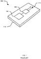
- FIG. 1 depicts a wireless communications assembly 100 according to the prior art.
- Assembly 100 includes a baseband processor 104 and a radio processor 108, as well as an antenna 112.
- the above-mentioned components are carried on a support 116 such as a printed circuit board (PCB).
- PCB printed circuit board
- the orientation of the components shown in FIG. 1 may vary, and although various other components (not shown) may also be included, all three of the baseband processor 104, radio processor 108 and antenna 112 are carried on the same support 116.
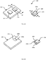
- Assembly 200 includes two physically distinct components: a first support member 204, which may also be referred to as a base board, and a second support member 208, which may also referred to as an antenna board.
- First support member 204 is, in the present embodiment, a printed circuit board (PCB) carrying a plurality of components and circuit geometries, including a baseband processor 212 and a radio processor 216.
- PCB printed circuit board
- a variety of other components may also be included within or on first support member 204, but are not directly relevant to the present discussion, and are therefore not illustrated for simplicity.
- Such components can include components supporting or otherwise directly associated with baseband processor 212 and radio processor 216.
- Such components can also include, in some embodiments, components not directly supporting or associated with those mentioned above (for example, baseband processor 212 and radio processor 216 can be components on a larger support member that fulfills a variety of functions beyond the wireless transmission and reception discussed herein).
- first support member 204 can be implemented as any suitable type of PCB, or indeed with any other suitable support materials and associated manufacturing processes.
- Processors 212 and 216 are connected to one another, for example via circuit traces in PCB 204 (not shown in FIG. 2A ).
- processor 212 and 216 are integrated circuits and can be mounted on PCB 204 by any suitable mechanism (e.g. ball grid array (BGA) and the like).
- BGA ball grid array
- processors 212 and 216 can be integrated with each other (that is, replaced by a single processor).
- Second support member 208 is also a PCB in the present embodiment.
- PCB 208 carries an antenna comprising a transmission element 220t and a reception element 220r (collectively referred to as antenna 220).
- Antenna 220 can have any of a wide variety of geometries in addition to that shown in FIG. 2A , and in the present example is constructed of circuit traces on a surface of PCB 208.
- radio processor 216 is an interface between baseband processor 212 and antenna 220. Thus, incoming signals are detected at antenna 220 and provided to radio processor 216 via structural elements to be discussed in greater detail below. Radio processor 216, in turn, generates processed signal data and transmits the data to baseband processor 212 for further processing. Baseband processor 212 can transmit further processed data to other components (not shown) via one or more interface components supported on PCB 204, such as a Universal Serial Bus (USB) port (not shown) connected to baseband processor 212.
- USB Universal Serial Bus
- baseband processor Based on data received, for example, via the above-mentioned interface component, baseband processor generates intermediate transmission data and provides the intermediate transmission data to radio processor 216. Radio processor 216, in turn, generates transmission data and controls antenna 220 (specifically, element 220t) to emit signals representing the transmission data.
- second support member 208 carries only antenna 220. That is, no other discrete components are carried by second support member 208, and second member 208 includes only those circuit traces required to implement antenna 220 and connect antenna 220 to first support member 204 via the structures to be described herein.
- second support member 208 can support components in addition to antenna 220.
- radio processor 216 and baseband processor 212 and their associated traces and components are supported not on second support member 208, but on first support member 204.
- processors 212 and 216 are carried by a support member separate and distinct from the support member carrying antenna 220.
- antenna 220 is connected to radio processor 216.
- radio processor 216 reside on separate support members
- support members 204 and 208 each include mounting structures for establishing the connection between antenna 220 and radio processor 216.
- support members 204 and 208 are shown as viewed from the sides opposite to those shown in FIG. 2A . That is, if the surfaces supporting processors 212 and 216, as well as antenna 220, are referred to as the "upper” surfaces of support members 204 and 208, FIG. 2B depicts the "lower” surfaces of support members 204 and 208.
- support member 204 defines a first mounting surface 224 (indicated by dashed lines) including a first pair of electrical contacts 228a and 228b (collectively referred to as electrical contacts 228).
- Mounting surface 224 can be, but is not necessarily, visually or physically demarcated on support member 204 (beyond the presence of electrical contacts 228).
- first mounting surface 224 lies substantially opposite radio processor 216 (that is, substantially underneath radio processor 216).
- Support member 208 defines a second mounting surface 232 (indicated by dashed lines) including a second pair of electrical contacts 236a and 236b (collectively referred to as electrical contacts 236).
- second mounting surface 232 can be but is not necessarily, visually or physically demarcated on support member 208.
- the presence of electrical contacts 236 is sufficient to indicate the position of second mounting surface 232 on support member 208.
- Each of support members 204 and 208 also includes electrical connections, as will be described below in connection with FIGS. 3A and 3B as well as FIGS. 4A and 4B .
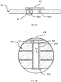
- FIG. 3A a cross-sectional view of first support member 204 taken from line 3A-3A in FIG. 2A is shown.
- Support member 204 includes a first pair of electrical connections 300a and 300b (collectively referred to as electrical connections 300) between radio processor 216 and first electrical contacts 228. More specifically, electrical connection 300a connects radio processor 216 with electrical contact 228a, and electrical connection 300b connects radio processor 216 with electrical contact 228b.
- electrical connections 300 are holes or vias extending through support member 204 from the side carrying radio processor 216 to the opposite side (that is, the side bearing first mounting surface 224).
- electrical connection 300b (the same features apply to electrical connection 300a) is a via drilled through first support member 204 and plated with a conductive material 304, such as copper. In the present embodiment, all vias are mechanically drilled. However, other processes may also be employed to create vias. The via may be filled with any of a variety of suitable materials (e.g. solder, epoxy and the like), but the filling is omitted from FIG. 3B for simplicity of illustration. Electrical connection 300b connects radio processor 216 to electrical contact 228b, which in the present embodiment is a conductive pad (e.g. of copper) on mounting surface 224. In other words, electrical connection 300b may be referred to as an "in pad" via.
- a conductive pad e.g. of copper
- Radio processor 216 is shown connected to connection 300b via a pad 308 and a solder ball 312, although a wide variety of surface mounting technologies other than BGA may also be employed to couple radio processor 216 to support member 204 (e.g. pin grid array (PGA), land grid array (LGA) and the like).
- PGA pin grid array
- LGA land grid array
- support member 204 is a four-layer board (e.g. consisting of two double-sided copper-plated core members laminated on either side of a non-conductive pre-preg member). As illustrated, the copper layers (which can include ground planes, circuit traces and the like) do not contact electrical connection 300b.
- second support member 208 includes a second pair of electrical connections 400a and 400b (collectively referred to as electrical connections 400) between antenna 220 and second electrical contacts 236. More specifically, electrical connection 400a connects antenna element 220r with electrical contact 236a, and electrical connection 400b connects antenna element 220t with electrical contact 236b.
- electrical connections 400 are holes or vias extending through support member 208 from the side carrying antenna 220 to the opposite side (that is, the side bearing second mounting surface 232).
- electrical connection 400a (connection 400b has the same features) comprises a hole drilled through second support member 208 and plated with a conductor 404 (e.g. copper).
- second support member 208 is a two-layer PCB, consisting of a single nonconductive layer with opposing surfaces thereof plated with conductive material such as copper.
- Antenna 220 can be etched from the conductive plating on one side of support member 208.
- Other manufacturing processes may also be employed to fabricate antenna 220 and the remainder of support member 208, including both subtractive processes such as etching (mentioned above) and additive processes.
- second support member 208 can include a greater number of conductive layers than two, and any of a variety of conventional support material constructions can be employed. For example, larger numbers of layers may be employed to support more complex antenna geometries. In such embodiments, connections 400 can traverse support member 208 without connecting to any intermediate conductive layers, as discussed above in connection with FIG. 3B .
- connection 400a which corresponds to connection 400a
- connection 400a is not shown in FIG. 4B .
- a variety of electrical contacts are contemplated.
- the via of connection 400a may be filled and copper (or other conductive material) may be plated over the end of the via to provide electrical contact 236a, similarly to the implementation shown in FIG. 3B .
- solder is employed to both fill the vias of electrical connections 400 and create electrical contacts 236.
- solder mask 500 is deposited around the openings of the vias, and a deposit 504 of solder paste is applied (e.g. by silk-screening) over the opening of the vias on the side of support member 208 defining mounting surface 232. Additional deposits 508 of solder paste may also be placed on ground pads.
- support member 208 is heated (e.g. via a reflow process). During the heating process, a portion of solder deposit 504 is drawn into the via of connection 400a, and the remainder forms a solder bump defining electrical connector 400a.
- the process described above simultaneously fills the via of connection 400a and forms a ball-grid array (BGA) mounting structure on mounting surface 232.
- BGA ball-grid array
- Other fabrication processes may also be employed to produce support member 208 (e.g. to via fill and plate). Such processes may be performed at PCB fabrication instead of at the assembly stage.
- Second mounting surface 232 is configured to engage with first mounting surface 224 to rigidly couple first support member 204 with second support member 208. Engagement of second mounting surface 232 with first mounting surface 224 also brings first electrical contacts 228 into contact with second electrical contacts 236 and thus electrically connects radio processor 216 with antenna 220. Specifically, receiving element 220r is connected to radio processor 216 via electrical connections 400a and 300a, while transmitting element 220t is connected to radio processor 216 via electrical connections 400b and 300b.
- first and second mounting surfaces 224 and 232 are dependent on the nature of the electrical contacts 228 and 236.
- contacts 228 are conductive pads and contacts 236 form a ball grid array
- engagement between first and second mounting surfaces 224 and 232 is provided by placing second support member 208 (either manually or via an automated placement tool) on first support member 204 such that the mounting surfaces 224 and 232 are aligned.
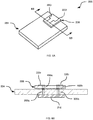
- FIGS. 6A and 6B depict assembly 200 in the assembled state, after first support member 204 and second support member 208 have been rigidly coupled.
- second support member 208 is coupled to first support member 204 such that radio processor 216 and second support member 208 lie on substantially opposite portions of first support member 204.
- electrical connections 300a and 400a are axially aligned and connected via electrical contacts 228a and 236a to connect antenna 220 with radio processor 216.
- Electrical connections 300b and 400b are similarly axially aligned and connected.
- second support member 208 can also be coupled to first support member via pin-based surface mount structures, including pin grid array (PGA), land grid array (LGA) and the like.
- castellation may be employed to connect first and second support members 204 and 208.
- an edge of second support member 208 is castellated such that electrical connections 400a and 400b are open channels defining castellations. The application of solder within the castellations after placement of second support member 208 on first support member 204 serves to couple the support members.
- second support member 208 can be removed from first support member 204, for example to permit a different antenna board to be employed on the same base board.
- the removal of second support member 208 is accomplished by heating assembly 200 to melt the solder balls, upon which the solder can be cleaned from first support member 204.
- FIGS. 7A and 7B depict other example form factors for assembly 200 are also contemplated.
- FIG. 7A depicts a first support member 704 coupled to a second support member 708 such that second support member 708 hangs over an edge of first support member 704.
- Radio processor 216 is placed on the opposite side of first support member 704 from second support member.
- FIG. 7B places a second support member 718 within the edges of a first support member 714; radio processor 216 is located accordingly, to remain opposite second support member 718.
- form factors can be employed to couple the antenna and base boards described herein.
- the physical separation of antenna 220 from the board carrying processors 212 and 216 may allow the base boards to be manufactured with relaxed tolerances, and may also allow less costly manufacturing for the antenna boards, as meeting required tolerances is less difficult when fewer components and circuit traces are present.
- the separation of boards as described above may also permit each board to be manufactured with a smaller number of layers than would be required to manufacture a single board carrying all components. Reducing the number of layers may reduce or eliminate the need for various processes that can introduce deviations from specified dimensions. For example, the need for laser drilling processes may be eliminated, allowing mechanical drilling to be employed for vias (which is generally less costly and produces vias with more consistent barrel dimensions).
- the design and prototyping cycle of each antenna design may be less costly and time-consuming, thus permitting a greater variety of antenna designs to be pursued with similar development resources.
- first support member 204 can include an internal layer reserved for an integrated antenna trace, and a blind via connecting radio processor 216 with that layer.
- the above-mentioned reserved layer and blind via can be included in addition to the electrical connections, mounting surfaces and contacts described above.
- a single base board design can be used in conjunction with physically separate antennas (i.e. on second support member 208), but is also amenable to incorporating a selected antenna design on the reserved layer, without requiring relocation of the other components of the base board.
- a single first support member can carry a plurality of second support members (i.e. a plurality of antennas).
- a first support member each carrying respective radio and baseband processors can carry a single second support member (i.e. a single antenna). More generally, the ratio between first and second support members need not be one-to-one.
- baseband processor 212 need not be located on the same support member as radio processor 216. For example, in some embodiments, baseband processor 212 can be located on a further support member that is electrically connected to first support member 204.
Landscapes
- Physics & Mathematics (AREA)
- Engineering & Computer Science (AREA)
- Electromagnetism (AREA)
- Computer Networks & Wireless Communication (AREA)
- Signal Processing (AREA)
- General Physics & Mathematics (AREA)
- Microelectronics & Electronic Packaging (AREA)
- Support Of Aerials (AREA)
- Details Of Aerials (AREA)
Description
- The specification relates generally to wireless communications, and specifically to a wireless communications assembly and a method of testing prototype antennas for the wireless communications assembly.
- The performance of wireless antennas (e.g. antenna, dielectric and via geometries in or on printed circuit board assemblies) is known to be dependent on the precision of these geometries. Particularly at higher frequencies - such as those employed by the IEEE 802.11 ad standard (also referred to as WiGig), which employs the 60GHz frequency band - sensitivity of antenna performance to geometry can be very pronounced. As a result, antennas for use in high-frequency applications are often produced with strict manufacturing tolerances. Adhering to such strict design tolerance requirements, however, increase the difficulty (and therefore the cost and time) of production.
- In addition to the challenges posed by strict manufacturing tolerances, the complexity required to successfully design, simulate, prototype, and validate high-frequency antennas into productions limits the number of viable antenna solutions that can be produced because of the cost and time associated with the above-mentioned design cycle, particularly when the cycle is repeated to refine the design. This cycle can limit the pace at which new antennas can be developed to meet different high-frequency antenna requirements.
- A further complicating factor in the production of wireless radio assemblies for high-frequency applications is the issue of signal attenuation between the antenna and processing circuitry: leads between antenna and processors are generally kept as short as possible to reduce signal losses. Together, the above-mentioned challenges tend to increase the complexity and cost of manufacturing high-frequency wireless communication assemblies.
-
US2014/0138804 describes a semiconductor component face-up mounted on a package substrate. An antenna substrate is flip-chip mounted on a front side of the semiconductor component. -
WO2015/088486 describes an antenna on ceramics used for a packaged die. In one example, a package has a die, a ceramic substrate over the die, an antenna attached to the ceramic substrate, and conductive leads electrically connecting the antenna to the die. - According to an aspect of the invention, a wireless communication assembly is provided in independent claim 1.
- According to a further aspect of the invention, a method of testing prototype antennas for the wireless communications assembly is provided in independent claim 13.
- Optional features are set out in the dependent claims.
- Embodiments are described with reference to the following figures, in which:
-
FIG. 1 depicts a wireless communications assembly, according to the prior art; -
FIGS. 2A and 2B depict opposing sides of two support members of a wireless communication assembly, according to a non-limiting embodiment; -
FIG. 3A depicts a cross section of the first support member ofFIGS. 2A and 2B , according to a non-limiting embodiment; -
FIG. 3B depicts a detailed cross section of the portion of the first support member identified inFIG. 3A , according to a non-limiting embodiment; -
FIG. 4A depicts a cross section of the second support member ofFIGS. 2A and 2B , according to a non-limiting embodiment; -
FIG. 4B depicts a detailed cross section of the portion of the second support member identified inFIG. 4A , according to a non-limiting embodiment; -
FIGS. 5A and 5B depict detailed cross sections of the portion of the second support member identified inFIG. 4A during manufacturing/assembly, according to a non-limiting embodiment; -
FIG. 6A depicts the wireless communication assembly ofFIGS. 2A and 2B in an assembled state, according to a non-limiting embodiment -
FIG. 6B depicts a cross section of the wireless communication assembly ofFIG. 6A , according to a non-limiting embodiment; and -
FIGS. 7A and 7B depict alternative form factors for the wireless communication assembly ofFIGS. 2A and 2B , according to a non-limiting embodiment. -
FIG. 1 depicts awireless communications assembly 100 according to the prior art.Assembly 100 includes abaseband processor 104 and aradio processor 108, as well as anantenna 112. The above-mentioned components are carried on asupport 116 such as a printed circuit board (PCB). In general, although the orientation of the components shown inFIG. 1 may vary, and although various other components (not shown) may also be included, all three of thebaseband processor 104,radio processor 108 andantenna 112 are carried on thesame support 116. - Turning now to
FIG. 2A , a wireless communications assembly 200 (also referred to herein simply as "assembly 200") according to embodiments of the present invention is illustrated.Assembly 200 includes two physically distinct components: afirst support member 204, which may also be referred to as a base board, and asecond support member 208, which may also referred to as an antenna board. -
First support member 204 is, in the present embodiment, a printed circuit board (PCB) carrying a plurality of components and circuit geometries, including abaseband processor 212 and aradio processor 216. A variety of other components may also be included within or onfirst support member 204, but are not directly relevant to the present discussion, and are therefore not illustrated for simplicity. Such components can include components supporting or otherwise directly associated withbaseband processor 212 andradio processor 216. Such components can also include, in some embodiments, components not directly supporting or associated with those mentioned above (for example,baseband processor 212 andradio processor 216 can be components on a larger support member that fulfills a variety of functions beyond the wireless transmission and reception discussed herein). Further, as will now be apparent to those skilled in the art,first support member 204 can be implemented as any suitable type of PCB, or indeed with any other suitable support materials and associated manufacturing processes.Processors FIG. 2A ). In the present example,processor PCB 204 by any suitable mechanism (e.g. ball grid array (BGA) and the like). In some embodiments,processors -
Second support member 208 is also a PCB in the present embodiment.PCB 208 carries an antenna comprising atransmission element 220t and areception element 220r (collectively referred to as antenna 220). Antenna 220 can have any of a wide variety of geometries in addition to that shown inFIG. 2A , and in the present example is constructed of circuit traces on a surface ofPCB 208. - In general,
radio processor 216 is an interface betweenbaseband processor 212 and antenna 220. Thus, incoming signals are detected at antenna 220 and provided toradio processor 216 via structural elements to be discussed in greater detail below.Radio processor 216, in turn, generates processed signal data and transmits the data to basebandprocessor 212 for further processing.Baseband processor 212 can transmit further processed data to other components (not shown) via one or more interface components supported onPCB 204, such as a Universal Serial Bus (USB) port (not shown) connected tobaseband processor 212. - Outgoing signals, meanwhile, follow the reverse of the path described above: based on data received, for example, via the above-mentioned interface component, baseband processor generates intermediate transmission data and provides the intermediate transmission data to
radio processor 216.Radio processor 216, in turn, generates transmission data and controls antenna 220 (specifically,element 220t) to emit signals representing the transmission data. - As shown in
FIG. 2A , in the present embodiment,second support member 208 carries only antenna 220. That is, no other discrete components are carried bysecond support member 208, andsecond member 208 includes only those circuit traces required to implement antenna 220 and connect antenna 220 tofirst support member 204 via the structures to be described herein. - In other embodiments,
second support member 208 can support components in addition to antenna 220. However, it is contemplated that even in such other embodiments,radio processor 216 andbaseband processor 212 and their associated traces and components are supported not onsecond support member 208, but onfirst support member 204. In other words, it is contemplated thatprocessors - It will now be apparent to those skilled in the art that in operation, antenna 220 is connected to
radio processor 216. Given that antenna 220 andradio processor 216 reside on separate support members,support members radio processor 216. - Referring now to
FIG. 2B ,support members FIG. 2A . That is, if thesurfaces supporting processors support members FIG. 2B depicts the "lower" surfaces ofsupport members - As seen in
FIG. 2B ,support member 204 defines a first mounting surface 224 (indicated by dashed lines) including a first pair ofelectrical contacts surface 224 can be, but is not necessarily, visually or physically demarcated on support member 204 (beyond the presence of electrical contacts 228). As seen fromFIGS. 2A and 2B , first mountingsurface 224 lies substantially opposite radio processor 216 (that is, substantially underneath radio processor 216). -
Support member 208 defines a second mounting surface 232 (indicated by dashed lines) including a second pair ofelectrical contacts surface 224, second mountingsurface 232 can be but is not necessarily, visually or physically demarcated onsupport member 208. In some embodiments, the presence of electrical contacts 236 is sufficient to indicate the position of second mountingsurface 232 onsupport member 208. - Each of
support members FIGS. 3A and 3B as well asFIGS. 4A and 4B . Referring first toFIG. 3A , a cross-sectional view offirst support member 204 taken fromline 3A-3A inFIG. 2A is shown.Support member 204 includes a first pair ofelectrical connections radio processor 216 and first electrical contacts 228. More specifically,electrical connection 300a connectsradio processor 216 withelectrical contact 228a, andelectrical connection 300b connectsradio processor 216 withelectrical contact 228b. In the present embodiment, electrical connections 300 are holes or vias extending throughsupport member 204 from the side carryingradio processor 216 to the opposite side (that is, the side bearing first mounting surface 224). - Referring to the detail view shown in
FIG. 3B ,electrical connection 300b (the same features apply toelectrical connection 300a) is a via drilled throughfirst support member 204 and plated with aconductive material 304, such as copper. In the present embodiment, all vias are mechanically drilled. However, other processes may also be employed to create vias. The via may be filled with any of a variety of suitable materials (e.g. solder, epoxy and the like), but the filling is omitted fromFIG. 3B for simplicity of illustration.Electrical connection 300b connectsradio processor 216 toelectrical contact 228b, which in the present embodiment is a conductive pad (e.g. of copper) on mountingsurface 224. In other words,electrical connection 300b may be referred to as an "in pad" via.Radio processor 216 is shown connected toconnection 300b via apad 308 and asolder ball 312, although a wide variety of surface mounting technologies other than BGA may also be employed to coupleradio processor 216 to support member 204 (e.g. pin grid array (PGA), land grid array (LGA) and the like). - It is also contemplated that
electrical connection 300b traversessupport member 204 without electrically connecting to any other components ofsupport member 204. For example, as shown inFIG. 3B ,support member 204 is a four-layer board (e.g. consisting of two double-sided copper-plated core members laminated on either side of a non-conductive pre-preg member). As illustrated, the copper layers (which can include ground planes, circuit traces and the like) do not contactelectrical connection 300b. - Turning now to
FIG. 4A , a cross section ofsecond support member 208, taken atline 4A-4A labelled inFIG. 2A , is illustrated. As seen inFIG. 4A ,second support member 208 includes a second pair ofelectrical connections electrical connection 400a connectsantenna element 220r withelectrical contact 236a, andelectrical connection 400b connectsantenna element 220t withelectrical contact 236b. - In the present embodiment, electrical connections 400 are holes or vias extending through
support member 208 from the side carrying antenna 220 to the opposite side (that is, the side bearing second mounting surface 232). As shown in the detail view ofFIG. 4B ,electrical connection 400a (connection 400b has the same features) comprises a hole drilled throughsecond support member 208 and plated with a conductor 404 (e.g. copper). As seen inFIG. 4B ,second support member 208 is a two-layer PCB, consisting of a single nonconductive layer with opposing surfaces thereof plated with conductive material such as copper. Antenna 220 can be etched from the conductive plating on one side ofsupport member 208. Other manufacturing processes may also be employed to fabricate antenna 220 and the remainder ofsupport member 208, including both subtractive processes such as etching (mentioned above) and additive processes. - In other embodiments,
second support member 208 can include a greater number of conductive layers than two, and any of a variety of conventional support material constructions can be employed. For example, larger numbers of layers may be employed to support more complex antenna geometries. In such embodiments, connections 400 can traversesupport member 208 without connecting to any intermediate conductive layers, as discussed above in connection withFIG. 3B . - It will be noted that
electrical contact 236a, which corresponds toconnection 400a, is not shown inFIG. 4B . A variety of electrical contacts are contemplated. In some embodiments the via ofconnection 400a may be filled and copper (or other conductive material) may be plated over the end of the via to provideelectrical contact 236a, similarly to the implementation shown inFIG. 3B . In the present embodiment, however, as shown inFIGS. 5A and 5B , solder is employed to both fill the vias of electrical connections 400 and create electrical contacts 236. - As shown in
FIG. 5A , after the vias for connections 400 have been drilled and plated,solder mask 500 is deposited around the openings of the vias, and adeposit 504 of solder paste is applied (e.g. by silk-screening) over the opening of the vias on the side ofsupport member 208 defining mountingsurface 232.Additional deposits 508 of solder paste may also be placed on ground pads. Following the application ofsolder paste deposits support member 208 is heated (e.g. via a reflow process). During the heating process, a portion ofsolder deposit 504 is drawn into the via ofconnection 400a, and the remainder forms a solder bump definingelectrical connector 400a.Deposits 508, after reflow treatment, also form solder bumps 516 over the above-mentioned ground pads. In other words, the process described above simultaneously fills the via ofconnection 400a and forms a ball-grid array (BGA) mounting structure on mountingsurface 232. Other fabrication processes may also be employed to produce support member 208 (e.g. to via fill and plate). Such processes may be performed at PCB fabrication instead of at the assembly stage. - Second mounting
surface 232 is configured to engage with first mountingsurface 224 to rigidly couplefirst support member 204 withsecond support member 208. Engagement of second mountingsurface 232 with first mountingsurface 224 also brings first electrical contacts 228 into contact with second electrical contacts 236 and thus electrically connectsradio processor 216 with antenna 220. Specifically, receivingelement 220r is connected toradio processor 216 viaelectrical connections element 220t is connected toradio processor 216 viaelectrical connections - As will now be apparent to those skilled in the art, the mechanism of engagement between first and second mounting surfaces 224 and 232 is dependent on the nature of the electrical contacts 228 and 236. In the embodiments described above, in which contacts 228 are conductive pads and contacts 236 form a ball grid array, engagement between first and second mounting surfaces 224 and 232 is provided by placing second support member 208 (either manually or via an automated placement tool) on
first support member 204 such that the mountingsurfaces - Following placement of
second support member 208 onfirst support member 204, the assembled support members are subjected to a reflow operation to melt the solder balls on second support member 208 (shown inFIG. 5B ) and fixsecond support member 208 tofirst support member 204.FIGS. 6A and 6B depict assembly 200 in the assembled state, afterfirst support member 204 andsecond support member 208 have been rigidly coupled. As best seen inFIG. 6B ,second support member 208 is coupled tofirst support member 204 such thatradio processor 216 andsecond support member 208 lie on substantially opposite portions offirst support member 204. More specifically,electrical connections electrical contacts radio processor 216.Electrical connections - Various other mechanisms for rigidly coupling first and
second support members second support member 208 can also be coupled to first support member via pin-based surface mount structures, including pin grid array (PGA), land grid array (LGA) and the like. In other embodiments, castellation may be employed to connect first andsecond support members second support member 208 is castellated such thatelectrical connections second support member 208 onfirst support member 204 serves to couple the support members. - In some embodiments, including the BGA-based embodiments discussed above,
second support member 208 can be removed fromfirst support member 204, for example to permit a different antenna board to be employed on the same base board. When the coupling betweensupport members second support member 208 is accomplished byheating assembly 200 to melt the solder balls, upon which the solder can be cleaned fromfirst support member 204. - Turning now to
FIGS. 7A and 7B , other example form factors forassembly 200 are also contemplated. Each ofFIG. 7A and 7B depicts opposing sides of an example variation ofassembly 200.FIG. 7A , for example, depicts afirst support member 704 coupled to asecond support member 708 such thatsecond support member 708 hangs over an edge offirst support member 704.Radio processor 216 is placed on the opposite side offirst support member 704 from second support member. The example ofFIG. 7B , in contrast, places asecond support member 718 within the edges of afirst support member 714;radio processor 216 is located accordingly, to remain oppositesecond support member 718. In general, it will now be apparent to those skilled in the art that a wide variety of form factors can be employed to couple the antenna and base boards described herein. - Various advantages to the assemblies described above will now be apparent to those skilled in the art. For example, the physical separation of antenna 220 from the
board carrying processors - Variations to the above are also contemplated, beyond those variations already mentioned. For example, in some embodiments,
first support member 204 can include an internal layer reserved for an integrated antenna trace, and a blind via connectingradio processor 216 with that layer. The above-mentioned reserved layer and blind via can be included in addition to the electrical connections, mounting surfaces and contacts described above. Thus, a single base board design can be used in conjunction with physically separate antennas (i.e. on second support member 208), but is also amenable to incorporating a selected antenna design on the reserved layer, without requiring relocation of the other components of the base board. - In further variations, a single first support member can carry a plurality of second support members (i.e. a plurality of antennas). In still further variations, a first support member each carrying respective radio and baseband processors (or multiple first support members each carrying a radio and baseband processor) can carry a single second support member (i.e. a single antenna). More generally, the ratio between first and second support members need not be one-to-one. In still further variations,
baseband processor 212 need not be located on the same support member asradio processor 216. For example, in some embodiments,baseband processor 212 can be located on a further support member that is electrically connected tofirst support member 204. - Other variations will also occur to those skilled in the art in light of the above description. The scope of the claims should not be limited by the embodiments set forth in the above examples, but should be given the broadest interpretation consistent with the description as a whole.
Claims (11)
- A wireless communication assembly (200), comprising:a first support member (204) carrying a baseband processor (212) and a radio processor (216) connected to the baseband processor (212); the first support member (204) defining a first mounting surface (224) including a first pair of electrical contacts (228);the first support member (204) having a first pair of electrical connections (300) between the radio processor (216) and the first pair of electrical contacts (228); anda second support member (208) carrying an antenna (220) and defining a second mounting surface (232) including a second pair of electrical contacts (236); the second support member (208) having a second pair of electrical connections (400) between the antenna (220) and the second pair of electrical contacts (236);the second mounting surface (232) configured to engage with the first mounting surface (224) to rigidly couple the first and second support members (204, 208) and to bring the first pair of electrical contacts (228) into contact with the second pair of electrical contacts (236) for electrically connecting the radio processor (216) and the antenna (220) via the first and second pairs of electrical connections (300, 400), wherein the radio processor (216) is carried on a side of the first support member (204) opposite the first mounting surface (224) and wherein the antenna (220) is carried on a side of the second support member (208) opposite the second mounting surface (232).
- The wireless communication assembly (200) of claim 1, the first pair of electrical connections (300) comprising vias extending through the first support member (204), from the side of the first support member (204) carrying the radio processor (216) to the first mounting surface (224).
- The wireless communication assembly (200) of claim 1, the second pair of electrical connections (400) comprising vias extending through the second support member (208), from the side of the second support member (208) carrying the antenna (220) to the second mounting surface (232).
- The wireless communication assembly (200) of claim 3, wherein the vias are orthogonal to the side of the second support member (208) carrying the antenna (220).
- The wireless communication assembly (200) of claim 4, the second pair of electrical contacts (236) comprising solder bumps forming a ball grid array (BGA).
- The wireless communications assembly (200) of claim 1, wherein:the second support member (208) is an antenna support member; andthe first support member (204) comprises a base component of the wireless communications assembly (200); andthe first mounting surface comprises a corresponding mounting surface of the base component of the wireless communications assembly.
- The wireless communications assembly (200) of claim 6, the second pair of electrical connections (400) comprising vias extending through the antenna support member (208), from the side of the antenna support member (208) carrying the antenna (220) to the second mounting surface (232).
- The wireless communications assembly (200) of claim 7, the second pair of electrical contacts (236) comprising solder bumps forming a ball grid array (BGA).
- The wireless communications assembly of claim 1, wherein:the first support member (204) is a base support member (204);the second support member comprises an antenna component of the wireless communications assembly comprising the antenna; andthe second mounting surface comprises a corresponding mounting surface of the antenna component of the wireless communications assembly.
- The wireless communications assembly (200) of claim 9 the first pair of electrical connections (300) comprising vias extending through the base support member (204), from the side of the base support member (204) carrying the radio processor (216) to the first mounting surface (224).
- A method of testing prototype antennas (220) for a wireless communications assembly (200) according to any of claims 1 to 10 the method comprising:selecting a first support member (204) carrying a baseband processor (212) and a radio processor (216) connected to the baseband processor (212);selecting a second support member (208) carrying an antenna (220);aligning respective mounting surfaces (224, 232) of the first support member (204) and the second support member (208);mounting the second mounting surface (232) to the first mounting surface (224) to electrically connect the antenna (220) with the radio processor (216);applying a signal to the antenna (220);decoupling the second support member (208) from the first support member (204); andrepeating the selecting a second support member (208), the aligning, the mounting and the applying, wherein the radio processor (216) is carried on a side of the first support member (204) opposite the mounting surface (224) of the first support member (204) and wherein the antenna (220) is carried on a side of the second support member (208) opposite the second mounting surface (232).
Applications Claiming Priority (1)
| Application Number | Priority Date | Filing Date | Title |
|---|---|---|---|
| US15/010,465 US9961774B2 (en) | 2016-01-29 | 2016-01-29 | Wireless communications assembly |
Publications (2)
| Publication Number | Publication Date |
|---|---|
| EP3200277A1 EP3200277A1 (en) | 2017-08-02 |
| EP3200277B1 true EP3200277B1 (en) | 2020-09-02 |
Family
ID=57914900
Family Applications (1)
| Application Number | Title | Priority Date | Filing Date |
|---|---|---|---|
| EP17153770.7A Active EP3200277B1 (en) | 2016-01-29 | 2017-01-30 | Wireless communications assembly |
Country Status (3)
| Country | Link |
|---|---|
| US (1) | US9961774B2 (en) |
| EP (1) | EP3200277B1 (en) |
| CN (1) | CN107026666B (en) |
Families Citing this family (1)
| Publication number | Priority date | Publication date | Assignee | Title |
|---|---|---|---|---|
| US10320131B2 (en) * | 2017-06-20 | 2019-06-11 | Microsoft Technology Licensing, Llc | Recessed switched test connector |
Family Cites Families (8)
| Publication number | Priority date | Publication date | Assignee | Title |
|---|---|---|---|---|
| EP1413004A4 (en) * | 2001-05-17 | 2004-07-21 | Cypress Semiconductor Corp | BALL MATRIX GRID ANTENNA |
| US7262735B2 (en) | 2004-11-29 | 2007-08-28 | Lexmark International, Inc. | Snap-in antenna assembly for wireless radio circuit card |
| US8120173B2 (en) * | 2005-05-03 | 2012-02-21 | Lockheed Martin Corporation | Thin embedded active IC circuit integration techniques for flexible and rigid circuits |
| US20080122726A1 (en) * | 2006-11-27 | 2008-05-29 | Gil Levi | Low cost chip package with integrated RFantenna |
| US8013784B2 (en) * | 2009-03-03 | 2011-09-06 | Toyota Motor Engineering & Manufacturing North America, Inc. | Butler matrix for 3D integrated RF front-ends |
| US8213982B2 (en) * | 2009-06-01 | 2012-07-03 | Hewlett-Packard Development Company, L.P. | Enhanced internal antenna architecture for a mobile computing device |
| CN103026487A (en) | 2010-07-29 | 2013-04-03 | 株式会社村田制作所 | High frequency module and communication device |
| KR101833154B1 (en) * | 2013-12-09 | 2018-04-13 | 인텔 코포레이션 | Antenna on ceramics for a packaged die |
-
2016
- 2016-01-29 US US15/010,465 patent/US9961774B2/en active Active
-
2017
- 2017-01-26 CN CN201710191019.2A patent/CN107026666B/en active Active
- 2017-01-30 EP EP17153770.7A patent/EP3200277B1/en active Active
Non-Patent Citations (1)
| Title |
|---|
| None * |
Also Published As
| Publication number | Publication date |
|---|---|
| US9961774B2 (en) | 2018-05-01 |
| EP3200277A1 (en) | 2017-08-02 |
| US20170223831A1 (en) | 2017-08-03 |
| CN107026666B (en) | 2020-08-04 |
| CN107026666A (en) | 2017-08-08 |
Similar Documents
| Publication | Publication Date | Title |
|---|---|---|
| US11800636B2 (en) | Electronic substrate having differential coaxial vias | |
| KR102443287B1 (en) | Snap-to-RF interconnect | |
| US5459287A (en) | Socketed printed circuit board BGA connection apparatus and associated methods | |
| KR101702717B1 (en) | System and method for a millimeter wave circuit board | |
| EP1387403A2 (en) | Semiconductor packaging | |
| CN106935572B (en) | Methods to improve BGA package isolation in RF and mmWave products | |
| JP2005044779A (en) | Bonding technique for interbonding multilayer circuit board | |
| US20150282317A1 (en) | Edge contacts of circuit boards, and related apparatus and methods | |
| TW202044677A (en) | Electronic component mounting structure and method | |
| CN101142860A (en) | printed circuit board | |
| CN110139476B (en) | PCB module on package | |
| JP7291292B2 (en) | Additive manufacturing technology (AMT) inverted pad interface | |
| KR20200003113A (en) | PCB, package structure, terminal and PCB processing method | |
| KR101565690B1 (en) | Circuit board, method for menufacturing of circuit board, electronic component package and method for menufacturing of electronic component package | |
| US11581652B2 (en) | Spiral antenna and related fabrication techniques | |
| KR20210151967A (en) | Flat-Wire Copper Vertical Launch Microwave Interconnection Method | |
| TW201427523A (en) | Chip package structure, circuit board with embedded components and manufacturing method thereof | |
| EP3200277A1 (en) | Wireless communications assembly | |
| US20100289155A1 (en) | Semiconductor package | |
| JP2007227924A (en) | Circuit assembly and method for manufacturing electronic assembly | |
| CN103545303A (en) | IC package and assembly | |
| US7135764B2 (en) | Shielded semiconductor chip carrier having a high-density external interface | |
| KR20110131047A (en) | Embedded Printed Circuit Board Manufacturing Method and Embedded Printed Circuit Board Manufacturing Structure |
Legal Events
| Date | Code | Title | Description |
|---|---|---|---|
| PUAI | Public reference made under article 153(3) epc to a published international application that has entered the european phase |
Free format text: ORIGINAL CODE: 0009012 |
|
| STAA | Information on the status of an ep patent application or granted ep patent |
Free format text: STATUS: REQUEST FOR EXAMINATION WAS MADE |
|
| 17P | Request for examination filed |
Effective date: 20170130 |
|
| AK | Designated contracting states |
Kind code of ref document: A1 Designated state(s): AL AT BE BG CH CY CZ DE DK EE ES FI FR GB GR HR HU IE IS IT LI LT LU LV MC MK MT NL NO PL PT RO RS SE SI SK SM TR |
|
| AX | Request for extension of the european patent |
Extension state: BA ME |
|
| RIC1 | Information provided on ipc code assigned before grant |
Ipc: H01Q 1/38 20060101AFI20200204BHEP Ipc: H05K 1/14 20060101ALN20200204BHEP Ipc: H01Q 1/12 20060101ALI20200204BHEP Ipc: H04B 17/17 20150101ALI20200204BHEP |
|
| GRAP | Despatch of communication of intention to grant a patent |
Free format text: ORIGINAL CODE: EPIDOSNIGR1 |
|
| STAA | Information on the status of an ep patent application or granted ep patent |
Free format text: STATUS: GRANT OF PATENT IS INTENDED |
|
| RIC1 | Information provided on ipc code assigned before grant |
Ipc: H04B 17/17 20150101ALI20200210BHEP Ipc: H05K 1/14 20060101ALN20200210BHEP Ipc: H01Q 1/12 20060101ALI20200210BHEP Ipc: H01Q 1/38 20060101AFI20200210BHEP |
|
| RIC1 | Information provided on ipc code assigned before grant |
Ipc: H05K 1/14 20060101ALN20200219BHEP Ipc: H04B 17/17 20150101ALI20200219BHEP Ipc: H01Q 1/12 20060101ALI20200219BHEP Ipc: H01Q 1/38 20060101AFI20200219BHEP |
|
| INTG | Intention to grant announced |
Effective date: 20200313 |
|
| GRAS | Grant fee paid |
Free format text: ORIGINAL CODE: EPIDOSNIGR3 |
|
| GRAA | (expected) grant |
Free format text: ORIGINAL CODE: 0009210 |
|
| STAA | Information on the status of an ep patent application or granted ep patent |
Free format text: STATUS: THE PATENT HAS BEEN GRANTED |
|
| AK | Designated contracting states |
Kind code of ref document: B1 Designated state(s): AL AT BE BG CH CY CZ DE DK EE ES FI FR GB GR HR HU IE IS IT LI LT LU LV MC MK MT NL NO PL PT RO RS SE SI SK SM TR |
|
| REG | Reference to a national code |
Ref country code: GB Ref legal event code: FG4D |
|
| REG | Reference to a national code |
Ref country code: AT Ref legal event code: REF Ref document number: 1309873 Country of ref document: AT Kind code of ref document: T Effective date: 20200915 Ref country code: CH Ref legal event code: EP |
|
| REG | Reference to a national code |
Ref country code: DE Ref legal event code: R096 Ref document number: 602017022590 Country of ref document: DE |
|
| REG | Reference to a national code |
Ref country code: IE Ref legal event code: FG4D |
|
| REG | Reference to a national code |
Ref country code: LT Ref legal event code: MG4D |
|
| PG25 | Lapsed in a contracting state [announced via postgrant information from national office to epo] |
Ref country code: BG Free format text: LAPSE BECAUSE OF FAILURE TO SUBMIT A TRANSLATION OF THE DESCRIPTION OR TO PAY THE FEE WITHIN THE PRESCRIBED TIME-LIMIT Effective date: 20201202 Ref country code: NO Free format text: LAPSE BECAUSE OF FAILURE TO SUBMIT A TRANSLATION OF THE DESCRIPTION OR TO PAY THE FEE WITHIN THE PRESCRIBED TIME-LIMIT Effective date: 20201202 Ref country code: GR Free format text: LAPSE BECAUSE OF FAILURE TO SUBMIT A TRANSLATION OF THE DESCRIPTION OR TO PAY THE FEE WITHIN THE PRESCRIBED TIME-LIMIT Effective date: 20201203 Ref country code: SE Free format text: LAPSE BECAUSE OF FAILURE TO SUBMIT A TRANSLATION OF THE DESCRIPTION OR TO PAY THE FEE WITHIN THE PRESCRIBED TIME-LIMIT Effective date: 20200902 Ref country code: HR Free format text: LAPSE BECAUSE OF FAILURE TO SUBMIT A TRANSLATION OF THE DESCRIPTION OR TO PAY THE FEE WITHIN THE PRESCRIBED TIME-LIMIT Effective date: 20200902 Ref country code: LT Free format text: LAPSE BECAUSE OF FAILURE TO SUBMIT A TRANSLATION OF THE DESCRIPTION OR TO PAY THE FEE WITHIN THE PRESCRIBED TIME-LIMIT Effective date: 20200902 Ref country code: FI Free format text: LAPSE BECAUSE OF FAILURE TO SUBMIT A TRANSLATION OF THE DESCRIPTION OR TO PAY THE FEE WITHIN THE PRESCRIBED TIME-LIMIT Effective date: 20200902 |
|
| REG | Reference to a national code |
Ref country code: NL Ref legal event code: MP Effective date: 20200902 |
|
| REG | Reference to a national code |
Ref country code: AT Ref legal event code: MK05 Ref document number: 1309873 Country of ref document: AT Kind code of ref document: T Effective date: 20200902 |
|
| PG25 | Lapsed in a contracting state [announced via postgrant information from national office to epo] |
Ref country code: LV Free format text: LAPSE BECAUSE OF FAILURE TO SUBMIT A TRANSLATION OF THE DESCRIPTION OR TO PAY THE FEE WITHIN THE PRESCRIBED TIME-LIMIT Effective date: 20200902 Ref country code: RS Free format text: LAPSE BECAUSE OF FAILURE TO SUBMIT A TRANSLATION OF THE DESCRIPTION OR TO PAY THE FEE WITHIN THE PRESCRIBED TIME-LIMIT Effective date: 20200902 Ref country code: PL Free format text: LAPSE BECAUSE OF FAILURE TO SUBMIT A TRANSLATION OF THE DESCRIPTION OR TO PAY THE FEE WITHIN THE PRESCRIBED TIME-LIMIT Effective date: 20200902 |
|
| PG25 | Lapsed in a contracting state [announced via postgrant information from national office to epo] |
Ref country code: CZ Free format text: LAPSE BECAUSE OF FAILURE TO SUBMIT A TRANSLATION OF THE DESCRIPTION OR TO PAY THE FEE WITHIN THE PRESCRIBED TIME-LIMIT Effective date: 20200902 Ref country code: RO Free format text: LAPSE BECAUSE OF FAILURE TO SUBMIT A TRANSLATION OF THE DESCRIPTION OR TO PAY THE FEE WITHIN THE PRESCRIBED TIME-LIMIT Effective date: 20200902 Ref country code: PT Free format text: LAPSE BECAUSE OF FAILURE TO SUBMIT A TRANSLATION OF THE DESCRIPTION OR TO PAY THE FEE WITHIN THE PRESCRIBED TIME-LIMIT Effective date: 20210104 Ref country code: EE Free format text: LAPSE BECAUSE OF FAILURE TO SUBMIT A TRANSLATION OF THE DESCRIPTION OR TO PAY THE FEE WITHIN THE PRESCRIBED TIME-LIMIT Effective date: 20200902 Ref country code: SM Free format text: LAPSE BECAUSE OF FAILURE TO SUBMIT A TRANSLATION OF THE DESCRIPTION OR TO PAY THE FEE WITHIN THE PRESCRIBED TIME-LIMIT Effective date: 20200902 |
|
| PG25 | Lapsed in a contracting state [announced via postgrant information from national office to epo] |
Ref country code: IS Free format text: LAPSE BECAUSE OF FAILURE TO SUBMIT A TRANSLATION OF THE DESCRIPTION OR TO PAY THE FEE WITHIN THE PRESCRIBED TIME-LIMIT Effective date: 20210102 Ref country code: ES Free format text: LAPSE BECAUSE OF FAILURE TO SUBMIT A TRANSLATION OF THE DESCRIPTION OR TO PAY THE FEE WITHIN THE PRESCRIBED TIME-LIMIT Effective date: 20200902 Ref country code: AT Free format text: LAPSE BECAUSE OF FAILURE TO SUBMIT A TRANSLATION OF THE DESCRIPTION OR TO PAY THE FEE WITHIN THE PRESCRIBED TIME-LIMIT Effective date: 20200902 Ref country code: AL Free format text: LAPSE BECAUSE OF FAILURE TO SUBMIT A TRANSLATION OF THE DESCRIPTION OR TO PAY THE FEE WITHIN THE PRESCRIBED TIME-LIMIT Effective date: 20200902 |
|
| REG | Reference to a national code |
Ref country code: DE Ref legal event code: R097 Ref document number: 602017022590 Country of ref document: DE |
|
| PG25 | Lapsed in a contracting state [announced via postgrant information from national office to epo] |
Ref country code: SK Free format text: LAPSE BECAUSE OF FAILURE TO SUBMIT A TRANSLATION OF THE DESCRIPTION OR TO PAY THE FEE WITHIN THE PRESCRIBED TIME-LIMIT Effective date: 20200902 |
|
| PLBE | No opposition filed within time limit |
Free format text: ORIGINAL CODE: 0009261 |
|
| STAA | Information on the status of an ep patent application or granted ep patent |
Free format text: STATUS: NO OPPOSITION FILED WITHIN TIME LIMIT |
|
| 26N | No opposition filed |
Effective date: 20210603 |
|
| PG25 | Lapsed in a contracting state [announced via postgrant information from national office to epo] |
Ref country code: DK Free format text: LAPSE BECAUSE OF FAILURE TO SUBMIT A TRANSLATION OF THE DESCRIPTION OR TO PAY THE FEE WITHIN THE PRESCRIBED TIME-LIMIT Effective date: 20200902 Ref country code: SI Free format text: LAPSE BECAUSE OF FAILURE TO SUBMIT A TRANSLATION OF THE DESCRIPTION OR TO PAY THE FEE WITHIN THE PRESCRIBED TIME-LIMIT Effective date: 20200902 Ref country code: MC Free format text: LAPSE BECAUSE OF FAILURE TO SUBMIT A TRANSLATION OF THE DESCRIPTION OR TO PAY THE FEE WITHIN THE PRESCRIBED TIME-LIMIT Effective date: 20200902 |
|
| REG | Reference to a national code |
Ref country code: CH Ref legal event code: PL |
|
| PG25 | Lapsed in a contracting state [announced via postgrant information from national office to epo] |
Ref country code: LU Free format text: LAPSE BECAUSE OF NON-PAYMENT OF DUE FEES Effective date: 20210130 |
|
| REG | Reference to a national code |
Ref country code: BE Ref legal event code: MM Effective date: 20210131 |
|
| PG25 | Lapsed in a contracting state [announced via postgrant information from national office to epo] |
Ref country code: IT Free format text: LAPSE BECAUSE OF FAILURE TO SUBMIT A TRANSLATION OF THE DESCRIPTION OR TO PAY THE FEE WITHIN THE PRESCRIBED TIME-LIMIT Effective date: 20200902 |
|
| PG25 | Lapsed in a contracting state [announced via postgrant information from national office to epo] |
Ref country code: CH Free format text: LAPSE BECAUSE OF NON-PAYMENT OF DUE FEES Effective date: 20210131 Ref country code: LI Free format text: LAPSE BECAUSE OF NON-PAYMENT OF DUE FEES Effective date: 20210131 |
|
| PG25 | Lapsed in a contracting state [announced via postgrant information from national office to epo] |
Ref country code: IE Free format text: LAPSE BECAUSE OF NON-PAYMENT OF DUE FEES Effective date: 20210130 |
|
| PG25 | Lapsed in a contracting state [announced via postgrant information from national office to epo] |
Ref country code: BE Free format text: LAPSE BECAUSE OF NON-PAYMENT OF DUE FEES Effective date: 20210131 |
|
| PG25 | Lapsed in a contracting state [announced via postgrant information from national office to epo] |
Ref country code: HU Free format text: LAPSE BECAUSE OF FAILURE TO SUBMIT A TRANSLATION OF THE DESCRIPTION OR TO PAY THE FEE WITHIN THE PRESCRIBED TIME-LIMIT; INVALID AB INITIO Effective date: 20170130 |
|
| PG25 | Lapsed in a contracting state [announced via postgrant information from national office to epo] |
Ref country code: NL Free format text: LAPSE BECAUSE OF NON-PAYMENT OF DUE FEES Effective date: 20200923 Ref country code: CY Free format text: LAPSE BECAUSE OF FAILURE TO SUBMIT A TRANSLATION OF THE DESCRIPTION OR TO PAY THE FEE WITHIN THE PRESCRIBED TIME-LIMIT Effective date: 20200902 |
|
| PG25 | Lapsed in a contracting state [announced via postgrant information from national office to epo] |
Ref country code: MK Free format text: LAPSE BECAUSE OF FAILURE TO SUBMIT A TRANSLATION OF THE DESCRIPTION OR TO PAY THE FEE WITHIN THE PRESCRIBED TIME-LIMIT Effective date: 20200902 |
|
| PG25 | Lapsed in a contracting state [announced via postgrant information from national office to epo] |
Ref country code: MT Free format text: LAPSE BECAUSE OF FAILURE TO SUBMIT A TRANSLATION OF THE DESCRIPTION OR TO PAY THE FEE WITHIN THE PRESCRIBED TIME-LIMIT Effective date: 20200902 |
|
| PG25 | Lapsed in a contracting state [announced via postgrant information from national office to epo] |
Ref country code: TR Free format text: LAPSE BECAUSE OF FAILURE TO SUBMIT A TRANSLATION OF THE DESCRIPTION OR TO PAY THE FEE WITHIN THE PRESCRIBED TIME-LIMIT Effective date: 20200902 |
|
| PGFP | Annual fee paid to national office [announced via postgrant information from national office to epo] |
Ref country code: GB Payment date: 20260113 Year of fee payment: 10 |
|
| PGFP | Annual fee paid to national office [announced via postgrant information from national office to epo] |
Ref country code: DE Payment date: 20260127 Year of fee payment: 10 |
|
| PGFP | Annual fee paid to national office [announced via postgrant information from national office to epo] |
Ref country code: FR Payment date: 20260128 Year of fee payment: 10 |