EP3200251A1 - Heat discharge structures for light source devices and light source systems - Google Patents
Heat discharge structures for light source devices and light source systems Download PDFInfo
- Publication number
- EP3200251A1 EP3200251A1 EP17152832.6A EP17152832A EP3200251A1 EP 3200251 A1 EP3200251 A1 EP 3200251A1 EP 17152832 A EP17152832 A EP 17152832A EP 3200251 A1 EP3200251 A1 EP 3200251A1
- Authority
- EP
- European Patent Office
- Prior art keywords
- light source
- source device
- fixing
- face
- film
- Prior art date
- Legal status (The legal status is an assumption and is not a legal conclusion. Google has not performed a legal analysis and makes no representation as to the accuracy of the status listed.)
- Granted
Links
- 229910052795 boron group element Inorganic materials 0.000 claims abstract description 38
- 150000004767 nitrides Chemical class 0.000 claims abstract description 35
- 239000004065 semiconductor Substances 0.000 claims abstract description 10
- 238000007599 discharging Methods 0.000 claims description 4
- HCHKCACWOHOZIP-UHFFFAOYSA-N Zinc Chemical compound [Zn] HCHKCACWOHOZIP-UHFFFAOYSA-N 0.000 claims description 2
- 229910052725 zinc Inorganic materials 0.000 claims description 2
- 239000011701 zinc Substances 0.000 claims description 2
- 239000013078 crystal Substances 0.000 description 16
- 238000000034 method Methods 0.000 description 14
- 230000003287 optical effect Effects 0.000 description 10
- 238000002248 hydride vapour-phase epitaxy Methods 0.000 description 4
- 239000000463 material Substances 0.000 description 4
- 238000005229 chemical vapour deposition Methods 0.000 description 3
- 229910052751 metal Inorganic materials 0.000 description 3
- 239000002184 metal Substances 0.000 description 3
- TWNQGVIAIRXVLR-UHFFFAOYSA-N oxo(oxoalumanyloxy)alumane Chemical compound O=[Al]O[Al]=O TWNQGVIAIRXVLR-UHFFFAOYSA-N 0.000 description 3
- 229910002704 AlGaN Inorganic materials 0.000 description 2
- XLOMVQKBTHCTTD-UHFFFAOYSA-N Zinc monoxide Chemical compound [Zn]=O XLOMVQKBTHCTTD-UHFFFAOYSA-N 0.000 description 2
- 230000015572 biosynthetic process Effects 0.000 description 2
- 229910010293 ceramic material Inorganic materials 0.000 description 2
- 238000000151 deposition Methods 0.000 description 2
- 230000008021 deposition Effects 0.000 description 2
- 238000010586 diagram Methods 0.000 description 2
- 238000001451 molecular beam epitaxy Methods 0.000 description 2
- 238000000059 patterning Methods 0.000 description 2
- 125000006850 spacer group Chemical group 0.000 description 2
- 238000005092 sublimation method Methods 0.000 description 2
- 239000012808 vapor phase Substances 0.000 description 2
- GYHNNYVSQQEPJS-UHFFFAOYSA-N Gallium Chemical compound [Ga] GYHNNYVSQQEPJS-UHFFFAOYSA-N 0.000 description 1
- 208000031481 Pathologic Constriction Diseases 0.000 description 1
- 235000005811 Viola adunca Nutrition 0.000 description 1
- 240000009038 Viola odorata Species 0.000 description 1
- 235000013487 Viola odorata Nutrition 0.000 description 1
- 235000002254 Viola papilionacea Nutrition 0.000 description 1
- 229910052782 aluminium Inorganic materials 0.000 description 1
- XAGFODPZIPBFFR-UHFFFAOYSA-N aluminium Chemical compound [Al] XAGFODPZIPBFFR-UHFFFAOYSA-N 0.000 description 1
- 238000001816 cooling Methods 0.000 description 1
- PMHQVHHXPFUNSP-UHFFFAOYSA-M copper(1+);methylsulfanylmethane;bromide Chemical compound Br[Cu].CSC PMHQVHHXPFUNSP-UHFFFAOYSA-M 0.000 description 1
- 238000010292 electrical insulation Methods 0.000 description 1
- 238000007716 flux method Methods 0.000 description 1
- 229910052733 gallium Inorganic materials 0.000 description 1
- 238000010438 heat treatment Methods 0.000 description 1
- 238000005286 illumination Methods 0.000 description 1
- 229910052738 indium Inorganic materials 0.000 description 1
- APFVFJFRJDLVQX-UHFFFAOYSA-N indium atom Chemical compound [In] APFVFJFRJDLVQX-UHFFFAOYSA-N 0.000 description 1
- 239000007791 liquid phase Substances 0.000 description 1
- 230000000737 periodic effect Effects 0.000 description 1
- 238000000206 photolithography Methods 0.000 description 1
- 229910052594 sapphire Inorganic materials 0.000 description 1
- 239000010980 sapphire Substances 0.000 description 1
- 239000000758 substrate Substances 0.000 description 1
- 229910052716 thallium Inorganic materials 0.000 description 1
- BKVIYDNLLOSFOA-UHFFFAOYSA-N thallium Chemical compound [Tl] BKVIYDNLLOSFOA-UHFFFAOYSA-N 0.000 description 1
- 239000011787 zinc oxide Substances 0.000 description 1
Images




Classifications
-
- F—MECHANICAL ENGINEERING; LIGHTING; HEATING; WEAPONS; BLASTING
- F21—LIGHTING
- F21V—FUNCTIONAL FEATURES OR DETAILS OF LIGHTING DEVICES OR SYSTEMS THEREOF; STRUCTURAL COMBINATIONS OF LIGHTING DEVICES WITH OTHER ARTICLES, NOT OTHERWISE PROVIDED FOR
- F21V29/00—Protecting lighting devices from thermal damage; Cooling or heating arrangements specially adapted for lighting devices or systems
- F21V29/50—Cooling arrangements
- F21V29/70—Cooling arrangements characterised by passive heat-dissipating elements, e.g. heat-sinks
-
- F—MECHANICAL ENGINEERING; LIGHTING; HEATING; WEAPONS; BLASTING
- F21—LIGHTING
- F21V—FUNCTIONAL FEATURES OR DETAILS OF LIGHTING DEVICES OR SYSTEMS THEREOF; STRUCTURAL COMBINATIONS OF LIGHTING DEVICES WITH OTHER ARTICLES, NOT OTHERWISE PROVIDED FOR
- F21V19/00—Fastening of light sources or lamp holders
- F21V19/001—Fastening of light sources or lamp holders the light sources being semiconductors devices, e.g. LEDs
- F21V19/0015—Fastening arrangements intended to retain light sources
-
- F—MECHANICAL ENGINEERING; LIGHTING; HEATING; WEAPONS; BLASTING
- F21—LIGHTING
- F21V—FUNCTIONAL FEATURES OR DETAILS OF LIGHTING DEVICES OR SYSTEMS THEREOF; STRUCTURAL COMBINATIONS OF LIGHTING DEVICES WITH OTHER ARTICLES, NOT OTHERWISE PROVIDED FOR
- F21V29/00—Protecting lighting devices from thermal damage; Cooling or heating arrangements specially adapted for lighting devices or systems
- F21V29/50—Cooling arrangements
- F21V29/502—Cooling arrangements characterised by the adaptation for cooling of specific components
- F21V29/503—Cooling arrangements characterised by the adaptation for cooling of specific components of light sources
-
- F—MECHANICAL ENGINEERING; LIGHTING; HEATING; WEAPONS; BLASTING
- F21—LIGHTING
- F21V—FUNCTIONAL FEATURES OR DETAILS OF LIGHTING DEVICES OR SYSTEMS THEREOF; STRUCTURAL COMBINATIONS OF LIGHTING DEVICES WITH OTHER ARTICLES, NOT OTHERWISE PROVIDED FOR
- F21V29/00—Protecting lighting devices from thermal damage; Cooling or heating arrangements specially adapted for lighting devices or systems
- F21V29/85—Protecting lighting devices from thermal damage; Cooling or heating arrangements specially adapted for lighting devices or systems characterised by the material
-
- H—ELECTRICITY
- H01—ELECTRIC ELEMENTS
- H01S—DEVICES USING THE PROCESS OF LIGHT AMPLIFICATION BY STIMULATED EMISSION OF RADIATION [LASER] TO AMPLIFY OR GENERATE LIGHT; DEVICES USING STIMULATED EMISSION OF ELECTROMAGNETIC RADIATION IN WAVE RANGES OTHER THAN OPTICAL
- H01S5/00—Semiconductor lasers
- H01S5/02—Structural details or components not essential to laser action
- H01S5/024—Arrangements for thermal management
- H01S5/02476—Heat spreaders, i.e. improving heat flow between laser chip and heat dissipating elements
-
- H—ELECTRICITY
- H10—SEMICONDUCTOR DEVICES; ELECTRIC SOLID-STATE DEVICES NOT OTHERWISE PROVIDED FOR
- H10H—INORGANIC LIGHT-EMITTING SEMICONDUCTOR DEVICES HAVING POTENTIAL BARRIERS
- H10H20/00—Individual inorganic light-emitting semiconductor devices having potential barriers, e.g. light-emitting diodes [LED]
- H10H20/80—Constructional details
- H10H20/85—Packages
- H10H20/858—Means for heat extraction or cooling
- H10H20/8582—Means for heat extraction or cooling characterised by their shape
-
- H—ELECTRICITY
- H01—ELECTRIC ELEMENTS
- H01S—DEVICES USING THE PROCESS OF LIGHT AMPLIFICATION BY STIMULATED EMISSION OF RADIATION [LASER] TO AMPLIFY OR GENERATE LIGHT; DEVICES USING STIMULATED EMISSION OF ELECTROMAGNETIC RADIATION IN WAVE RANGES OTHER THAN OPTICAL
- H01S5/00—Semiconductor lasers
- H01S5/02—Structural details or components not essential to laser action
- H01S5/022—Mountings; Housings
- H01S5/0233—Mounting configuration of laser chips
- H01S5/02345—Wire-bonding
-
- H—ELECTRICITY
- H01—ELECTRIC ELEMENTS
- H01S—DEVICES USING THE PROCESS OF LIGHT AMPLIFICATION BY STIMULATED EMISSION OF RADIATION [LASER] TO AMPLIFY OR GENERATE LIGHT; DEVICES USING STIMULATED EMISSION OF ELECTROMAGNETIC RADIATION IN WAVE RANGES OTHER THAN OPTICAL
- H01S5/00—Semiconductor lasers
- H01S5/02—Structural details or components not essential to laser action
- H01S5/024—Arrangements for thermal management
- H01S5/02469—Passive cooling, e.g. where heat is removed by the housing as a whole or by a heat pipe without any active cooling element like a TEC
-
- H—ELECTRICITY
- H01—ELECTRIC ELEMENTS
- H01S—DEVICES USING THE PROCESS OF LIGHT AMPLIFICATION BY STIMULATED EMISSION OF RADIATION [LASER] TO AMPLIFY OR GENERATE LIGHT; DEVICES USING STIMULATED EMISSION OF ELECTROMAGNETIC RADIATION IN WAVE RANGES OTHER THAN OPTICAL
- H01S5/00—Semiconductor lasers
- H01S5/30—Structure or shape of the active region; Materials used for the active region
- H01S5/32—Structure or shape of the active region; Materials used for the active region comprising PN junctions, e.g. hetero- or double- heterostructures
- H01S5/323—Structure or shape of the active region; Materials used for the active region comprising PN junctions, e.g. hetero- or double- heterostructures in AIIIBV compounds, e.g. AlGaAs-laser, InP-based laser
- H01S5/32308—Structure or shape of the active region; Materials used for the active region comprising PN junctions, e.g. hetero- or double- heterostructures in AIIIBV compounds, e.g. AlGaAs-laser, InP-based laser emitting light at a wavelength less than 900 nm
- H01S5/32341—Structure or shape of the active region; Materials used for the active region comprising PN junctions, e.g. hetero- or double- heterostructures in AIIIBV compounds, e.g. AlGaAs-laser, InP-based laser emitting light at a wavelength less than 900 nm blue laser based on GaN or GaP
Definitions
- the present invention relates to a heat discharge structure for a light source device and a light source system.
- a semiconductor light source device has been widely used as a light source for optical communication or a pick-up used for an optical disk. Recently, a laser light source of a nitride semiconductor has been studied as light sources for a projector, a automobile head lamp and the like.
- Non-patent document 1 A heat discharge structure for a light source device of so-called dual-face heat discharge structure was thus proposed (Non-patent document 1).
- a submount is contained in a package and a light source device chip is mounted on the submount, so that the heat is dissipated from the light source device through the submount to the package.
- an upper heat discharge block separated from the submount is mounted on the light source device to facilitate the conduction of the heat from the upper heat discharge block. It has been used, in many cases, aluminum nitride having a high thermal conductivity as a material of the submount or the upper heat discharge block.
- Non-Patent document 1 162'th committee of wide-gap semiconductor optical ⁇ electronic devices"; documents for 96'th study meeting, pages 30 to 35, "high-output blue-violet semiconductor laser and its application to high-luminance illumination” (Japan Society for the Promotion of Science )
- the upper heat discharge block is further added to sandwich the light source device between them.
- the heat discharge structure becomes complex as a whole to result in reduction of productivity.
- the difference of the thermal expansion coefficients of the respective members may cause minute shift of the position of the light source device or generate cracks in the respective members.
- An object of the present invention is to provide a heat discharge structure for a light source device for fixing a light source device emitting a semiconductor laser and for discharging a heat, in which the productivity of the structure can be improved and the shift of the position of and cracks in the light source device can be prevented in use.
- the present invention provides a heat discharge structure for a light source device emitting a semiconductor laser, said structure fixing the light source device and discharge heat, said structure comprising:
- the present invention further provides a light source system, comprising:
- the through hole provided in the film is utilized as the portion of containing and fixing face for fixing the light source device.
- Such structure is simple so that it is possible to improve the productivity of the structure and to reduce the shift of the position of and cracks in the light source device in use.
- a structure 1 of an inventive example is composes of a film of a nitride of a group 13 element.
- Fig. 1(a) is a diagram showing the film in a direction perpendicular to a direction A of thickness of the film
- Fig. 1(b) is a diagram showing the film in the direction A of thickness of the film.
- a through hole 2 is provided in the film and is extended from a first main face 1c to a second main face 1d.
- the through hole 2 has a shape of a quadrilateral in a plan view.
- a pair of inner wall faces 2a are thus opposed to each other across the through hole 2.
- a pair of inner wall faces 2b are opposed to each other across the through hole 2.
- a pair of the inner wall faces 2a is assigned to the fixing faces for fixing the light source device.
- the fixing faces 2a are utilized as the fixing faces for fixing the light source device and the inner wall faces 2b are formed on the sides of main wall portions 1b.
- an electrode for a light emitting device is provided in the inventive structure.
- a pair of electrodes 3 is provided on the first main face 1c of the structure 1, and electrodes 4 are further provided on an outer side end face 1e.
- Each of the electrodes 4 is electrically connected to each of the electrodes 3, and the respective electrodes 3 are separated from each other through the through hole 2.
- a predetermined electric power can be supplied to the light source device through the pair of the electrodes 3.
- Fig. 3 shows a light source system 11, in which a light source device 9 is contained in a structure 10.
- the through hole 2 functions as a portion 15 of containing a light source device.
- the light source device is contained in the through hole, while the respective inner wall faces 2a function as the fixing faces of fixing the light source device.
- a pair of end faces 9a, 9b of the light source device 9 contacts the fixing face 2a, and spaces 8 are formed between the inner wall faces 2b of the light source device and end faces 9c, respectively.
- wiring is provided between terminals (not shown) and the electrodes 3 of the light source device so that the light source device is ready to operate.
- the heat discharge structure of the light source device is composed of a film of a nitride of a group 13 element.
- Group 13 element means group 13 element according to the Periodic Table determined by IUPAC.
- the group 13 element is specifically gallium, aluminum, indium, thallium or the like.
- the nitride of the group 13 element is most preferably GaN, AlN or AlGaN.
- the nitride of the group 13 element may most preferably be GaN.
- the film of the group 13 element is made of GaN, it becomes possible to reduce the difference of the thermal expansion coefficients of the contained GaN series optical device and the film of the nitride of the group 13 element. As a result, it is possible to prevent the damages of the optical device and the structure for discharging heat from the light source device, due to the difference of thermal expansion coefficients.
- the film of the nitride of the group 13 element includes the first main face, the second main face and the outer side end face.
- the planar shape of the film of the nitride of the group 13 element is not particularly limited, it may preferably be quadrilateral.
- a portion of containing the light source device composed of a through hole opening at the first main face and second main face.
- the whole of the light source device is contained in the portion of containing the light source device, and a part of the light source device 9 may be protruded from the through hole 2, as shown in Fig. 3(b) .
- the face for fixing the light source device facing the through hole and contacting the light source is provided in the portion for containing the light source device. Then, upon emitting light, heat is conducted from the light source device to the heat discharge structure through the fixing face, and then finally discharged to the package.
- a plurality of the faces for fixing the light source device are provided in the structure. It is thus possible to facilitate the discharge of the heat from the light source device.
- two faces for fixing the light source device are provided in the structure. Most preferably, two faces for fixing the light source device are opposed to each other across the through hole.
- a pair of electrodes for the light source device is provided on the first main face, and the electrodes are opposed to each other on the first main face across the through hole.
- the difference of the thermal expansion coefficient of the base body of the light source device and the thermal expansion coefficient of the nitride of the group 13 element forming the inventive stricture may preferably be 20 percent or smaller of the thermal expansion coefficient of the nitride of the group 13 element forming the structure.
- the material forming the base body of the light source device may preferably be GaN, AlN or AlGaN.
- a base body 20 is prepared. Then, as shown in Fig. 4(c) , a seed crystal film 21 is formed on a film-forming face 20a of the base body 20.
- a single crystal material such as sapphire, GaN AlN, or the like, may be used for the base body.
- an oriented ceramic material for the base body, on the viewpoint of reducing the cost.
- the oriented ceramic material aluminum oxide, zinc oxide and aluminum oxide are exemplified.
- the base body is a substrate of aluminum oxide composed of a polycrystalline body whose c-axis is aligned substantially in a direction perpendicular to the main face.
- the method of forming the seed crystal film may preferably be vapor phase process, and metal organic chemical vapor deposition (MOCVD) method, hydride vapor phase epitaxy (HVPE) method, pulse-excited deposition (PXD) method, molecular beam epitaxy (MBE) method and sublimation method are exemplified.
- MOCVD metal organic chemical vapor deposition
- HVPE hydride vapor phase epitaxy
- PXD pulse-excited deposition
- MBE molecular beam epitaxy
- the seed crystal film is patterned by photo lithography to obtain patterned seed crystal films 22.
- the seed crystal films 22 are provided on the base body (wafer) 20 in elongate strip-like shapes, respectively.
- a space is provided between the adjacent seed crystal films 22, and a surface 20a of the base body is exposed to the space.
- an opening 22a is formed at a predetermined position in each of the seed crystal films 22, and the surface 20a of the base body is exposed through the opening 22a.
- a film 23 of a nitride of a group 13 element is formed on the seed crystal film.
- the film 23 of the nitride of the group 13 element is grown so as to conform to the planar shape of the underlying seed crystal film 22.
- the seed crystal film and the film of the nitride of the group 13 element are formed of a same kind of material.
- the seed crystal film and the film of the nitride of the group 13 element grown thereon are integrated with each other, so that the interface between them cannot be clearly distinguished.
- a film 23 of a nitride of a group 13 element is shown on the base body and the seed crystal film is not separately depicted.
- the film 23 of the nitride of the group 13 element is elongated horizontally in a shape of a stripe on the base body (wafer) 20.
- a space is provided between the adjacent films 23 of the nitride of the group 13 element, and a surface 20a of the base body is exposed through the space.
- an opening 23a is formed at a predetermined position in each of the films 23 of the nitride of the group 13 element, and the surface 20a of the base body is exposed through the opening 23a.
- the method of forming the film of the nitride of the group 13 element may be vapor phase process such as metal organic chemical vapor deposition (MOCVD) method, hydride vapor phase epitaxy (HVPE) method, pulse-excited deposition (PXD) method, MBE method and sublimation method or the like and liquid phase process such as flux method.
- MOCVD metal organic chemical vapor deposition
- HVPE hydride vapor phase epitaxy
- PXD pulse-excited deposition
- MBE method and sublimation method or the like
- liquid phase process such as flux method.
- zinc is doped into the film of the nitride of the group 13 element. It is thus possible to improve the electrical insulation property of the film of the nitride of the group 13 element.
- the underlying base body is removed.
- the seed crystal film may be left on the side of the thus formed nitride film of the group 13 element or may be removed with the base body.
- the removal of the base body may be performed by grinding or laser lift-off method. Then, one or both of the main faces of the film of the nitride of the group 13 element is polished when required.
- a lot of the structures are patterned at the same time on the film of the nitride of the group 13 element on the base body 20.
- each of the films of the nitride of the group 13 element is cut along a cutting line D, for example, as shown in Fig. 7 . It is thus possible to obtain the structure shown in Fig. 1 .
Landscapes
- Engineering & Computer Science (AREA)
- General Engineering & Computer Science (AREA)
- Physics & Mathematics (AREA)
- Condensed Matter Physics & Semiconductors (AREA)
- General Physics & Mathematics (AREA)
- Electromagnetism (AREA)
- Optics & Photonics (AREA)
- Semiconductor Lasers (AREA)
- Cooling Or The Like Of Semiconductors Or Solid State Devices (AREA)
- Led Devices (AREA)
Abstract
Description
- The present invention relates to a heat discharge structure for a light source device and a light source system.
- A semiconductor light source device has been widely used as a light source for optical communication or a pick-up used for an optical disk. Recently, a laser light source of a nitride semiconductor has been studied as light sources for a projector, a automobile head lamp and the like.
- For widening the applications of the semiconductor laser light source to those requiring a high luminance, it is necessary to improve the optical output. However, according to the semiconductor laser, injected current and oscillated optical output are locally concentrated, so that heat generated due to ineffective current is concentrated locally. It is thus necessary to discharge the excessive heat generated in the light source device to the outside, so that it becomes necessary to discharge the heat to the outside through a submount or a package. However, as the heat is conducted from the light source device through the submount or package, the temperature of the whole light source device is raised, so that it becomes difficult to increase the optical output to some extent or more.
- A heat discharge structure for a light source device of so-called dual-face heat discharge structure was thus proposed (Non-patent document 1). According to such structure, a submount is contained in a package and a light source device chip is mounted on the submount, so that the heat is dissipated from the light source device through the submount to the package. At the same time, an upper heat discharge block separated from the submount is mounted on the light source device to facilitate the conduction of the heat from the upper heat discharge block. It has been used, in many cases, aluminum nitride having a high thermal conductivity as a material of the submount or the upper heat discharge block.
- (Non-Patent document 1) "162'th committee of wide-gap semiconductor optical · electronic devices"; documents for 96'th study meeting, pages 30 to 35, "high-output blue-violet semiconductor laser and its application to high-luminance illumination" (Japan Society for the Promotion of Science)
- However, according to the dual-face heat discharge structure, in addition to the submount of the prior art, the upper heat discharge block is further added to sandwich the light source device between them. As a result, the heat discharge structure becomes complex as a whole to result in reduction of productivity. In addition to this, for fixing the light source device between the submount and upper heat discharge block, it is necessary to provide a spacer between the submount and upper heat discharge block to maintain a distance between them constant, so that the heat is also discharged through the spacer. As the structure is complex as described above, in the case that heating and cooling of the light source device is repeated, the difference of the thermal expansion coefficients of the respective members may cause minute shift of the position of the light source device or generate cracks in the respective members.
- An object of the present invention is to provide a heat discharge structure for a light source device for fixing a light source device emitting a semiconductor laser and for discharging a heat, in which the productivity of the structure can be improved and the shift of the position of and cracks in the light source device can be prevented in use.
- The present invention provides a heat discharge structure for a light source device emitting a semiconductor laser, said structure fixing the light source device and discharge heat, said structure comprising:
- a film of a nitride of a group 13 element, said film comprising a first main face, a second main face and an outer side end face;
- a portion for containing the light source device, said portion comprising a through hole opening to the first main face and the second main face, and:
- a fixing face for fixing the light source device, the fixing face facing the through hole and contacting the light source device.
- The present invention further provides a light source system, comprising:
- the structure; and
- a light source device contained in the portion for containing the light source device, the light source device being fixed on the fixing face for fixing the light source device.
- According to the present invention, the through hole provided in the film is utilized as the portion of containing and fixing face for fixing the light source device. Such structure is simple so that it is possible to improve the productivity of the structure and to reduce the shift of the position of and cracks in the light source device in use.
-
-
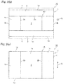
Fig.1 (a) is a front view showing astructure 1 of discharging heat of a light source device, according to the inventive example, andFig. 1(b) is a side view of thestructure 1. -
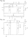
Fig. 2(a) is a front view showing astructure 10 obtained by forming electrodes on thestructure 1, andFig. 2(b) is a side view of thestructure 10. -
Fig. 3(a) is a front view showing alight source device 11 obtained by containing the light source device in thestructure 10, andFig. 3(b) is a side view of thelight source system 11. -
Fig. 4(a) is a plan view showing abase body 20 for film formation,Fig. 4(b) is a side view of thebase body 20, andFig. 4(c) shows state that aseed crystal film 21 formed on thebase body 20. -
Fig. 5(a) is a plan view showing abase body 20 and aseed crystal film 22 after patterning, andFig. 5(b) is a cross sectional view cut along Vb-Vb line ofFig. 5(a) . -
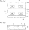
Fig. 6(a) is a plan view showing abase body 20 and afilm 23 of a nitride of a group 13 element, andFig. 6(b) is a cross sectional view cut along VIb-VIb line ofFig. 6(a) . -
Fig. 7(a) is a plan view showing a cross sectional face of thefilm 23 of a nitride of a group 13 element, andFig. 7(b) is a cross sectional view showing a cutting face of thefilm 23. - As shown in
Fig. 1 , astructure 1 of an inventive example is composes of a film of a nitride of a group 13 element.Fig. 1(a) is a diagram showing the film in a direction perpendicular to a direction A of thickness of the film, andFig. 1(b) is a diagram showing the film in the direction A of thickness of the film. - A through
hole 2 is provided in the film and is extended from a firstmain face 1c to a secondmain face 1d. According to the present example, thethrough hole 2 has a shape of a quadrilateral in a plan view. A pair ofinner wall faces 2a are thus opposed to each other across the throughhole 2. Further, a pair ofinner wall faces 2b are opposed to each other across the throughhole 2. According to the present example, a pair of theinner wall faces 2a is assigned to the fixing faces for fixing the light source device. As a result, thefixing faces 2a are utilized as the fixing faces for fixing the light source device and theinner wall faces 2b are formed on the sides ofmain wall portions 1b. - According to a preferred embodiment, an electrode for a light emitting device is provided in the inventive structure. For example, according to the
structure 10 shown inFig. 2 , a pair ofelectrodes 3 is provided on the firstmain face 1c of thestructure 1, andelectrodes 4 are further provided on an outerside end face 1e. Each of theelectrodes 4 is electrically connected to each of theelectrodes 3, and therespective electrodes 3 are separated from each other through the throughhole 2. A predetermined electric power can be supplied to the light source device through the pair of theelectrodes 3. -
Fig. 3 shows alight source system 11, in which alight source device 9 is contained in astructure 10. The throughhole 2 functions as aportion 15 of containing a light source device. The light source device is contained in the through hole, while the respective inner wall faces 2a function as the fixing faces of fixing the light source device. In this state, a pair of end faces 9a, 9b of thelight source device 9 contacts thefixing face 2a, andspaces 8 are formed between the inner wall faces 2b of the light source device andend faces 9c, respectively. In this state, wiring is provided between terminals (not shown) and theelectrodes 3 of the light source device so that the light source device is ready to operate. - According to the present invention, the heat discharge structure of the light source device is composed of a film of a nitride of a group 13 element. Group 13 element means group 13 element according to the Periodic Table determined by IUPAC. The group 13 element is specifically gallium, aluminum, indium, thallium or the like. The nitride of the group 13 element is most preferably GaN, AlN or AlGaN. Further, in the case that the contained optical device is a GaN-based optical device, the nitride of the group 13 element may most preferably be GaN. In the case that the film of the group 13 element is made of GaN, it becomes possible to reduce the difference of the thermal expansion coefficients of the contained GaN series optical device and the film of the nitride of the group 13 element. As a result, it is possible to prevent the damages of the optical device and the structure for discharging heat from the light source device, due to the difference of thermal expansion coefficients.
- The film of the nitride of the group 13 element includes the first main face, the second main face and the outer side end face. Here, although the planar shape of the film of the nitride of the group 13 element is not particularly limited, it may preferably be quadrilateral.
- It is provided, in the film of the nitride of the group 13 element, a portion of containing the light source device composed of a through hole opening at the first main face and second main face. Here, it is not necessary that the whole of the light source device is contained in the portion of containing the light source device, and a part of the
light source device 9 may be protruded from the throughhole 2, as shown inFig. 3(b) . - The face for fixing the light source device facing the through hole and contacting the light source is provided in the portion for containing the light source device. Then, upon emitting light, heat is conducted from the light source device to the heat discharge structure through the fixing face, and then finally discharged to the package.
- According to a preferred embodiment, a plurality of the faces for fixing the light source device are provided in the structure. It is thus possible to facilitate the discharge of the heat from the light source device. Preferably, two faces for fixing the light source device are provided in the structure. Most preferably, two faces for fixing the light source device are opposed to each other across the through hole.
- According to a preferred embodiment, a pair of electrodes for the light source device is provided on the first main face, and the electrodes are opposed to each other on the first main face across the through hole. When the inventive structure is produced, a lot of the structures are usually formed on a wafer at the same time. Thus, such electrodes on the main faces can be formed by patterning on the wafer, so that its productivity is particularly high.
- The difference of the thermal expansion coefficient of the base body of the light source device and the thermal expansion coefficient of the nitride of the group 13 element forming the inventive stricture may preferably be 20 percent or smaller of the thermal expansion coefficient of the nitride of the group 13 element forming the structure. On such viewpoint, the material forming the base body of the light source device may preferably be GaN, AlN or AlGaN.
- It will be described an example of producing the inventive structure below.
- First, as shown in
Figs. 4(a) and (b) , abase body 20 is prepared. Then, as shown inFig. 4(c) , aseed crystal film 21 is formed on a film-formingface 20a of thebase body 20. - A single crystal material, such as sapphire, GaN AlN, or the like, may be used for the base body. However, in applications providing a heat discharge structure as the present invention, it is more preferable to use an oriented ceramic material for the base body, on the viewpoint of reducing the cost. As such kind of the oriented ceramic material, aluminum oxide, zinc oxide and aluminum oxide are exemplified. More preferably, the base body is a substrate of aluminum oxide composed of a polycrystalline body whose c-axis is aligned substantially in a direction perpendicular to the main face.
- The method of forming the seed crystal film may preferably be vapor phase process, and metal organic chemical vapor deposition (MOCVD) method, hydride vapor phase epitaxy (HVPE) method, pulse-excited deposition (PXD) method, molecular beam epitaxy (MBE) method and sublimation method are exemplified. Metal organic chemical vapor deposition is most preferred.
- Then, as shown in
Fig. 5(a) and (b) , the seed crystal film is patterned by photo lithography to obtain patternedseed crystal films 22. Theseed crystal films 22 are provided on the base body (wafer) 20 in elongate strip-like shapes, respectively. As shown inFig. 5(a) , a space is provided between the adjacentseed crystal films 22, and asurface 20a of the base body is exposed to the space. Further, anopening 22a is formed at a predetermined position in each of theseed crystal films 22, and thesurface 20a of the base body is exposed through theopening 22a. - Then, as shown in
Fig. 6 , afilm 23 of a nitride of a group 13 element is formed on the seed crystal film. At this time, thefilm 23 of the nitride of the group 13 element is grown so as to conform to the planar shape of the underlyingseed crystal film 22. Here, according to a preferred embodiment, the seed crystal film and the film of the nitride of the group 13 element are formed of a same kind of material. In this case, as shown inFig. 6(b) , the seed crystal film and the film of the nitride of the group 13 element grown thereon are integrated with each other, so that the interface between them cannot be clearly distinguished. Thus, inFig. 6(b) , afilm 23 of a nitride of a group 13 element is shown on the base body and the seed crystal film is not separately depicted. - According to a preferred embodiment, the
film 23 of the nitride of the group 13 element is elongated horizontally in a shape of a stripe on the base body (wafer) 20. As shown inFig. 6(a) , a space is provided between theadjacent films 23 of the nitride of the group 13 element, and asurface 20a of the base body is exposed through the space. Further, anopening 23a is formed at a predetermined position in each of thefilms 23 of the nitride of the group 13 element, and thesurface 20a of the base body is exposed through theopening 23a. - The method of forming the film of the nitride of the group 13 element may be vapor phase process such as metal organic chemical vapor deposition (MOCVD) method, hydride vapor phase epitaxy (HVPE) method, pulse-excited deposition (PXD) method, MBE method and sublimation method or the like and liquid phase process such as flux method.
- According to a preferred embodiment, zinc is doped into the film of the nitride of the group 13 element. It is thus possible to improve the electrical insulation property of the film of the nitride of the group 13 element.
- After the film formation of the nitride of the group 13 element is finished, the underlying base body is removed. At this time, the seed crystal film may be left on the side of the thus formed nitride film of the group 13 element or may be removed with the base body. The removal of the base body may be performed by grinding or laser lift-off method. Then, one or both of the main faces of the film of the nitride of the group 13 element is polished when required.
- A lot of the structures are patterned at the same time on the film of the nitride of the group 13 element on the
base body 20. As a result, after the film of the nitride of the group 13 element is formed and the base body is removed, each of the films of the nitride of the group 13 element is cut along a cutting line D, for example, as shown inFig. 7 . It is thus possible to obtain the structure shown inFig. 1 .
Claims (10)
- A heat discharge structure for a light source device emitting a semiconductor laser, said structure fixing said light source device and discharging a heat, said structure comprising:a film of a nitride of a group 13 element, said film comprising a first main face, a second main face and an outer side end face;a portion for containing said light source device, said portion comprising a through hole opening at said first main face and said second main face, and;a fixing face for fixing said light source device, said fixing face facing said through hole and contacting said light source device.
- The structure of claim 1, comprising a plurality of said fixing faces for fixing said light source device.
- The structure of claim 2, wherein said fixing faces for fixing said light source device are opposed to each other across said through hole.
- The structure of any one of claims 1 to 3, wherein said nitride of said group 13 element comprises GaN.
- The structure of any one of claims 1 to 4, wherein said nitride of said group 13 element comprises zinc doped therein.
- The structure of any one of claims 1 to 5, further comprising an electrode for said light source device.
- The structure of claim 6, comprising a pair of said electrodes provided on said first main face and being opposed to each other across said through hole on said first main face.
- The structure of claim 6 or 7, further comprising an outer side electrode provided on said outer side end face.
- A light source system comprising said structure of any one of claims 1 to 8 and said light source device contained in said portion for containing said light source device and fixed on said fixing face.
- The system of claim 9, wherein said structure comprises a plurality of said fixing faces for fixing said light source device, and wherein said light source device contacts each of said fixing faces.
Applications Claiming Priority (1)
| Application Number | Priority Date | Filing Date | Title |
|---|---|---|---|
| JP2016012059A JP6510433B2 (en) | 2016-01-26 | 2016-01-26 | Method of manufacturing light source element heat dissipation structure |
Publications (2)
| Publication Number | Publication Date |
|---|---|
| EP3200251A1 true EP3200251A1 (en) | 2017-08-02 |
| EP3200251B1 EP3200251B1 (en) | 2019-12-04 |
Family
ID=57909462
Family Applications (1)
| Application Number | Title | Priority Date | Filing Date |
|---|---|---|---|
| EP17152832.6A Active EP3200251B1 (en) | 2016-01-26 | 2017-01-24 | Method of producing heat discharge structures for light source devices |
Country Status (3)
| Country | Link |
|---|---|
| US (2) | US20170211797A1 (en) |
| EP (1) | EP3200251B1 (en) |
| JP (1) | JP6510433B2 (en) |
Citations (3)
| Publication number | Priority date | Publication date | Assignee | Title |
|---|---|---|---|---|
| JPH01181490A (en) * | 1988-01-11 | 1989-07-19 | Canon Inc | Semiconductor laser device |
| US20140112363A1 (en) * | 2012-10-24 | 2014-04-24 | Alfred Feitisch | Solderless mounting for semiconductor lasers |
| US20150023376A1 (en) * | 2012-03-02 | 2015-01-22 | Panasonic Corporation | Semiconductor light-emitting device |
Family Cites Families (10)
| Publication number | Priority date | Publication date | Assignee | Title |
|---|---|---|---|---|
| US6355497B1 (en) * | 2000-01-18 | 2002-03-12 | Xerox Corporation | Removable large area, low defect density films for led and laser diode growth |
| JP2002057158A (en) | 2000-08-09 | 2002-02-22 | Sony Corp | Insulating nitride layer, method of forming the same, semiconductor device and method of manufacturing the same |
| JP4275336B2 (en) * | 2001-11-16 | 2009-06-10 | 株式会社半導体エネルギー研究所 | Method for manufacturing semiconductor device |
| JP2009064961A (en) * | 2007-09-06 | 2009-03-26 | Sharp Corp | Semiconductor laser device and manufacturing method thereof |
| US10125931B2 (en) * | 2008-03-01 | 2018-11-13 | Goldeneye, Inc. | Barrier with integrated self cooling solid state light sources |
| JP5216716B2 (en) * | 2008-08-20 | 2013-06-19 | 株式会社半導体エネルギー研究所 | Light emitting device and manufacturing method thereof |
| WO2010140370A1 (en) * | 2009-06-05 | 2010-12-09 | 住友化学株式会社 | Optical device, semiconductor substrate, optical device producing method, and semiconductor substrate producing method |
| US9583678B2 (en) * | 2009-09-18 | 2017-02-28 | Soraa, Inc. | High-performance LED fabrication |
| US9765934B2 (en) * | 2011-05-16 | 2017-09-19 | The Board Of Trustees Of The University Of Illinois | Thermally managed LED arrays assembled by printing |
| JP6133191B2 (en) * | 2013-10-18 | 2017-05-24 | 古河電気工業株式会社 | Nitride semiconductor device, diode, and field effect transistor |
-
2016
- 2016-01-26 JP JP2016012059A patent/JP6510433B2/en active Active
-
2017
- 2017-01-24 EP EP17152832.6A patent/EP3200251B1/en active Active
- 2017-01-24 US US15/413,992 patent/US20170211797A1/en not_active Abandoned
-
2018
- 2018-06-18 US US16/010,977 patent/US10598369B2/en not_active Expired - Fee Related
Patent Citations (3)
| Publication number | Priority date | Publication date | Assignee | Title |
|---|---|---|---|---|
| JPH01181490A (en) * | 1988-01-11 | 1989-07-19 | Canon Inc | Semiconductor laser device |
| US20150023376A1 (en) * | 2012-03-02 | 2015-01-22 | Panasonic Corporation | Semiconductor light-emitting device |
| US20140112363A1 (en) * | 2012-10-24 | 2014-04-24 | Alfred Feitisch | Solderless mounting for semiconductor lasers |
Non-Patent Citations (1)
| Title |
|---|
| KUZNETSOV N I ET AL: "Insulating GaN:Zn layers grown by hydride vapor phase epitaxy on SiC substrates", APPLIED PHYSICS LETTERS, A I P PUBLISHING LLC, US, vol. 75, no. 20, 15 November 1999 (1999-11-15), pages 3138 - 3140, XP012024048, ISSN: 0003-6951, DOI: 10.1063/1.125256 * |
Also Published As
| Publication number | Publication date |
|---|---|
| JP6510433B2 (en) | 2019-05-08 |
| EP3200251B1 (en) | 2019-12-04 |
| US20170211797A1 (en) | 2017-07-27 |
| US20180306428A1 (en) | 2018-10-25 |
| JP2017135178A (en) | 2017-08-03 |
| US10598369B2 (en) | 2020-03-24 |
Similar Documents
| Publication | Publication Date | Title |
|---|---|---|
| US11948980B1 (en) | Manufacturable thin film gallium and nitrogen containing devices | |
| US12464802B2 (en) | Manufacturable gallium and nitrogen containing single frequency laser diode | |
| US11011889B2 (en) | Manufacturable multi-emitter laser diode | |
| US9666677B1 (en) | Manufacturable thin film gallium and nitrogen containing devices | |
| CN204732408U (en) | Lighting device | |
| JP3348024B2 (en) | Semiconductor laser device | |
| JP5014967B2 (en) | Light emitting device and method for manufacturing light emitting device | |
| JP2007266577A (en) | Nitride semiconductor device and manufacturing method thereof | |
| US20080265272A1 (en) | Light Emitting Device Having Zener Diode Therein And Method Of Fabricating The Same | |
| CN101926012A (en) | Method for manufacturing light emitting device | |
| CN105406351B (en) | Laser diode device | |
| CN107026222B (en) | Light emitting element and method for manufacturing the same | |
| US10598369B2 (en) | Heat discharge structures for light source devices and light source systems | |
| JP2007116152A (en) | A-plane nitride semiconductor single crystal substrate having flat side surfaces | |
| US9299561B2 (en) | Method for fabricating nitride semiconductor thin film and method for fabricating nitride semiconductor device using the same | |
| JP2002111137A (en) | Semiconductor laser device | |
| US9159870B2 (en) | Method of fabricating gallium nitride based semiconductor device | |
| US11114817B2 (en) | Semiconductor laser device | |
| JP2002261370A (en) | Method for manufacturing nitride semiconductor device | |
| US20070085081A1 (en) | Thermally efficient semiconductor laser structure and method of forming same | |
| TW201601222A (en) | Method for separating release layer from substrate | |
| JP2000196145A (en) | Fabrication of semiconductor element |
Legal Events
| Date | Code | Title | Description |
|---|---|---|---|
| PUAI | Public reference made under article 153(3) epc to a published international application that has entered the european phase |
Free format text: ORIGINAL CODE: 0009012 |
|
| STAA | Information on the status of an ep patent application or granted ep patent |
Free format text: STATUS: THE APPLICATION HAS BEEN PUBLISHED |
|
| AK | Designated contracting states |
Kind code of ref document: A1 Designated state(s): AL AT BE BG CH CY CZ DE DK EE ES FI FR GB GR HR HU IE IS IT LI LT LU LV MC MK MT NL NO PL PT RO RS SE SI SK SM TR |
|
| AX | Request for extension of the european patent |
Extension state: BA ME |
|
| STAA | Information on the status of an ep patent application or granted ep patent |
Free format text: STATUS: REQUEST FOR EXAMINATION WAS MADE |
|
| 17P | Request for examination filed |
Effective date: 20180131 |
|
| RBV | Designated contracting states (corrected) |
Designated state(s): AL AT BE BG CH CY CZ DE DK EE ES FI FR GB GR HR HU IE IS IT LI LT LU LV MC MK MT NL NO PL PT RO RS SE SI SK SM TR |
|
| REG | Reference to a national code |
Ref country code: DE Ref legal event code: R079 Ref document number: 602017009204 Country of ref document: DE Free format text: PREVIOUS MAIN CLASS: H01L0033640000 Ipc: H01S0005022000 |
|
| GRAP | Despatch of communication of intention to grant a patent |
Free format text: ORIGINAL CODE: EPIDOSNIGR1 |
|
| STAA | Information on the status of an ep patent application or granted ep patent |
Free format text: STATUS: GRANT OF PATENT IS INTENDED |
|
| RIC1 | Information provided on ipc code assigned before grant |
Ipc: H01L 33/64 20100101ALI20190520BHEP Ipc: H01S 5/024 20060101ALI20190520BHEP Ipc: H01S 5/022 20060101AFI20190520BHEP Ipc: H01S 5/323 20060101ALN20190520BHEP |
|
| RIC1 | Information provided on ipc code assigned before grant |
Ipc: H01S 5/022 20060101AFI20190606BHEP Ipc: H01L 33/64 20100101ALI20190606BHEP Ipc: H01S 5/024 20060101ALI20190606BHEP Ipc: H01S 5/323 20060101ALN20190606BHEP |
|
| INTG | Intention to grant announced |
Effective date: 20190626 |
|
| GRAS | Grant fee paid |
Free format text: ORIGINAL CODE: EPIDOSNIGR3 |
|
| GRAA | (expected) grant |
Free format text: ORIGINAL CODE: 0009210 |
|
| STAA | Information on the status of an ep patent application or granted ep patent |
Free format text: STATUS: THE PATENT HAS BEEN GRANTED |
|
| AK | Designated contracting states |
Kind code of ref document: B1 Designated state(s): AL AT BE BG CH CY CZ DE DK EE ES FI FR GB GR HR HU IE IS IT LI LT LU LV MC MK MT NL NO PL PT RO RS SE SI SK SM TR |
|
| REG | Reference to a national code |
Ref country code: GB Ref legal event code: FG4D |
|
| REG | Reference to a national code |
Ref country code: CH Ref legal event code: EP |
|
| REG | Reference to a national code |
Ref country code: AT Ref legal event code: REF Ref document number: 1210600 Country of ref document: AT Kind code of ref document: T Effective date: 20191215 |
|
| REG | Reference to a national code |
Ref country code: DE Ref legal event code: R096 Ref document number: 602017009204 Country of ref document: DE |
|
| REG | Reference to a national code |
Ref country code: IE Ref legal event code: FG4D |
|
| REG | Reference to a national code |
Ref country code: NL Ref legal event code: MP Effective date: 20191204 |
|
| REG | Reference to a national code |
Ref country code: LT Ref legal event code: MG4D |
|
| PG25 | Lapsed in a contracting state [announced via postgrant information from national office to epo] |
Ref country code: BG Free format text: LAPSE BECAUSE OF FAILURE TO SUBMIT A TRANSLATION OF THE DESCRIPTION OR TO PAY THE FEE WITHIN THE PRESCRIBED TIME-LIMIT Effective date: 20200304 Ref country code: FI Free format text: LAPSE BECAUSE OF FAILURE TO SUBMIT A TRANSLATION OF THE DESCRIPTION OR TO PAY THE FEE WITHIN THE PRESCRIBED TIME-LIMIT Effective date: 20191204 Ref country code: LV Free format text: LAPSE BECAUSE OF FAILURE TO SUBMIT A TRANSLATION OF THE DESCRIPTION OR TO PAY THE FEE WITHIN THE PRESCRIBED TIME-LIMIT Effective date: 20191204 Ref country code: SE Free format text: LAPSE BECAUSE OF FAILURE TO SUBMIT A TRANSLATION OF THE DESCRIPTION OR TO PAY THE FEE WITHIN THE PRESCRIBED TIME-LIMIT Effective date: 20191204 Ref country code: NO Free format text: LAPSE BECAUSE OF FAILURE TO SUBMIT A TRANSLATION OF THE DESCRIPTION OR TO PAY THE FEE WITHIN THE PRESCRIBED TIME-LIMIT Effective date: 20200304 Ref country code: GR Free format text: LAPSE BECAUSE OF FAILURE TO SUBMIT A TRANSLATION OF THE DESCRIPTION OR TO PAY THE FEE WITHIN THE PRESCRIBED TIME-LIMIT Effective date: 20200305 Ref country code: LT Free format text: LAPSE BECAUSE OF FAILURE TO SUBMIT A TRANSLATION OF THE DESCRIPTION OR TO PAY THE FEE WITHIN THE PRESCRIBED TIME-LIMIT Effective date: 20191204 |
|
| PG25 | Lapsed in a contracting state [announced via postgrant information from national office to epo] |
Ref country code: HR Free format text: LAPSE BECAUSE OF FAILURE TO SUBMIT A TRANSLATION OF THE DESCRIPTION OR TO PAY THE FEE WITHIN THE PRESCRIBED TIME-LIMIT Effective date: 20191204 Ref country code: RS Free format text: LAPSE BECAUSE OF FAILURE TO SUBMIT A TRANSLATION OF THE DESCRIPTION OR TO PAY THE FEE WITHIN THE PRESCRIBED TIME-LIMIT Effective date: 20191204 |
|
| PG25 | Lapsed in a contracting state [announced via postgrant information from national office to epo] |
Ref country code: AL Free format text: LAPSE BECAUSE OF FAILURE TO SUBMIT A TRANSLATION OF THE DESCRIPTION OR TO PAY THE FEE WITHIN THE PRESCRIBED TIME-LIMIT Effective date: 20191204 |
|
| PG25 | Lapsed in a contracting state [announced via postgrant information from national office to epo] |
Ref country code: NL Free format text: LAPSE BECAUSE OF FAILURE TO SUBMIT A TRANSLATION OF THE DESCRIPTION OR TO PAY THE FEE WITHIN THE PRESCRIBED TIME-LIMIT Effective date: 20191204 Ref country code: CZ Free format text: LAPSE BECAUSE OF FAILURE TO SUBMIT A TRANSLATION OF THE DESCRIPTION OR TO PAY THE FEE WITHIN THE PRESCRIBED TIME-LIMIT Effective date: 20191204 Ref country code: ES Free format text: LAPSE BECAUSE OF FAILURE TO SUBMIT A TRANSLATION OF THE DESCRIPTION OR TO PAY THE FEE WITHIN THE PRESCRIBED TIME-LIMIT Effective date: 20191204 Ref country code: RO Free format text: LAPSE BECAUSE OF FAILURE TO SUBMIT A TRANSLATION OF THE DESCRIPTION OR TO PAY THE FEE WITHIN THE PRESCRIBED TIME-LIMIT Effective date: 20191204 Ref country code: EE Free format text: LAPSE BECAUSE OF FAILURE TO SUBMIT A TRANSLATION OF THE DESCRIPTION OR TO PAY THE FEE WITHIN THE PRESCRIBED TIME-LIMIT Effective date: 20191204 Ref country code: PT Free format text: LAPSE BECAUSE OF FAILURE TO SUBMIT A TRANSLATION OF THE DESCRIPTION OR TO PAY THE FEE WITHIN THE PRESCRIBED TIME-LIMIT Effective date: 20200429 |
|
| PG25 | Lapsed in a contracting state [announced via postgrant information from national office to epo] |
Ref country code: SM Free format text: LAPSE BECAUSE OF FAILURE TO SUBMIT A TRANSLATION OF THE DESCRIPTION OR TO PAY THE FEE WITHIN THE PRESCRIBED TIME-LIMIT Effective date: 20191204 Ref country code: SK Free format text: LAPSE BECAUSE OF FAILURE TO SUBMIT A TRANSLATION OF THE DESCRIPTION OR TO PAY THE FEE WITHIN THE PRESCRIBED TIME-LIMIT Effective date: 20191204 Ref country code: IS Free format text: LAPSE BECAUSE OF FAILURE TO SUBMIT A TRANSLATION OF THE DESCRIPTION OR TO PAY THE FEE WITHIN THE PRESCRIBED TIME-LIMIT Effective date: 20200404 |
|
| REG | Reference to a national code |
Ref country code: CH Ref legal event code: PL |
|
| REG | Reference to a national code |
Ref country code: DE Ref legal event code: R097 Ref document number: 602017009204 Country of ref document: DE |
|
| REG | Reference to a national code |
Ref country code: AT Ref legal event code: MK05 Ref document number: 1210600 Country of ref document: AT Kind code of ref document: T Effective date: 20191204 |
|
| PG25 | Lapsed in a contracting state [announced via postgrant information from national office to epo] |
Ref country code: MC Free format text: LAPSE BECAUSE OF FAILURE TO SUBMIT A TRANSLATION OF THE DESCRIPTION OR TO PAY THE FEE WITHIN THE PRESCRIBED TIME-LIMIT Effective date: 20191204 |
|
| PLBE | No opposition filed within time limit |
Free format text: ORIGINAL CODE: 0009261 |
|
| STAA | Information on the status of an ep patent application or granted ep patent |
Free format text: STATUS: NO OPPOSITION FILED WITHIN TIME LIMIT |
|
| REG | Reference to a national code |
Ref country code: BE Ref legal event code: MM Effective date: 20200131 |
|
| PG25 | Lapsed in a contracting state [announced via postgrant information from national office to epo] |
Ref country code: LU Free format text: LAPSE BECAUSE OF NON-PAYMENT OF DUE FEES Effective date: 20200124 Ref country code: DK Free format text: LAPSE BECAUSE OF FAILURE TO SUBMIT A TRANSLATION OF THE DESCRIPTION OR TO PAY THE FEE WITHIN THE PRESCRIBED TIME-LIMIT Effective date: 20191204 |
|
| 26N | No opposition filed |
Effective date: 20200907 |
|
| PG25 | Lapsed in a contracting state [announced via postgrant information from national office to epo] |
Ref country code: BE Free format text: LAPSE BECAUSE OF NON-PAYMENT OF DUE FEES Effective date: 20200131 Ref country code: SI Free format text: LAPSE BECAUSE OF FAILURE TO SUBMIT A TRANSLATION OF THE DESCRIPTION OR TO PAY THE FEE WITHIN THE PRESCRIBED TIME-LIMIT Effective date: 20191204 Ref country code: CH Free format text: LAPSE BECAUSE OF NON-PAYMENT OF DUE FEES Effective date: 20200131 Ref country code: LI Free format text: LAPSE BECAUSE OF NON-PAYMENT OF DUE FEES Effective date: 20200131 Ref country code: PL Free format text: LAPSE BECAUSE OF FAILURE TO SUBMIT A TRANSLATION OF THE DESCRIPTION OR TO PAY THE FEE WITHIN THE PRESCRIBED TIME-LIMIT Effective date: 20191204 Ref country code: AT Free format text: LAPSE BECAUSE OF FAILURE TO SUBMIT A TRANSLATION OF THE DESCRIPTION OR TO PAY THE FEE WITHIN THE PRESCRIBED TIME-LIMIT Effective date: 20191204 |
|
| PG25 | Lapsed in a contracting state [announced via postgrant information from national office to epo] |
Ref country code: IE Free format text: LAPSE BECAUSE OF NON-PAYMENT OF DUE FEES Effective date: 20200124 Ref country code: IT Free format text: LAPSE BECAUSE OF FAILURE TO SUBMIT A TRANSLATION OF THE DESCRIPTION OR TO PAY THE FEE WITHIN THE PRESCRIBED TIME-LIMIT Effective date: 20191204 |
|
| GBPC | Gb: european patent ceased through non-payment of renewal fee |
Effective date: 20210124 |
|
| PG25 | Lapsed in a contracting state [announced via postgrant information from national office to epo] |
Ref country code: GB Free format text: LAPSE BECAUSE OF NON-PAYMENT OF DUE FEES Effective date: 20210124 |
|
| PG25 | Lapsed in a contracting state [announced via postgrant information from national office to epo] |
Ref country code: TR Free format text: LAPSE BECAUSE OF FAILURE TO SUBMIT A TRANSLATION OF THE DESCRIPTION OR TO PAY THE FEE WITHIN THE PRESCRIBED TIME-LIMIT Effective date: 20191204 Ref country code: MT Free format text: LAPSE BECAUSE OF FAILURE TO SUBMIT A TRANSLATION OF THE DESCRIPTION OR TO PAY THE FEE WITHIN THE PRESCRIBED TIME-LIMIT Effective date: 20191204 Ref country code: CY Free format text: LAPSE BECAUSE OF FAILURE TO SUBMIT A TRANSLATION OF THE DESCRIPTION OR TO PAY THE FEE WITHIN THE PRESCRIBED TIME-LIMIT Effective date: 20191204 |
|
| PG25 | Lapsed in a contracting state [announced via postgrant information from national office to epo] |
Ref country code: MK Free format text: LAPSE BECAUSE OF FAILURE TO SUBMIT A TRANSLATION OF THE DESCRIPTION OR TO PAY THE FEE WITHIN THE PRESCRIBED TIME-LIMIT Effective date: 20191204 |
|
| PGFP | Annual fee paid to national office [announced via postgrant information from national office to epo] |
Ref country code: FR Payment date: 20221208 Year of fee payment: 7 |
|
| PGFP | Annual fee paid to national office [announced via postgrant information from national office to epo] |
Ref country code: DE Payment date: 20221130 Year of fee payment: 7 |
|
| REG | Reference to a national code |
Ref country code: DE Ref legal event code: R082 Ref document number: 602017009204 Country of ref document: DE Representative=s name: KRAUS & LEDERER PARTGMBB, DE |
|
| REG | Reference to a national code |
Ref country code: DE Ref legal event code: R119 Ref document number: 602017009204 Country of ref document: DE |
|
| PG25 | Lapsed in a contracting state [announced via postgrant information from national office to epo] |
Ref country code: DE Free format text: LAPSE BECAUSE OF NON-PAYMENT OF DUE FEES Effective date: 20240801 |
|
| PG25 | Lapsed in a contracting state [announced via postgrant information from national office to epo] |
Ref country code: FR Free format text: LAPSE BECAUSE OF NON-PAYMENT OF DUE FEES Effective date: 20240131 |
|
| PG25 | Lapsed in a contracting state [announced via postgrant information from national office to epo] |
Ref country code: FR Free format text: LAPSE BECAUSE OF NON-PAYMENT OF DUE FEES Effective date: 20240131 Ref country code: DE Free format text: LAPSE BECAUSE OF NON-PAYMENT OF DUE FEES Effective date: 20240801 |