EP3199988A1 - Color filter and manufacturing method thereof, display panel, display device and drive method thereof - Google Patents
Color filter and manufacturing method thereof, display panel, display device and drive method thereof Download PDFInfo
- Publication number
- EP3199988A1 EP3199988A1 EP15778592.4A EP15778592A EP3199988A1 EP 3199988 A1 EP3199988 A1 EP 3199988A1 EP 15778592 A EP15778592 A EP 15778592A EP 3199988 A1 EP3199988 A1 EP 3199988A1
- Authority
- EP
- European Patent Office
- Prior art keywords
- sub
- pixel
- pixels
- blue
- green
- Prior art date
- Legal status (The legal status is an assumption and is not a legal conclusion. Google has not performed a legal analysis and makes no representation as to the accuracy of the status listed.)
- Granted
Links
Images


Classifications
-
- G—PHYSICS
- G09—EDUCATION; CRYPTOGRAPHY; DISPLAY; ADVERTISING; SEALS
- G09G—ARRANGEMENTS OR CIRCUITS FOR CONTROL OF INDICATING DEVICES USING STATIC MEANS TO PRESENT VARIABLE INFORMATION
- G09G3/00—Control arrangements or circuits, of interest only in connection with visual indicators other than cathode-ray tubes
- G09G3/20—Control arrangements or circuits, of interest only in connection with visual indicators other than cathode-ray tubes for presentation of an assembly of a number of characters, e.g. a page, by composing the assembly by combination of individual elements arranged in a matrix no fixed position being assigned to or needed to be assigned to the individual characters or partial characters
- G09G3/2003—Display of colours
-
- G—PHYSICS
- G02—OPTICS
- G02B—OPTICAL ELEMENTS, SYSTEMS OR APPARATUS
- G02B30/00—Optical systems or apparatus for producing three-dimensional [3D] effects, e.g. stereoscopic images
- G02B30/20—Optical systems or apparatus for producing three-dimensional [3D] effects, e.g. stereoscopic images by providing first and second parallax images to an observer's left and right eyes
- G02B30/26—Optical systems or apparatus for producing three-dimensional [3D] effects, e.g. stereoscopic images by providing first and second parallax images to an observer's left and right eyes of the autostereoscopic type
- G02B30/27—Optical systems or apparatus for producing three-dimensional [3D] effects, e.g. stereoscopic images by providing first and second parallax images to an observer's left and right eyes of the autostereoscopic type involving lenticular arrays
-
- G—PHYSICS
- G02—OPTICS
- G02B—OPTICAL ELEMENTS, SYSTEMS OR APPARATUS
- G02B30/00—Optical systems or apparatus for producing three-dimensional [3D] effects, e.g. stereoscopic images
- G02B30/20—Optical systems or apparatus for producing three-dimensional [3D] effects, e.g. stereoscopic images by providing first and second parallax images to an observer's left and right eyes
- G02B30/26—Optical systems or apparatus for producing three-dimensional [3D] effects, e.g. stereoscopic images by providing first and second parallax images to an observer's left and right eyes of the autostereoscopic type
- G02B30/30—Optical systems or apparatus for producing three-dimensional [3D] effects, e.g. stereoscopic images by providing first and second parallax images to an observer's left and right eyes of the autostereoscopic type involving parallax barriers
-
- G—PHYSICS
- G02—OPTICS
- G02B—OPTICAL ELEMENTS, SYSTEMS OR APPARATUS
- G02B5/00—Optical elements other than lenses
- G02B5/20—Filters
- G02B5/201—Filters in the form of arrays
-
- G—PHYSICS
- G02—OPTICS
- G02B—OPTICAL ELEMENTS, SYSTEMS OR APPARATUS
- G02B5/00—Optical elements other than lenses
- G02B5/20—Filters
- G02B5/22—Absorbing filters
- G02B5/23—Photochromic filters
-
- G—PHYSICS
- G02—OPTICS
- G02F—OPTICAL DEVICES OR ARRANGEMENTS FOR THE CONTROL OF LIGHT BY MODIFICATION OF THE OPTICAL PROPERTIES OF THE MEDIA OF THE ELEMENTS INVOLVED THEREIN; NON-LINEAR OPTICS; FREQUENCY-CHANGING OF LIGHT; OPTICAL LOGIC ELEMENTS; OPTICAL ANALOGUE/DIGITAL CONVERTERS
- G02F1/00—Devices or arrangements for the control of the intensity, colour, phase, polarisation or direction of light arriving from an independent light source, e.g. switching, gating or modulating; Non-linear optics
- G02F1/01—Devices or arrangements for the control of the intensity, colour, phase, polarisation or direction of light arriving from an independent light source, e.g. switching, gating or modulating; Non-linear optics for the control of the intensity, phase, polarisation or colour
- G02F1/13—Devices or arrangements for the control of the intensity, colour, phase, polarisation or direction of light arriving from an independent light source, e.g. switching, gating or modulating; Non-linear optics for the control of the intensity, phase, polarisation or colour based on liquid crystals, e.g. single liquid crystal display cells
- G02F1/133—Constructional arrangements; Operation of liquid crystal cells; Circuit arrangements
- G02F1/1333—Constructional arrangements; Manufacturing methods
- G02F1/1335—Structural association of cells with optical devices, e.g. polarisers or reflectors
- G02F1/133509—Filters, e.g. light shielding masks
- G02F1/133512—Light shielding layers, e.g. black matrix
-
- G—PHYSICS
- G02—OPTICS
- G02F—OPTICAL DEVICES OR ARRANGEMENTS FOR THE CONTROL OF LIGHT BY MODIFICATION OF THE OPTICAL PROPERTIES OF THE MEDIA OF THE ELEMENTS INVOLVED THEREIN; NON-LINEAR OPTICS; FREQUENCY-CHANGING OF LIGHT; OPTICAL LOGIC ELEMENTS; OPTICAL ANALOGUE/DIGITAL CONVERTERS
- G02F1/00—Devices or arrangements for the control of the intensity, colour, phase, polarisation or direction of light arriving from an independent light source, e.g. switching, gating or modulating; Non-linear optics
- G02F1/01—Devices or arrangements for the control of the intensity, colour, phase, polarisation or direction of light arriving from an independent light source, e.g. switching, gating or modulating; Non-linear optics for the control of the intensity, phase, polarisation or colour
- G02F1/13—Devices or arrangements for the control of the intensity, colour, phase, polarisation or direction of light arriving from an independent light source, e.g. switching, gating or modulating; Non-linear optics for the control of the intensity, phase, polarisation or colour based on liquid crystals, e.g. single liquid crystal display cells
- G02F1/133—Constructional arrangements; Operation of liquid crystal cells; Circuit arrangements
- G02F1/1333—Constructional arrangements; Manufacturing methods
- G02F1/1335—Structural association of cells with optical devices, e.g. polarisers or reflectors
- G02F1/133509—Filters, e.g. light shielding masks
- G02F1/133514—Colour filters
-
- G—PHYSICS
- G02—OPTICS
- G02F—OPTICAL DEVICES OR ARRANGEMENTS FOR THE CONTROL OF LIGHT BY MODIFICATION OF THE OPTICAL PROPERTIES OF THE MEDIA OF THE ELEMENTS INVOLVED THEREIN; NON-LINEAR OPTICS; FREQUENCY-CHANGING OF LIGHT; OPTICAL LOGIC ELEMENTS; OPTICAL ANALOGUE/DIGITAL CONVERTERS
- G02F1/00—Devices or arrangements for the control of the intensity, colour, phase, polarisation or direction of light arriving from an independent light source, e.g. switching, gating or modulating; Non-linear optics
- G02F1/01—Devices or arrangements for the control of the intensity, colour, phase, polarisation or direction of light arriving from an independent light source, e.g. switching, gating or modulating; Non-linear optics for the control of the intensity, phase, polarisation or colour
- G02F1/13—Devices or arrangements for the control of the intensity, colour, phase, polarisation or direction of light arriving from an independent light source, e.g. switching, gating or modulating; Non-linear optics for the control of the intensity, phase, polarisation or colour based on liquid crystals, e.g. single liquid crystal display cells
- G02F1/133—Constructional arrangements; Operation of liquid crystal cells; Circuit arrangements
- G02F1/1333—Constructional arrangements; Manufacturing methods
- G02F1/1335—Structural association of cells with optical devices, e.g. polarisers or reflectors
- G02F1/133509—Filters, e.g. light shielding masks
- G02F1/133514—Colour filters
- G02F1/133516—Methods for their manufacture, e.g. printing, electro-deposition or photolithography
-
- G—PHYSICS
- G09—EDUCATION; CRYPTOGRAPHY; DISPLAY; ADVERTISING; SEALS
- G09G—ARRANGEMENTS OR CIRCUITS FOR CONTROL OF INDICATING DEVICES USING STATIC MEANS TO PRESENT VARIABLE INFORMATION
- G09G3/00—Control arrangements or circuits, of interest only in connection with visual indicators other than cathode-ray tubes
- G09G3/001—Control arrangements or circuits, of interest only in connection with visual indicators other than cathode-ray tubes using specific devices not provided for in groups G09G3/02 - G09G3/36, e.g. using an intermediate record carrier such as a film slide; Projection systems; Display of non-alphanumerical information, solely or in combination with alphanumerical information, e.g. digital display on projected diapositive as background
- G09G3/003—Control arrangements or circuits, of interest only in connection with visual indicators other than cathode-ray tubes using specific devices not provided for in groups G09G3/02 - G09G3/36, e.g. using an intermediate record carrier such as a film slide; Projection systems; Display of non-alphanumerical information, solely or in combination with alphanumerical information, e.g. digital display on projected diapositive as background to produce spatial visual effects
-
- G—PHYSICS
- G09—EDUCATION; CRYPTOGRAPHY; DISPLAY; ADVERTISING; SEALS
- G09G—ARRANGEMENTS OR CIRCUITS FOR CONTROL OF INDICATING DEVICES USING STATIC MEANS TO PRESENT VARIABLE INFORMATION
- G09G3/00—Control arrangements or circuits, of interest only in connection with visual indicators other than cathode-ray tubes
- G09G3/20—Control arrangements or circuits, of interest only in connection with visual indicators other than cathode-ray tubes for presentation of an assembly of a number of characters, e.g. a page, by composing the assembly by combination of individual elements arranged in a matrix no fixed position being assigned to or needed to be assigned to the individual characters or partial characters
- G09G3/2007—Display of intermediate tones
- G09G3/2074—Display of intermediate tones using sub-pixels
-
- G—PHYSICS
- G09—EDUCATION; CRYPTOGRAPHY; DISPLAY; ADVERTISING; SEALS
- G09G—ARRANGEMENTS OR CIRCUITS FOR CONTROL OF INDICATING DEVICES USING STATIC MEANS TO PRESENT VARIABLE INFORMATION
- G09G5/00—Control arrangements or circuits for visual indicators common to cathode-ray tube indicators and other visual indicators
- G09G5/14—Display of multiple viewports
-
- H—ELECTRICITY
- H04—ELECTRIC COMMUNICATION TECHNIQUE
- H04N—PICTORIAL COMMUNICATION, e.g. TELEVISION
- H04N13/00—Stereoscopic video systems; Multi-view video systems; Details thereof
- H04N13/30—Image reproducers
- H04N13/302—Image reproducers for viewing without the aid of special glasses, i.e. using autostereoscopic displays
- H04N13/31—Image reproducers for viewing without the aid of special glasses, i.e. using autostereoscopic displays using parallax barriers
-
- H—ELECTRICITY
- H04—ELECTRIC COMMUNICATION TECHNIQUE
- H04N—PICTORIAL COMMUNICATION, e.g. TELEVISION
- H04N13/00—Stereoscopic video systems; Multi-view video systems; Details thereof
- H04N13/30—Image reproducers
- H04N13/324—Colour aspects
-
- G—PHYSICS
- G09—EDUCATION; CRYPTOGRAPHY; DISPLAY; ADVERTISING; SEALS
- G09G—ARRANGEMENTS OR CIRCUITS FOR CONTROL OF INDICATING DEVICES USING STATIC MEANS TO PRESENT VARIABLE INFORMATION
- G09G2300/00—Aspects of the constitution of display devices
- G09G2300/04—Structural and physical details of display devices
- G09G2300/0439—Pixel structures
- G09G2300/0443—Pixel structures with several sub-pixels for the same colour in a pixel, not specifically used to display gradations
-
- G—PHYSICS
- G09—EDUCATION; CRYPTOGRAPHY; DISPLAY; ADVERTISING; SEALS
- G09G—ARRANGEMENTS OR CIRCUITS FOR CONTROL OF INDICATING DEVICES USING STATIC MEANS TO PRESENT VARIABLE INFORMATION
- G09G2300/00—Aspects of the constitution of display devices
- G09G2300/04—Structural and physical details of display devices
- G09G2300/0439—Pixel structures
- G09G2300/0452—Details of colour pixel setup, e.g. pixel composed of a red, a blue and two green components
Definitions
- At least one embodiment of the present disclosure further provides a display device, which comprises: the foregoing display panel, and a slit grating superimposed on the display panel.
- the size of the sub-sub-pixels included by one sub-pixel in the embodiment of the present disclosure is the same with the size of one sub-pixel in FIG. 5 , the size of a single sub-pixel in the embodiment of the present disclosure is larger, so that the requirement on the fineness of a mask for forming the sub-pixels can be reduced and the alignment of the mask can be easier, and hence the manufacturing difficulty of the color filter can be reduced.
Landscapes
- Physics & Mathematics (AREA)
- General Physics & Mathematics (AREA)
- Engineering & Computer Science (AREA)
- Optics & Photonics (AREA)
- Nonlinear Science (AREA)
- Computer Hardware Design (AREA)
- Theoretical Computer Science (AREA)
- Multimedia (AREA)
- Signal Processing (AREA)
- Mathematical Physics (AREA)
- Chemical & Material Sciences (AREA)
- Crystallography & Structural Chemistry (AREA)
- Manufacturing & Machinery (AREA)
- Liquid Crystal (AREA)
Abstract
Description
- At least one embodiment of the present disclosure relates to a color filter and a manufacturing method thereof, a display panel, a display device and a driving method thereof.
- A grating 3D (namely, three-dimensional) display device mainly comprises: a display screen and a grating superimposed on the front or back of the display screen. The display screen includes a plurality of sub-pixels arranged in a matrix. The grating includes light-blocking strips and light-transmitting strips, which are alternately arranged. Upon 3D display being performed, a left-eye image signal is applied to half of the sub-pixels of the display screen and a right-eye image signal is applied to the other half of the sub-pixels; and the sub-pixels applied with the left-eye image signal and the sub-pixels applied with the right-eye image signal are alternately arranged along a row direction.
- When a person views a display image at an appropriate position, because there is a certain distance between a left eye and a right eye, namely the viewing angle of the left eye and the viewing angle of the right eye are different, and the light-blocking strips of the grating have a certain blocking function on the sub-pixels, the left eye can only receive light passing through the sub-pixels applied with the left-eye image signal and the right eye can only receive light passing through the sub-pixels applied with the right-eye image signal, and hence the left-eye image light and the right-eye image light are separated in space. Because a left-eye image and a right-eye image are images captured from different angles, the left-eye image and the right-eye image are superimposed in the brain, and hence the 3D display effect can be produced.
- At least one embodiment of the present disclosure provides a color filter and a manufacturing method thereof, a display panel, and a display device and a driving method thereof, so as to reduce the manufacturing difficulty of the color filter on the premise of not reducing the resolution.
- At least one embodiment of the present disclosure provides a color filter, which comprises a black matrix, a plurality of color resists and a plurality of pixel regions arranged in a matrix. The black matrix includes a plurality of first black matrix strips extending along a row direction and a plurality of second black matrix strips extending along a column direction, and the plurality of first black matrix strips and the plurality of second black matrix strips are intersected with each other to form a plurality of mesh regions arranged in a matrix; the plurality of color resists is respectively disposed in the plurality of mesh regions and includes red resists, green resists and blue resists; each pixel region includes a red sub-pixel region, a green sub-pixel region and a blue sub-pixel region; the red sub-pixel region includes an even number of red sub-sub-pixel regions, each red sub-sub-pixel region is provided with one of the red resists therein; the green sub-pixel region includes an even number of green sub-sub-pixel regions, each green sub-sub-pixel region is provided with one of the green resists therein; and the blue sub-pixel region includes an even number of blue sub-sub-pixel regions, and each blue sub-sub-pixel region is provided with one of the blue resists therein.
- At least one embodiment of the present disclosure further provides a color filter manufacturing method for manufacturing the foregoing color filter. The manufacturing method comprises: forming a black matrix on a substrate, so that the black matrix includes a plurality of first black matrix strips extending along a row direction and a plurality of second black matrix strips extending along a column direction, and the plurality of first black matrix strips and the plurality of second black matrix strips are intersected with each other to form a plurality of mesh regions arranged in a matrix; and forming a plurality of color resists respectively in the plurality of mesh regions formed by the black matrix, so that the plurality of color resists comprises red resists, green resists and blue resists; the color filter includes a plurality of pixel regions arranged in a matrix; each pixel region includes a red sub-pixel region, a green sub-pixel region and a blue sub-pixel region; the red sub-pixel region includes an even number of red sub-sub-pixel regions, each red sub-sub-pixel region is provided with one of the red resists therein, the green sub-pixel region includes an even number of green sub-sub-pixel regions, each green sub-sub-pixel region is provided with one of the green resists therein, the blue sub-pixel region includes an even number of blue sub-sub-pixel regions, and each blue sub-sub-pixel region is provided with one of the blue resists therein.
- At least one embodiment of the present disclosure further provides a display panel, which comprises: the foregoing color filter.
- At least one embodiment of the present disclosure further provides a display device, which comprises: the foregoing display panel, and a slit grating superimposed on the display panel.
- At least one embodiment of the present disclosure further provides a driving method for the display device. The display panel of the display device includes a plurality of pixels arranged in a matrix; each pixel includes a red sub-pixel, a green sub-pixel and a blue sub-pixel; the red sub-pixel includes an even number of red sub-sub-pixels, the green sub-pixel includes an even number of green sub-sub-pixels, and the blue sub-pixel includes an even number of blue sub-sub-pixels. The driving method comprises: within a time period of one frame, applying a left-eye image signal to half of red sub-sub-pixels of each red sub-pixel, half of green sub-sub-pixels of each green sub-pixel, and half of blue sub-sub-pixels of each blue sub-pixel, and meanwhile applying a right-eye image signal to the other half of red sub-sub-pixels of each red sub-pixel, the other half of green sub-sub-pixels of each green sub-pixel, and the other half of blue sub-sub-pixels of each blue sub-pixel; and meanwhile driving the slit grating to form light-blocking strips and light-transmitting strips, which are alternated, so that upon the display device being viewed at a predetermined viewing position, light passing through the sub-sub-pixels applied with the right-eye image signal is blocked by the light-blocking strips and cannot enter a left eye and light passing through the sub-sub-pixels applied with the left-eye image signal is transmitted from the light-transmitting strips and enters the left eye, the light passing through the sub-sub-pixels applied with the left-eye image signal is blocked by the light-blocking strips and cannot enter a right eye and the light passing through the sub-sub-pixels applied with the right-eye image signal is transmitted from the light-transmitting strips and enters the right eye.
- In order to clearly illustrate the technical solution of the embodiments of the disclosure, the drawings of the embodiments will be briefly described in the following; it is obvious that the described drawings are only related to some embodiments of the disclosure and thus are not limitative of the disclosure.
-
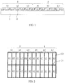
FIG. 1 is a sectional view of a color filter provided by an embodiment of the present disclosure; -
FIG. 2 is a plan view of a color filter provided by an embodiment of the present disclosure; -
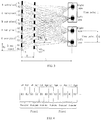
FIG. 3 is a view of a light path in the case of 3D display performed by a display device provided by an embodiment of the present disclosure; -
FIG. 4 is a drive schematic view of a display device provided by an embodiment of the present disclosure; -
FIG. 5 is a drive schematic view of a 3D display device; -
FIGS. 6 to 9 are views illustrating steps of a color filter manufacturing method provided by an embodiment of the present disclosure; and -
FIG. 10 is a schematic structural sectional view of a display panel provided by an embodiment of the present disclosure. - In order to make objects, technical details and advantages of the embodiments of the disclosure apparent, the technical solutions of the embodiments will be described in a clearly and fully understandable way in connection with the drawings related to the embodiments of the disclosure. Apparently, the described embodiments are just a part but not all of the embodiments of the disclosure. Based on the described embodiments herein, those skilled in the art can obtain other embodiment(s), without any inventive work, which should be within the scope of the disclosure.
- In the study, the inventors of the present application noticed that: the color of the sub-pixels of a display screen is generally arranged according to the circulation of the sequence of red (R), green (G) and blue (B); a pixel is formed by one red sub-pixel, one green sub-pixel and one blue sub-pixel; and each sub-pixel includes a color resist disposed on a color filter correspondingly. For the pursuit of high resolution, the size of the sub-pixels is smaller and smaller and the requirements on the manufacturing precision and the alignment accuracy of masks for forming the color resists is higher and higher, and this causes the increase of difficulty in manufacturing the color filter.
- At least one embodiment of the present disclosure provides a color filter. As illustrated in
FIGS. 1 and 2 , the color filter comprises asubstrate 1, ablack matrix 2 disposed on thesubstrate 1, and a plurality of color resists. Theblack matrix 2 includes a plurality of firstblack matrix strips 21 extending along a row direction and a plurality of secondblack matrix strips 22 extending along a column direction; the plurality of firstblack matrix strips 21 and the plurality of secondblack matrix strips 22 are intersected with each other to form a plurality of mesh regions arranged in a matrix; and the plurality of color resists is respectively disposed in the plurality of mesh regions and comprises red (R) resists, green (G) resists and blue (B) resists. - The arrangement of the color resists on the above-mentioned color filter is as follows: a plurality of pixel regions A arranged in a matrix is included; each pixel region A includes an R sub-pixel region A1, a G sub-pixel region A2 and a B sub-pixel region A3; the R sub-pixel region A1 includes an even number of R sub-sub-pixel regions, each R sub-sub-pixel region is provided with an R resist (referring to R1 or R2 in
FIGS. 1 and 2 ); the G sub-pixel region A2 includes an even number of G sub-sub-pixel regions, each G sub-sub-pixel region is provided with a G resist (referring to G1 or G2 inFIGS. 1 and 2 ); and the B sub-pixel region A3 includes an even number of B sub-sub-pixel regions, and each B sub-sub-pixel region is provided with a B resist (referring to B1 or B2 inFIGS. 1 and 2 ). - In an embodiment of the present disclosure, the
substrate 1, for instance, can be a glass substrate, a quartz substrate, or a plastic substrate, etc. Theblack matrix 2, for instance, can adopt a black light-blocking resin material. No limitations are imposed in the embodiment of the present disclosure. - Correspondingly, at least one embodiment of the present disclosure provides a method for manufacturing the foregoing color filter. The method comprises the following step S1 and step S2.
- Step S1: forming a
black matrix 2 on asubstrate 1, so that theblack matrix 2 includes a plurality of firstblack matrix strips 21 extending along a row direction and a plurality of secondblack matrix strips 22 extending along a column direction, and the plurality of firstblack matrix strips 21 and the plurality of secondblack matrix strips 22 are intersected with each other to form a plurality of mesh regions arranged in a matrix. - Step S2: forming a plurality of color resists respectively in the plurality of mesh regions formed by the
black matrix 2, so that the plurality of color resists comprises red resists, green resists and blue resists. The arrangement of the color resists on this color filter can refer to the above description relating to the arrangement of the color resists on the color filter, and repeated descriptions are omitted thereto. - Correspondingly, at least one embodiment of the present disclosure further provides a display panel, which comprises the foregoing color filter. The display panel can be a liquid crystal display (LCD) panel, or an organic light-emitting diode (OLED) panel, etc. No limitations is imposed in the embodiment of the present disclosure.
- In at least one embodiment, the display panel can comprise an
array substrate 20 and a cell-assembledsubstrate 30 arranged to be opposite to thearray substrate 20, as shown inFIG. 10 . For instance, thearray substrate 20 and the cell-assembledsubstrate 30 can be sealed by aframe sealant 40 to form a liquid crystal cell, and a liquid crystal material is filled in the liquid crystal cell. - In at least one embodiment, the color filter can be arranged to be opposite to the array substrate; or the color filter can be disposed in the array substrate. For instance,
FIG. 10 is a schematic structural view of a display panel in which a color filter and an array substrate are arranged to be opposite to each other. As illustrated inFIG. 10 , the display panel can comprise anarray substrate 20 and a cell-assembledsubstrate 30 arranged to be opposite to each other; the color filter is disposed in the cell-assembledsubstrate 30, the above-mentionedsubstrate 1 included by the color filter can be taken as a base substrate of the cell-assembledsubstrate 30, and theblack matrix 2 is disposed on thesubstrate 1 and faces thearray substrate 20. For instance, in a situation in which the color filter is disposed in the array substrate, the cell-assembled substrate, arranged to be opposite to the array substrate, in the display panel can be a transparent substrate. No limitations are imposed in the embodiment of the present disclosure. - Correspondingly, at least one embodiment of the present disclosure further provides a 3D display device. As illustrated in
FIG. 3 , the 3D display device comprises the foregoing display panel 3 and a slit grating 4 superimposed on the display panel 3. In the embodiment of the present disclosure, the slit grating 4 is disposed on a light-emitting surface of the display panel 3. The display panel 3 includes a plurality of pixels arranged in a matrix, each pixel includes an R sub-pixel, a G sub-pixel and a B sub-pixel; and the R sub-pixel includes an even number of R sub-sub-pixels, the G sub-pixel includes an even number of G sub-sub-pixels, and the B sub-pixel includes an even number of B sub-sub-pixels. - It should be noted that: in order to highlight the blocking and transmitting function of the slit grating 4 on pixels in the display surface of the display panel 3, the display panel 3 shown in
FIG. 3 is simplified as the arrangement of the pixels in the display surface, and there is a certain distance D between the slit grating 4 and the display surface of the display panel 3. Actually, the slit grating 4 and the display panel 3 are attached together, and the distance D between the slit grating 4 and the display surface of the display panel 3 depends on the thickness of a substrate, of the display panel 3, on a side close to the slit grating 4. - Correspondingly, at least one embodiment of the present disclosure further provides a driving method for the above-mentioned display device. As illustrated in
FIGS. 3 and 4 , the driving method comprises: within a time period of one frame, applying a left-eye image signal to half of R sub-sub-pixels of each R sub-pixel, half of G sub-sub-pixels of each G sub-pixel and half of B sub-sub-pixels of each B sub-pixel, and meanwhile applying a right-eye image signal to the other half of R sub-sub-pixels of each R sub-pixel, the other half of G sub-sub-pixels of each G sub-pixel and the other half of B sub-sub-pixels of each B sub-pixel; and meanwhile driving the slit grating 4 to form light-blocking strips 41 and light-transmittingstrips 42, which are alternated, so that upon the display device being viewed at a predetermined viewing position, light passing through the sub-sub-pixels applied with the right-eye image signal is blocked by the light-blocking strips 41 and cannot enter the left eye, light passing through the sub-sub-pixels applied with the left-eye image signal is transmitted from the light-transmittingstrips 42 and enters the left eye, the light passing through the sub-sub-pixels applied with the left-eye image signal is blocked by the light-blocking strips 41 and cannot enter the right eye, and the light passing through the sub-sub-pixels applied with the right-eye image signal is transmitted from the light-transmittingstrips 42 and enters the right eye. - By utilization of the pixel arrangement structure and the driving method, in a situation in which a person views the display device at a certain position, because there is parallax between the left eye and the right eye, the light entering the left eye is only the light passing through the sub-sub-pixels applied with the left-eye image signal and the light entering the right eye is only the light passing through the sub-sub-pixels applied with the right-eye image signal, the left-eye image and the right-eye image are superimposed and synthesized in the human brain, and hence the 3D image effect can be produced.
- As illustrated in
FIG. 5 , the arrangement of a color filter of a 3D display device is provided according to circulation of the sequence of R sub-pixels, B sub-pixels and G sub-pixels. In the case of 3D display, in two adjacent sub-pixels, one is applied with a left-eye image signal and the other is applied with a right-eye image signal, and hence the 3D display can be achieved. The arrangement of the color filter in an embodiment of the present disclosure is also provided according to the circulation of the sequence of R sub-pixels, B sub-pixels and G sub-pixels, and has difference that: each sub-pixel is also subdivided into an even number of sub-sub-pixels with the same color; the size of each sub-sub-pixel can be the same with the size of one sub-pixel inFIG. 5 ; the even number of the sub-sub-pixels of each sub-pixel are uniformly divided into two parts, one part of which is applied with a left-eye image signal and the other part of which is applied with a right-eye image signal; and hence the 3D display function can be achieved. - On the basis of achieving 3D display, the size of each sub-sub-pixel in the embodiment of the present disclosure can be set to be the same with the size of one sub-pixel in
FIG. 5 , so that the resolution of the 3D display device in the embodiment of the present disclosure is the same with the resolution of the 3D display device shown inFIG. 5 . Meanwhile, because the sub-sub-pixels included by each sub-pixel in the embodiment of the present disclosure have the same color and are adjacent to each other in position, all the sub-sub-pixels included by one sub-pixel can be formed in a same step, namely the sub-pixels of one color can be formed in one step. Moreover, because the size of the sub-sub-pixels included by one sub-pixel in the embodiment of the present disclosure is the same with the size of one sub-pixel inFIG. 5 , the size of a single sub-pixel in the embodiment of the present disclosure is larger, so that the requirement on the fineness of a mask for forming the sub-pixels can be reduced and the alignment of the mask can be easier, and hence the manufacturing difficulty of the color filter can be reduced. - In the color filter provided by the embodiment of the present disclosure, the number of the red sub-sub-pixel regions included by the red sub-pixel region A1 (namely the number of the arranged R resists), the number of the green sub-sub-pixel regions included by the green sub-pixel region A2 (namely the number of the arranged G resists), and the number of the blue sub-sub-pixel regions included by the blue sub-pixel region A3 (namely the number of the arranged B resists) can be set to be identical.
- On the premise of not obviously influencing the display quality, in at least one embodiment of the present disclosure, each sub-pixel region of the color filter includes two sub-sub-pixel regions with the same color (namely two color resists with a same color are arranged). For instance, the R sub-pixel region A1 includes two R sub-sub-pixel regions (namely two R resists R1 and R2 are arranged); the G sub-pixel region A2 includes two G sub-sub-pixel regions (namely two G resists G1 and G2 are arranged); and the B sub-pixel region A3 includes two B sub-sub-pixel regions (namely two B resists B1 and B2 are arranged). Of course, the embodiment of the present disclosure is not limited thereto.
- At this point, in the case of driving the display device, a left-eye image signal is applied to one sub-sub-pixel in each sub-pixel and a right-eye image signal is applied to the other sub-sub-pixel; and in one row of sub-sub-pixels, the sub-sub-pixels applied with the left-eye image signal and the sub-sub-pixels applied with the right-eye image signal are alternately arranged. That is to say, the sub-sub-pixels applied with the left-eye image signal are R1, G1 and B1, and the sub-sub-pixels applied with the right-eye image signal are R2, G2 and B2.
- To put it another way, because odd columns of sub-pixels are formed by R1, G1 and B1 and even columns of sub-pixels are formed by R2, G2 and B2, in the case of driving, within the time period of one frame, a left-eye image signal is applied to the odd columns of sub-sub-pixels R1, G1 and B1 and meanwhile a right-eye image signal is applied to the even columns of sub-sub-pixels R2, G2 and B2. Meanwhile, a slit grating 4 is driven to form light-blocking strips 41 and light-transmitting
strips 42, which are alternated, so that upon the display device being viewed at a predetermined viewing position, light passing through the even columns of sub-sub-pixels R2, G2 and B2 is blocked by the light-blocking strips 41 and cannot enter the left eye, light passing through the odd columns of sub-sub-pixels R1, G1 and B1 is transmitted from the light-transmittingstrips 42 and enters the left eye, namely the left eye can only view the odd columns of sub-sub-pixels R1, G1 and B1; and so that the light passing through the odd columns of sub-sub-pixels R1, G1 and B1 is blocked by the light-blocking strips 41 and cannot enter the right eye, and the light passing through the even columns of sub-sub-pixels R2, G2 and B2 is transmitted from the light-transmittingstrips 42 and enters the right eye, namely the right eye can only view the even columns of sub-sub-pixels R2, G2 and B2; and hence the left-eye image light and the right-eye image light are separated in space. - Of course, a right-eye image signal can also be applied to odd columns of sub-sub-pixels R1, G1 and B1 and meanwhile a left-eye image signal can be applied to even columns of sub-sub-pixels R2, G2 and B2. Meanwhile, a slit grating 4 is driven to form light-blocking strips 41 and light-transmitting
strips 42, which are alternated, so that upon the display device being viewed at a predetermined viewing position, light passing through the odd columns of sub-sub-pixels R1, G1 and B1 is blocked by the light-blocking strips 41 and cannot enter the left eye and light passing through the even columns of sub-sub-pixels R2, G2 and B2 is transmitted from the light-transmittingstrips 42 and enters the left eye, namely the left eye can only view the even columns of sub-sub-pixels R2, G2 and B2; the light passing through the even columns of sub-sub-pixels R2, G2 and B2 is blocked by the light-blocking strips 41 and cannot enter the right eye and the light passing through the odd columns of sub-sub-pixels R1, G1 and B1 is transmitted from the light-transmittingstrips 42 and enters the right eye, namely the right eye can only view the odd columns of sub-sub-pixels R1, G1 and B1; and hence the left-eye image light and the right-eye image light are separated in space. - Taking the case that each sub-pixel includes two sub-sub-pixels with a same color, namely each sub-pixel region of the color filter is provided with two color resists with a same color, as an example, the manufacturing process of the color filter, for instance, can include the following steps S01 to S04. The steps will be described below one by one.
- Step S01: as illustrated in
FIG. 6 , forming a pattern comprising ablack matrix 2 on asubstrate 1. - Step S02: as illustrated in
FIG. 7 , forming R resists R1 and R2 in R sub-pixel regions A1 by a patterning process. - For instance, an R resist material is spin-coated on the substrate; subsequently, the R resist material is subjected to exposure by using a mask, of which the sub-pixel width is twice the sub-pixel width of the color filter in
FIG. 5 , and to development; partial R resist material is removed and the R resist material.in the R sub-pixel regions A1 to be formed is retained; and the R resists R1 and R2 are formed. The formed R resists R1 and R2 are disposed in two adjacent mesh regions formed by theblack matrix 2. - Step S03: as illustrated in
FIG. 8 , forming G resists G1 and G2 in G sub-pixel regions A2 by a patterning process. - For instance, a G resist material is spin-coated on the substrate; subsequently, the G resist material is subjected to exposure by using a mask, of which the sub-pixel width is twice the sub-pixel width of the color filter in
FIG. 5 , and to development; partial G resist material is removed and the G resist material in the G sub-pixel regions A2 to be formed is retained; and the G resists G1 and G2 are formed. The formed G resists G1 and G2 are disposed in two adjacent mesh regions formed by theblack matrix 2. - Step S04: as illustrated in
FIG. 9 , forming B resists B1 and B2 in B sub-pixel regions A3 by a patterning process. - For instance, a B resist material is spin-coated on the substrate; subsequently, the B resist material is subjected to exposure by using a mask, of which the sub-pixel width is twice the sub-pixel width of the color filter in
FIG. 5 , and to development; partial B resist material is removed and the B resist material in the B sub-pixel regions A3 to be formed is retained; and the B resists B1 and B2 are formed. The formed B resists B1 and B2 are disposed in two adjacent mesh regions formed by theblack matrix 2. - It should be noted that the forming sequence of the R sub-pixels, the G sub-pixels and the B sub-pixels is not limited in the embodiment of the present disclosure.
- In addition, the method adopted by the above-mentioned manufacturing process relates to a pigment dispersion method. On the basis of the structure of the color filter provided by the embodiment of the present disclosure, the methods such as printing method, slurry jet method and organic material plating method can also be adopted by those skilled in the art for manufacturing the color filter.
- It should be noted that
FIG. 4 only illustrates the arrangement condition of one row of sub-sub-pixels in the display device. Actually, the display device includes a plurality of rows of sub-sub-pixels arranged in accordance withFIG. 4 . - In the embodiment of the present disclosure, it is supposed that the width Ww of a slit of the grating 4, the width Ws of a grating unit (namely the sum of the width of one light-blocking strip and the width of one light-transmitting strip), and the distance D between the grating 4 and the display surface of the display panel 3 can be obtained by the calculation of the width Wp of a single sub-pixel in the display panel 3 (namely the sum of the widths of the even number of sub-sub-pixels belonging to the same sub-pixel; illustration is given in
FIG. 3 by taking two sub-sub-pixels as an example), the distance Q between the left eye and the right eye of a human being, and the distance L between the display surface of the display panel 3 and the human eyes (namely the foregoing "viewing position"). - In general, it can be considered that the distance Q between the left eye and the right eye of the human being and the distance L between the display surface of the display panel 3 and the human eyes are unchanged and Ww, Ws and D are determined by the width Wp of the pixel. The value of Wp refers to the sum of the widths of the sub-sub-pixels included by a single sub-pixel. The width of a single sub-sub-pixel is the same with the width of a single sub-pixel in
FIG. 5 . After the value Wp is respectively substituted into the formulas:


- The display panel 3 (comprising the color filter) and the grating 4 are set according to the calculated size. When a human views images at view points (e.g., a
view point 1 and a view point 2) in front of the display device, due to the blocking function of the light-blocking strips 41 of the grating 4, the sub-sub-pixels that the left eye views are only the sub-sub-pixels R1, G1 and B1 through the light-transmittingstrips 42 of the grating 4 and the sub-sub-pixels that the right eye views are only the sub-sub-pixels R2, G2 and B2 through the light-transmittingstrips 42 of the grating 4. The sub-sub-pixels R1, G1 and B1 are driven to display the left-eye image (or the right-eye image), the sub-sub-pixels R2, G2 and B2 are driven to display the right-eye image (or the left-eye image), and because the left-eye image and the right-eye image are images captured from different angles, a 3D image can be obtained by the superimposition of the left-eye image and the right-eye image received by the two eyes of the human being. - It should be noted that the display device provided by the embodiment of the present disclosure can be a liquid crystal display panel, an e-paper, an OLED (organic Light-Emitting Diode) panel or the like and is applicable to any product or component with display function such as a mobile phone, a tablet PC, a TV, a display, a notebook computer, a digital picture frame and a navigator.
- In the color filter and the manufacturing method thereof, the display panel, and the display device and the driving method thereof, provided by the embodiments of the present disclosure, an even number of color resists with a same color are disposed in each sub-pixel region of the color filter; each color resist corresponds to a sub-sub-pixel region; a left-eye image signal is applied to half of sub-sub-pixels of each sub-pixel and meanwhile a right-eye image signal is applied to the other half of the sub-sub-pixels; and hence 3D display can be achieved. Obviously, the size of the sub-sub-pixels in the embodiments of the present disclosure can be the same with the size of the sub-pixels in the color filter as shown in
FIG. 5 . That is to say, the resolution of the color filter in the embodiments of the present disclosure is the same with the resolution of the color filter inFIG. 5 , and the size of the sub-pixel can be set to be at least twice as large as the size of the sub-pixel of the color filter inFIG. 5 . Moreover, all the sub-sub-pixels in the sub-pixels of one color have a same color and can be formed in a same step. Therefore, the manufacturing precision and the alignment accuracy of a mask required for manufacturing the color filter provided by the embodiments of the present disclosure can be reduced, and hence the manufacturing difficulty of the color filter can be reduced. - What are described above is related to the illustrative embodiments of the disclosure only and not limitative to the scope of the disclosure; the scopes of the disclosure are defined by the accompanying claims.
- The application claims priority to the
Chinese Patent Application No. 201410509950.7, filed on September 28, 2014
Claims (11)
- A color filter, comprising:a black matrix, wherein the black matrix comprises a plurality of first black matrix strips extending along a row direction and a plurality of second black matrix strips extending along a column direction, and the plurality of first black matrix strips and the plurality of second black matrix strips are intersected with each other to form a plurality of mesh regions arranged in a matrix;a plurality of color resists respectively disposed in the plurality of mesh regions and comprising red resists, green resists and blue resists; anda plurality of pixel regions arranged in a matrix, wherein each of the pixel regions comprises a red sub-pixel region, a green sub-pixel region and a blue sub-pixel region; the red sub-pixel region comprises an even number of red sub-sub-pixel regions, each of the red sub-sub-pixel regions is provided with one of the red resists therein; the green sub-pixel region comprises an even number of green sub-sub-pixel regions, each of the green sub-sub-pixel regions is provided with one of the green resists therein; and the blue sub-pixel region comprises an even number of blue sub-sub-pixel regions, and each of the blue sub-sub-pixel regions is provided with one of the blue resists therein.
- The color filter according to claim 1, wherein the number of the red sub-sub-pixel regions in the red sub-pixel region, the number of the green sub-sub-pixel regions in the green sub-pixel region, and the number of the blue sub-sub-pixel regions in the blue sub-pixel region are identical.
- The color filter according to claim 1, wherein the number of the red sub-sub-pixel regions in the red sub-pixel region, the number of the green sub-sub-pixel regions in the green sub-pixel region, and the number of the blue sub-sub-pixel regions in the blue sub-pixel region are all two.
- A color filter manufacturing method, for manufacturing the color filter according to any one of claims 1 to 3, comprising:forming a black matrix on a substrate, wherein the black matrix comprises a plurality of first black matrix strips extending along a row direction and a plurality of second black matrix strips extending along a column direction, and the plurality of first black matrix strips and the plurality of second black matrix strips are intersected with each other to form a plurality of mesh regions arranged in a matrix; andforming a plurality of color resists respectively in the plurality of mesh regions formed by the black matrix, wherein the plurality of color resists comprises red resists, green resists and blue resists; the color filter comprises a plurality of pixel regions arranged in a matrix, each of the pixel regions comprises a red sub-pixel region, a green sub-pixel region and a blue sub-pixel region; the red sub-pixel region comprises an even number of red sub-sub-pixel regions, each of the red sub-sub-pixel regions is provided with one of the red resists therein; the green sub-pixel region comprises an even number of green sub-sub-pixel regions, each of the green sub-sub-pixel regions is provided with a green resist therein; and the blue sub-pixel region comprises an even number of blue sub-sub-pixel regions, and each of the blue sub-sub-pixel regions is provided with a blue resist therein.
- The color filter manufacturing method according to claim 4, wherein forming of the plurality of color resists comprises:forming the red resists respectively in the red sub-sub-pixel regions by a patterning process;forming the green resists respectively in the green sub-sub-pixel regions by a patterning process; andforming the blue resists respectively in the blue sub-sub-pixel regions by a patterning process.
- A display panel, comprising:the color filter according to any one of claims 1 to 3.
- The display panel according to claim 6, wherein the display panel comprises an array substrate and a cell-assembled substrate arranged to be opposite to the array substrate.
- The display panel according to claim 7, wherein the color filter is arranged to be opposite to the array substrate; or the color filter is disposed in the array substrate.
- A display device, comprising:the display panel according to any one of claims 6 to 8; anda slit grating superimposed on the display panel.
- A driving method for the display device according to claim 9, wherein
the display panel of the display device comprises a plurality of pixels arranged in a matrix, each of the pixels comprises a red sub-pixel, a green sub-pixel and a blue sub-pixel, the red sub-pixel comprises an even number of red sub-sub-pixels, the green sub-pixel comprises an even number of green sub-sub-pixels, and the blue sub-pixel comprises an even number of blue sub-sub-pixels; and the driving method comprises:within a time period of a frame, applying a left-eye image signal to half of the red sub-sub-pixels of each red sub-pixel, half of the green sub-sub-pixels of each green sub-pixel, and half of the blue sub-sub-pixels of each blue sub-pixel, and meanwhile applying a right-eye image signal to the other half of the red sub-sub-pixels of each red sub-pixel, the other half of the green sub-sub-pixels of each green sub-pixel, and the other half of the blue sub-sub-pixels of each blue sub-pixel; andmeanwhile forming light-blocking strips and light-transmitting strips, which are alternated, in the slit grating, so that upon the display device being viewed at a predetermined viewing position, light passing through the sub-sub-pixels applied with the right-eye image signal is blocked by the light-blocking strips and cannot enter a left eye, and light passing through the sub-sub-pixels applied with the left-eye image signal is transmitted from the light-transmitting strips and enters the left eye, the light passing through the sub-sub-pixels applied with the left-eye image signal is blocked by the light-blocking strips and cannot enter a right eye, and the light passing through the sub-sub-pixels applied with the right-eye image signal is transmitted from the light-transmitting strips and enters the right eye. - The driving method for the display device according to claim 10, wherein
the red sub-pixel comprises two red sub-sub-pixels, the green sub-pixel comprises two green sub-sub-pixels, and the blue sub-pixel comprises two blue sub-sub-pixels; and the driving method comprises:within the time period of the frame, applying the left-eye image signal to odd columns of sub-sub-pixels and meanwhile applying the right-eye image signal to even columns of sub-sub-pixels; and meanwhile forming the light-blocking strips and light-transmitting strips, which are alternated, in the slit grating, so that upon the display device being viewed at the predetermined viewing position, light passing through the even columns of sub-sub-pixels is blocked by the light-blocking strips and cannot enter the left eye, light passing through the odd columns of sub-sub-pixels is transmitted from the light-transmitting strips and enters the left eye, the light passing through the odd columns of sub-sub-pixels is blocked by the light-blocking strips and cannot enter the right eye, and the light passing through the even columns of sub-sub-pixels is transmitted from the light-transmitting strips and enters the right eye; orapplying the right-eye image signal to odd columns of sub-sub-pixels and meanwhile applying the left-eye image signal to even columns of sub-sub-pixels; and meanwhile forming the light-blocking strips and light-transmitting strips, which are alternated, in the slit grating, so that upon the display device being viewed at the predetermined viewing position, light passing through the odd columns of sub-sub-pixels is blocked by the light-blocking strips and cannot enter the left eye, light passing through the even numbers of sub-sub-pixels is transmitted from the light-transmitting strips and enters the left eye, the light passing through the even number of sub-sub-pixels is blocked by the light-blocking strips and cannot enter the right eye, and light passing through the odd columns of sub-sub-pixels is transmitted from the light-transmitting strips and enters the right eye.
Applications Claiming Priority (2)
| Application Number | Priority Date | Filing Date | Title |
|---|---|---|---|
| CN201410509950.7A CN104297832B (en) | 2014-09-28 | 2014-09-28 | Color filter, color filter manufacturing method, display panel, display device and driving method |
| PCT/CN2015/070532 WO2016045257A1 (en) | 2014-09-28 | 2015-01-12 | Color filter and manufacturing method thereof, display panel, display device and drive method thereof |
Publications (3)
| Publication Number | Publication Date |
|---|---|
| EP3199988A1 true EP3199988A1 (en) | 2017-08-02 |
| EP3199988A4 EP3199988A4 (en) | 2018-06-13 |
| EP3199988B1 EP3199988B1 (en) | 2021-05-05 |
Family
ID=52317633
Family Applications (1)
| Application Number | Title | Priority Date | Filing Date |
|---|---|---|---|
| EP15778592.4A Active EP3199988B1 (en) | 2014-09-28 | 2015-01-12 | Color filter and manufacturing method thereof, display panel, display device and drive method thereof |
Country Status (4)
| Country | Link |
|---|---|
| US (1) | US10134320B2 (en) |
| EP (1) | EP3199988B1 (en) |
| CN (1) | CN104297832B (en) |
| WO (1) | WO2016045257A1 (en) |
Families Citing this family (14)
| Publication number | Priority date | Publication date | Assignee | Title |
|---|---|---|---|---|
| CN104680966B (en) * | 2015-03-19 | 2017-11-14 | 京东方科技集团股份有限公司 | The driving method and its drive device of a kind of display device |
| CN105511184B (en) * | 2016-01-13 | 2019-04-02 | 深圳市华星光电技术有限公司 | Liquid crystal display panel and its driving method |
| CN106097899B (en) * | 2016-06-14 | 2019-04-23 | 上海中航光电子有限公司 | A display and head-mounted display device |
| CN106791796B (en) | 2017-01-11 | 2019-02-01 | 京东方科技集团股份有限公司 | Display panel, driving method and manufacturing method thereof, and display device |
| CN107221553A (en) * | 2017-06-01 | 2017-09-29 | 深圳市华星光电技术有限公司 | Improve the method and display panel of big visual angle colour cast |
| CN108572489B (en) * | 2018-04-28 | 2021-05-11 | 京东方科技集团股份有限公司 | Liquid crystal grating, liquid crystal grating driving method and 3D display |
| US11243410B2 (en) * | 2019-04-26 | 2022-02-08 | Wuhan Tianma Micro-Electronics Co., Ltd. | Display device |
| CN110082923A (en) * | 2019-06-11 | 2019-08-02 | 深圳奇屏科技有限公司 | A kind of 3D display device module |
| CN110471190B (en) * | 2019-09-11 | 2022-09-09 | 京东方科技集团股份有限公司 | Display device |
| US20210191191A1 (en) * | 2019-12-18 | 2021-06-24 | Innolux Corporation | Electronic device |
| CN114360367B (en) * | 2020-10-13 | 2023-04-11 | 京东方科技集团股份有限公司 | Wearable display device |
| CN112951894A (en) * | 2021-03-09 | 2021-06-11 | 昆山龙腾光电股份有限公司 | OLED display panel and manufacturing method thereof |
| CN112802950A (en) * | 2021-03-30 | 2021-05-14 | 北京芯海视界三维科技有限公司 | Light-emitting module, display screen and display |
| CN116047787B (en) * | 2023-03-30 | 2023-07-07 | 深圳臻像科技有限公司 | A high-definition color static three-dimensional display system and preparation method |
Family Cites Families (20)
| Publication number | Priority date | Publication date | Assignee | Title |
|---|---|---|---|---|
| US5973831A (en) * | 1996-01-22 | 1999-10-26 | Kleinberger; Paul | Systems for three-dimensional viewing using light polarizing layers |
| JP3388150B2 (en) * | 1997-08-29 | 2003-03-17 | シャープ株式会社 | 3D image display device |
| CN1260607C (en) * | 2002-07-05 | 2006-06-21 | Nec液晶技术株式会社 | Method for making LCD device |
| US7965365B2 (en) * | 2004-09-03 | 2011-06-21 | Nec Lcd Technologies, Ltd | Image display device, portable terminal, display panel, and lens |
| US20070086090A1 (en) * | 2005-10-13 | 2007-04-19 | Wintek Corporation | Image display device and optical element for forming stereoscopic image used in the same |
| KR20070071293A (en) * | 2005-12-29 | 2007-07-04 | 엘지.필립스 엘시디 주식회사 | LCD and its manufacturing method |
| JP4835350B2 (en) * | 2006-09-25 | 2011-12-14 | 凸版印刷株式会社 | Color filter and manufacturing method thereof |
| JP4540074B2 (en) * | 2007-04-24 | 2010-09-08 | 東芝モバイルディスプレイ株式会社 | Liquid crystal display |
| KR101290013B1 (en) * | 2008-10-07 | 2013-07-30 | 엘지디스플레이 주식회사 | Multi-view Display Device |
| JP5321575B2 (en) * | 2010-12-17 | 2013-10-23 | 株式会社Jvcケンウッド | Autostereoscopic display device |
| KR20120070254A (en) * | 2010-12-21 | 2012-06-29 | 삼성전자주식회사 | Display substrate, method of fabricating and display apparutus having the same |
| JP5923817B2 (en) * | 2011-02-08 | 2016-05-25 | Nltテクノロジー株式会社 | Liquid crystal display |
| JP6053278B2 (en) * | 2011-12-14 | 2016-12-27 | 三菱電機株式会社 | Two-screen display device |
| KR101937710B1 (en) * | 2011-12-14 | 2019-04-11 | 엘지디스플레이 주식회사 | Display Apparatus For Displaying Three Dimensional Picture And Method For Driving The Same |
| JP5779124B2 (en) * | 2012-03-13 | 2015-09-16 | 株式会社ジャパンディスプレイ | Display device and electronic device |
| CN103376592A (en) * | 2012-04-27 | 2013-10-30 | 京东方科技集团股份有限公司 | Display device, color filter and production method thereof |
| JP5962229B2 (en) * | 2012-06-05 | 2016-08-03 | 三菱電機株式会社 | Display device |
| CN103149730A (en) | 2013-03-04 | 2013-06-12 | 京东方科技集团股份有限公司 | Color film substrate and manufacturing method thereof, as well as liquid crystal display screen |
| CN103838035A (en) * | 2014-03-13 | 2014-06-04 | 深圳市华星光电技术有限公司 | Liquid crystal displayer and driving method thereof |
| CN103995374B (en) * | 2014-05-22 | 2016-08-24 | 深圳市华星光电技术有限公司 | A kind of display floater and display device |
-
2014
- 2014-09-28 CN CN201410509950.7A patent/CN104297832B/en active Active
-
2015
- 2015-01-12 WO PCT/CN2015/070532 patent/WO2016045257A1/en not_active Ceased
- 2015-01-12 US US14/787,121 patent/US10134320B2/en active Active
- 2015-01-12 EP EP15778592.4A patent/EP3199988B1/en active Active
Also Published As
| Publication number | Publication date |
|---|---|
| US10134320B2 (en) | 2018-11-20 |
| US20160260371A1 (en) | 2016-09-08 |
| EP3199988B1 (en) | 2021-05-05 |
| CN104297832A (en) | 2015-01-21 |
| CN104297832B (en) | 2017-02-15 |
| EP3199988A4 (en) | 2018-06-13 |
| WO2016045257A1 (en) | 2016-03-31 |
Similar Documents
| Publication | Publication Date | Title |
|---|---|---|
| US10134320B2 (en) | Color filter and manufacturing method thereof, display panel, display device and driving method thereof | |
| US10241342B2 (en) | Stereoscopic display device and method for manufacturing the same | |
| US9551877B2 (en) | Grating and display device | |
| CN111766716B (en) | Display assembly, display device and driving method | |
| US11693255B2 (en) | 3D display device and display method thereof | |
| CN104122671B (en) | A kind of three-dimensional display apparatus | |
| CN110071161B (en) | Display panel and display device | |
| US20150109666A1 (en) | Array substrate and manufacturing method thereof, 3d display device | |
| US20150124200A1 (en) | Color filter substrate, method for fabricating the same and liquid crystal display screen | |
| JP2006189844A (en) | Microlens substrate array, stereoscopic image display apparatus including the same, and manufacturing method thereof | |
| US20160018569A1 (en) | Display substrate, display panel, and stereoscopic display device | |
| CN103984163A (en) | Liquid crystal grating and display equipment | |
| CN203858381U (en) | Grating and display device | |
| US20200192154A1 (en) | Display Substrate and Manufacturing Method Therefor, Display Panel, and Display Device | |
| US10621908B2 (en) | Display substrate, display panel, display device and display method thereof | |
| US10187632B2 (en) | 3D display device and driving method thereof | |
| KR20090047149A (en) | Video display device | |
| CN104536144B (en) | Transparent stereoscopic display and operation method thereof | |
| CN201293891Y (en) | Liquid crystal display and liquid crystal display die set | |
| US10917632B2 (en) | Display panel and driving method for the same, display device | |
| KR101100392B1 (en) | Liquid crystal display for displaying stereoscopic images | |
| DE112012006827B4 (en) | Structured delayed 3D liquid crystal display and method of making the same | |
| US20140268325A1 (en) | Patterned retarder film | |
| WO2014185261A1 (en) | Liquid crystal display device | |
| US20140078426A1 (en) | Patterned Retarder 3D Liquid Crystal Display and the Manufacturing Method Thereof |
Legal Events
| Date | Code | Title | Description |
|---|---|---|---|
| PUAI | Public reference made under article 153(3) epc to a published international application that has entered the european phase |
Free format text: ORIGINAL CODE: 0009012 |
|
| STAA | Information on the status of an ep patent application or granted ep patent |
Free format text: STATUS: REQUEST FOR EXAMINATION WAS MADE |
|
| 17P | Request for examination filed |
Effective date: 20151021 |
|
| AK | Designated contracting states |
Kind code of ref document: A1 Designated state(s): AL AT BE BG CH CY CZ DE DK EE ES FI FR GB GR HR HU IE IS IT LI LT LU LV MC MK MT NL NO PL PT RO RS SE SI SK SM TR |
|
| AX | Request for extension of the european patent |
Extension state: BA ME |
|
| DAX | Request for extension of the european patent (deleted) | ||
| A4 | Supplementary search report drawn up and despatched |
Effective date: 20180515 |
|
| RIC1 | Information provided on ipc code assigned before grant |
Ipc: G02B 5/23 20060101AFI20180508BHEP Ipc: G02B 27/22 20060101ALI20180508BHEP |
|
| GRAP | Despatch of communication of intention to grant a patent |
Free format text: ORIGINAL CODE: EPIDOSNIGR1 |
|
| STAA | Information on the status of an ep patent application or granted ep patent |
Free format text: STATUS: GRANT OF PATENT IS INTENDED |
|
| RIC1 | Information provided on ipc code assigned before grant |
Ipc: G02B 5/23 20060101AFI20201023BHEP |
|
| INTG | Intention to grant announced |
Effective date: 20201202 |
|
| GRAS | Grant fee paid |
Free format text: ORIGINAL CODE: EPIDOSNIGR3 |
|
| GRAA | (expected) grant |
Free format text: ORIGINAL CODE: 0009210 |
|
| STAA | Information on the status of an ep patent application or granted ep patent |
Free format text: STATUS: THE PATENT HAS BEEN GRANTED |
|
| AK | Designated contracting states |
Kind code of ref document: B1 Designated state(s): AL AT BE BG CH CY CZ DE DK EE ES FI FR GB GR HR HU IE IS IT LI LT LU LV MC MK MT NL NO PL PT RO RS SE SI SK SM TR |
|
| RAP3 | Party data changed (applicant data changed or rights of an application transferred) |
Owner name: BOE TECHNOLOGY GROUP CO., LTD. Owner name: HEFEI XINSHENG OPTOELECTRONICS TECHNOLOGY CO., LTD. |
|
| REG | Reference to a national code |
Ref country code: GB Ref legal event code: FG4D |
|
| REG | Reference to a national code |
Ref country code: CH Ref legal event code: EP |
|
| REG | Reference to a national code |
Ref country code: AT Ref legal event code: REF Ref document number: 1390516 Country of ref document: AT Kind code of ref document: T Effective date: 20210515 |
|
| REG | Reference to a national code |
Ref country code: DE Ref legal event code: R096 Ref document number: 602015069008 Country of ref document: DE |
|
| REG | Reference to a national code |
Ref country code: IE Ref legal event code: FG4D |
|
| REG | Reference to a national code |
Ref country code: LT Ref legal event code: MG9D |
|
| REG | Reference to a national code |
Ref country code: AT Ref legal event code: MK05 Ref document number: 1390516 Country of ref document: AT Kind code of ref document: T Effective date: 20210505 |
|
| PG25 | Lapsed in a contracting state [announced via postgrant information from national office to epo] |
Ref country code: AT Free format text: LAPSE BECAUSE OF FAILURE TO SUBMIT A TRANSLATION OF THE DESCRIPTION OR TO PAY THE FEE WITHIN THE PRESCRIBED TIME-LIMIT Effective date: 20210505 Ref country code: BG Free format text: LAPSE BECAUSE OF FAILURE TO SUBMIT A TRANSLATION OF THE DESCRIPTION OR TO PAY THE FEE WITHIN THE PRESCRIBED TIME-LIMIT Effective date: 20210805 Ref country code: HR Free format text: LAPSE BECAUSE OF FAILURE TO SUBMIT A TRANSLATION OF THE DESCRIPTION OR TO PAY THE FEE WITHIN THE PRESCRIBED TIME-LIMIT Effective date: 20210505 Ref country code: LT Free format text: LAPSE BECAUSE OF FAILURE TO SUBMIT A TRANSLATION OF THE DESCRIPTION OR TO PAY THE FEE WITHIN THE PRESCRIBED TIME-LIMIT Effective date: 20210505 Ref country code: FI Free format text: LAPSE BECAUSE OF FAILURE TO SUBMIT A TRANSLATION OF THE DESCRIPTION OR TO PAY THE FEE WITHIN THE PRESCRIBED TIME-LIMIT Effective date: 20210505 |
|
| PG25 | Lapsed in a contracting state [announced via postgrant information from national office to epo] |
Ref country code: PT Free format text: LAPSE BECAUSE OF FAILURE TO SUBMIT A TRANSLATION OF THE DESCRIPTION OR TO PAY THE FEE WITHIN THE PRESCRIBED TIME-LIMIT Effective date: 20210906 Ref country code: PL Free format text: LAPSE BECAUSE OF FAILURE TO SUBMIT A TRANSLATION OF THE DESCRIPTION OR TO PAY THE FEE WITHIN THE PRESCRIBED TIME-LIMIT Effective date: 20210505 Ref country code: NO Free format text: LAPSE BECAUSE OF FAILURE TO SUBMIT A TRANSLATION OF THE DESCRIPTION OR TO PAY THE FEE WITHIN THE PRESCRIBED TIME-LIMIT Effective date: 20210805 Ref country code: RS Free format text: LAPSE BECAUSE OF FAILURE TO SUBMIT A TRANSLATION OF THE DESCRIPTION OR TO PAY THE FEE WITHIN THE PRESCRIBED TIME-LIMIT Effective date: 20210505 Ref country code: SE Free format text: LAPSE BECAUSE OF FAILURE TO SUBMIT A TRANSLATION OF THE DESCRIPTION OR TO PAY THE FEE WITHIN THE PRESCRIBED TIME-LIMIT Effective date: 20210505 Ref country code: GR Free format text: LAPSE BECAUSE OF FAILURE TO SUBMIT A TRANSLATION OF THE DESCRIPTION OR TO PAY THE FEE WITHIN THE PRESCRIBED TIME-LIMIT Effective date: 20210806 Ref country code: LV Free format text: LAPSE BECAUSE OF FAILURE TO SUBMIT A TRANSLATION OF THE DESCRIPTION OR TO PAY THE FEE WITHIN THE PRESCRIBED TIME-LIMIT Effective date: 20210505 Ref country code: IS Free format text: LAPSE BECAUSE OF FAILURE TO SUBMIT A TRANSLATION OF THE DESCRIPTION OR TO PAY THE FEE WITHIN THE PRESCRIBED TIME-LIMIT Effective date: 20210905 |
|
| REG | Reference to a national code |
Ref country code: NL Ref legal event code: MP Effective date: 20210505 |
|
| PG25 | Lapsed in a contracting state [announced via postgrant information from national office to epo] |
Ref country code: NL Free format text: LAPSE BECAUSE OF FAILURE TO SUBMIT A TRANSLATION OF THE DESCRIPTION OR TO PAY THE FEE WITHIN THE PRESCRIBED TIME-LIMIT Effective date: 20210505 |
|
| PG25 | Lapsed in a contracting state [announced via postgrant information from national office to epo] |
Ref country code: SK Free format text: LAPSE BECAUSE OF FAILURE TO SUBMIT A TRANSLATION OF THE DESCRIPTION OR TO PAY THE FEE WITHIN THE PRESCRIBED TIME-LIMIT Effective date: 20210505 Ref country code: SM Free format text: LAPSE BECAUSE OF FAILURE TO SUBMIT A TRANSLATION OF THE DESCRIPTION OR TO PAY THE FEE WITHIN THE PRESCRIBED TIME-LIMIT Effective date: 20210505 Ref country code: CZ Free format text: LAPSE BECAUSE OF FAILURE TO SUBMIT A TRANSLATION OF THE DESCRIPTION OR TO PAY THE FEE WITHIN THE PRESCRIBED TIME-LIMIT Effective date: 20210505 Ref country code: DK Free format text: LAPSE BECAUSE OF FAILURE TO SUBMIT A TRANSLATION OF THE DESCRIPTION OR TO PAY THE FEE WITHIN THE PRESCRIBED TIME-LIMIT Effective date: 20210505 Ref country code: EE Free format text: LAPSE BECAUSE OF FAILURE TO SUBMIT A TRANSLATION OF THE DESCRIPTION OR TO PAY THE FEE WITHIN THE PRESCRIBED TIME-LIMIT Effective date: 20210505 Ref country code: RO Free format text: LAPSE BECAUSE OF FAILURE TO SUBMIT A TRANSLATION OF THE DESCRIPTION OR TO PAY THE FEE WITHIN THE PRESCRIBED TIME-LIMIT Effective date: 20210505 Ref country code: ES Free format text: LAPSE BECAUSE OF FAILURE TO SUBMIT A TRANSLATION OF THE DESCRIPTION OR TO PAY THE FEE WITHIN THE PRESCRIBED TIME-LIMIT Effective date: 20210505 |
|
| REG | Reference to a national code |
Ref country code: DE Ref legal event code: R097 Ref document number: 602015069008 Country of ref document: DE |
|
| PLBE | No opposition filed within time limit |
Free format text: ORIGINAL CODE: 0009261 |
|
| STAA | Information on the status of an ep patent application or granted ep patent |
Free format text: STATUS: NO OPPOSITION FILED WITHIN TIME LIMIT |
|
| 26N | No opposition filed |
Effective date: 20220208 |
|
| PG25 | Lapsed in a contracting state [announced via postgrant information from national office to epo] |
Ref country code: IS Free format text: LAPSE BECAUSE OF FAILURE TO SUBMIT A TRANSLATION OF THE DESCRIPTION OR TO PAY THE FEE WITHIN THE PRESCRIBED TIME-LIMIT Effective date: 20210905 Ref country code: AL Free format text: LAPSE BECAUSE OF FAILURE TO SUBMIT A TRANSLATION OF THE DESCRIPTION OR TO PAY THE FEE WITHIN THE PRESCRIBED TIME-LIMIT Effective date: 20210505 |
|
| PG25 | Lapsed in a contracting state [announced via postgrant information from national office to epo] |
Ref country code: IT Free format text: LAPSE BECAUSE OF FAILURE TO SUBMIT A TRANSLATION OF THE DESCRIPTION OR TO PAY THE FEE WITHIN THE PRESCRIBED TIME-LIMIT Effective date: 20210505 |
|
| PG25 | Lapsed in a contracting state [announced via postgrant information from national office to epo] |
Ref country code: MC Free format text: LAPSE BECAUSE OF FAILURE TO SUBMIT A TRANSLATION OF THE DESCRIPTION OR TO PAY THE FEE WITHIN THE PRESCRIBED TIME-LIMIT Effective date: 20210505 |
|
| REG | Reference to a national code |
Ref country code: CH Ref legal event code: PL |
|
| GBPC | Gb: european patent ceased through non-payment of renewal fee |
Effective date: 20220112 |
|
| REG | Reference to a national code |
Ref country code: BE Ref legal event code: MM Effective date: 20220131 |
|
| PG25 | Lapsed in a contracting state [announced via postgrant information from national office to epo] |
Ref country code: LU Free format text: LAPSE BECAUSE OF NON-PAYMENT OF DUE FEES Effective date: 20220112 Ref country code: GB Free format text: LAPSE BECAUSE OF NON-PAYMENT OF DUE FEES Effective date: 20220112 |
|
| PG25 | Lapsed in a contracting state [announced via postgrant information from national office to epo] |
Ref country code: FR Free format text: LAPSE BECAUSE OF NON-PAYMENT OF DUE FEES Effective date: 20220131 Ref country code: BE Free format text: LAPSE BECAUSE OF NON-PAYMENT OF DUE FEES Effective date: 20220131 |
|
| PG25 | Lapsed in a contracting state [announced via postgrant information from national office to epo] |
Ref country code: LI Free format text: LAPSE BECAUSE OF NON-PAYMENT OF DUE FEES Effective date: 20220131 Ref country code: CH Free format text: LAPSE BECAUSE OF NON-PAYMENT OF DUE FEES Effective date: 20220131 |
|
| PG25 | Lapsed in a contracting state [announced via postgrant information from national office to epo] |
Ref country code: IE Free format text: LAPSE BECAUSE OF NON-PAYMENT OF DUE FEES Effective date: 20220112 |
|
| PG25 | Lapsed in a contracting state [announced via postgrant information from national office to epo] |
Ref country code: HU Free format text: LAPSE BECAUSE OF FAILURE TO SUBMIT A TRANSLATION OF THE DESCRIPTION OR TO PAY THE FEE WITHIN THE PRESCRIBED TIME-LIMIT; INVALID AB INITIO Effective date: 20150112 |
|
| PG25 | Lapsed in a contracting state [announced via postgrant information from national office to epo] |
Ref country code: MK Free format text: LAPSE BECAUSE OF FAILURE TO SUBMIT A TRANSLATION OF THE DESCRIPTION OR TO PAY THE FEE WITHIN THE PRESCRIBED TIME-LIMIT Effective date: 20210505 Ref country code: CY Free format text: LAPSE BECAUSE OF FAILURE TO SUBMIT A TRANSLATION OF THE DESCRIPTION OR TO PAY THE FEE WITHIN THE PRESCRIBED TIME-LIMIT Effective date: 20210505 |
|
| PG25 | Lapsed in a contracting state [announced via postgrant information from national office to epo] |
Ref country code: MT Free format text: LAPSE BECAUSE OF FAILURE TO SUBMIT A TRANSLATION OF THE DESCRIPTION OR TO PAY THE FEE WITHIN THE PRESCRIBED TIME-LIMIT Effective date: 20210505 |
|
| PGFP | Annual fee paid to national office [announced via postgrant information from national office to epo] |
Ref country code: DE Payment date: 20250121 Year of fee payment: 11 |
|
| PG25 | Lapsed in a contracting state [announced via postgrant information from national office to epo] |
Ref country code: TR Free format text: LAPSE BECAUSE OF FAILURE TO SUBMIT A TRANSLATION OF THE DESCRIPTION OR TO PAY THE FEE WITHIN THE PRESCRIBED TIME-LIMIT Effective date: 20210505 |