EP3198460B1 - Apparatus and method for configuring sets of interrupts - Google Patents
Apparatus and method for configuring sets of interrupts Download PDFInfo
- Publication number
- EP3198460B1 EP3198460B1 EP15844406.7A EP15844406A EP3198460B1 EP 3198460 B1 EP3198460 B1 EP 3198460B1 EP 15844406 A EP15844406 A EP 15844406A EP 3198460 B1 EP3198460 B1 EP 3198460B1
- Authority
- EP
- European Patent Office
- Prior art keywords
- interrupt
- domain
- cores
- processor
- core
- Prior art date
- Legal status (The legal status is an assumption and is not a legal conclusion. Google has not performed a legal analysis and makes no representation as to the accuracy of the status listed.)
- Active
Links
- 238000000034 method Methods 0.000 title claims description 20
- 238000012545 processing Methods 0.000 claims description 21
- 230000004044 response Effects 0.000 claims description 5
- 230000008569 process Effects 0.000 claims description 4
- 238000013507 mapping Methods 0.000 claims description 3
- 230000015654 memory Effects 0.000 description 55
- 238000010586 diagram Methods 0.000 description 17
- 238000003860 storage Methods 0.000 description 12
- 238000007667 floating Methods 0.000 description 9
- 238000004891 communication Methods 0.000 description 8
- 230000006870 function Effects 0.000 description 7
- 239000003795 chemical substances by application Substances 0.000 description 6
- 101100016034 Nicotiana tabacum APIC gene Proteins 0.000 description 5
- 230000006835 compression Effects 0.000 description 5
- 238000007906 compression Methods 0.000 description 5
- 238000005516 engineering process Methods 0.000 description 4
- 230000007246 mechanism Effects 0.000 description 4
- 230000003287 optical effect Effects 0.000 description 4
- 238000013461 design Methods 0.000 description 3
- 230000004048 modification Effects 0.000 description 3
- 238000012986 modification Methods 0.000 description 3
- 230000008672 reprogramming Effects 0.000 description 3
- 230000003068 static effect Effects 0.000 description 3
- 238000013519 translation Methods 0.000 description 3
- 101150055297 SET1 gene Proteins 0.000 description 2
- 238000003491 array Methods 0.000 description 2
- 230000008859 change Effects 0.000 description 2
- 230000008878 coupling Effects 0.000 description 2
- 238000010168 coupling process Methods 0.000 description 2
- 238000005859 coupling reaction Methods 0.000 description 2
- 230000000694 effects Effects 0.000 description 2
- 238000004519 manufacturing process Methods 0.000 description 2
- 239000007787 solid Substances 0.000 description 2
- 239000011800 void material Substances 0.000 description 2
- 101100042371 Caenorhabditis elegans set-3 gene Proteins 0.000 description 1
- 101100421296 Caenorhabditis elegans set-6 gene Proteins 0.000 description 1
- 238000013459 approach Methods 0.000 description 1
- 230000009286 beneficial effect Effects 0.000 description 1
- 238000004590 computer program Methods 0.000 description 1
- 238000009826 distribution Methods 0.000 description 1
- 230000000977 initiatory effect Effects 0.000 description 1
- 230000000873 masking effect Effects 0.000 description 1
- 230000005012 migration Effects 0.000 description 1
- 238000013508 migration Methods 0.000 description 1
- 229910052754 neon Inorganic materials 0.000 description 1
- GKAOGPIIYCISHV-UHFFFAOYSA-N neon atom Chemical compound [Ne] GKAOGPIIYCISHV-UHFFFAOYSA-N 0.000 description 1
- 230000002093 peripheral effect Effects 0.000 description 1
- 238000003825 pressing Methods 0.000 description 1
- 230000000644 propagated effect Effects 0.000 description 1
- 230000001105 regulatory effect Effects 0.000 description 1
- 239000004065 semiconductor Substances 0.000 description 1
- 238000004088 simulation Methods 0.000 description 1
- 238000001228 spectrum Methods 0.000 description 1
- 239000000758 substrate Substances 0.000 description 1
Images


Classifications
-
- G—PHYSICS
- G06—COMPUTING; CALCULATING OR COUNTING
- G06F—ELECTRIC DIGITAL DATA PROCESSING
- G06F9/00—Arrangements for program control, e.g. control units
- G06F9/06—Arrangements for program control, e.g. control units using stored programs, i.e. using an internal store of processing equipment to receive or retain programs
- G06F9/46—Multiprogramming arrangements
- G06F9/48—Program initiating; Program switching, e.g. by interrupt
- G06F9/4806—Task transfer initiation or dispatching
- G06F9/4812—Task transfer initiation or dispatching by interrupt, e.g. masked
-
- G—PHYSICS
- G06—COMPUTING; CALCULATING OR COUNTING
- G06F—ELECTRIC DIGITAL DATA PROCESSING
- G06F13/00—Interconnection of, or transfer of information or other signals between, memories, input/output devices or central processing units
- G06F13/14—Handling requests for interconnection or transfer
- G06F13/20—Handling requests for interconnection or transfer for access to input/output bus
- G06F13/24—Handling requests for interconnection or transfer for access to input/output bus using interrupt
-
- G—PHYSICS
- G06—COMPUTING; CALCULATING OR COUNTING
- G06F—ELECTRIC DIGITAL DATA PROCESSING
- G06F9/00—Arrangements for program control, e.g. control units
- G06F9/06—Arrangements for program control, e.g. control units using stored programs, i.e. using an internal store of processing equipment to receive or retain programs
- G06F9/30—Arrangements for executing machine instructions, e.g. instruction decode
- G06F9/30003—Arrangements for executing specific machine instructions
- G06F9/3005—Arrangements for executing specific machine instructions to perform operations for flow control
- G06F9/30058—Conditional branch instructions
-
- G—PHYSICS
- G06—COMPUTING; CALCULATING OR COUNTING
- G06F—ELECTRIC DIGITAL DATA PROCESSING
- G06F9/00—Arrangements for program control, e.g. control units
- G06F9/06—Arrangements for program control, e.g. control units using stored programs, i.e. using an internal store of processing equipment to receive or retain programs
- G06F9/30—Arrangements for executing machine instructions, e.g. instruction decode
- G06F9/38—Concurrent instruction execution, e.g. pipeline, look ahead
- G06F9/3861—Recovery, e.g. branch miss-prediction, exception handling
-
- G—PHYSICS
- G06—COMPUTING; CALCULATING OR COUNTING
- G06F—ELECTRIC DIGITAL DATA PROCESSING
- G06F9/00—Arrangements for program control, e.g. control units
- G06F9/06—Arrangements for program control, e.g. control units using stored programs, i.e. using an internal store of processing equipment to receive or retain programs
- G06F9/46—Multiprogramming arrangements
- G06F9/48—Program initiating; Program switching, e.g. by interrupt
- G06F9/4806—Task transfer initiation or dispatching
- G06F9/4843—Task transfer initiation or dispatching by program, e.g. task dispatcher, supervisor, operating system
- G06F9/485—Task life-cycle, e.g. stopping, restarting, resuming execution
- G06F9/4856—Task life-cycle, e.g. stopping, restarting, resuming execution resumption being on a different machine, e.g. task migration, virtual machine migration
-
- G—PHYSICS
- G06—COMPUTING; CALCULATING OR COUNTING
- G06F—ELECTRIC DIGITAL DATA PROCESSING
- G06F9/00—Arrangements for program control, e.g. control units
- G06F9/06—Arrangements for program control, e.g. control units using stored programs, i.e. using an internal store of processing equipment to receive or retain programs
- G06F9/46—Multiprogramming arrangements
- G06F9/50—Allocation of resources, e.g. of the central processing unit [CPU]
-
- G—PHYSICS
- G06—COMPUTING; CALCULATING OR COUNTING
- G06F—ELECTRIC DIGITAL DATA PROCESSING
- G06F2209/00—Indexing scheme relating to G06F9/00
- G06F2209/48—Indexing scheme relating to G06F9/48
- G06F2209/483—Multiproc
-
- G—PHYSICS
- G06—COMPUTING; CALCULATING OR COUNTING
- G06F—ELECTRIC DIGITAL DATA PROCESSING
- G06F9/00—Arrangements for program control, e.g. control units
- G06F9/06—Arrangements for program control, e.g. control units using stored programs, i.e. using an internal store of processing equipment to receive or retain programs
- G06F9/30—Arrangements for executing machine instructions, e.g. instruction decode
- G06F9/30145—Instruction analysis, e.g. decoding, instruction word fields
-
- G—PHYSICS
- G06—COMPUTING; CALCULATING OR COUNTING
- G06F—ELECTRIC DIGITAL DATA PROCESSING
- G06F9/00—Arrangements for program control, e.g. control units
- G06F9/06—Arrangements for program control, e.g. control units using stored programs, i.e. using an internal store of processing equipment to receive or retain programs
- G06F9/46—Multiprogramming arrangements
- G06F9/48—Program initiating; Program switching, e.g. by interrupt
- G06F9/4806—Task transfer initiation or dispatching
- G06F9/4843—Task transfer initiation or dispatching by program, e.g. task dispatcher, supervisor, operating system
- G06F9/4881—Scheduling strategies for dispatcher, e.g. round robin, multi-level priority queues
Definitions
- the scheduler unit(s) 156, physical register file(s) unit(s) 158, and execution cluster(s) 160 are shown as being possibly plural because certain embodiments create separate pipelines for certain types of data/operations (e.g., a scalar integer pipeline, a scalar floating point/packed integer/packed floating point/vector integer/vector floating point pipeline, and/or a memory access pipeline that each have their own scheduler unit, physical register file(s) unit, and/or execution cluster - and in the case of a separate memory access pipeline, certain embodiments are implemented in which only the execution cluster of this pipeline has the memory access unit(s) 164). It should also be understood that where separate pipelines are used, one or more of these pipelines may be out-of-order issue/execution and the rest in-order.
- the set of memory access units 164 is coupled to the memory unit 170, which includes a data TLB unit 172 coupled to a data cache unit 174 coupled to a level 2 (L2) cache unit 176.
- the memory access units 164 may include a load unit, a store address unit, and a store data unit, each of which is coupled to the data TLB unit 172 in the memory unit 170.
- the instruction cache unit 134 is further coupled to a level 2 (L2) cache unit 176 in the memory unit 170.
- the L2 cache unit 176 is coupled to one or more other levels of cache and eventually to a main memory.
- the memory 340 may be, for example, dynamic random access memory (DRAM), phase change memory (PCM), or a combination of the two.
- the controller hub 320 communicates with the processor(s) 310, 315 via a multi-drop bus, such as a frontside bus (FSB), point-to-point interface such as QuickPath Interconnect (QPI), or similar connection 395.
- a multi-drop bus such as a frontside bus (FSB), point-to-point interface such as QuickPath Interconnect (QPI), or similar connection 395.
- each interrupt line to be programmed individually (i.e., one at a time) which significantly increases latency.
- the latency of programming each interrupt individually can turn out to be a significant bottleneck if the frequency of such reprogramming is high.
Description
- Embodiments of the invention relate generally to the field of computer systems. More particularly, the embodiments of the invention relate to an apparatus and method for programming sets of interrupts.
- In computing systems, an interrupt is a signal generated by hardware or software indicating an event that needs immediate attention from the processor (i.e., requiring an interruption of the current thread the processor is executing). The processor responds by suspending its current execution thread, saving the state (so that it can re-start execution where it left off), and executing a function referred to as an interrupt handler to service the event. The interruption is temporary; after the interrupt handler completes, the processor resumes execution of the thread.
- Hardware interrupts are used by devices to communicate that they require attention from the operating system and are implemented using electronic alerting signals that are sent to the processor. For example, a keyboard or mouse may trigger an interrupt request in response to a user pressing a key on the keyboard or moving the mouse, respectively. In response, the processor is interrupted to read the keystroke or mouse position. The act of initiating a hardware interrupt is referred to as an interrupt request. The number of hardware interrupts is limited by the number of interrupt request (IRQ) lines to the processor, but there may be hundreds of different software interrupts.
- Current multi-processor and/or multi-core systems rely on Advanced Programmable Interrupt Controllers (APICs) to process interrupts directed to different processor/cores. The APIC may be a split architecture design, with a local component (LAPIC) usually integrated into the processors/cores, and an optional input/output (I/O)-APIC on a system bus.
- In the IO-APIC, the Interrupt Distribution is either based on a fixed destination or a redirectable destination. Often, embedded systems which cannot use Symmetric Multiprocessing opt to use a fixed destination mode. In such cases, the destination of an interrupt has to be reprogrammed frequently for various reasons. The affinity of interrupts towards certain core(s)/processor(s) in fixed destination mode needs to be reconfigured depending on the use case being executed. Reconfiguring interrupts one at a time becomes an overhead and this latency due to reprogramming can impact system performance.
US 2009/0089470 A1 discloses a method and apparatus for balancing power savings and performance in handling interrupts is herein described. Particularly, it is disclosed that when an amount of interrupt activity is above a threshold, a performance mode of interrupt handling is selected. -
-
FIG. 1A is a block diagram illustrating both an exemplary in-order pipeline and an exemplary register renaming, out-of-order issue/execution pipeline according to embodiments of the invention; -
FIG. 1B is a block diagram illustrating both an exemplary embodiment of an in-order architecture core and an exemplary register renaming, out-of-order issue/execution architecture core to be included in a processor according to embodiments of the invention; -
FIG. 2 is a block diagram of a single core processor and a multicore processor with integrated memory controller and graphics according to embodiments of the invention; -
FIG. 3 illustrates a block diagram of a system in accordance with one embodiment of the present invention; -
FIG. 4 illustrates a block diagram of a second system in accordance with an embodiment of the present invention; -
FIG. 5 illustrates a block diagram of a third system in accordance with an embodiment of the present invention; -
FIG. 6 illustrates a block diagram of a system on a chip (SoC) in accordance with an embodiment of the present invention; -
FIG. 7 illustrates a block diagram contrasting the use of a software instruction converter to convert binary instructions in a source instruction set to binary instructions in a target instruction set according to embodiments of the invention; -
FIG. 8 illustrates different cores of a multi-core processor receiving different sets of interrupts; -
FIG. 9 illustrates an interrupt controller reallocating interrupts so that one core receives all of the interrupts and the other core may be switched off; -
FIG. 10 illustrates an interrupt controller performing load balancing such that one core receives more interrupts than another core, based on detected load; -
FIGS. 11A-B illustrate one embodiment of the invention in which interrupts are managed at the granularity of interrupt domains; -
FIG. 12 illustrates one embodiment of an interrupt domain configuration register; -
FIG. 13 illustrates an embodiment of an interrupt configuration register; -
FIG. 14 illustrates interrupt domain logic in accordance with one embodiment of the invention; and -
FIG. 15 illustrates a method in accordance with one embodiment of the invention. - The invention is defined by the independent claims.
-
Figure 1A is a block diagram illustrating both an exemplary in-order fetch, decode, retire pipeline and an exemplary register renaming, out-of-order issue/execution pipeline according to embodiments of the invention.Figure 1B is a block diagram illustrating both an exemplary embodiment of an in-order fetch, decode, retire core and an exemplary register renaming, out-of-order issue/execution architecture core to be included in a processor according to embodiments of the invention. The solid lined boxes inFigures 1A-B illustrate the in-order portions of the pipeline and core, while the optional addition of the dashed lined boxes illustrates the register renaming, out-of-order issue/execution pipeline and core. - In
Figure 1A , aprocessor pipeline 100 includes afetch stage 102, alength decode stage 104, adecode stage 106, anallocation stage 108, a renamingstage 110, a scheduling (also known as a dispatch or issue)stage 112, a register read/memory read stage 114, anexecute stage 116, a write back/memory write stage 118, anexception handling stage 122, and acommit stage 124. -
Figure 1B showsprocessor core 190 including afront end unit 130 coupled to anexecution engine unit 150, and both are coupled to amemory unit 170. Thecore 190 may be a reduced instruction set computing (RISC) core, a complex instruction set computing (CISC) core, a very long instruction word (VLIW) core, or a hybrid or alternative core type. As yet another option, thecore 190 may be a special-purpose core, such as, for example, a network or communication core, compression engine, coprocessor core, general purpose computing graphics processing unit (GPGPU) core, graphics core, or the like. - The
front end unit 130 includes abranch prediction unit 132 coupled to aninstruction cache unit 134, which is coupled to an instruction translation lookaside buffer (TLB) 136, which is coupled to aninstruction fetch unit 138, which is coupled to adecode unit 140. The decode unit 140 (or decoder) may decode instructions, and generate as an output one or more micro-operations, micro-code entry points, microinstructions, other instructions, or other control signals, which are decoded from, or which otherwise reflect, or are derived from, the original instructions. Thedecode unit 140 may be implemented using various different mechanisms. Examples of suitable mechanisms include, but are not limited to, look-up tables, hardware implementations, programmable logic arrays (PLAs), microcode read only memories (ROMs), etc. In one embodiment, thecore 190 includes a microcode ROM or other medium that stores microcode for certain macroinstructions (e.g., indecode unit 140 or otherwise within the front end unit 130). Thedecode unit 140 is coupled to a rename/allocator unit 152 in theexecution engine unit 150. - The
execution engine unit 150 includes the rename/allocator unit 152 coupled to aretirement unit 154 and a set of one or more scheduler unit(s) 156. The scheduler unit(s) 156 represents any number of different schedulers, including reservations stations, central instruction window, etc. The scheduler unit(s) 156 is coupled to the physical register file(s) unit(s) 158. Each of the physical register file(s)units 158 represents one or more physical register files, different ones of which store one or more different data types, such as scalar integer, scalar floating point, packed integer, packed floating point, vector integer, vector floating point,status (e.g., an instruction pointer that is the address of the next instruction to be executed), etc. In one embodiment, the physical register file(s)unit 158 comprises a vector registers unit, a write mask registers unit, and a scalar registers unit. These register units may provide architectural vector registers, vector mask registers, and general purpose registers. The physical register file(s) unit(s) 158 is overlapped by theretirement unit 154 to illustrate various ways in which register renaming and out-of-order execution may be implemented (e.g., using a reorder buffer(s) and a retirement register file(s); using a future file(s), a history buffer(s), and a retirement register file(s); using a register maps and a pool of registers; etc.). Theretirement unit 154 and the physical register file(s) unit(s) 158 are coupled to the execution cluster(s) 160. The execution cluster(s) 160 includes a set of one ormore execution units 162 and a set of one or morememory access units 164. Theexecution units 162 may perform various operations (e.g., shifts, addition, subtraction, multiplication) and on various types of data (e.g., scalar floating point, packed integer, packed floating point, vector integer, vector floating point). While some embodiments may include a number of execution units dedicated to specific functions or sets of functions, other embodiments may include only one execution unit or multiple execution units that all perform all functions. The scheduler unit(s) 156, physical register file(s) unit(s) 158, and execution cluster(s) 160 are shown as being possibly plural because certain embodiments create separate pipelines for certain types of data/operations (e.g., a scalar integer pipeline, a scalar floating point/packed integer/packed floating point/vector integer/vector floating point pipeline, and/or a memory access pipeline that each have their own scheduler unit, physical register file(s) unit, and/or execution cluster - and in the case of a separate memory access pipeline, certain embodiments are implemented in which only the execution cluster of this pipeline has the memory access unit(s) 164). It should also be understood that where separate pipelines are used, one or more of these pipelines may be out-of-order issue/execution and the rest in-order. - The set of
memory access units 164 is coupled to thememory unit 170, which includes adata TLB unit 172 coupled to adata cache unit 174 coupled to a level 2 (L2)cache unit 176. In one exemplary embodiment, thememory access units 164 may include a load unit, a store address unit, and a store data unit, each of which is coupled to thedata TLB unit 172 in thememory unit 170. Theinstruction cache unit 134 is further coupled to a level 2 (L2)cache unit 176 in thememory unit 170. TheL2 cache unit 176 is coupled to one or more other levels of cache and eventually to a main memory. - By way of example, the exemplary register renaming, out-of-order issue/execution core architecture may implement the
pipeline 100 as follows: 1) the instruction fetch 138 performs the fetch and length decoding stages 102 and 104; 2) thedecode unit 140 performs thedecode stage 106; 3) the rename/allocator unit 152 performs theallocation stage 108 and renamingstage 110; 4) the scheduler unit(s) 156 performs theschedule stage 112; 5) the physical register file(s) unit(s) 158 and thememory unit 170 perform the register read/memory readstage 114; the execution cluster 160 perform the executestage 116; 6) thememory unit 170 and the physical register file(s) unit(s) 158 perform the write back/memory write stage 118; 7) various units may be involved in theexception handling stage 122; and 8) theretirement unit 154 and the physical register file(s) unit(s) 158 perform the commitstage 124. - The
core 190 may support one or more instructions sets (e.g., the x86 instruction set (with some extensions that have been added with newer versions); the MIPS instruction set of MIPS Technologies of Sunnyvale, CA; the ARM instruction set (with optional additional extensions such as NEON) of ARM Holdings of Sunnyvale, CA), including the instruction(s) described herein. In one embodiment, thecore 190 includes logic to support a packed data instruction set extension (e.g., AVX1, AVX2, and/or some form of the generic vector friendly instruction format (U=0 and/or U=1), described below), thereby allowing the operations used by many multimedia applications to be performed using packed data. - It should be understood that the core may support multithreading (executing two or more parallel sets of operations or threads), and may do so in a variety of ways including time sliced multithreading, simultaneous multithreading (where a single physical core provides a logical core for each of the threads that physical core is simultaneously multithreading), or a combination thereof (e.g., time sliced fetching and decoding and simultaneous multithreading thereafter such as in the Intel® Hyperthreading technology).
- While register renaming is described in the context of out-of-order execution, it should be understood that register renaming may be used in an in-order architecture. While the illustrated embodiment of the processor also includes separate instruction and
data cache units 134/174 and a sharedL2 cache unit 176, alternative embodiments may have a single internal cache for both instructions and data, such as, for example, a Level 1 (L1) internal cache, or multiple levels of internal cache. In some embodiments, the system may include a combination of an internal cache and an external cache that is external to the core and/or the processor. Alternatively, all of the cache may be external to the core and/or the processor. -
Figure 2 is a block diagram of aprocessor 200 that may have more than one core, may have an integrated memory controller, and may have integrated graphics according to embodiments of the invention. The solid lined boxes inFigure 2 illustrate aprocessor 200 with asingle core 202A, asystem agent 210, a set of one or morebus controller units 216, while the optional addition of the dashed lined boxes illustrates analternative processor 200 withmultiple cores 202A-N, a set of one or more integrated memory controller unit(s) 214 in thesystem agent unit 210, andspecial purpose logic 208. - Thus, different implementations of the
processor 200 may include: 1) a CPU with thespecial purpose logic 208 being integrated graphics and/or scientific (throughput) logic (which may include one or more cores), and thecores 202A-N being one or more general purpose cores (e.g., general purpose in-order cores, general purpose out-of-order cores, a combination of the two); 2) a coprocessor with thecores 202A-N being a large number of special purpose cores intended primarily for graphics and/or scientific (throughput); and 3) a coprocessor with thecores 202A-N being a large number of general purpose in-order cores. Thus, theprocessor 200 may be a general-purpose processor, coprocessor or special-purpose processor, such as, for example, a network or communication processor, compression engine, graphics processor, GPGPU (general purpose graphics processing unit), a high-throughput many integrated core (MIC) coprocessor (including 30 or more cores), embedded processor, or the like. The processor may be implemented on one or more chips. Theprocessor 200 may be a part of and/or may be implemented on one or more substrates using any of a number of process technologies, such as, for example, BiCMOS, CMOS, or NMOS. - The memory hierarchy includes one or more levels of cache within the cores, a set or one or more shared
cache units 206, and external memory (not shown) coupled to the set of integratedmemory controller units 214. The set of sharedcache units 206 may include one or more mid-level caches, such as level 2 (L2), level 3 (L3), level 4 (L4), or other levels of cache, a last level cache (LLC), and/or combinations thereof. While in one embodiment a ring basedinterconnect unit 212 interconnects theintegrated graphics logic 208, the set of sharedcache units 206, and thesystem agent unit 210/integrated memory controller unit(s) 214, alternative embodiments may use any number of well-known techniques for interconnecting such units. In one embodiment, coherency is maintained between one ormore cache units 206 and cores 202-A-N. - In some embodiments, one or more of the
cores 202A-N are capable of multi-threading. Thesystem agent 210 includes those components coordinating andoperating cores 202A-N. Thesystem agent unit 210 may include for example a power control unit (PCU) and a display unit. The PCU may be or include logic and components needed for regulating the power state of thecores 202A-N and theintegrated graphics logic 208. The display unit is for driving one or more externally connected displays. - The
cores 202A-N may be homogenous or heterogeneous in terms of architecture instruction set; that is, two or more of thecores 202A-N may be capable of execution the same instruction set, while others may be capable of executing only a subset of that instruction set or a different instruction set. In one embodiment, thecores 202A-N are heterogeneous and include both the "small" cores and "big" cores described below. -
Figures 3-6 are block diagrams of exemplary computer architectures. Other system designs and configurations known in the arts for laptops, desktops, handheld PCs, personal digital assistants, engineering workstations, servers, network devices, network hubs, switches, embedded processors, digital signal processors (DSPs), graphics devices, video game devices, set-top boxes, micro controllers, cell phones, portable media players, hand held devices, and various other electronic devices, are also suitable. In general, a huge variety of systems or electronic devices capable of incorporating a processor and/or other execution logic as disclosed herein are generally suitable. - Referring now to
Figure 3 , shown is a block diagram of asystem 300 in accordance with one embodiment of the present invention. Thesystem 300 may include one ormore processors controller hub 320. In one embodiment thecontroller hub 320 includes a graphics memory controller hub (GMCH) 390 and an Input/Output Hub (IOH) 350 (which may be on separate chips); theGMCH 390 includes memory and graphics controllers to which are coupledmemory 340 and acoprocessor 345; theIOH 350 is couples input/output (I/O)devices 360 to theGMCH 390. Alternatively, one or both of the memory and graphics controllers are integrated within the processor (as described herein), thememory 340 and thecoprocessor 345 are coupled directly to theprocessor 310, and thecontroller hub 320 in a single chip with theIOH 350. - The optional nature of
additional processors 315 is denoted inFigure 3 with broken lines. Eachprocessor processor 200. - The
memory 340 may be, for example, dynamic random access memory (DRAM), phase change memory (PCM), or a combination of the two. For at least one embodiment, thecontroller hub 320 communicates with the processor(s) 310, 315 via a multi-drop bus, such as a frontside bus (FSB), point-to-point interface such as QuickPath Interconnect (QPI), orsimilar connection 395. - In one embodiment, the
coprocessor 345 is a special-purpose processor, such as, for example, a high-throughput MIC processor, a network or communication processor, compression engine, graphics processor, GPGPU, embedded processor, or the like. In one embodiment,controller hub 320 may include an integrated graphics accelerator. - There can be a variety of differences between the
physical resources - In one embodiment, the
processor 310 executes instructions that control data processing operations of a general type. Embedded within the instructions may be coprocessor instructions. Theprocessor 310 recognizes these coprocessor instructions as being of a type that should be executed by the attachedcoprocessor 345. Accordingly, theprocessor 310 issues these coprocessor instructions (or control signals representing coprocessor instructions) on a coprocessor bus or other interconnect, tocoprocessor 345. Coprocessor(s) 345 accept and execute the received coprocessor instructions. - Referring now to
Figure 4 , shown is a block diagram of a first more specificexemplary system 400 in accordance with an embodiment of the present invention. As shown inFigure 4 ,multiprocessor system 400 is a point-to-point interconnect system, and includes afirst processor 470 and asecond processor 480 coupled via a point-to-point interconnect 450. Each ofprocessors processor 200. In one embodiment of the invention,processors processors coprocessor 438 iscoprocessor 345. In another embodiment,processors processor 310coprocessor 345. -
Processors units Processor 470 also includes as part of its bus controller units point-to-point (P-P) interfaces 476 and 478; similarly,second processor 480 includesP-P interfaces Processors interface 450 usingP-P interface circuits Figure 4 ,IMCs memory 432 and amemory 434, which may be portions of main memory locally attached to the respective processors. -
Processors chipset 490 via individualP-P interfaces interface circuits Chipset 490 may optionally exchange information with thecoprocessor 438 via a high-performance interface 439. In one embodiment, thecoprocessor 438 is a special-purpose processor, such as, for example, a high-throughput MIC processor, a network or communication processor, compression engine, graphics processor, GPGPU, embedded processor, or the like. - A shared cache (not shown) may be included in either processor or outside of both processors, yet connected with the processors via P-P interconnect, such that either or both processors' local cache information may be stored in the shared cache if a processor is placed into a low power mode.
-
Chipset 490 may be coupled to afirst bus 416 via aninterface 496. In one embodiment,first bus 416 may be a Peripheral Component Interconnect (PCI) bus, or a bus such as a PCI Express bus or another third generation I/O interconnect bus, although the scope of the present invention is not so limited. - As shown in
Figure 4 , various I/O devices 414 may be coupled tofirst bus 416, along with a bus bridge 418 which couplesfirst bus 416 to asecond bus 420. In one embodiment, one or more additional processor(s) 415, such as coprocessors, high-throughput MIC processors, GPGPU's, accelerators (such as, e.g., graphics accelerators or digital signal processing (DSP) units), field programmable gate arrays, or any other processor, are coupled tofirst bus 416. In one embodiment,second bus 420 may be a low pin count (LPC) bus. Various devices may be coupled to asecond bus 420 including, for example, a keyboard and/ormouse 422,communication devices 427 and astorage unit 428 such as a disk drive or other mass storage device which may include instructions/code anddata 430, in one embodiment. Further, an audio I/O 424 may be coupled to thesecond bus 420. Note that other architectures are possible. For example, instead of the point-to-point architecture ofFigure 4 , a system may implement a multi-drop bus or other such architecture. - Referring now to
Figure 5 , shown is a block diagram of a second more specificexemplary system 500 in accordance with an embodiment of the present invention. Like elements inFigures 4 and5 bear like reference numerals, and certain aspects ofFigure 4 have been omitted fromFigure 5 in order to avoid obscuring other aspects ofFigure 5 . -
Figure 5 illustrates that theprocessors CL Figure 5 illustrates that not only are thememories CL O devices 514 are also coupled to thecontrol logic O devices 515 are coupled to thechipset 490. - Referring now to
Figure 6 , shown is a block diagram of aSoC 600 in accordance with an embodiment of the present invention. Similar elements inFigure 2 bear like reference numerals. Also, dashed lined boxes are optional features on more advanced SoCs. InFigure 6 , an interconnect unit(s) 602 is coupled to: anapplication processor 610 which includes a set of one ormore cores 202A-N and shared cache unit(s) 206; asystem agent unit 210; a bus controller unit(s) 216; an integrated memory controller unit(s) 214; a set or one ormore coprocessors 620 which may include integrated graphics logic, an image processor, an audio processor, and a video processor; an static random access memory (SRAM)unit 630; a direct memory access (DMA)unit 632; and adisplay unit 640 for coupling to one or more external displays. In one embodiment, the coprocessor(s) 620 include a special-purpose processor, such as, for example, a network or communication processor, compression engine, GPGPU, a high-throughput MIC processor, embedded processor, or the like. - Embodiments of the mechanisms disclosed herein may be implemented in hardware, software, firmware, or a combination of such implementation approaches. Embodiments of the invention may be implemented as computer programs or program code executing on programmable systems comprising at least one processor, a storage system (including volatile and non-volatile memory and/or storage elements), at least one input device, and at least one output device.
- Program code, such as
code 430 illustrated inFigure 4 , may be applied to input instructions to perform the functions described herein and generate output information. The output information may be applied to one or more output devices, in known fashion. For purposes of this application, a processing system includes any system that has a processor, such as, for example; a digital signal processor (DSP), a microcontroller, an application specific integrated circuit (ASIC), or a microprocessor. - The program code may be implemented in a high level procedural or object oriented programming language to communicate with a processing system. The program code may also be implemented in assembly or machine language, if desired. In fact, the mechanisms described herein are not limited in scope to any particular programming language. In any case, the language may be a compiled or interpreted language.
- One or more aspects of at least one embodiment may be implemented by representative instructions stored on a machine-readable medium which represents various logic within the processor, which when read by a machine causes the machine to fabricate logic to perform the techniques described herein. Such representations, known as "IP cores" may be stored on a tangible, machine readable medium and supplied to various customers or manufacturing facilities to load into the fabrication machines that actually make the logic or processor.
- Such machine-readable storage media may include, without limitation, non-transitory, tangible arrangements of articles manufactured or formed by a machine or device, including storage media such as hard disks, any other type of disk including floppy disks, optical disks, compact disk read-only memories (CD-ROMs), compact disk rewritable's (CD-RWs), and magneto-optical disks, semiconductor devices such as read-only memories (ROMs), random access memories (RAMs) such as dynamic random access memories (DRAMs), static random access memories (SRAMs), erasable programmable read-only memories (EPROMs), flash memories, electrically erasable programmable read-only memories (EEPROMs), phase change memory (PCM), magnetic or optical cards, or any other type of media suitable for storing electronic instructions.
- Accordingly, embodiments of the invention also include non-transitory, tangible machine-readable media containing instructions or containing design data, such as Hardware Description Language (HDL), which defines structures, circuits, apparatuses, processors and/or system features described herein. Such embodiments may also be referred to as program products.
- In some cases, an instruction converter may be used to convert an instruction from a source instruction set to a target instruction set. For example, the instruction converter may translate (e.g., using static binary translation, dynamic binary translation including dynamic compilation), morph, emulate, or otherwise convert an instruction to one or more other instructions to be processed by the core. The instruction converter may be implemented in software, hardware, firmware, or a combination thereof. The instruction converter may be on processor, off processor, or part on and part off processor.
-
Figure 7 is a block diagram contrasting the use of a software instruction converter to convert binary instructions in a source instruction set to binary instructions in a target instruction set according to embodiments of the invention. In the illustrated embodiment, the instruction converter is a software instruction converter, although alternatively the instruction converter may be implemented in software, firmware, hardware, or various combinations thereof.Figure 7 shows a program in ahigh level language 702 may be compiled using anx86 compiler 704 to generate x86binary code 706 that may be natively executed by a processor with at least one x86instruction set core 716. The processor with at least one x86instruction set core 716 represents any processor that can perform substantially the same functions as an Intel processor with at least one x86 instruction set core by compatibly executing or otherwise processing (1) a substantial portion of the instruction set of the Intel x86 instruction set core or (2) object code versions of applications or other software targeted to run on an Intel processor with at least one x86 instruction set core, in order to achieve substantially the same result as an Intel processor with at least one x86 instruction set core. Thex86 compiler 704 represents a compiler that is operable to generate x86 binary code 706 (e.g., object code) that can, with or without additional linkage processing, be executed on the processor with at least one x86instruction set core 716. - Similarly,
Figure 7 shows the program in thehigh level language 702 may be compiled using an alternative instruction set compiler 708 to generate alternative instructionset binary code 710 that may be natively executed by a processor without at least one x86 instruction set core 714 (e.g., a processor with cores that execute the MIPS instruction set of MIPS Technologies of Sunnyvale, CA and/or that execute the ARM instruction set of ARM Holdings of Sunnyvale, CA). Theinstruction converter 712 is used to convert thex86 binary code 706 into code that may be natively executed by the processor without an x86 instruction set core 714. This converted code is not likely to be the same as the alternative instructionset binary code 710 because an instruction converter capable of this is difficult to make; however, the converted code will accomplish the general operation and be made up of instructions from the alternative instruction set. Thus, theinstruction converter 712 represents software, firmware, hardware, or a combination thereof that, through emulation, simulation or any other process, allows a processor or other electronic device that does not have an x86 instruction set processor or core to execute thex86 binary code 706. - As mentioned above, the affinity of interrupts towards certain core(s)/processor(s) in fixed destination mode may need to be frequently reconfigured depending on the use case being executed. Reconfiguring interrupts one at a time becomes an overhead which can impact system performance.
- The embodiments of the invention described below include techniques for configuring a set of interrupts together. In particular, one embodiment includes an interrupt controller for a multi-processor and/or multicore processor in which sets of interrupts are intelligently grouped together into interrupt domains. As used herein, an interrupt domain comprises a set of one or more interrupts. Each interrupt can be made to belong to an interrupt domain and the destination for interrupt delivery is configured at the level of an interrupt domain.
- In the discussion below, a set of interrelated interrupts are referred to as "Interrupt Set." The embodiments of the invention provide versatility to software implementations. In some systems, where symmetric multiprocessing is not an option, it is required that a set of interrelated Interrupt Service Routines always be executed on the same processor core. In such systems, there are use cases where an Interrupt Set has to be configured to execute on different cores at different times.
-
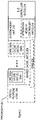
Figure 8 illustrates one embodiment of an interruptcontroller 820 with interruptcontrol logic 821 to forward interrupts to a first core, Core-0 800, or a second core, Core-1 801, of amulti-core processor 810 based on the interrupt sets handled by each core. In the illustrated example, there are 256 interrupts (IRQ0-IRQ255) arranged into six Interrupt Sets 0-6 (e.g., IRQ0-IRQ41 = InterruptSet 1, IRQ42-IRQ83 = InterruptSet 2, etc). It should be noted, however, that the underlying principles of the invention are not limited to any particular number of interrupts or arrangement of interrupt sets. - In one embodiment, each interrupt is associated with an interrupt configuration register (ICR) accessible via an interrupt configuration register interface 822. In
Figure 8 , there are 256 interrupt configuration registers, ICR0-ICR255, one for each of the possible interrupt request lines 0-255. One example of an ICR is described below with respect toFigure 13 (which shows how an interruptconfiguration register 1131 may be programmed to associate its corresponding interrupt with an interrupt domain in accordance with one embodiment of the invention). In the example illustrated inFigure 8 , the interruptcontroller 820 is configured to forward interrupts from Interrupt Set-1, Interrupt Set -2 and Interrupt Set-3 to Core-0 800 and Interrupt Set -4, Interrupt Set-5 and Interrupt Set-6 to Core-1 801. Interrupt set 1 includes interrupts 0-41; interrupt set 2 includes interrupts 42-83; interrupt set 3 includes interrupts 84-127; interrupt set 4 includes interrupts 128-169; interrupt set 5 includes interrupts 170-211; and interrupt set 6 includes interrupts 212-255. - Specific use cases, including those in which one or more Interrupt Sets are required to be reconfigured, are described below.
- As illustrated in
Figure 9 , if the load on Core-0 800 reduces (e.g., below a specified threshold), Interrupt Sets 4-6 on Core-1 801 could be targeted to Core-0 800. Consequently, Core-1 801 may now be put into a switched off state as illustrated (or in another low power state). In this case, the interruptcontroller 820 retargets all Interrupt Sets that were targeted to Core-1 801 to Core-0 800. - In contrast to Use
Case 1, if the load on Core-0 800 exceeds certain limits, it may become beneficial to switch ON Core-1 801. In this scenario, some of the Interrupt Sets may need to be retargeted back to Core-1 801, to achieve a situation similar to that inFigure 8 . - In some implementations, software may decide to migrate the interrupt set from one core to another. For example, if there is an imbalance of load across cores (e.g., because one core is processing a thread consuming significant processor resources), it may be prudent to target one or more Interrupt Sets to those cores that are less loaded. In
Figure 10 , for example, it has been determined that Core-0 800 is more heavily loaded than Core-1 801. As such, the interruptcontroller 820 has retargeted Interrupt Set-1 from Core-0 800 to Core-1 801 to balance the load on both cores. - In all the above use cases, current implementations require each interrupt line to be programmed individually (i.e., one at a time) which significantly increases latency. The latency of programming each interrupt individually can turn out to be a significant bottleneck if the frequency of such reprogramming is high.
- One embodiment of the invention avoids this bottleneck by facilitating atomic programming of an Interrupt Set. In particular, the interrupt
controller 820 can define an optimum number of interrupt domains. In the example provided below, there are 16 interrupt domains among 256 interrupts. It should be noted, however, that the underlying principles of the invention are not limited to any particular number of interrupt domains or interrupts. Each interrupt can be configured to belong to an Interrupt Domain. Such interrupts belonging to an interrupt domain will inherit the properties of that interrupt domain. In one embodiment, one of the properties of each interrupt domain is the destination core to which the interrupts of the interrupt domain should be delivered. Other properties can include, by way of example and not limitation, masking, enabling and disabling of an Interrupt Set. By grouping interrupts into domains and then providing the ability to configure domain properties, only a single configuration operation for each interrupt domain is performed, thereby significantly reducing the latency associated with individual interrupt programming. - As illustrated in
Figure 11A , interruptdomain logic 1150 implemented within the interruptcontroller 820 assigns each of a plurality of interrupt lines 1101-1108 to one of a plurality of interrupt domains 1111-1113. In one embodiment, an interruptconfiguration register 1131 such as shown inFigure 13 includes data specifying the mapping between that particular interrupt line 1101-1108 and an interrupt domain 1111-1113. In the specific example shown, interruptlines domain 1111; interruptlines domain 1112; interruptlines domain 1113. In addition,Figure 11A illustrates that some interrupt lines, such as interruptline 1108, may not be assigned to an interrupt domain. As illustrated, the interruptdomain logic 1150 may operate in an "active mode" for certain interrupt lines 1101-1107, employing interrupt domains 1111-1113 as described, and may operate in a "bypass mode" for those interrupt lines not assigned to a domain. - In one embodiment, each interrupt domain 1111-1113 is configured to send an interrupt to a fixed core or a fixed group of cores. For example, in
Figure 11A interruptdomain 1111 is configured to send interrupts to either Core-0 800 or Core-2 802. Interruptdomain 1112 is configured to send interrupts only to Core-0 800 and interruptdomain 1113 is configured to send interrupts only to Core-1 801. In one embodiment, if the destination core for the interrupts is to be changed, it may be done simply by reprogramming the destination core associated with the interrupt domain (rather than piecemeal programming of each individual interrupt). - As illustrated in the embodiment in
Figure 11B , the interruptcontrol logic 821 includes interruptdomain logic 1150 for processing interrupts in accordance with interrupt domains as described herein. In addition, the interrupt configuration register interface 822 provides the interruptcontroller 820 access to the interrupt domain configuration register(s) (IDCRs) 1130 and interrupt configuration registers (ICR) 1131. As described below, these two sets of registers may be dynamically programmed to assign interrupts to interrupt domains and to assign interrupt domains to cores/processors as described herein. -
Figure 12 illustrates one embodiment of an interrupt domain configuration register comprising entries for 16 programmed interrupt domains (INTDOM_0, INTDOM_1, ... INTDOM_16). In this example, each domain can be configured with a different destination address field (DSTF) which is the address of the destination processor(s)/core(s) to receive interrupts for this domain. For example, in one embodiment, the first 8 bits (D0-D7) of each 64bit IDCR entry comprise DSTF. By way example, and not limitation, the 8bit APIC ID or logical mask of a group of APICs may be programmed in the DSTF. In one embodiment, the DSTF field may encode the logical or the physical address of the LAPIC. - Other fields illustrated in
Figure 12 include a delivery mode (DELM) field which specifies additional parameters for interrupt delivery. In one embodiment, a Fixed delivery mode is specified in which the interrupt signal is delivered to all processor(s)/core(s) specified by the DSTF field. The DELM may also specify Lowest Priority mode in which the interrupt signal is delivered to the processor core that is executing at the lowest priority among all the processors listed in the destination field. Other known interrupt delivery modes may also be implemented. - In one embodiment, the domain destination mode (DSTM) field comprises a 1 bit field which indicates whether physical or logical addressing is used by the interrupt
controller 820. Finally, a domain mask bit indicates whether an interrupt mask is used. In one embodiment, a value of 1 indicates that the interrupt signals in that domain are masked. - Thus, the interrupt domain configuration register(s) 1130 described above allow for atomic programming of an entire interrupt domain. It should be noted, however, that various modifications to the encoding used in the interrupt
domain configuration registers 1130 while still complying with the underlying principles of the invention. -
Figure 13 illustrates one example of how an interruptconfiguration register 1131 may be programmed to associate its corresponding interrupt with an interrupt domain. In particular, a new 4-bit field, Domain ID, is included in the interruptconfiguration register 1131 and may be encoded to identify one of the 16 interrupt domains. An interrupt would thus become a member of the specified interrupt domain. As illustrated inFigure 11A , the ICRs 1131 may be included within and managed by the interruptcontroller 820. In one embodiment, a 1-bit Domain Enable field can be programmed to make the corresponding interrupt a member of an interrupt domain specified by the Domain ID. - Other known fields illustrated in
Figure 13 include an 8-bit Interrupt Vector (INTVEC) field which is a vector number identifying the specific interrupt (e.g., 32 - 255 in the current APIC). All other fields of theICR 1131 are applicable only if EN_INTDOM inICR 1131 is set to 0. A delivery mode (DELM) field may include the same or similar parameters to those described above for the IDCR (e.g., Fixed, Lowest Priority). Similarly, the destination mode (DSTM) bit indicates whether Physical or Logical Addressing of the APIC is used and a destination field (DSTF) is the destination address of the processor to which interrupts belonging to that domain will be delivered to (e.g., the 8bit APIC ID or logical mask of a group of APICs may be programmed here). It should be noted, however, that various modifications to the encoding used in the interruptconfiguration registers 1131 while still complying with the underlying principles of the invention. -
Figure 14 illustrates how the interruptdomain logic 1150 may be implemented in accordance with one embodiment of the invention. Specifically, in the illustrated embodiment, the user programmable interruptconfiguration registers 1131 provide data to adomain ID decoder 1410 and an interrupt configuration switch 1412. The output of thedomain ID decoder 1410 and data from the user programmable interruptdomain configuration registers 1130 are provided to adomain property switch 1411 which responsively updates data contained in an internal shadowdomain configuration register 1401. An interrupt configuration switch 1412 then uses the information from the internal shadowdomain configuration register 1401 and the user programmable interruptconfiguration registers 1131 to generate data into an internal shadow interrupt configuration register 1402, which may be used directly by the interrupt control logic to forward an interrupt to the appropriate core/processor. - In one embodiment, the interrupt
domain logic 1150 operates in two modes: Bypass and Active. When in bypass mode, if the "Domain Enable" bit is disabled in theICR 1131, the interruptcontrol logic 821 will use the interrupt configuration as specified in the ICR. When in active mode, if the "Domain Enable" bit is enabled in theICR 1131, the interruptcontrol logic 821 will use the configuration as specified in theIDCR 1130 corresponding to the Domain ID which may be read from theICR 1131, decoded by thedomain ID decoder 1410, and provided to thedomain property switch 1411. In one embodiment, the interrupt will be delivered only if the domain mask is disabled. - In one embodiment, the
domain ID decoder 1410 is a simple decoder (e.g., a 4:16 bit decoder in the illustrated embodiment) which enables thedomain property switch 1411 to select an appropriate domain configuration. In response to the decoded domain ID, thedomain property switch 1411 selects the configuration of a domain and copies the configuration of the domain into the internal shadowdomain configuration register 1401. - In one embodiment, the interrupt configuration switch 1412 selects the interrupt configuration either from the individual interrupt configuration specified by the ICR 1131 (if the domain is disabled) or from the internal shadow domain configuration register 1401 (if the domain is enabled).
- Thus, if an interrupt is associated with a domain, the domains' configuration will be used to determine the actions related to that interrupt.
- The following pseudo-code shows an example of reconfiguring interrupts with and without interrupt domains.
-
 processor_id = 0x1; /* New Destination adress */
 dst_addr_pos = 60; /* Bit position of the destination address */
 interrupt_ids[] = {0 , 10 , 12 , 15 , 20) /* Example list of interrupt IDs * /
 void reconfigure_interrupts (unsigned int num_ interrupts, unsigned int * interrupt_ids
 , unsigned int processor_id)
 {
      X = disable_interrupts( ); /∗ disable at global level ∗/
      {
      ICR[interrupt ids [0]] = processor id<<dst_addr_pos | ICR[interrupt_ ids[0]];
      /∗ ICR [0]∗/
      ICR[interrupt ids [1]] = processor id<<dst_addr_pos | ICR[interrupt_ ids[1]];
      /∗ ICR [10]∗/
      ICR[interrupt ids [2]] = processor id<<dst_addr_pos | ICR[interrupt_ ids[2]];
      /∗ ICR [12]∗/
      ICR[interrupt ids [3]] = processor id<<dst_addr_pos | ICR[interrupt_ ids[3]];
      /∗ ICR [15]∗/
      ICR[interrupt ids [4]] = processor id<<dst_addr_pos | ICR[interrupt_ ids[4]];
      /∗ ICR [20]∗/
      }
 enable_interrupts (X) ; /∗ enable at global level ∗/
The computing time of the above is O(n) where n is number of interrupts to be reconfigured.
 domain_id = 0 ; /∗ Domain id that is to be reconfigured ∗/
 processor id 0x1; /∗ New Destination address ∗/
 dst_addr_pos = 60; /∗ Bit position of the destination address ∗/
 void reconfigure_interruptdomain (unsigned int domain_id, unsigned int
 processor_id)
 {
      X = disable interrupts(); /∗ disable at global or domain level ∗/
 IDCR[domain_id] = processor_ id<< dst_ addr_pos | IDCR[domain_ id]; /∗ ONLY
 ONE REGISTER WRITE ! ∗/
      enable_ interrupts (X); /∗ enable at global or domain level ∗/
 }
Claims (10)
- An apparatus comprising:a plurality of cores (800, 801, 802); andan interrupt controller (820) configured to group interrupts into a plurality of interrupt domains (1111 - 1113), each interrupt domain configured to have a set of interrupts assigned thereto and to map the interrupts in the set to one or more destination cores of the plurality of cores (800, 801, 802),in response to arrival of a new interrupt, the interrupt controller is configured to consult the interrupt domain to identify a core to process the new interrupt; andcharacterized in that upon a reassignment event comprising a processing load on one or more of the processor cores reaching a specified threshold or being higher than processing load on one or more other cores by a threshold difference in processing load, the interrupt controller (820) is configured to dynamically reassign the one or more interrupt domains (1111 - 1113) from the core with the relatively greater processing load to one or more cores with relatively lower processing load.
- The apparatus as in claim 1 further comprising:
one or more interrupt domain configuration registers, IDCRs, (1130) comprising an entry for each of the interrupt domains, each entry configured to include a Destination Address to identify one or more cores to service the interrupts assigned to each respective interrupt domain (1111 - 1113). - The apparatus as in claim 2 wherein the Destination Address field comprises a configurable field in accordance with a processor architecture and the associated interrupt controller.
- The apparatus as in claim 2 further comprising:
one or more interrupt configuration registers, ICR0 - ICR255, comprising an entry for each interrupt, each entry to include an interrupt domain field to identify an interrupt domain to which the interrupt is assigned. - The apparatus as in claim 2 wherein each entry in the IDCRs is configured to further include a Delivery Mode field to specify one or more additional parameters for interrupt delivery, a Domain Mask to specify whether the interrupt is to be assigned to a domain and a destination mode to specify whether a physical or a logical addressing mode is to be used.
- The apparatus as in claim 1 wherein the reassignment event comprises one of the cores entering into a low power state, wherein the interrupt controller is configured to reassign interrupt domains from the core entering into the low power state to one or more other cores.
- A method comprising:grouping interrupts into a plurality of interrupt domains, each interrupt domain having a set of interrupts assigned thereto and mapping the interrupts in the set to one or more destination cores of a plurality of cores of a processor;receiving, by an interrupt controller, a new interrupt;responsively determining, by the interrupt controller, an interrupt domain to which the new interrupt is assigned to identify a core associated with the interrupt domain; andforwarding, by the interrupt controller, the interrupt to the core associated with the interrupt domain;characterized in that the method further comprises:detecting that a processing load on one or more of the processor cores has reached a specified threshold; anddynamically reassigning the one or more interrupt domains from the core with the relatively greater processing load to one or more cores with relatively lower processing load.
- The method as in claim 7 wherein identifying a core comprises reading one or more interrupt domain configuration registers, IDCRs, comprising an entry for each of the interrupt domains, each entry comprising a Destination Address to identify one or more cores to service the interrupts assigned to the interrupt domain.
- The method as in claim 8 wherein the Destination Address field comprises a configurable field in accordance with a processor architecture and the associated interrupt controller.
- The method as in claim 8 wherein determining an interrupt domain further comprises:
reading one or more interrupt configuration registers comprising an entry for each interrupt, each entry to include an interrupt domain field to identify an interrupt domain to which the interrupt is assigned.
Priority Applications (1)
| Application Number | Priority Date | Filing Date | Title |
|---|---|---|---|
| EP20217471.0A EP3855318B1 (en) | 2014-09-26 | 2015-09-10 | Apparatus and method for configuring sets of interrupts |
Applications Claiming Priority (2)
| Application Number | Priority Date | Filing Date | Title |
|---|---|---|---|
| IN4721CH2014 | 2014-09-26 | ||
| PCT/US2015/049337 WO2016048669A1 (en) | 2014-09-26 | 2015-09-10 | Apparatus and method for configuring sets of interrupts |
Related Child Applications (2)
| Application Number | Title | Priority Date | Filing Date |
|---|---|---|---|
| EP20217471.0A Division EP3855318B1 (en) | 2014-09-26 | 2015-09-10 | Apparatus and method for configuring sets of interrupts |
| EP20217471.0A Division-Into EP3855318B1 (en) | 2014-09-26 | 2015-09-10 | Apparatus and method for configuring sets of interrupts |
Publications (3)
| Publication Number | Publication Date |
|---|---|
| EP3198460A1 EP3198460A1 (en) | 2017-08-02 |
| EP3198460A4 EP3198460A4 (en) | 2018-05-02 |
| EP3198460B1 true EP3198460B1 (en) | 2022-08-17 |
Family
ID=55581805
Family Applications (2)
| Application Number | Title | Priority Date | Filing Date |
|---|---|---|---|
| EP20217471.0A Active EP3855318B1 (en) | 2014-09-26 | 2015-09-10 | Apparatus and method for configuring sets of interrupts |
| EP15844406.7A Active EP3198460B1 (en) | 2014-09-26 | 2015-09-10 | Apparatus and method for configuring sets of interrupts |
Family Applications Before (1)
| Application Number | Title | Priority Date | Filing Date |
|---|---|---|---|
| EP20217471.0A Active EP3855318B1 (en) | 2014-09-26 | 2015-09-10 | Apparatus and method for configuring sets of interrupts |
Country Status (7)
| Country | Link |
|---|---|
| US (5) | US10296335B2 (en) |
| EP (2) | EP3855318B1 (en) |
| KR (2) | KR102187912B1 (en) |
| CN (2) | CN106663072B (en) |
| ES (1) | ES2929512T3 (en) |
| PL (1) | PL3198460T3 (en) |
| WO (1) | WO2016048669A1 (en) |
Families Citing this family (10)
| Publication number | Priority date | Publication date | Assignee | Title |
|---|---|---|---|---|
| FR3061565B1 (en) | 2017-01-04 | 2019-04-26 | Stmicroelectronics (Rousset) Sas | OPERATION OF A MICROCONTROLLER IN LOW POWER MODE |
| US10540736B2 (en) * | 2017-08-03 | 2020-01-21 | Texas Instruments Incorporated | Display sub-system sharing for heterogeneous systems |
| US10838760B2 (en) * | 2017-11-29 | 2020-11-17 | Nxp Usa, Inc. | Systems and methods for interrupt distribution |
| US11630789B2 (en) * | 2020-09-11 | 2023-04-18 | Apple Inc. | Scalable interrupts |
| CN112181877B (en) * | 2020-10-28 | 2022-06-21 | 瑞芯微电子股份有限公司 | Display frequency conversion method and system |
| CN112416536B (en) * | 2020-12-10 | 2023-08-18 | 成都海光集成电路设计有限公司 | Method for extracting processor execution context and processor |
| CN113238802A (en) * | 2021-05-28 | 2021-08-10 | 上海阵量智能科技有限公司 | Interrupt distributor, data processing chip, interrupt distribution method and data processing method |
| US20230053530A1 (en) | 2021-08-23 | 2023-02-23 | Apple Inc. | Scalable System on a Chip |
| CN113918311B (en) * | 2021-12-10 | 2022-07-01 | 北京智芯微电子科技有限公司 | Soft interrupt routing method of multi-core system and method and chip for responding soft interrupt |
| CN116821026B (en) * | 2023-08-28 | 2023-11-24 | 麒麟软件有限公司 | LPC bus parallel port conversion method and system under ARM architecture |
Family Cites Families (14)
| Publication number | Priority date | Publication date | Assignee | Title |
|---|---|---|---|---|
| US5535420A (en) * | 1994-12-14 | 1996-07-09 | Intel Corporation | Method and apparatus for interrupt signaling in a computer system |
| US7584316B2 (en) * | 2003-10-14 | 2009-09-01 | Broadcom Corporation | Packet manager interrupt mapper |
| US20080126652A1 (en) * | 2006-09-27 | 2008-05-29 | Intel Corporation | Managing Interrupts in a Partitioned Platform |
| US7962679B2 (en) * | 2007-09-28 | 2011-06-14 | Intel Corporation | Interrupt balancing for multi-core and power |
| US7962771B2 (en) * | 2007-12-31 | 2011-06-14 | Intel Corporation | Method, system, and apparatus for rerouting interrupts in a multi-core processor |
| CN101354664B (en) * | 2008-08-19 | 2011-12-28 | 中兴通讯股份有限公司 | Method and apparatus for interrupting load equilibrium of multi-core processor |
| US8321614B2 (en) * | 2009-04-24 | 2012-11-27 | Empire Technology Development Llc | Dynamic scheduling interrupt controller for multiprocessors |
| US8356130B2 (en) * | 2009-08-14 | 2013-01-15 | Advanced Micro Devices, Inc. | Mechanism for recording undeliverable user-level interrupts |
| CN102063335B (en) * | 2009-11-13 | 2014-04-02 | 大唐移动通信设备有限公司 | Interrupt controller and method for processing interrupt of multi-core processor shared device |
| CN101901165B (en) * | 2010-07-26 | 2013-04-10 | 清华大学 | Circuit structure of interruption controller |
| US8738860B1 (en) * | 2010-10-25 | 2014-05-27 | Tilera Corporation | Computing in parallel processing environments |
| US8959270B2 (en) * | 2010-12-07 | 2015-02-17 | Apple Inc. | Interrupt distribution scheme |
| US10990407B2 (en) * | 2012-04-24 | 2021-04-27 | Intel Corporation | Dynamic interrupt reconfiguration for effective power management |
| WO2013162589A1 (en) * | 2012-04-27 | 2013-10-31 | Intel Corporation | Migrating tasks between asymmetric computing elements of a multi-core processor |
-
2015
- 2015-09-10 CN CN201580045622.9A patent/CN106663072B/en active Active
- 2015-09-10 WO PCT/US2015/049337 patent/WO2016048669A1/en active Application Filing
- 2015-09-10 EP EP20217471.0A patent/EP3855318B1/en active Active
- 2015-09-10 KR KR1020177005138A patent/KR102187912B1/en active IP Right Grant
- 2015-09-10 CN CN202011165638.2A patent/CN112698928A/en active Pending
- 2015-09-10 EP EP15844406.7A patent/EP3198460B1/en active Active
- 2015-09-10 PL PL15844406.7T patent/PL3198460T3/en unknown
- 2015-09-10 ES ES15844406T patent/ES2929512T3/en active Active
- 2015-09-10 KR KR1020207034588A patent/KR102309327B1/en active IP Right Grant
- 2015-09-22 US US14/861,618 patent/US10296335B2/en active Active
-
2019
- 2019-01-23 US US16/255,438 patent/US10936313B2/en active Active
-
2021
- 2021-01-27 US US17/159,415 patent/US11500633B2/en active Active
-
2022
- 2022-11-08 US US17/982,794 patent/US11740902B2/en active Active
-
2023
- 2023-07-05 US US18/218,119 patent/US20240004651A1/en active Pending
Also Published As
| Publication number | Publication date |
|---|---|
| CN106663072A (en) | 2017-05-10 |
| EP3855318B1 (en) | 2024-02-14 |
| KR20170036035A (en) | 2017-03-31 |
| EP3855318A1 (en) | 2021-07-28 |
| EP3198460A1 (en) | 2017-08-02 |
| KR102187912B1 (en) | 2020-12-07 |
| KR102309327B1 (en) | 2021-10-07 |
| US20240004651A1 (en) | 2024-01-04 |
| PL3198460T3 (en) | 2022-11-14 |
| US20160196141A1 (en) | 2016-07-07 |
| US20210255865A1 (en) | 2021-08-19 |
| US10296335B2 (en) | 2019-05-21 |
| US10936313B2 (en) | 2021-03-02 |
| EP3198460A4 (en) | 2018-05-02 |
| US20230070764A1 (en) | 2023-03-09 |
| CN112698928A (en) | 2021-04-23 |
| CN106663072B (en) | 2020-11-17 |
| KR20200138439A (en) | 2020-12-09 |
| ES2929512T3 (en) | 2022-11-29 |
| US11500633B2 (en) | 2022-11-15 |
| US11740902B2 (en) | 2023-08-29 |
| US20200004537A1 (en) | 2020-01-02 |
| WO2016048669A1 (en) | 2016-03-31 |
Similar Documents
| Publication | Publication Date | Title |
|---|---|---|
| US11500633B2 (en) | Apparatus and method for configuring sets of interrupts | |
| EP2831693B1 (en) | Apparatus and method for accelerating operations in a processor which uses shared virtual memory | |
| US11243768B2 (en) | Mechanism for saving and retrieving micro-architecture context | |
| CN105144082B (en) | Optimal logical processor count and type selection for a given workload based on platform thermal and power budget constraints | |
| US10127039B2 (en) | Extension of CPU context-state management for micro-architecture state | |
| US20210232426A1 (en) | Apparatus, method, and system for ensuring quality of service for multi-threading processor cores | |
| US20180365022A1 (en) | Dynamic offlining and onlining of processor cores | |
| WO2014105151A1 (en) | Apparatus and method for a multiple page size translation lookaside buffer (tlb) | |
| US9983880B2 (en) | Method and apparatus for improved thread selection | |
| US11775336B2 (en) | Apparatus and method for performance state matching between source and target processors based on interprocessor interrupts | |
| US11907712B2 (en) | Methods, systems, and apparatuses for out-of-order access to a shared microcode sequencer by a clustered decode pipeline | |
| US20220100569A1 (en) | Methods, systems, and apparatuses for scalable port-binding for asymmetric execution ports and allocation widths of a processor | |
| EP4202664A1 (en) | System, apparatus and method for throttling fusion of micro-operations in a processor | |
| US20180349137A1 (en) | Reconfiguring a processor without a system reset | |
| CN116339971A (en) | Dynamic asymmetric resources |
Legal Events
| Date | Code | Title | Description |
|---|---|---|---|
| STAA | Information on the status of an ep patent application or granted ep patent |
Free format text: STATUS: THE INTERNATIONAL PUBLICATION HAS BEEN MADE |
|
| PUAI | Public reference made under article 153(3) epc to a published international application that has entered the european phase |
Free format text: ORIGINAL CODE: 0009012 |
|
| STAA | Information on the status of an ep patent application or granted ep patent |
Free format text: STATUS: REQUEST FOR EXAMINATION WAS MADE |
|
| 17P | Request for examination filed |
Effective date: 20170301 |
|
| AK | Designated contracting states |
Kind code of ref document: A1 Designated state(s): AL AT BE BG CH CY CZ DE DK EE ES FI FR GB GR HR HU IE IS IT LI LT LU LV MC MK MT NL NO PL PT RO RS SE SI SK SM TR |
|
| AX | Request for extension of the european patent |
Extension state: BA ME |
|
| DAV | Request for validation of the european patent (deleted) | ||
| DAX | Request for extension of the european patent (deleted) | ||
| A4 | Supplementary search report drawn up and despatched |
Effective date: 20180406 |
|
| RIC1 | Information provided on ipc code assigned before grant |
Ipc: G06F 9/50 20060101ALI20180329BHEP Ipc: G06F 13/24 20060101AFI20180329BHEP Ipc: G06F 9/48 20060101ALI20180329BHEP |
|
| STAA | Information on the status of an ep patent application or granted ep patent |
Free format text: STATUS: EXAMINATION IS IN PROGRESS |
|
| 17Q | First examination report despatched |
Effective date: 20210325 |
|
| GRAP | Despatch of communication of intention to grant a patent |
Free format text: ORIGINAL CODE: EPIDOSNIGR1 |
|
| STAA | Information on the status of an ep patent application or granted ep patent |
Free format text: STATUS: GRANT OF PATENT IS INTENDED |
|
| INTG | Intention to grant announced |
Effective date: 20211026 |
|
| GRAJ | Information related to disapproval of communication of intention to grant by the applicant or resumption of examination proceedings by the epo deleted |
Free format text: ORIGINAL CODE: EPIDOSDIGR1 |
|
| STAA | Information on the status of an ep patent application or granted ep patent |
Free format text: STATUS: EXAMINATION IS IN PROGRESS |
|
| GRAP | Despatch of communication of intention to grant a patent |
Free format text: ORIGINAL CODE: EPIDOSNIGR1 |
|
| STAA | Information on the status of an ep patent application or granted ep patent |
Free format text: STATUS: GRANT OF PATENT IS INTENDED |
|
| INTC | Intention to grant announced (deleted) | ||
| INTG | Intention to grant announced |
Effective date: 20220318 |
|
| GRAS | Grant fee paid |
Free format text: ORIGINAL CODE: EPIDOSNIGR3 |
|
| GRAA | (expected) grant |
Free format text: ORIGINAL CODE: 0009210 |
|
| STAA | Information on the status of an ep patent application or granted ep patent |
Free format text: STATUS: THE PATENT HAS BEEN GRANTED |
|
| AK | Designated contracting states |
Kind code of ref document: B1 Designated state(s): AL AT BE BG CH CY CZ DE DK EE ES FI FR GB GR HR HU IE IS IT LI LT LU LV MC MK MT NL NO PL PT RO RS SE SI SK SM TR |
|
| REG | Reference to a national code |
Ref country code: CH Ref legal event code: EP |
|
| REG | Reference to a national code |
Ref country code: DE Ref legal event code: R096 Ref document number: 602015080409 Country of ref document: DE |
|
| REG | Reference to a national code |
Ref country code: IE Ref legal event code: FG4D |
|
| REG | Reference to a national code |
Ref country code: AT Ref legal event code: REF Ref document number: 1512635 Country of ref document: AT Kind code of ref document: T Effective date: 20220915 |
|
| REG | Reference to a national code |
Ref country code: NL Ref legal event code: FP |
|
| REG | Reference to a national code |
Ref country code: ES Ref legal event code: FG2A Ref document number: 2929512 Country of ref document: ES Kind code of ref document: T3 Effective date: 20221129 |
|
| REG | Reference to a national code |
Ref country code: LT Ref legal event code: MG9D |
|
| PG25 | Lapsed in a contracting state [announced via postgrant information from national office to epo] |
Ref country code: SE Free format text: LAPSE BECAUSE OF FAILURE TO SUBMIT A TRANSLATION OF THE DESCRIPTION OR TO PAY THE FEE WITHIN THE PRESCRIBED TIME-LIMIT Effective date: 20220817 Ref country code: RS Free format text: LAPSE BECAUSE OF FAILURE TO SUBMIT A TRANSLATION OF THE DESCRIPTION OR TO PAY THE FEE WITHIN THE PRESCRIBED TIME-LIMIT Effective date: 20220817 Ref country code: PT Free format text: LAPSE BECAUSE OF FAILURE TO SUBMIT A TRANSLATION OF THE DESCRIPTION OR TO PAY THE FEE WITHIN THE PRESCRIBED TIME-LIMIT Effective date: 20221219 Ref country code: NO Free format text: LAPSE BECAUSE OF FAILURE TO SUBMIT A TRANSLATION OF THE DESCRIPTION OR TO PAY THE FEE WITHIN THE PRESCRIBED TIME-LIMIT Effective date: 20221117 Ref country code: LV Free format text: LAPSE BECAUSE OF FAILURE TO SUBMIT A TRANSLATION OF THE DESCRIPTION OR TO PAY THE FEE WITHIN THE PRESCRIBED TIME-LIMIT Effective date: 20220817 Ref country code: LT Free format text: LAPSE BECAUSE OF FAILURE TO SUBMIT A TRANSLATION OF THE DESCRIPTION OR TO PAY THE FEE WITHIN THE PRESCRIBED TIME-LIMIT Effective date: 20220817 Ref country code: FI Free format text: LAPSE BECAUSE OF FAILURE TO SUBMIT A TRANSLATION OF THE DESCRIPTION OR TO PAY THE FEE WITHIN THE PRESCRIBED TIME-LIMIT Effective date: 20220817 |
|
| REG | Reference to a national code |
Ref country code: AT Ref legal event code: MK05 Ref document number: 1512635 Country of ref document: AT Kind code of ref document: T Effective date: 20220817 |
|
| PG25 | Lapsed in a contracting state [announced via postgrant information from national office to epo] |
Ref country code: IS Free format text: LAPSE BECAUSE OF FAILURE TO SUBMIT A TRANSLATION OF THE DESCRIPTION OR TO PAY THE FEE WITHIN THE PRESCRIBED TIME-LIMIT Effective date: 20221217 Ref country code: HR Free format text: LAPSE BECAUSE OF FAILURE TO SUBMIT A TRANSLATION OF THE DESCRIPTION OR TO PAY THE FEE WITHIN THE PRESCRIBED TIME-LIMIT Effective date: 20220817 Ref country code: GR Free format text: LAPSE BECAUSE OF FAILURE TO SUBMIT A TRANSLATION OF THE DESCRIPTION OR TO PAY THE FEE WITHIN THE PRESCRIBED TIME-LIMIT Effective date: 20221118 |
|
| PG25 | Lapsed in a contracting state [announced via postgrant information from national office to epo] |
Ref country code: SM Free format text: LAPSE BECAUSE OF FAILURE TO SUBMIT A TRANSLATION OF THE DESCRIPTION OR TO PAY THE FEE WITHIN THE PRESCRIBED TIME-LIMIT Effective date: 20220817 Ref country code: RO Free format text: LAPSE BECAUSE OF FAILURE TO SUBMIT A TRANSLATION OF THE DESCRIPTION OR TO PAY THE FEE WITHIN THE PRESCRIBED TIME-LIMIT Effective date: 20220817 Ref country code: DK Free format text: LAPSE BECAUSE OF FAILURE TO SUBMIT A TRANSLATION OF THE DESCRIPTION OR TO PAY THE FEE WITHIN THE PRESCRIBED TIME-LIMIT Effective date: 20220817 Ref country code: CZ Free format text: LAPSE BECAUSE OF FAILURE TO SUBMIT A TRANSLATION OF THE DESCRIPTION OR TO PAY THE FEE WITHIN THE PRESCRIBED TIME-LIMIT Effective date: 20220817 Ref country code: AT Free format text: LAPSE BECAUSE OF FAILURE TO SUBMIT A TRANSLATION OF THE DESCRIPTION OR TO PAY THE FEE WITHIN THE PRESCRIBED TIME-LIMIT Effective date: 20220817 |
|
| REG | Reference to a national code |
Ref country code: CH Ref legal event code: PL |
|
| REG | Reference to a national code |
Ref country code: DE Ref legal event code: R097 Ref document number: 602015080409 Country of ref document: DE |
|
| REG | Reference to a national code |
Ref country code: BE Ref legal event code: MM Effective date: 20220930 |
|
| PG25 | Lapsed in a contracting state [announced via postgrant information from national office to epo] |
Ref country code: SK Free format text: LAPSE BECAUSE OF FAILURE TO SUBMIT A TRANSLATION OF THE DESCRIPTION OR TO PAY THE FEE WITHIN THE PRESCRIBED TIME-LIMIT Effective date: 20220817 Ref country code: MC Free format text: LAPSE BECAUSE OF FAILURE TO SUBMIT A TRANSLATION OF THE DESCRIPTION OR TO PAY THE FEE WITHIN THE PRESCRIBED TIME-LIMIT Effective date: 20220817 Ref country code: EE Free format text: LAPSE BECAUSE OF FAILURE TO SUBMIT A TRANSLATION OF THE DESCRIPTION OR TO PAY THE FEE WITHIN THE PRESCRIBED TIME-LIMIT Effective date: 20220817 |
|
| P01 | Opt-out of the competence of the unified patent court (upc) registered |
Effective date: 20230518 |
|
| PLBE | No opposition filed within time limit |
Free format text: ORIGINAL CODE: 0009261 |
|
| STAA | Information on the status of an ep patent application or granted ep patent |
Free format text: STATUS: NO OPPOSITION FILED WITHIN TIME LIMIT |
|
| PG25 | Lapsed in a contracting state [announced via postgrant information from national office to epo] |
Ref country code: LU Free format text: LAPSE BECAUSE OF NON-PAYMENT OF DUE FEES Effective date: 20220910 Ref country code: AL Free format text: LAPSE BECAUSE OF FAILURE TO SUBMIT A TRANSLATION OF THE DESCRIPTION OR TO PAY THE FEE WITHIN THE PRESCRIBED TIME-LIMIT Effective date: 20220817 |
|
| 26N | No opposition filed |
Effective date: 20230519 |
|
| PG25 | Lapsed in a contracting state [announced via postgrant information from national office to epo] |
Ref country code: LI Free format text: LAPSE BECAUSE OF NON-PAYMENT OF DUE FEES Effective date: 20220930 Ref country code: IE Free format text: LAPSE BECAUSE OF NON-PAYMENT OF DUE FEES Effective date: 20220910 Ref country code: CH Free format text: LAPSE BECAUSE OF NON-PAYMENT OF DUE FEES Effective date: 20220930 |
|
| PG25 | Lapsed in a contracting state [announced via postgrant information from national office to epo] |
Ref country code: SI Free format text: LAPSE BECAUSE OF FAILURE TO SUBMIT A TRANSLATION OF THE DESCRIPTION OR TO PAY THE FEE WITHIN THE PRESCRIBED TIME-LIMIT Effective date: 20220817 |
|
| PG25 | Lapsed in a contracting state [announced via postgrant information from national office to epo] |
Ref country code: BE Free format text: LAPSE BECAUSE OF NON-PAYMENT OF DUE FEES Effective date: 20220930 |
|
| PGFP | Annual fee paid to national office [announced via postgrant information from national office to epo] |
Ref country code: NL Payment date: 20230825 Year of fee payment: 9 |
|
| PG25 | Lapsed in a contracting state [announced via postgrant information from national office to epo] |
Ref country code: IT Free format text: LAPSE BECAUSE OF NON-PAYMENT OF DUE FEES Effective date: 20220910 |
|
| PGFP | Annual fee paid to national office [announced via postgrant information from national office to epo] |
Ref country code: GB Payment date: 20230817 Year of fee payment: 9 |
|
| PGFP | Annual fee paid to national office [announced via postgrant information from national office to epo] |
Ref country code: PL Payment date: 20230830 Year of fee payment: 9 Ref country code: FR Payment date: 20230821 Year of fee payment: 9 Ref country code: DE Payment date: 20230822 Year of fee payment: 9 |
|
| PGFP | Annual fee paid to national office [announced via postgrant information from national office to epo] |
Ref country code: ES Payment date: 20231005 Year of fee payment: 9 |
|
| PG25 | Lapsed in a contracting state [announced via postgrant information from national office to epo] |
Ref country code: HU Free format text: LAPSE BECAUSE OF FAILURE TO SUBMIT A TRANSLATION OF THE DESCRIPTION OR TO PAY THE FEE WITHIN THE PRESCRIBED TIME-LIMIT; INVALID AB INITIO Effective date: 20150910 |