EP3197243A1 - White light emitting organic el panel and method for producing same - Google Patents
White light emitting organic el panel and method for producing same Download PDFInfo
- Publication number
- EP3197243A1 EP3197243A1 EP16821110.0A EP16821110A EP3197243A1 EP 3197243 A1 EP3197243 A1 EP 3197243A1 EP 16821110 A EP16821110 A EP 16821110A EP 3197243 A1 EP3197243 A1 EP 3197243A1
- Authority
- EP
- European Patent Office
- Prior art keywords
- light
- emitting
- layer
- red
- green
- Prior art date
- Legal status (The legal status is an assumption and is not a legal conclusion. Google has not performed a legal analysis and makes no representation as to the accuracy of the status listed.)
- Granted
Links
Images



Classifications
-
- C—CHEMISTRY; METALLURGY
- C09—DYES; PAINTS; POLISHES; NATURAL RESINS; ADHESIVES; COMPOSITIONS NOT OTHERWISE PROVIDED FOR; APPLICATIONS OF MATERIALS NOT OTHERWISE PROVIDED FOR
- C09K—MATERIALS FOR MISCELLANEOUS APPLICATIONS, NOT PROVIDED FOR ELSEWHERE
- C09K11/00—Luminescent materials, e.g. electroluminescent or chemiluminescent
- C09K11/06—Luminescent materials, e.g. electroluminescent or chemiluminescent containing organic luminescent materials
-
- H—ELECTRICITY
- H10—SEMICONDUCTOR DEVICES; ELECTRIC SOLID-STATE DEVICES NOT OTHERWISE PROVIDED FOR
- H10K—ORGANIC ELECTRIC SOLID-STATE DEVICES
- H10K50/00—Organic light-emitting devices
-
- H—ELECTRICITY
- H10—SEMICONDUCTOR DEVICES; ELECTRIC SOLID-STATE DEVICES NOT OTHERWISE PROVIDED FOR
- H10K—ORGANIC ELECTRIC SOLID-STATE DEVICES
- H10K50/00—Organic light-emitting devices
- H10K50/10—OLEDs or polymer light-emitting diodes [PLED]
- H10K50/11—OLEDs or polymer light-emitting diodes [PLED] characterised by the electroluminescent [EL] layers
-
- H—ELECTRICITY
- H10—SEMICONDUCTOR DEVICES; ELECTRIC SOLID-STATE DEVICES NOT OTHERWISE PROVIDED FOR
- H10K—ORGANIC ELECTRIC SOLID-STATE DEVICES
- H10K50/00—Organic light-emitting devices
- H10K50/10—OLEDs or polymer light-emitting diodes [PLED]
- H10K50/11—OLEDs or polymer light-emitting diodes [PLED] characterised by the electroluminescent [EL] layers
- H10K50/125—OLEDs or polymer light-emitting diodes [PLED] characterised by the electroluminescent [EL] layers specially adapted for multicolour light emission, e.g. for emitting white light
-
- H—ELECTRICITY
- H10—SEMICONDUCTOR DEVICES; ELECTRIC SOLID-STATE DEVICES NOT OTHERWISE PROVIDED FOR
- H10K—ORGANIC ELECTRIC SOLID-STATE DEVICES
- H10K50/00—Organic light-emitting devices
- H10K50/10—OLEDs or polymer light-emitting diodes [PLED]
- H10K50/11—OLEDs or polymer light-emitting diodes [PLED] characterised by the electroluminescent [EL] layers
- H10K50/125—OLEDs or polymer light-emitting diodes [PLED] characterised by the electroluminescent [EL] layers specially adapted for multicolour light emission, e.g. for emitting white light
- H10K50/13—OLEDs or polymer light-emitting diodes [PLED] characterised by the electroluminescent [EL] layers specially adapted for multicolour light emission, e.g. for emitting white light comprising stacked EL layers within one EL unit
- H10K50/131—OLEDs or polymer light-emitting diodes [PLED] characterised by the electroluminescent [EL] layers specially adapted for multicolour light emission, e.g. for emitting white light comprising stacked EL layers within one EL unit with spacer layers between the electroluminescent layers
-
- H—ELECTRICITY
- H10—SEMICONDUCTOR DEVICES; ELECTRIC SOLID-STATE DEVICES NOT OTHERWISE PROVIDED FOR
- H10K—ORGANIC ELECTRIC SOLID-STATE DEVICES
- H10K50/00—Organic light-emitting devices
- H10K50/80—Constructional details
- H10K50/805—Electrodes
- H10K50/81—Anodes
-
- H—ELECTRICITY
- H10—SEMICONDUCTOR DEVICES; ELECTRIC SOLID-STATE DEVICES NOT OTHERWISE PROVIDED FOR
- H10K—ORGANIC ELECTRIC SOLID-STATE DEVICES
- H10K50/00—Organic light-emitting devices
- H10K50/80—Constructional details
- H10K50/805—Electrodes
- H10K50/82—Cathodes
-
- H—ELECTRICITY
- H10—SEMICONDUCTOR DEVICES; ELECTRIC SOLID-STATE DEVICES NOT OTHERWISE PROVIDED FOR
- H10K—ORGANIC ELECTRIC SOLID-STATE DEVICES
- H10K50/00—Organic light-emitting devices
- H10K50/80—Constructional details
- H10K50/84—Passivation; Containers; Encapsulations
- H10K50/841—Self-supporting sealing arrangements
-
- H—ELECTRICITY
- H10—SEMICONDUCTOR DEVICES; ELECTRIC SOLID-STATE DEVICES NOT OTHERWISE PROVIDED FOR
- H10K—ORGANIC ELECTRIC SOLID-STATE DEVICES
- H10K59/00—Integrated devices, or assemblies of multiple devices, comprising at least one organic light-emitting element covered by group H10K50/00
- H10K59/80—Constructional details
- H10K59/87—Passivation; Containers; Encapsulations
- H10K59/871—Self-supporting sealing arrangements
-
- H—ELECTRICITY
- H10—SEMICONDUCTOR DEVICES; ELECTRIC SOLID-STATE DEVICES NOT OTHERWISE PROVIDED FOR
- H10K—ORGANIC ELECTRIC SOLID-STATE DEVICES
- H10K71/00—Manufacture or treatment specially adapted for the organic devices covered by this subclass
-
- H—ELECTRICITY
- H10—SEMICONDUCTOR DEVICES; ELECTRIC SOLID-STATE DEVICES NOT OTHERWISE PROVIDED FOR
- H10K—ORGANIC ELECTRIC SOLID-STATE DEVICES
- H10K71/00—Manufacture or treatment specially adapted for the organic devices covered by this subclass
- H10K71/10—Deposition of organic active material
- H10K71/16—Deposition of organic active material using physical vapour deposition [PVD], e.g. vacuum deposition or sputtering
- H10K71/164—Deposition of organic active material using physical vapour deposition [PVD], e.g. vacuum deposition or sputtering using vacuum deposition
-
- H—ELECTRICITY
- H10—SEMICONDUCTOR DEVICES; ELECTRIC SOLID-STATE DEVICES NOT OTHERWISE PROVIDED FOR
- H10K—ORGANIC ELECTRIC SOLID-STATE DEVICES
- H10K77/00—Constructional details of devices covered by this subclass and not covered by groups H10K10/80, H10K30/80, H10K50/80 or H10K59/80
- H10K77/10—Substrates, e.g. flexible substrates
-
- C—CHEMISTRY; METALLURGY
- C09—DYES; PAINTS; POLISHES; NATURAL RESINS; ADHESIVES; COMPOSITIONS NOT OTHERWISE PROVIDED FOR; APPLICATIONS OF MATERIALS NOT OTHERWISE PROVIDED FOR
- C09K—MATERIALS FOR MISCELLANEOUS APPLICATIONS, NOT PROVIDED FOR ELSEWHERE
- C09K2211/00—Chemical nature of organic luminescent or tenebrescent compounds
- C09K2211/18—Metal complexes
- C09K2211/185—Metal complexes of the platinum group, i.e. Os, Ir, Pt, Ru, Rh or Pd
-
- H—ELECTRICITY
- H10—SEMICONDUCTOR DEVICES; ELECTRIC SOLID-STATE DEVICES NOT OTHERWISE PROVIDED FOR
- H10K—ORGANIC ELECTRIC SOLID-STATE DEVICES
- H10K2101/00—Properties of the organic materials covered by group H10K85/00
- H10K2101/10—Triplet emission
-
- H—ELECTRICITY
- H10—SEMICONDUCTOR DEVICES; ELECTRIC SOLID-STATE DEVICES NOT OTHERWISE PROVIDED FOR
- H10K—ORGANIC ELECTRIC SOLID-STATE DEVICES
- H10K2101/00—Properties of the organic materials covered by group H10K85/00
- H10K2101/30—Highest occupied molecular orbital [HOMO], lowest unoccupied molecular orbital [LUMO] or Fermi energy values
-
- H—ELECTRICITY
- H10—SEMICONDUCTOR DEVICES; ELECTRIC SOLID-STATE DEVICES NOT OTHERWISE PROVIDED FOR
- H10K—ORGANIC ELECTRIC SOLID-STATE DEVICES
- H10K2101/00—Properties of the organic materials covered by group H10K85/00
- H10K2101/40—Interrelation of parameters between multiple constituent active layers or sublayers, e.g. HOMO values in adjacent layers
-
- H—ELECTRICITY
- H10—SEMICONDUCTOR DEVICES; ELECTRIC SOLID-STATE DEVICES NOT OTHERWISE PROVIDED FOR
- H10K—ORGANIC ELECTRIC SOLID-STATE DEVICES
- H10K2102/00—Constructional details relating to the organic devices covered by this subclass
- H10K2102/301—Details of OLEDs
- H10K2102/361—Temperature
-
- Y—GENERAL TAGGING OF NEW TECHNOLOGICAL DEVELOPMENTS; GENERAL TAGGING OF CROSS-SECTIONAL TECHNOLOGIES SPANNING OVER SEVERAL SECTIONS OF THE IPC; TECHNICAL SUBJECTS COVERED BY FORMER USPC CROSS-REFERENCE ART COLLECTIONS [XRACs] AND DIGESTS
- Y02—TECHNOLOGIES OR APPLICATIONS FOR MITIGATION OR ADAPTATION AGAINST CLIMATE CHANGE
- Y02B—CLIMATE CHANGE MITIGATION TECHNOLOGIES RELATED TO BUILDINGS, e.g. HOUSING, HOUSE APPLIANCES OR RELATED END-USER APPLICATIONS
- Y02B20/00—Energy efficient lighting technologies, e.g. halogen lamps or gas discharge lamps
-
- Y—GENERAL TAGGING OF NEW TECHNOLOGICAL DEVELOPMENTS; GENERAL TAGGING OF CROSS-SECTIONAL TECHNOLOGIES SPANNING OVER SEVERAL SECTIONS OF THE IPC; TECHNICAL SUBJECTS COVERED BY FORMER USPC CROSS-REFERENCE ART COLLECTIONS [XRACs] AND DIGESTS
- Y02—TECHNOLOGIES OR APPLICATIONS FOR MITIGATION OR ADAPTATION AGAINST CLIMATE CHANGE
- Y02E—REDUCTION OF GREENHOUSE GAS [GHG] EMISSIONS, RELATED TO ENERGY GENERATION, TRANSMISSION OR DISTRIBUTION
- Y02E10/00—Energy generation through renewable energy sources
- Y02E10/50—Photovoltaic [PV] energy
- Y02E10/549—Organic PV cells
-
- Y—GENERAL TAGGING OF NEW TECHNOLOGICAL DEVELOPMENTS; GENERAL TAGGING OF CROSS-SECTIONAL TECHNOLOGIES SPANNING OVER SEVERAL SECTIONS OF THE IPC; TECHNICAL SUBJECTS COVERED BY FORMER USPC CROSS-REFERENCE ART COLLECTIONS [XRACs] AND DIGESTS
- Y02—TECHNOLOGIES OR APPLICATIONS FOR MITIGATION OR ADAPTATION AGAINST CLIMATE CHANGE
- Y02P—CLIMATE CHANGE MITIGATION TECHNOLOGIES IN THE PRODUCTION OR PROCESSING OF GOODS
- Y02P70/00—Climate change mitigation technologies in the production process for final industrial or consumer products
- Y02P70/50—Manufacturing or production processes characterised by the final manufactured product
Definitions
- the present invention relates to a white light-emitting organic EL panel and a production method thereof.
- the present invention relates to a white light-emitting organic EL panel which is capable of illuminating an object to be illuminated so as to reproduce a natural hue thereof and is excellent in color rendering properties, and a production method therefor.
- An organic EL element is a semiconductor element that converts electric energy into light energy.
- Non-Patent Document 1 discloses a lamination type organic EL element including a charge generating layer as an improvement method therefor.
- the luminance can be enhanced, but the general color rendering index Ra is not more than 80 or so and there has been a limit to the reproducibility of a natural hue of an object to be illuminated.
- the special color rendering index R9 remains 20 to 30 or so and red color fails to be vividly reproduced.
- the emission spectrum of the green color phosphorescent light-emitting layer is made to shift to the red side and reddish green color is emitted from the green color phosphorescent light-emitting layer. That is, when the red shift occurs at the green color phosphorescent light-emitting layer, it is disadvantageous for an enhancement in efficiency and there is also a problem that the phosphorescence luminescent material, which is relatively expensive, is wastefully consumed.
- Patent Document 1 there has been proposed an organic electroluminescent element having two maximum emission wavelengths in the emission spectrum of blue color ranging from 440 to 490 nm, one maximum emission wavelength in the emission spectrum of green color ranging from 500 to 540 nm and one maximum emission wavelength in the emission spectrum of red color ranging from 600 to 640 nm, wherein the maximum emission wavelength of green color and the maximum emission wavelength of blue color are arranged so as to have a certain distance or more therebetween and the maximum emission wavelength of green color and the maximum emission wavelength of red color are arranged so as to have a predetermined distance or more therebetween.
- the general color rendering index Ra higher than that of the conventional panel is attained.
- Patent Document 1 JP 2014-011208 A
- Non-Patent Document 1 Appl. Phys. Lett. Vol. 80, p1667 (2002 )
- the position of the emission interface as the reaction field in the green color phosphorescent light-emitting layer and the red color phosphorescent light-emitting layer depends on the moving speed of electrons and holes. As such, when the current density is changed, the moving speed of electrons and holes is changed and the position of the emission interface where electrons and holes react with each other varies and is not stabilized.
- the present invention aims at providing a white light-emitting organic EL panel which is high in color rendering properties and is excellent in hue stability of a basic product prepared therewith and a production method therefor.
- the present inventors thought that a red color phosphorescent material constituting a red phosphorescent light-emitting layer and a green color phosphorescent material constituting a green phosphorescent light-emitting layer are subjected to co-vapor deposition to prepare a composite layer so that red light and green light in specific proportions are emitted even in the case where the emission interface is arranged in any position, and a green color phosphorescent light-emitting material can be made to shift to the red side intentionally.
- the green color phosphorescent material is thus made to shift to the red side stably and the emission color is stabilized because the ratio of the red emission and the green emission becomes constant even when the emission interface as the reaction field is arranged in any position, the present inventors have found that the color rendering properties and the stability of a basic product hue can be secured.
- a white light-emitting organic EL panel including an organic EL element that includes: an anode layer; a cathode layer; and a light-emitting functional layer between the anode layer and the cathode layer, the light-emitting functional layer including in order from the anode layer toward the cathode layer: an anode side blue light-emitting unit; a connection layer; and a cathode side red-green (red and green) light-emitting unit, the connection layer injecting electrons into the anode side blue light-emitting unit and injecting holes into the cathode side red-green light-emitting unit when current is applied, the cathode side red-green light-emitting unit including a red-green phosphorescent light-emitting layer that is a composite layer including: a red color phosphorescent material; a green color phosphorescent material; and a host material for the phospho
- red color phosphorescent material refers to a luminescent material exhibiting red color phosphorescent light emission.
- green color phosphorescent material refers to a luminescent material exhibiting green color phosphorescent light emission.
- the cathode side red-green light-emitting unit is provided with a red-green phosphorescent light-emitting layer as a composite layer in which a red color phosphorescent material and a green color phosphorescent material are combined with a host material for the phosphorescent light-emitting layer, in the red-green phosphorescent light-emitting layer, the red shift attributed to the green color phosphorescent material can be made to stably occur.
- the ratio of the green emission and the red emission is kept constant independently of the temperature of the organic EL element and the current density, and a widely ranging emission spectrum from deep crimson can be obtained. Therefore, the panel is high in color rendering properties and is excellent in stability of color temperature and stability of basic color rendering properties.
- the organic EL element is laminated on a substrate, and the white light-emitting organic EL panel further includes a sealing film that seals the organic EL element between the sealing film and the substrate, the sealing film including an inorganic sealing layer in contact with the organic EL element.
- the panel since the stability effect is sufficiently exerted and the panel is usable in a wide luminance range, the panel can realize high reliability, thus hardly causing a problem such as the occurrence of lighting failure.
- the white light has a rated color temperature within a range of 500 K or lower, and at the rated color temperature, the white light-emitting organic EL panel is capable of being set to at least a first rated luminance value and a second rated luminance value, the two rated luminance values being allocated so as to have 2000 cd/m 2 in between, the second rated luminance value being greater than or equal to 2 times of the first rated luminance value.
- the panel is made to have a plurality of rated luminance values at a rated color temperature, the brightness is easily adjusted. Moreover, according to this aspect, even in such a case of being variable in luminance, it is possible to secure a sufficiently wide performance guarantee range therefor.
- the host material for the phosphorescent light-emitting layer has an energy gap ⁇ E between E LUMO and E HOMO greater than or equal to 2.5 eV and less than or equal to 3.5 eV.
- the panel is further increased in stability of the red shift attributed to the green color phosphorescent material. Based on the green phosphorescence excellent in such a basic stability, the possibility that red phosphorescence is caused only by the red shift is heightened. With this setup, since the stability of the ratio of the green emission and the red emission is further enhanced, the panel becomes smaller in temperature dependency and current density dependency. That is, according to this aspect, red phosphorescence can be made to stably occur by virtue of the green color phosphorescent material, and this enables the luminescent color to be hardly affected by the temperature and the like.
- the red-green phosphorescent light-emitting layer includes: the red color phosphorescent material in an amount greater than or equal to 0.01 mass% and less than or equal to 0.3 mass%; and the green color phosphorescent material in an amount greater than or equal to 100 times and less than 300 times of the red color phosphorescent material.
- X the content of the red color phosphorescent material in the red-green phosphorescent light-emitting layer
- the content of the green color phosphorescent material therein is defined as ⁇ ⁇ X mass%
- X be greater than or equal to 0.01 and less than 0.3
- ⁇ be greater than or equal to 100 and less than 300.
- the content of the red color phosphorescent material in the red-green phosphorescent light-emitting layer is small, and the content of the green color phosphorescent material in the red-green phosphorescent light-emitting layer is significantly larger than the content of the red color phosphorescent material.
- the occurrence degree of red phosphorescence by only the red shift attributed to green phosphorescence is further heightened. Therefore, the panel can be made to become smaller in temperature dependency and current density dependency.
- an emission spectrum of the white light has an emission peak within the range of 500 nm to 580 nm and another emission peak within the range of 590 nm to 630 nm.
- white light with an general color rendering index Ra value and a special color rendering index R9 value serving as indexes of color rendering properties, both of which are greater than or equal to 90, is easily obtained.
- red phosphorescence by substantially only the red shift of the green color phosphorescent material is made to easily occur. That is, according to this aspect, based on an increase in red monochromatic light-emission by red shift, the stability of a product hue can be further enhanced.
- a coordinate position of the white light in CIE 1931 chromaticity coordinate system is at a distance less than or equal to 0.005 from a black-body radiation curve.
- the reproducibility of a natural hue of an object to be illuminated can be further enhanced. That is, according to this aspect, the panel is made to have more enhanced hue reproducibility.
- the color temperature of the white light is higher than or equal to 3000 K and lower than or equal to 5000 K, and the white light has an emission peak within a range of 455 nm or more and 470 nm or less as its spectrum, the emission peak having a half-value width greater than or equal to 50 nm.
- the panel is made to have a more enhanced reproducibility of a natural hue of an object to be illuminated.
- an area on which the red emission spectrum of the red color phosphorescent material and the green emission spectrum of the green color phosphorescent material overlap is less than or equal to 60% of an area of the red emission spectrum.
- the panel is made to become high in red monochromatic light-emission by red shift and can be made to have a more enhanced reproducibility of a natural hue of an object to be illuminated.
- the organic EL element is laminated on a translucent insulation substrate, and the panel is capable of emitting the white light from a side of the translucent insulation substrate.
- a production method for a white light-emitting organic EL panel including the step of comprising the step of performing co-vapor deposition of the red color phosphorescent material, the green color phosphorescent material, and the host material for the phosphorescent light-emitting layer to form the red-green phosphorescent light-emitting layer.
- the red-green phosphorescent light-emitting layer can be formed by one process and is easily produced.
- the panel is made to become high in both the general color rendering index Ra and the special color rendering index R9 for red color and is made to become excellent in the stability of color temperature and color rendering properties.
- Fig. 1 is a perspective view showing the white light-emitting organic EL panel 100 in accordance with one embodiment of the present invention.
- the white light-emitting organic EL panel 100 has a light-emitting surface and a rear surface as both main surfaces.
- the white light-emitting organic EL panel 100 has a built-in organic EL element 10 and emits white light from a light-emitting region 20 at the light-emitting surface side based on the light emission of the organic EL element 10.
- the white light-emitting organic EL panel 100 is a member in a planarly spread state, and specifically, is a plate-like panel.
- measured values are values obtained when white light transmitted through the light extraction layer 7 is measured for the color rendering properties, the spectrum, and the color temperature.
- the white light-emitting organic EL panel 100 emits specific white light attributed to the organic EL element 10 from the light-emitting surface. Both of the general color rendering index Ra and the special color rendering index R9 of white light emitted from this white light-emitting organic EL panel 100 in accordance with JIS Z 8726 are greater than or equal to 90.
- the white light-emitting organic EL panel 100 the amount of change in the color temperature or the color rendering properties with a change in the current density or the element temperature of the organic EL element 10 caused mainly by the change of luminance is small, and the panel has a stability.
- the white light-emitting organic EL panel 100 be made to have a plurality of rated luminance values having a rated color temperature within a prescribed color temperature range. That is, it is preferred that the white light-emitting organic EL panel 100 be used as an illumination panel variable in luminance.
- the rated luminance of the white light-emitting organic EL panel 100 of the present embodiment is capable of being set to a value among two or more rated luminance values L1, L2 and the like at a rated color temperature within a prescribed color temperature range by changing the current density and the like.
- a rated color temperature within a prescribed color temperature range is secured and at least two rated luminance values L1, L2 and the like, which are different from one another in luminance, exist
- one rated luminance value L1 be greater than or equal to 2000 cd/m 2 and the other rated luminance value L2 be less than or equal to 2000 cd/m 2 .
- these two rated luminance values L1 and L2 be two values, between which a value of 2000 cd/m 2 is interposed, of a smaller value and a larger value having an intensity greater than or equal to 2 times the intensity of the smaller value as the difference. That is, it is preferred that the rated luminance values L1 and L2 satisfy the relationship of (L1 - L2) ⁇ L2 ⁇ 2.
- a rated color temperature within the color temperature range of 500 K or lower be secured, and it is more preferred that a rated color temperature within the color temperature range of 200 K or lower be secured.
- the range of 0.5 cd/m 2 to 20000 cd/m 2 is preferred, the range of 1 cd/m 2 to 10000 cd/m 2 is more preferred and the range of 10 cd/m 2 to 5000 cd/m 2 is further preferred.
- the rated color temperature is higher than or equal to 1000 K and lower than or equal to 10000 K and is preferably higher than or equal to 3000 K and lower than or equal to 6000 K.
- the white light-emitting organic EL panel 100 of the present embodiment has two or more rated luminance values L1, L2 and the like. And then, with regard to the white light-emitting organic EL panel 100 of the present embodiment, among these two rated luminance values L1 and L2, one rated luminance value L1 is greater than or equal to 2000 cd/m 2 and less than or equal to 20000 cd/m 2 and the other rated luminance value L2 is greater than or equal to 0.5 cd/m 2 and less than 2000 cd/m 2 .
- the emission spectrum thereof has at least two emission peaks, and it is preferred that the emission spectrum thereof have a first emission peak within a wavelength range (first wavelength range) of 500 nm or more and 580 nm or less and a second emission peak within a wavelength range (second wavelength range) of 590 nm or more and 630 nm or less.
- the emission spectrum thereof have a third emission peak within a wavelength range (third wavelength range) of 455 nm or more and 470 nm or less, and it is further preferred that the half-value width of the third emission peak be greater than or equal to 50 nm.
- the emission spectrum thereof has three emission peaks, and three peak wavelengths corresponding to the emission peaks lie within a wavelength range of 455 nm or more and 470 nm or less, a wavelength range of 500 nm or more and 580 nm or less and a wavelength range of 590 nm or more and 630 nm or less, respectively.
- the coordinate position in the CIE 1931 chromaticity coordinate system be at a distance less than or equal to 0.005 from a black-body radiation curve. That is, with regard to white light emitted from the white light-emitting organic EL panel 100, it is preferred that the deviation duv from a black-body locus be less than or equal to 0.005.
- the color temperature thereof be higher than or equal to 3000 K and lower than or equal to 5000 K, and it is further preferred that the color temperature thereof be higher than or equal to 4000 K.
- the white light-emitting organic EL panel 100 is a so-called bottom emission type organic EL panel.
- the white light-emitting organic EL panel 100 is prepared by laminating a multilayer film 11 in which an organic EL element 10 is included as a component thereof on a translucent insulation substrate 1, and the organic EL element 10 is sealed with a sealing film 12.
- the multilayer film 11 includes a translucent anode electrode 2 (anode layer), an anode side blue light-emitting unit 3, a connection layer 4, a cathode side red-green light-emitting unit 5 and a cathode electrode 6 (cathode layer) which are arranged in this order from the translucent insulation substrate 1 side.
- the organic EL element 10 is a portion composed of the translucent anode electrode 2, the anode side blue light-emitting unit 3, the connection layer 4, the cathode side red-green light-emitting unit 5, and the cathode electrode 6, which are superimposed when planarly viewed.
- the organic EL element 10 is prepared by sandwiching a light-emitting functional layer 8 between the translucent anode electrode 2 and the cathode electrode 6, and the light-emitting functional layer 8 is a laminate composed of the anode side blue light-emitting unit 3, the connection layer 4, and the cathode side red-green light-emitting unit 5.
- the organic EL element 10 belongs to a light-emitting region 20 and coincides with the light-emitting region 20 when planarly viewed.
- the white light-emitting organic EL panel 100 has a light-emitting region 20 on the light-emitting surface thereof corresponding to the organic EL element 10.
- the panel in the case where a panel has a plurality of rated luminance values L1, L2 and the like at one rated color temperature, it is preferred that the panel be provided with a sealed region 70 covering the light-emitting region 20 when planarly viewed at the rear surface side thereof. That is, it is preferred that the white light-emitting organic EL panel 100 be provided with a sealed region 70 overlapped with the light-emitting region 20 when planarly viewed.
- the occurrence of the dark spot (hereinafter, also referred to as DS) associated with a temperature rise of the organic EL element 10 at the time of being used at high luminance and the shortening of the life thereof can be prevented.
- the sealing film 12 is a sealing layer forming the sealed region 70 and includes an inorganic sealing layer brought into contact with the organic EL element 10.
- the average thickness of the sealing film 12 be greater than or equal to 1 ⁇ m and less than or equal to 10 ⁇ m.
- the panel can be prevented from suddenly suffering from lighting failure while being used to emit light.
- the sealing film 12 include the inorganic sealing layer and an adhesive layer brought into contact with the inorganic sealing layer. It is more preferred that the sealing film 12 further have a heat equalizing film, an outer packaging film and the like on the adhesive layer.
- the sealing structure by means of a film instead of the sealing structure by means of a glass-made can as its sealing structure, the sealing performance is heightened, and the stability effect attained by making the green color phosphorescent material shift to the red side can be sufficiently exerted.
- the organic EL element 10 has a layered structure constituted of a translucent anode electrode 2, an anode side blue light-emitting unit 3, a connection layer 4, a cathode side red-green light-emitting unit 5, and a cathode electrode 6, which are layered in this order from the translucent insulation substrate 1 side. That is, the organic EL element 10 is provided with a light-emitting functional layer 8 constituted of the anode side blue light-emitting unit 3, the connection layer 4 and the cathode side red-green light-emitting unit 5 between the translucent anode electrode 2 and the cathode electrode 6.
- Each of the anode side blue light-emitting unit 3 and the cathode side red-green light-emitting unit 5 is a light-emitting unit.
- the anode side blue light-emitting unit 3 is positioned at the more translucent anode electrode 2 side than the connection layer 4 when cross-sectionally viewed.
- the anode side blue light-emitting unit 3 may be a unit which emits light of any color other than blue as a whole as long as the unit has a light-emitting layer emitting light of blue color.
- the cathode side red-green light-emitting unit 5 is positioned at the more cathode electrode 6 side than the connection layer 4 when cross-sectionally viewed.
- the cathode side red-green light-emitting unit 5 may have an additional light-emitting layer, but it is preferred that the cathode side red-green light-emitting unit 5 have only the red-green phosphorescent light-emitting layer 50 as the light-emitting layer.
- the organic EL element 10 can include an additional light-emitting unit together with an additional connection layer other than the connection layer 4. That is, as long as the organic EL element 10 has the layered structure prepared by sandwiching the connection layer 4 between the anode side blue light-emitting unit 3 and the cathode side red-green light-emitting unit 5, the organic EL element 10 may be provided with an additional light-emitting unit and an additional connection layer.
- a light-emitting unit is constituted of a plurality of layers composed mainly of an organic compound.
- an organic compound known compounds such as a low-molecular coloring material and a conjugated polymer material which are generally used for an organic EL element can be used.
- the light-emitting unit described above has a light-emitting layer that emits light actually in the layer itself
- the light-emitting unit can include a plurality of layers such as a hole injection layer, a hole transport layer, an electron transport layer, and an electron injection layer other than the light-emitting layer. These layers other than the light-emitting layer have a function of promoting the light emission mainly in the light-emitting layer.
- the hole injection layer and the electron injection layer can be substituted with a hole injecting surface layer or an electron injecting surface layer of a connection layer described below, respectively.
- these layers can be formed appropriately by a known method such as a vacuum vapor deposition method, a sputtering method, a CVD method, a dipping method, a roll coating method (printing method), a spin coating method, a bar coating method, a spraying method, a die coating method and a flow coating method. From the viewpoint of preparing a high-performance element, it is preferred that these layers be formed by a vacuum vapor deposition method.
- the translucent insulation substrate 1 is a member which is in a planarly spread state and is composed of a translucent insulation material.
- the translucent insulation substrate 1 a glass substrate, a resin film substrate or the like can be used.
- a glass substrate is preferred.
- a flexible substrate can also be adopted.
- the translucent anode electrode 2 is an anode layer which has a translucency and a conductivity, and functions as an anode.
- transparent conductive metal oxides such as indium tin oxide (ITO), indium zinc oxide (IZO), stannic oxide (SnO 2 ) and zinc oxide (ZnO) can be adopted, and from the viewpoint of preparing a high-performance element, ITO or IZO which has high transparency is preferred.
- the anode side blue light-emitting unit 3 has a blue light-emitting layer 30 emitting light of at least blue color. It is preferred that the anode side blue light-emitting unit 3 include a hole injection layer, a hole transport layer, a blue light-emitting layer 30, an electron transport layer, and an electron injection layer, which are arranged in this order from the translucent anode electrode 2 side.
- the blue light-emitting layer 30 be a blue fluorescent light-emitting layer including a blue color fluorescent material.
- the blue light-emitting layer 30 have an emission peak within the range of 470 nm or less, it is more preferred that the blue light-emitting layer 30 have an emission peak within the range of 455 nm or more and 470 nm or less, and it is further preferred that the blue light-emitting layer 30 have an emission peak with a half-value width of 50 nm or more.
- the peak wavelength is greater than or equal to 455 nm and less than or equal to 470 nm, and the blue light-emitting layer 30 has an emission peak with a half-value width of 50 nm or more.
- the blue light-emitting layer 30 in the present embodiment mainly has an emission peak corresponding to the third emission peak of the white light mentioned above.
- connection layer 4 is a layer having a function of injecting electrons into the anode side blue light-emitting unit 3 side and injecting holes into the cathode side red-green light-emitting unit 5 side when current is applied to the organic EL element 10.
- various kinds of materials such as organic materials can be used for the connection layer 4.
- various kinds of materials can also be used in combination.
- connection layer 4 from the viewpoint of enhancing the transparency thereof to attain the enhancement in luminance and the viewpoint of enhancing the injecting performance thereof for the respective electric charges to attain the enhancement in electrical properties, it is preferred that injection layers for the respective electric charges be used in combination.
- connection layer 4 be a layer prepared by doping an electron-accepting or electron-donating dopant into each of transporting materials for the respective electric charges to which the dopant corresponds.
- the connection layer 4 can be made to have a constitution obtained by laminating a hole injection layer prepared by doping an electron-accepting dopant into a hole transporting material and an electron injection layer prepared by doping an electron-donating dopant into an electron transporting material.
- the connection layer can also be constituted only of organic materials.
- the cathode side red-green light-emitting unit 5 has at least a red-green phosphorescent light-emitting layer 50.
- the cathode side red-green light-emitting unit 5 include a hole injection layer, a hole transport layer, a red-green phosphorescent light-emitting layer 50, an electron transport layer and an electron injection layer which are arranged in this order from the connection layer 4 side (translucent anode electrode 2) toward the cathode electrode 6 side.
- the red-green phosphorescent light-emitting layer 50 is a light-emitting layer which emits light of red color and light of green color, and includes a red color phosphorescent material, a green color phosphorescent material and a host material for the phosphorescent light-emitting layer. That is, the red-green phosphorescent light-emitting layer 50 is a light-emitting layer having at least a red color component and a green color component as the emission color.
- the red-green phosphorescent light-emitting layer 50 be a homogenized monolayer including a red color phosphorescent material, a green color phosphorescent material, and a host material for the phosphorescent light-emitting layer.
- the red-green phosphorescent light-emitting layer 50 is a co-vapor deposited layer formed by performing co-vapor deposition of a red color phosphorescent material, a green color phosphorescent material, and a host material for the phosphorescent light-emitting layer, and is a composite layer in which a red color phosphorescent material, a green color phosphorescent material and a host material for the phosphorescent light-emitting layer are combined.
- the red-green phosphorescent light-emitting layer 50 is provided with an emission peak within the wavelength range of 500 nm or more and 580 nm or less and an emission peak within the wavelength range of 590 nm or more and 630 nm or less. That is, the red-green phosphorescent light-emitting layer 50 mainly has emission peaks corresponding to the first emission peak and the second emission peak of the white light mentioned above.
- the maximum emission peak wavelength of the red color phosphorescent material is apart from the maximum emission peak wavelength of the green color phosphorescent material by 60 nm or more.
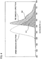
- red-green phosphorescent light-emitting layer 50 in the case where respective independent emission spectra of the red color phosphorescent material and the green color phosphorescent material are normalized, as shown in Fig. 4 , normalized spectra of these materials are overlapped.
- the area S1 of an overlap of the normalized spectrum of the red color phosphorescent material and the normalized spectrum of the green color phosphorescent material is less than or equal to 60% of the area S2 of the normalized spectrum of the red color phosphorescent material, and from the viewpoint of attaining higher color rendering properties, it is more preferred that the area S1 be less than or equal to 50% of the area S2.
- the area of an overlap of the emission spectrum of the red color phosphorescent material and the emission spectrum of the green color phosphorescent material is less than or equal to 60%, more preferably less than or equal to 50%, of the whole area of the emission spectrum of the red color phosphorescent material.
- the energy gap ⁇ E between the E LUMO and the E HOMO thereof be greater than or equal to 2.5 eV and less than or equal to 3.5 eV.
- the content of the red color phosphorescent material in the red-green phosphorescent light-emitting layer 50 is defined as X mass%, it is preferred that X be greater than or equal to 0.01 and less than 0.3. That is, it is preferred that the content of the red color phosphorescent material be greater than or equal to 0.01 mass% and less than 0.3 mass% in the red-green phosphorescent light-emitting layer 50.
- the content of the green color phosphorescent material in the red-green phosphorescent light-emitting layer 50 is defined as ( ⁇ ⁇ X) mass%, it is preferred that ⁇ be greater than or equal to 100 and less than 300. That is, it is preferred that the red-green phosphorescent light-emitting layer 50 include the green color phosphorescent material in an amount greater than or equal to 100 times and less than 300 times the amount of the red color phosphorescent material.
- the cathode electrode 6 is a cathode layer which has a conductivity, and functions as a cathode.
- the cathode electrode 6 is a conductive thin film layer producible from a conductive material easy to become a thin film-like shape.
- the cathode electrode 6 be a light reflecting thin film layer.
- the cathode electrode 6 can be formed of various metallic materials.
- the cathode electrode 6 reflect light emitted from the light-emitting layer 30 or 50 toward the translucent insulation substrate 1 side to enhance the light extraction efficiency, metals with a white luster are preferred, and of these, silver (Ag) and aluminum (Al) are more preferred.
- a light extraction layer 7 be provided at the outermost surface of a region at the light-emitting surface side including at least the light-emitting region 20.
- the light extraction layer 7 be provided at the light exiting side of a glass substrate.
- Examples of a method for forming the light extraction layer 7 include a nanoimprinting method of applying a resin composed of an acrylic resin and the like on the surface of a glass substrate as the translucent insulation substrate 1 and a method of subjecting a resin containing glass beads to spray-coating or slit-coating.
- a resin film (optical film) having one surface with a minute recess/protrusion structure and the other surface to which an adhesive material is stuck be attached to a surface at the light-emitting surface side of a glass substrate as the translucent insulation substrate 1 so as to make the one surface become the outermost surface mentioned above. That is, it is preferred that the light extraction layer 7 have minute recesses and protrusions formed on a surface at the opposite side to the translucent insulation substrate 1.
- Such an optical film constituting the light extraction layer 7 have light scattering properties.
- attaching an optical film constituting the light extraction layer 7 to the translucent insulation substrate 1 be performed after an organic EL element 10 is formed so as not to allow the film surface to suffer from scratches.
- the organic EL element 10 is provided with the layered structure of a translucent anode electrode 2/a hole injection layer/a hole transport layer/a blue light-emitting layer 30/an electron transport layer/a connection layer 4/a hole transport layer/a red-green phosphorescent light-emitting layer 50/an electron transport layer/an electron injection layer/a cathode electrode 6.
- the connection layer 4 includes an electron injecting surface layer arranged at the blue light-emitting layer 30 side and a hole injecting surface layer arranged at the red-green phosphorescent light-emitting layer 50 side.
- Examples of the hole injection layer include a layer taking in holes from the translucent anode electrode 2 (positive electrode) side and injecting holes into a hole transport layer.
- a arylamine a kind of phthalocyanine, oxides such as vanadium oxide, molybdenum oxide, ruthenium oxide, aluminum oxide and titanium oxide; amorphous carbon; conductive polymers such as polyaniline, polythiophene, polyphenylene vinylene, and a derivative thereof; and the like can be adopted.
- the material for the hole injection layer from the viewpoint of enhancing the transparency of the hole injection layer to enhance the luminance, a material prepared by doping an electron-accepting dopant into a hole transporting material can also be preferably adopted.
- the average thickness of the hole injection layer be greater than or equal to 0.1 nm and less than or equal to 20 nm.
- the hole transport layer is a layer restricting the movement of electrons to the positive electrode side while effectively transporting holes from a hole injection layer side to the light-emitting layer 30 or 50.
- a known hole transporting material can be used as the material for the hole transport layer.
- the average thickness of the hole transport layer be greater than or equal to 1 nm and less than or equal to 200 nm.
- Each light-emitting layer is a layer prepared by doping a luminescent material into a host material having a hole transporting property or an electron transporting property, and is a layer in which the hole flowing thereinto from a hole transport layer and the electron flowing thereinto from an electron transport layer are combined by the electric field application to generate a light-emitting exciton.
- each light-emitting layer be greater than or equal to 1 nm and less than or equal to 40 nm.
- the electron transport layer is a layer restricting the movement of electrons to the cathode electrode 6 (negative electrode) side while effectively transporting electrons from an electron injection layer side to the light-emitting layer 30 or 50.
- the material for the electron transport layer a known electron transporting material can be used, and it is preferred that the average thickness thereof be greater than or equal to 1 nm and less than or equal to 200 nm.
- Examples of the electron injection layer include a layer taking in electrons from the cathode electrode 6 (negative electrode) side and injecting electrons into an electron transport layer.
- lithium (Li) compounds of an alkali metal or an alkaline earth metal such as lithium fluoride (LiF), cesium fluoride (CsF) and calcium fluoride (CaF 2 ), and the like can be adopted.
- LiF lithium fluoride
- CsF cesium fluoride
- CaF 2 calcium fluoride
- the material for the electron injection layer from the viewpoint of enhancing the transparency of the electron injection layer to enhance the luminance, a material prepared by doping an electron-donating dopant into an electron transporting material can also be preferably adopted.
- the average thickness of the electron injection layer be greater than or equal to 0.1 nm and less than or equal to 20 nm.
- the hole transporting material for example, a triphenylamine-based compound, a carbazole-based compound, and the like can be adopted.
- triphenylamine-based compound examples include N,N'-bis(3-methylphenyl)-(1,1'-biphenyl)-4,4'-diamine (TPD), 4,4'-bis[N-(naphthyl)-N-phenyl-amino]biphenyl ( ⁇ ,-NPD), 4,4',4"-tris(N-(3-methylphenyl)N-phenylamino)triphenylamine (MTDATA), 4,4',4"-tris[N,N-(2-naphthyl)phenylamino]triphenylamine (2-TNATA), and the like.
- carbazole-based compound examples include 4,4'-N,N'-dicarbazole-biphenyl (CBP), 4,4',4"-tri(N-carbazolyl)triphenylamine (TCTA), 4,4'-N,N'-dicarbazole-2,2'-dimethylbiphenyl (CDBP), and the like.
- the electron transporting material for example, a quinolinolato-based metal complex, an anthracene-based compound, an oxadiazole-based compound, a triazole-based compound, a phenanthroline-based compound, a silole-based compound, and the like can be adopted.
- quinolinolato-based metal complex examples include tris(8-quinolinolato)aluminum (Alq3), bis(2-methyl-8-quinolinolato)(p-phenyl phenolato)aluminum (BAlq), and the like.
- anthracene-based compound examples include 3-t-butyl-9,10-di(2-naphthyl)anthracene (TBADN), 9,10-di(2-naphthyl)anthracene (ADN), and the like.
- oxadiazole-based compound examples include 1,3-bis[(4-t-butylphenyl)-1,3,4-oxadiazole]phenylene (OXD-7), 2-(4-biphenylyl)-5-(4-t-butylphenyl)-1, 3,4-oxadiazole (PBD), 1,3,5-tris(4-t-butylphenyl-1,3,4-oxadiazolyl)benzene (TPOB), and the like.
- OXD-7 1,3-bis[(4-t-butylphenyl)-1,3,4-oxadiazole]phenylene
- PBD 2-(4-biphenylyl)-5-(4-t-butylphenyl)-1, 3,4-oxadiazole
- TPOB 1,3,5-tris(4-t-butylphenyl-1,3,4-oxadiazolyl)benzene
- triazole-based compound examples include 3-phenyl-4-(1'-naphthyl)-5-phenyl-1,2,4-triazole (TAZ), and the like.
- phenanthroline-based compound examples include bathophenanthroline (Bphen), bathocuproine (BCP), and the like.
- silole-based compound examples include 2,5-di-(3-biphenyl)-1,1-dimethyl-3,4-diphenylsilacyclopentadiene (PPSPP), 1,2-bis(1-methyl-2,3,4,5-tetraphenylsilacyclopentadienyl)ethane (2PSP), 2,5-bis-(2,2-bipyridine-6-yl)-1,1-dimethyl-3,4-diphenylsilacyclopentadiene (PyPySPyPy), and the like.
- PPSPP 2,5-di-(3-biphenyl)-1,1-dimethyl-3,4-diphenylsilacyclopentadiene
- PPSPP 1,2-bis(1-methyl-2,3,4,5-tetraphenylsilacyclopentadienyl)ethanethanethanethanethanethanethanethanethanethanethanethanethanethane
- Luminescent materials constituting each light-emitting layer are classified into a fluorescent material and a phosphorescent material which is generally higher in luminous efficiency than the former.
- red color-based fluorescent light-emitting material rubrene, DCM, DCM2, DBzR, and the like can be adopted.
- coumarin 6, C545T, and the like can be adopted as a green color-based fluorescent light-emitting material.
- perylene 4,4'-bis(9-ethyl-3-carbazovinylene)-1,1-biphenyl BCzVBi
- 4,4'-bis[4-(di-p-triamino)styryl]biphenyl DPAVBi
- BCzVBi perylene 4,4'-bis(9-ethyl-3-carbazovinylene)-1,1-biphenyl
- DPAVBi 4,4'-bis[4-(di-p-triamino)styryl]biphenyl
- red color-based phosphorescent light-emitting material As a red color-based phosphorescent light-emitting material, (bzq)2Ir(acac), (btp)2Ir(acac), Ir(bzq)3, and Ir(piq)3 which are iridium complexes, and the like can be adopted.
- FIrpic, FIr6 and Ir(Fppy)3 which are iridium complexes, and the like can be adopted.
- a tetracyanoquinodimethane-based compound molybdenum oxide (MoO 3 ), tungsten oxide (WO 3 ), vanadium oxide (V 2 O 5 ), and the like can be adopted.
- MoO 3 molybdenum oxide
- WO 3 tungsten oxide
- V 2 O 5 vanadium oxide
- tetracyanoquinodimethane-based compound examples include tetracyanoquinodimethane (TCNQ), 2,3,5,6-tetrafluoro-7,7,8,8-tetracyanoquinodimethane (F4-TCNQ), and the like.
- an alkali metal, an alkaline earth metal, a rare earth metal, a compound of these metals, a phthalocyanine complex making any of these metals the central metal, a dihydroimidazole compound, and the like can be adopted.
- alkali metal examples include lithium (Li), sodium (Na), potassium (K), rubidium (Rb), cesium (Cs), and the like.
- alkaline earth metal examples include magnesium (Mg), calcium (Ca), strontium (Sr), barium (Ba), and the like.
- dihydroimidazole compound examples include bis-[1,3-diethyl-2-methyl-1,2-dihydrobenzimidazolyl]tetrathiafulvalene (TTF), tetrathianaphthacene (TTT), and the like.
- the cathode side red-green light-emitting unit 5 is provided with the red-green phosphorescent light-emitting layer 50 in which a red color phosphorescent material and a green color phosphorescent material are combined with a host material for the phosphorescent light-emitting layer, in the red-green phosphorescent light-emitting layer 50, the red shift attributed to the green color phosphorescent material can be made to stably occur. As such, the ratio of the green emission and the red emission can be kept constant regardless of the temperature of the organic EL element 10 and the current density, and a widely ranging emission spectrum from red color close to natural light can be obtained.
- the red-green phosphorescent light-emitting layer 50 is easily formed because the red-green phosphorescent light-emitting layer 50 in the cathode side red-green light-emitting unit 5 is formed by subjecting a host material for the phosphorescent light-emitting layer, a red color phosphorescent material and a green color phosphorescent material to co-vapor deposition.
- the white light-emitting organic EL panel 100 is a bottom emission type organic EL panel in which white light is taken out from the translucent insulation substrate 1 side, but the present invention is not limited thereto.
- the white light-emitting organic EL panel may be a top emission type organic EL panel in which white light is taken out from the opposite side to the substrate.
- a resultant light composed of two kinds of light emitted from two light-emitting units of the anode side blue light-emitting unit 3 and the cathode side red-green light-emitting unit 5 is used to generate white light, but the present invention is not limited thereto.
- a resultant light composed of three or more kinds of light emitted from three or more light-emitting units may be used to generate white light.
- each of the light-emitting units 3, 5 is provided with a hole injection layer, an electron injection layer and the like, but the present invention is not limited thereto.
- Each of the light-emitting units 3, 5 needs only to be provided with at least a light-emitting layer.
- an organic EL element 10 may have a layered structure with a stack of a translucent anode electrode 2/a hole transport layer/a blue light-emitting layer 30/an electron transport layer/a connection layer 4/a hole transport layer/a red-green phosphorescent light-emitting layer 50/an electron transport layer/an electron injection layer/a cathode electrode 6.
- Example 1 a white light-emitting organic EL panel 100 shown in Fig. 1 and Fig. 2 was prepared.
- a substrate in which an ITO layer with a thickness of 120 nm was formed on a glass substrate with outline dimensions of 80 mm ⁇ 80 mm and a thickness of 0.7 mm was prepared.
- a multilayer film 11 was formed according to the following procedure to form an organic EL element 10 having a light-emitting region 20 of 70.2 mm ⁇ 70.2 mm.
- a sealing film 12 was formed so that the light-emitting region 20 is contained therein when planarly viewed to form a sealed region 70.
- an optical film (OCF film) as a light extraction layer 7 was attached to the front surface side of the substrate to prepare a white light-emitting organic EL panel 100.
- an ITO layer was firstly formed on a glass substrate, the ITO layer on the glass substrate was patterned by a wet etching method to form a translucent anode electrode 2 and other portions, and a substrate for forming an organic EL element was prepared.
- FIG. 5 is a sectional configuration diagram of the organic EL element 10 of Example 1.
- a vacuum vapor deposition was performed at a deposition rate of about 0.1 nm/sec under vacuum at a degree of vacuum of 1 ⁇ 10 -4 Pa or more so that the film thickness-configuration of the respective layers shown in Fig. 5 is attained.
- the materials were subjected to co-vapor deposition at a prescribed mixing ratio.
- a cathode electrode 6 as a cathode was deposited at a rate of 0.1 to 0.3 nm/sec under vacuum.
- a silicon nitride film with an average thickness of 2 ⁇ m was formed by a CVD method using a prescribed mask, subsequently, polysilazane was applied thereon by a spraying method, and the film was fired to form a silica conversion layer (a silica layer obtained through conversion) as an inorganic sealing layer with an average thickness of 2 ⁇ m. Furthermore, onto the organic EL element 10 sealed with this inorganic sealing layer, a protective film composed of PET (Poly(ethylene terephthalate)) with an adhesive material was attached to form a sealed region 70.
- PET Poly(ethylene terephthalate
- an optical film (OCF film) was attached to a surface at the opposite side to the surface of the glass substrate on which the organic EL element 10 was formed to prepare a white light-emitting organic EL panel 100 of Example 1.
- the average thickness of a fluorescent blue light-emitting layer which is a blue light-emitting layer 30 was determined to be 22 nm and the average thickness of a phosphorescent red-green light-emitting layer which is a red-green phosphorescent light-emitting layer 50 was determined to be 26 nm.
- a red color phosphorescent material a green color phosphorescent material and a host material for the phosphorescent light-emitting layer, which constitute a phosphorescent red-green light-emitting layer, the following materials were used, respectively.
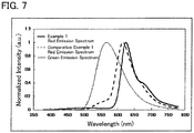
- red color phosphorescent material a material making the red emission spectrum thereof have a maximum emission peak wavelength of 625 nm was adopted.
- green color phosphorescent material a material making the green emission spectrum thereof have a maximum emission peak wavelength of 560 nm was adopted.
- host material for the phosphorescent light-emitting layer a material having an energy gap ⁇ E between the E LUMO and the E HOMO of 3.1 eV was adopted.
- the content of the red color phosphorescent material in the red-green phosphorescent light-emitting layer 50 was set to 0.25 mass% and the content of the green color phosphorescent material in the red-green phosphorescent light-emitting layer 50 was set to 20 mass%.
- the area of an overlap of the red emission spectrum of the red color phosphorescent material and the green emission spectrum of the green color phosphorescent material was determined to be 51 % of the area of the red emission spectrum.
- a blue color fluorescent material constituting a fluorescent blue light-emitting layer a material making the blue emission spectrum thereof have a maximum emission peak wavelength of 465 nm and making the monochromatic light normalized spectrum thereof have a half-value width of 60 nm was adopted.
- a constant current of 4 mA/cm 2 was made to pass through the white light-emitting organic EL panel 100 thus obtained and the emitted light from the light-emitting region 20 was measured using a spectroradiometer CS-1000 (available from KONICA MINOLTA SENSING AMERICAS, INC.) to evaluate the chromaticity, the color rendering index and the emission spectrum.
- the white color emission spectrum is shown in Fig. 6 .
- the emitted light of the white light-emitting organic EL panel 100 was determined to have a color temperature of 4000 K, a luminance value of 3000 cd/m 2 , an Ra value for color rendering properties of 92 and an R9 value therefor of 97. Moreover, with regard to the emitted light of the white light-emitting organic EL panel 100, the coordinate position in the CIE 1931 chromaticity coordinate system was determined to be at a distance of 0.004 from a black-body radiation curve.
- a rated luminance value of 3000 cd/m 2 was attained in the case where the rated current was set to 200 mA and a rated luminance value of 300 cd/m 2 was attained while maintaining a color temperature of 4000 K, which is equal to the color temperature thereof, in the case where the rated current was set to 20 mA. That is, in both cases where the rated current was set to 200 mA or 20 mA, basic hue values were determined to be the same as each other. It is thought that this is attributed to the high stability according to the present invention.
- a panel of Comparative Example 1 was prepared to be evaluated in the same manner as that in Example 1 except that a material having a maximum emission peak wavelength of 610 nm was adopted as the red color phosphorescent material.
- Example 1 the maximum emission peak wavelength of the red color phosphorescent material and the maximum emission peak wavelength of the green color phosphorescent material are apart from each other by 65 nm, and in contrast, in Comparative Example 1, the distance therebetween is 50 nm.
- a panel of Comparative Example 2 was prepared/evaluated in the same manner as that in Comparative Example 1 except that a material having a maximum emission peak wavelength of 451 nm was adopted as the blue color fluorescent material.
- Example 1 and Comparative Examples 1, 2 The chromaticity of each panel of Example 1 and Comparative Examples 1, 2, the general color rendering index Ra, the special color rendering index R9, the distance duv from a black-body radiation curve, and the red monochromatic emission spectrum/green monochromatic emission spectrum area ratio of luminescent materials of the red-green phosphorescent light-emitting layer 50 used in Example 1 and Comparative Example 1 are shown in Table 1.
- the general color rendering index Ra the special color rendering index R9, the deviation duv from a black-body locus, and the area ratio of the area of an overlap of the red emission spectrum of the red color phosphorescent material and the green emission spectrum of the green color phosphorescent material to the area of the red emission spectrum are shown in Table 1.
- a panel of Example 2 was prepared to be evaluated in the same manner as that in Example 1 except that film sealing by forming a sealing film by CVD method-film forming and the like was not performed and glass-made can sealing was performed.
- the panel of Example 2 thus prepared was determined to be a panel capable of setting the rated luminance value to 300 cd/m 2 and setting the rated color temperature to 4000 K in the case of making a current of 20 mA as the rated current flow therethrough.
- the basic hue was determined to be white color, and this is the same as the case of 20 mA.
- the color temperature was changed from 4000 K by an amount of change in temperature greater than 500 K, and it was difficult for the rated luminance value of the panel at a color temperature equal thereto to be attained.
- the hue of a product mentioned above is further stabilized, and even in the case where the rated current is changed from a smaller rated current to a larger rated current, it has been possible to set the rated luminance value while maintaining a color temperature equal thereto.
Landscapes
- Physics & Mathematics (AREA)
- Optics & Photonics (AREA)
- Chemical & Material Sciences (AREA)
- Engineering & Computer Science (AREA)
- Materials Engineering (AREA)
- Organic Chemistry (AREA)
- Manufacturing & Machinery (AREA)
- Electroluminescent Light Sources (AREA)
Abstract
Description
- The present invention relates to a white light-emitting organic EL panel and a production method thereof. In particular, the present invention relates to a white light-emitting organic EL panel which is capable of illuminating an object to be illuminated so as to reproduce a natural hue thereof and is excellent in color rendering properties, and a production method therefor.
- An organic EL element is a semiconductor element that converts electric energy into light energy.
- In recent years, researches on an organic EL element which is attempted to be applied particularly to a display screen of a mobile phone or a portable display device have been actively conducted. Moreover, improvements have been made to organic materials constituting the organic EL element and the like, and as a result, the drive voltage of the organic EL element has been remarkably lowered and the luminous efficiency has been heightened. From this, an organic EL panel in which an organic EL element highly increased in luminance and highly enhanced in efficiency is adopted as an illumination panel has been put into practical use and has begun to be sold in the market.
- In the case of using an organic EL panel as an illumination device, the organic EL panel is required to have high luminance and high luminous efficiency. In order to attain high luminance, it is necessary to make the applied current large and to make the current density per light-emitting area large. However, although the current density per light-emitting area applied to an organic EL panel can be made large to attain high luminance, in contrast thereto, there is a problem that a load is applied to an organic EL element built in the organic EL panel and the life of the organic EL element is liable to be shortened. On that account, Non-Patent
Document 1 discloses a lamination type organic EL element including a charge generating layer as an improvement method therefor. - Incidentally, in recent years, with regard to a next-generation illumination panel, the technological development of a method for imparting a panel with high color rendering properties at various color temperatures has been actively conducted.
- However, in the current situation of the white light-emitting organic EL panel, sufficiently high color rendering properties have not yet been realized as compared with a conventional fluorescent light. Particularly, in the case where an organic EL panel is made to have a luminance adjusting function and the current density is changed to make the organic EL panel variable in luminance, the color temperature is difficult to be maintained constant due to a change in current density at the time of changing the luminance. As such, in order to realize a white light-emitting organic EL panel having both high stability and high color rendering properties, some challenges still remain to be done.
- In this context, with regard to a white light source with three primary colors of red/green/blue, it is advantageous for an increase in luminance and an enhancement in efficiency to heighten the emission intensity of green color with a large luminosity factor. As such, in a conventional panel, it is common for the maximum emission position (hereinafter, also referred to as peak wavelength) of the emission spectrum of green color and the peak wavelength of the emission spectrum of red color to be closely arranged so that the emission spectra of green color and red color are overlapped.
- However, in such a structure, the luminance can be enhanced, but the general color rendering index Ra is not more than 80 or so and there has been a limit to the reproducibility of a natural hue of an object to be illuminated. Particularly, in the conventional panel, there has been a problem that the special color rendering index R9 remains 20 to 30 or so and red color fails to be vividly reproduced.
- Moreover, when the peak wavelength of a green color phosphorescent light-emitting layer is arranged close to the peak wavelength of a red color phosphorescent light-emitting layer, the emission spectrum of the green color phosphorescent light-emitting layer is made to shift to the red side and reddish green color is emitted from the green color phosphorescent light-emitting layer. That is, when the red shift occurs at the green color phosphorescent light-emitting layer, it is disadvantageous for an enhancement in efficiency and there is also a problem that the phosphorescence luminescent material, which is relatively expensive, is wastefully consumed.
- On that account, in
Patent Document 1, there has been proposed an organic electroluminescent element having two maximum emission wavelengths in the emission spectrum of blue color ranging from 440 to 490 nm, one maximum emission wavelength in the emission spectrum of green color ranging from 500 to 540 nm and one maximum emission wavelength in the emission spectrum of red color ranging from 600 to 640 nm, wherein the maximum emission wavelength of green color and the maximum emission wavelength of blue color are arranged so as to have a certain distance or more therebetween and the maximum emission wavelength of green color and the maximum emission wavelength of red color are arranged so as to have a predetermined distance or more therebetween. According to the element of thePatent Document 1, without making the red shift occur, the general color rendering index Ra higher than that of the conventional panel is attained. - Patent Document 1:
JP 2014-011208 A - Non-Patent Document 1: Appl. Phys. Lett. Vol. 80, p1667 (2002)
- In the element of the
Patent Document 1, since a red color phosphorescent light-emitting layer is provided adjacent to a green color phosphorescent light-emitting layer without a connection layer interposed therebetween, the position of the emission interface as the reaction field in the green color phosphorescent light-emitting layer and the red color phosphorescent light-emitting layer depends on the moving speed of electrons and holes. As such, when the current density is changed, the moving speed of electrons and holes is changed and the position of the emission interface where electrons and holes react with each other varies and is not stabilized. Therefore, in the element described inPatent Document 1, with regard to the color temperature and color rendering properties, the temperature dependency and the current density dependency become large and there is a problem that the hue of a product is not stabilized. Particularly, in the case where the element described inPatent Document 1 is made variable in luminance at a prescribed color temperature, since the temperature generated during the light emission and the density of a current vary with the luminance, there is also a problem that the performance guarantee range therefor is difficult to be sufficiently widely secured. - On that account, the present invention aims at providing a white light-emitting organic EL panel which is high in color rendering properties and is excellent in hue stability of a basic product prepared therewith and a production method therefor.
- In view of such problems, the present inventors thought that a red color phosphorescent material constituting a red phosphorescent light-emitting layer and a green color phosphorescent material constituting a green phosphorescent light-emitting layer are subjected to co-vapor deposition to prepare a composite layer so that red light and green light in specific proportions are emitted even in the case where the emission interface is arranged in any position, and a green color phosphorescent light-emitting material can be made to shift to the red side intentionally. Since the green color phosphorescent material is thus made to shift to the red side stably and the emission color is stabilized because the ratio of the red emission and the green emission becomes constant even when the emission interface as the reaction field is arranged in any position, the present inventors have found that the color rendering properties and the stability of a basic product hue can be secured.
- According to an aspect of the present invention derived from such findings, there is provided a white light-emitting organic EL panel including an organic EL element that includes: an anode layer; a cathode layer; and a light-emitting functional layer between the anode layer and the cathode layer, the light-emitting functional layer including in order from the anode layer toward the cathode layer: an anode side blue light-emitting unit; a connection layer; and a cathode side red-green (red and green) light-emitting unit, the connection layer injecting electrons into the anode side blue light-emitting unit and injecting holes into the cathode side red-green light-emitting unit when current is applied, the cathode side red-green light-emitting unit including a red-green phosphorescent light-emitting layer that is a composite layer including: a red color phosphorescent material; a green color phosphorescent material; and a host material for the phosphorescent light-emitting layer, wherein maximum emission peak wavelength of the red color phosphorescent material is apart from maximum emission peak wavelength of the green color phosphorescent material by 60 nm or more, and wherein the white light-emitting organic EL panel is capable of emitting white light with an general color rendering index Ra and a special color rendering index R9 in accordance with JIS Z 8726, both of the Ra and the R9 being greater than or equal to 90.
- This so-called "red color phosphorescent material" refers to a luminescent material exhibiting red color phosphorescent light emission.
- This so-called "green color phosphorescent material" refers to a luminescent material exhibiting green color phosphorescent light emission.
- According to this aspect, since the cathode side red-green light-emitting unit is provided with a red-green phosphorescent light-emitting layer as a composite layer in which a red color phosphorescent material and a green color phosphorescent material are combined with a host material for the phosphorescent light-emitting layer, in the red-green phosphorescent light-emitting layer, the red shift attributed to the green color phosphorescent material can be made to stably occur. As such, the ratio of the green emission and the red emission is kept constant independently of the temperature of the organic EL element and the current density, and a widely ranging emission spectrum from deep crimson can be obtained. Therefore, the panel is high in color rendering properties and is excellent in stability of color temperature and stability of basic color rendering properties.
- In a preferred aspect thereof, the organic EL element is laminated on a substrate, and the white light-emitting organic EL panel further includes a sealing film that seals the organic EL element between the sealing film and the substrate, the sealing film including an inorganic sealing layer in contact with the organic EL element.
- According to this aspect, since the stability effect is sufficiently exerted and the panel is usable in a wide luminance range, the panel can realize high reliability, thus hardly causing a problem such as the occurrence of lighting failure.
- In a preferred aspect thereof, the white light has a rated color temperature within a range of 500 K or lower, and at the rated color temperature, the white light-emitting organic EL panel is capable of being set to at least a first rated luminance value and a second rated luminance value, the two rated luminance values being allocated so as to have 2000 cd/m2 in between, the second rated luminance value being greater than or equal to 2 times of the first rated luminance value.
- According to this aspect, since the panel is made to have a plurality of rated luminance values at a rated color temperature, the brightness is easily adjusted. Moreover, according to this aspect, even in such a case of being variable in luminance, it is possible to secure a sufficiently wide performance guarantee range therefor.
- In a preferred aspect thereof, the host material for the phosphorescent light-emitting layer has an energy gap ΔE between ELUMO and EHOMO greater than or equal to 2.5 eV and less than or equal to 3.5 eV.
- According to this aspect, the panel is further increased in stability of the red shift attributed to the green color phosphorescent material. Based on the green phosphorescence excellent in such a basic stability, the possibility that red phosphorescence is caused only by the red shift is heightened. With this setup, since the stability of the ratio of the green emission and the red emission is further enhanced, the panel becomes smaller in temperature dependency and current density dependency. That is, according to this aspect, red phosphorescence can be made to stably occur by virtue of the green color phosphorescent material, and this enables the luminescent color to be hardly affected by the temperature and the like.
- In a preferred aspect thereof, the red-green phosphorescent light-emitting layer includes: the red color phosphorescent material in an amount greater than or equal to 0.01 mass% and less than or equal to 0.3 mass%; and the green color phosphorescent material in an amount greater than or equal to 100 times and less than 300 times of the red color phosphorescent material.
- That is, when the content of the red color phosphorescent material in the red-green phosphorescent light-emitting layer is defined as X mass% and the content of the green color phosphorescent material therein is defined as α × X mass%, it is preferred that X be greater than or equal to 0.01 and less than 0.3 and α be greater than or equal to 100 and less than 300.
- According to these aspects, the content of the red color phosphorescent material in the red-green phosphorescent light-emitting layer is small, and the content of the green color phosphorescent material in the red-green phosphorescent light-emitting layer is significantly larger than the content of the red color phosphorescent material. As such, the occurrence degree of red phosphorescence by only the red shift attributed to green phosphorescence is further heightened. Therefore, the panel can be made to become smaller in temperature dependency and current density dependency.
- In a preferred aspect thereof, an emission spectrum of the white light has an emission peak within the range of 500 nm to 580 nm and another emission peak within the range of 590 nm to 630 nm.
- According to this aspect, by a relatively simple configuration, white light with an general color rendering index Ra value and a special color rendering index R9 value serving as indexes of color rendering properties, both of which are greater than or equal to 90, is easily obtained. Moreover, according to this aspect, red phosphorescence by substantially only the red shift of the green color phosphorescent material is made to easily occur. That is, according to this aspect, based on an increase in red monochromatic light-emission by red shift, the stability of a product hue can be further enhanced.
- In a preferred aspect thereof, a coordinate position of the white light in CIE 1931 chromaticity coordinate system is at a distance less than or equal to 0.005 from a black-body radiation curve.
- According to this aspect, the reproducibility of a natural hue of an object to be illuminated can be further enhanced. That is, according to this aspect, the panel is made to have more enhanced hue reproducibility.
- In a preferred aspect thereof, the color temperature of the white light is higher than or equal to 3000 K and lower than or equal to 5000 K, and the white light has an emission peak within a range of 455 nm or more and 470 nm or less as its spectrum, the emission peak having a half-value width greater than or equal to 50 nm.
- According to this aspect, with regard to the blue emission, the panel is made to have a more enhanced reproducibility of a natural hue of an object to be illuminated.
- In a preferred aspect thereof, an area on which the red emission spectrum of the red color phosphorescent material and the green emission spectrum of the green color phosphorescent material overlap is less than or equal to 60% of an area of the red emission spectrum.
- According to this aspect, the panel is made to become high in red monochromatic light-emission by red shift and can be made to have a more enhanced reproducibility of a natural hue of an object to be illuminated.
- In a preferred aspect thereof, the organic EL element is laminated on a translucent insulation substrate, and the panel is capable of emitting the white light from a side of the translucent insulation substrate.
- There is provided a production method for a white light-emitting organic EL panel in the above-mentioned aspect, including the step of comprising the step of performing co-vapor deposition of the red color phosphorescent material, the green color phosphorescent material, and the host material for the phosphorescent light-emitting layer to form the red-green phosphorescent light-emitting layer.
- According to this aspect, the red-green phosphorescent light-emitting layer can be formed by one process and is easily produced.
- According to the present invention, the panel is made to become high in both the general color rendering index Ra and the special color rendering index R9 for red color and is made to become excellent in the stability of color temperature and color rendering properties.
-
-
Fig. 1 is a perspective view showing a white light-emittingorganic EL panel 100 in accordance with one embodiment of the present invention. -
Fig. 2 is a schematic sectional view showing anorganic EL element 10 in accordance with one embodiment of the present invention. -
Fig. 3 is an explanatory diagram showing an emission spectrum of white light emitted from a white light-emittingorganic EL panel 100 of the present invention. -
Fig. 4 is an explanatory diagram prepared by normalized emission spectra of light emitted only from a red color phosphorescent material and light emitted only from a green color phosphorescent material. -
Fig. 5 is a sectional configuration diagram of anorganic EL element 10 of Example 1. -
Fig. 6 shows an emission spectrum of a white light-emitting organic EL panel of Example 1. -
Fig. 7 shows normalized emission spectra which are obtained under the same current density and respectively represent the monochromatic structure of each of a red color phosphorescent material used in Example 1 or a red color phosphorescent material used in Comparative Example 1 and a green color phosphorescent material used together with these respective materials. - Hereinafter, a embodiment according to the present invention will be described in detail.
- Hereinafter, a white light-emitting
organic EL panel 100 of the present invention will be described with reference toFig. 1 . That is,Fig. 1 is a perspective view showing the white light-emittingorganic EL panel 100 in accordance with one embodiment of the present invention. - The white light-emitting
organic EL panel 100 has a light-emitting surface and a rear surface as both main surfaces. The white light-emittingorganic EL panel 100 has a built-inorganic EL element 10 and emits white light from a light-emittingregion 20 at the light-emitting surface side based on the light emission of theorganic EL element 10. The white light-emittingorganic EL panel 100 is a member in a planarly spread state, and specifically, is a plate-like panel. - First, prior to the description for the respective constituent elements constituting the white light-emitting
organic EL panel 100, physical properties of white light capable of being emitted from the white light-emittingorganic EL panel 100 will be described. In this connection, in the case where the panel of the present invention is provided with alight extraction layer 7 described below like the white light-emittingorganic EL panel 100 in accordance with the present embodiment, measured values are values obtained when white light transmitted through thelight extraction layer 7 is measured for the color rendering properties, the spectrum, and the color temperature. - The white light-emitting
organic EL panel 100 emits specific white light attributed to theorganic EL element 10 from the light-emitting surface. Both of the general color rendering index Ra and the special color rendering index R9 of white light emitted from this white light-emittingorganic EL panel 100 in accordance with JIS Z 8726 are greater than or equal to 90. - Moreover, with regard to the white light-emitting
organic EL panel 100, the amount of change in the color temperature or the color rendering properties with a change in the current density or the element temperature of theorganic EL element 10 caused mainly by the change of luminance is small, and the panel has a stability. - It is preferred that the white light-emitting
organic EL panel 100 be made to have a plurality of rated luminance values having a rated color temperature within a prescribed color temperature range. That is, it is preferred that the white light-emittingorganic EL panel 100 be used as an illumination panel variable in luminance. The rated luminance of the white light-emittingorganic EL panel 100 of the present embodiment is capable of being set to a value among two or more rated luminance values L1, L2 and the like at a rated color temperature within a prescribed color temperature range by changing the current density and the like. - In the case where, like the white light-emitting
organic EL panel 100 of the present embodiment, a rated color temperature within a prescribed color temperature range is secured and at least two rated luminance values L1, L2 and the like, which are different from one another in luminance, exist, it is preferred that one rated luminance value L1 be greater than or equal to 2000 cd/m2 and the other rated luminance value L2 be less than or equal to 2000 cd/m2. Furthermore, it is preferred that these two rated luminance values L1 and L2 be two values, between which a value of 2000 cd/m2 is interposed, of a smaller value and a larger value having an intensity greater than or equal to 2 times the intensity of the smaller value as the difference. That is, it is preferred that the rated luminance values L1 and L2 satisfy the relationship of (L1 - L2) ≥ L2 × 2. - With regard to the two rated luminance values L1 and L2, it is preferred that a rated color temperature within the color temperature range of 500 K or lower be secured, and it is more preferred that a rated color temperature within the color temperature range of 200 K or lower be secured.
- With regard to the luminance range within which the two rated luminance values L1 and L2 are included, the range of 0.5 cd/m2 to 20000 cd/m2 is preferred, the range of 1 cd/m2 to 10000 cd/m2 is more preferred and the range of 10 cd/m2 to 5000 cd/m2 is further preferred.
- The rated color temperature is higher than or equal to 1000 K and lower than or equal to 10000 K and is preferably higher than or equal to 3000 K and lower than or equal to 6000 K. As mentioned above, the white light-emitting
organic EL panel 100 of the present embodiment has two or more rated luminance values L1, L2 and the like. And then, with regard to the white light-emittingorganic EL panel 100 of the present embodiment, among these two rated luminance values L1 and L2, one rated luminance value L1 is greater than or equal to 2000 cd/m2 and less than or equal to 20000 cd/m2 and the other rated luminance value L2 is greater than or equal to 0.5 cd/m2 and less than 2000 cd/m2. - With regard to white light emitted from the white light-emitting
organic EL panel 100, as shown inFig. 3 , the emission spectrum thereof has at least two emission peaks, and it is preferred that the emission spectrum thereof have a first emission peak within a wavelength range (first wavelength range) of 500 nm or more and 580 nm or less and a second emission peak within a wavelength range (second wavelength range) of 590 nm or more and 630 nm or less. - With regard to white light emitted from the white light-emitting
organic EL panel 100, furthermore, it is more preferred that the emission spectrum thereof have a third emission peak within a wavelength range (third wavelength range) of 455 nm or more and 470 nm or less, and it is further preferred that the half-value width of the third emission peak be greater than or equal to 50 nm. - With regard to emitted light from the white light-emitting
organic EL panel 100 of the present embodiment, as shown inFig. 3 , the emission spectrum thereof has three emission peaks, and three peak wavelengths corresponding to the emission peaks lie within a wavelength range of 455 nm or more and 470 nm or less, a wavelength range of 500 nm or more and 580 nm or less and a wavelength range of 590 nm or more and 630 nm or less, respectively. - Moreover, with regard to white light emitted from the white light-emitting
organic EL panel 100, it is preferred that the coordinate position in the CIE 1931 chromaticity coordinate system be at a distance less than or equal to 0.005 from a black-body radiation curve. That is, with regard to white light emitted from the white light-emittingorganic EL panel 100, it is preferred that the deviation duv from a black-body locus be less than or equal to 0.005. - With regard to white light emitted from the white light-emitting
organic EL panel 100, it is preferred that the color temperature thereof be higher than or equal to 3000 K and lower than or equal to 5000 K, and it is further preferred that the color temperature thereof be higher than or equal to 4000 K. - Subsequently, the respective constituent elements of the white light-emitting
organic EL panel 100 in accordance with one embodiment of the present invention will be described. - The white light-emitting
organic EL panel 100 is a so-called bottom emission type organic EL panel. - The white light-emitting
organic EL panel 100 is prepared by laminating amultilayer film 11 in which anorganic EL element 10 is included as a component thereof on atranslucent insulation substrate 1, and theorganic EL element 10 is sealed with a sealingfilm 12. - The
multilayer film 11 includes a translucent anode electrode 2 (anode layer), an anode side blue light-emitting unit 3, aconnection layer 4, a cathode side red-green light-emittingunit 5 and a cathode electrode 6 (cathode layer) which are arranged in this order from thetranslucent insulation substrate 1 side. Theorganic EL element 10 is a portion composed of thetranslucent anode electrode 2, the anode side blue light-emitting unit 3, theconnection layer 4, the cathode side red-green light-emittingunit 5, and thecathode electrode 6, which are superimposed when planarly viewed. Considering from a different point of view, theorganic EL element 10 is prepared by sandwiching a light-emittingfunctional layer 8 between thetranslucent anode electrode 2 and thecathode electrode 6, and the light-emittingfunctional layer 8 is a laminate composed of the anode side blue light-emitting unit 3, theconnection layer 4, and the cathode side red-green light-emittingunit 5. - The
organic EL element 10 belongs to a light-emittingregion 20 and coincides with the light-emittingregion 20 when planarly viewed. - The white light-emitting
organic EL panel 100 has a light-emittingregion 20 on the light-emitting surface thereof corresponding to theorganic EL element 10. - Like the white light-emitting
organic EL panel 100 in accordance with the present embodiment, in the case where a panel has a plurality of rated luminance values L1, L2 and the like at one rated color temperature, it is preferred that the panel be provided with a sealedregion 70 covering the light-emittingregion 20 when planarly viewed at the rear surface side thereof. That is, it is preferred that the white light-emittingorganic EL panel 100 be provided with a sealedregion 70 overlapped with the light-emittingregion 20 when planarly viewed. - Thus, the occurrence of the dark spot (hereinafter, also referred to as DS) associated with a temperature rise of the
organic EL element 10 at the time of being used at high luminance and the shortening of the life thereof can be prevented. - The sealing
film 12 is a sealing layer forming the sealedregion 70 and includes an inorganic sealing layer brought into contact with theorganic EL element 10. - It is preferred that the average thickness of the sealing
film 12 be greater than or equal to 1 µm and less than or equal to 10 µm. - Thus, the panel can be prevented from suddenly suffering from lighting failure while being used to emit light.
- It is preferred that the sealing
film 12 include the inorganic sealing layer and an adhesive layer brought into contact with the inorganic sealing layer. It is more preferred that the sealingfilm 12 further have a heat equalizing film, an outer packaging film and the like on the adhesive layer. - As described above, by adopting the sealing structure by means of a film instead of the sealing structure by means of a glass-made can as its sealing structure, the sealing performance is heightened, and the stability effect attained by making the green color phosphorescent material shift to the red side can be sufficiently exerted.
- The
organic EL element 10 has a layered structure constituted of atranslucent anode electrode 2, an anode side blue light-emitting unit 3, aconnection layer 4, a cathode side red-green light-emittingunit 5, and acathode electrode 6, which are layered in this order from thetranslucent insulation substrate 1 side. That is, theorganic EL element 10 is provided with a light-emittingfunctional layer 8 constituted of the anode side blue light-emitting unit 3, theconnection layer 4 and the cathode side red-green light-emittingunit 5 between thetranslucent anode electrode 2 and thecathode electrode 6. - Each of the anode side blue light-emitting unit 3 and the cathode side red-green light-emitting
unit 5 is a light-emitting unit. - The anode side blue light-emitting unit 3 is positioned at the more
translucent anode electrode 2 side than theconnection layer 4 when cross-sectionally viewed. - The anode side blue light-emitting unit 3 may be a unit which emits light of any color other than blue as a whole as long as the unit has a light-emitting layer emitting light of blue color.
- The cathode side red-green light-emitting
unit 5 is positioned at themore cathode electrode 6 side than theconnection layer 4 when cross-sectionally viewed. - As long as the cathode side red-green light-emitting
unit 5 has a red-green phosphorescent light-emittinglayer 50 emitting phosphorescent light of red color and phosphorescent light of green color, the cathode side red-green light-emittingunit 5 may have an additional light-emitting layer, but it is preferred that the cathode side red-green light-emittingunit 5 have only the red-green phosphorescent light-emittinglayer 50 as the light-emitting layer. - Moreover, as long as the
organic EL element 10 includes the anode side blue light-emitting unit 3 and the cathode side red-green light-emittingunit 5, theorganic EL element 10 can include an additional light-emitting unit together with an additional connection layer other than theconnection layer 4. That is, as long as theorganic EL element 10 has the layered structure prepared by sandwiching theconnection layer 4 between the anode side blue light-emitting unit 3 and the cathode side red-green light-emittingunit 5, theorganic EL element 10 may be provided with an additional light-emitting unit and an additional connection layer. - A light-emitting unit is constituted of a plurality of layers composed mainly of an organic compound. As such an organic compound, known compounds such as a low-molecular coloring material and a conjugated polymer material which are generally used for an organic EL element can be used.
- Moreover, as long as the light-emitting unit described above has a light-emitting layer that emits light actually in the layer itself, the light-emitting unit can include a plurality of layers such as a hole injection layer, a hole transport layer, an electron transport layer, and an electron injection layer other than the light-emitting layer. These layers other than the light-emitting layer have a function of promoting the light emission mainly in the light-emitting layer.
- In this context, the hole injection layer and the electron injection layer can be substituted with a hole injecting surface layer or an electron injecting surface layer of a connection layer described below, respectively.
- Moreover, these layers can be formed appropriately by a known method such as a vacuum vapor deposition method, a sputtering method, a CVD method, a dipping method, a roll coating method (printing method), a spin coating method, a bar coating method, a spraying method, a die coating method and a flow coating method. From the viewpoint of preparing a high-performance element, it is preferred that these layers be formed by a vacuum vapor deposition method.
- The
translucent insulation substrate 1 is a member which is in a planarly spread state and is composed of a translucent insulation material. - As the
translucent insulation substrate 1, a glass substrate, a resin film substrate or the like can be used. As thetranslucent insulation substrate 1, from the viewpoint of suppressing the intrusion of moisture into theorganic EL element 10, causing the lowering in performance, a glass substrate is preferred. Moreover, as thetranslucent insulation substrate 1, a flexible substrate can also be adopted. - The
translucent anode electrode 2 is an anode layer which has a translucency and a conductivity, and functions as an anode. - As the material for the
translucent anode electrode 2, transparent conductive metal oxides such as indium tin oxide (ITO), indium zinc oxide (IZO), stannic oxide (SnO2) and zinc oxide (ZnO) can be adopted, and from the viewpoint of preparing a high-performance element, ITO or IZO which has high transparency is preferred. - The anode side blue light-emitting unit 3 has a blue light-emitting
layer 30 emitting light of at least blue color. It is preferred that the anode side blue light-emitting unit 3 include a hole injection layer, a hole transport layer, a blue light-emittinglayer 30, an electron transport layer, and an electron injection layer, which are arranged in this order from thetranslucent anode electrode 2 side. - From the viewpoint of being made to have a prolonged life as compared with the case of using a blue color phosphorescent material, it is preferred that the blue light-emitting
layer 30 be a blue fluorescent light-emitting layer including a blue color fluorescent material. - It is preferred that the blue light-emitting
layer 30 have an emission peak within the range of 470 nm or less, it is more preferred that the blue light-emittinglayer 30 have an emission peak within the range of 455 nm or more and 470 nm or less, and it is further preferred that the blue light-emittinglayer 30 have an emission peak with a half-value width of 50 nm or more. - With regard to the blue light-emitting
layer 30 in the present embodiment, the peak wavelength is greater than or equal to 455 nm and less than or equal to 470 nm, and the blue light-emittinglayer 30 has an emission peak with a half-value width of 50 nm or more. In short, the blue light-emittinglayer 30 in the present embodiment mainly has an emission peak corresponding to the third emission peak of the white light mentioned above. - The
connection layer 4 is a layer having a function of injecting electrons into the anode side blue light-emitting unit 3 side and injecting holes into the cathode side red-green light-emittingunit 5 side when current is applied to theorganic EL element 10. As long as theconnection layer 4 has such a function, various kinds of materials such as organic materials can be used for theconnection layer 4. Moreover, various kinds of materials can also be used in combination. - With regard to the
connection layer 4, from the viewpoint of enhancing the transparency thereof to attain the enhancement in luminance and the viewpoint of enhancing the injecting performance thereof for the respective electric charges to attain the enhancement in electrical properties, it is preferred that injection layers for the respective electric charges be used in combination. - It is more preferred that the
connection layer 4 be a layer prepared by doping an electron-accepting or electron-donating dopant into each of transporting materials for the respective electric charges to which the dopant corresponds. For example, theconnection layer 4 can be made to have a constitution obtained by laminating a hole injection layer prepared by doping an electron-accepting dopant into a hole transporting material and an electron injection layer prepared by doping an electron-donating dopant into an electron transporting material. The connection layer can also be constituted only of organic materials. - The cathode side red-green light-emitting
unit 5 has at least a red-green phosphorescent light-emittinglayer 50. - It is preferred that the cathode side red-green light-emitting
unit 5 include a hole injection layer, a hole transport layer, a red-green phosphorescent light-emittinglayer 50, an electron transport layer and an electron injection layer which are arranged in this order from theconnection layer 4 side (translucent anode electrode 2) toward thecathode electrode 6 side. - The red-green phosphorescent light-emitting
layer 50 is a light-emitting layer which emits light of red color and light of green color, and includes a red color phosphorescent material, a green color phosphorescent material and a host material for the phosphorescent light-emitting layer. That is, the red-green phosphorescent light-emittinglayer 50 is a light-emitting layer having at least a red color component and a green color component as the emission color. - It is preferred that the red-green phosphorescent light-emitting
layer 50 be a homogenized monolayer including a red color phosphorescent material, a green color phosphorescent material, and a host material for the phosphorescent light-emitting layer. - The red-green phosphorescent light-emitting
layer 50 is a co-vapor deposited layer formed by performing co-vapor deposition of a red color phosphorescent material, a green color phosphorescent material, and a host material for the phosphorescent light-emitting layer, and is a composite layer in which a red color phosphorescent material, a green color phosphorescent material and a host material for the phosphorescent light-emitting layer are combined. - The red-green phosphorescent light-emitting
layer 50 is provided with an emission peak within the wavelength range of 500 nm or more and 580 nm or less and an emission peak within the wavelength range of 590 nm or more and 630 nm or less. That is, the red-green phosphorescent light-emittinglayer 50 mainly has emission peaks corresponding to the first emission peak and the second emission peak of the white light mentioned above. - From the viewpoint of preparing a panel with high color rendering properties, the maximum emission peak wavelength of the red color phosphorescent material is apart from the maximum emission peak wavelength of the green color phosphorescent material by 60 nm or more.
- With regard to the red-green phosphorescent light-emitting
layer 50, in the case where respective independent emission spectra of the red color phosphorescent material and the green color phosphorescent material are normalized, as shown inFig. 4 , normalized spectra of these materials are overlapped. - And then, the area S1 of an overlap of the normalized spectrum of the red color phosphorescent material and the normalized spectrum of the green color phosphorescent material is less than or equal to 60% of the area S2 of the normalized spectrum of the red color phosphorescent material, and from the viewpoint of attaining higher color rendering properties, it is more preferred that the area S1 be less than or equal to 50% of the area S2.
- That is, the area of an overlap of the emission spectrum of the red color phosphorescent material and the emission spectrum of the green color phosphorescent material is less than or equal to 60%, more preferably less than or equal to 50%, of the whole area of the emission spectrum of the red color phosphorescent material.
- With regard to the host material for the phosphorescent light-emitting layer, from the viewpoint of enhancing the red monochromatic light-emission by red shift, it is preferred that the energy gap ΔE between the ELUMO and the EHOMO thereof be greater than or equal to 2.5 eV and less than or equal to 3.5 eV.
- From the viewpoint of enhancing the red monochromatic light-emission by red shift, when the content of the red color phosphorescent material in the red-green phosphorescent light-emitting
layer 50 is defined as X mass%, it is preferred that X be greater than or equal to 0.01 and less than 0.3. That is, it is preferred that the content of the red color phosphorescent material be greater than or equal to 0.01 mass% and less than 0.3 mass% in the red-green phosphorescent light-emittinglayer 50. - From the viewpoint of enhancing the red monochromatic light-emission by red shift, when the content of the green color phosphorescent material in the red-green phosphorescent light-emitting
layer 50 is defined as (α × X) mass%, it is preferred that α be greater than or equal to 100 and less than 300. That is, it is preferred that the red-green phosphorescent light-emittinglayer 50 include the green color phosphorescent material in an amount greater than or equal to 100 times and less than 300 times the amount of the red color phosphorescent material. - The
cathode electrode 6 is a cathode layer which has a conductivity, and functions as a cathode. - The
cathode electrode 6 is a conductive thin film layer producible from a conductive material easy to become a thin film-like shape. - From the viewpoint of making the white light-emitting organic EL panel 100 a high-luminance panel, it is preferred that the
cathode electrode 6 be a light reflecting thin film layer. - The
cathode electrode 6 can be formed of various metallic materials. - From the viewpoint of making the
cathode electrode 6 reflect light emitted from the light-emittinglayer translucent insulation substrate 1 side to enhance the light extraction efficiency, metals with a white luster are preferred, and of these, silver (Ag) and aluminum (Al) are more preferred. - With regard to the white light-emitting
organic EL panel 100, from the viewpoint of enhancing the luminance, the color, and the angle-dependent optical characteristics, as shown inFig. 2 , it is preferred that alight extraction layer 7 be provided at the outermost surface of a region at the light-emitting surface side including at least the light-emittingregion 20. For example, with regard to the white light-emittingorganic EL panel 100, it is preferred that thelight extraction layer 7 be provided at the light exiting side of a glass substrate. - Examples of a method for forming the
light extraction layer 7 include a nanoimprinting method of applying a resin composed of an acrylic resin and the like on the surface of a glass substrate as thetranslucent insulation substrate 1 and a method of subjecting a resin containing glass beads to spray-coating or slit-coating. - With regard to the method for forming the
light extraction layer 7, it is preferred that a resin film (optical film) having one surface with a minute recess/protrusion structure and the other surface to which an adhesive material is stuck be attached to a surface at the light-emitting surface side of a glass substrate as thetranslucent insulation substrate 1 so as to make the one surface become the outermost surface mentioned above. That is, it is preferred that thelight extraction layer 7 have minute recesses and protrusions formed on a surface at the opposite side to thetranslucent insulation substrate 1. - It is preferred that such an optical film constituting the
light extraction layer 7 have light scattering properties. - It is preferred that attaching an optical film constituting the
light extraction layer 7 to thetranslucent insulation substrate 1 be performed after anorganic EL element 10 is formed so as not to allow the film surface to suffer from scratches. - Hereinafter, respective layers and materials constituting the white light-emitting
organic EL panel 100 will be described in detail. - With regard to the white light-emitting
organic EL panel 100 in accordance with the present embodiment, theorganic EL element 10 is provided with the layered structure of atranslucent anode electrode 2/a hole injection layer/a hole transport layer/a blue light-emittinglayer 30/an electron transport layer/aconnection layer 4/a hole transport layer/a red-green phosphorescent light-emittinglayer 50/an electron transport layer/an electron injection layer/acathode electrode 6. Moreover, theconnection layer 4 includes an electron injecting surface layer arranged at the blue light-emittinglayer 30 side and a hole injecting surface layer arranged at the red-green phosphorescent light-emittinglayer 50 side. - Examples of the hole injection layer include a layer taking in holes from the translucent anode electrode 2 (positive electrode) side and injecting holes into a hole transport layer.
- As the material for the hole injection layer, for example, a arylamine, a kind of phthalocyanine, oxides such as vanadium oxide, molybdenum oxide, ruthenium oxide, aluminum oxide and titanium oxide; amorphous carbon; conductive polymers such as polyaniline, polythiophene, polyphenylene vinylene, and a derivative thereof; and the like can be adopted.
- Moreover, as the material for the hole injection layer, from the viewpoint of enhancing the transparency of the hole injection layer to enhance the luminance, a material prepared by doping an electron-accepting dopant into a hole transporting material can also be preferably adopted. In this case, it is preferred that the average thickness of the hole injection layer be greater than or equal to 0.1 nm and less than or equal to 20 nm.
- The hole transport layer is a layer restricting the movement of electrons to the positive electrode side while effectively transporting holes from a hole injection layer side to the light-emitting
layer - As the material for the hole transport layer, a known hole transporting material can be used.
- It is preferred that the average thickness of the hole transport layer be greater than or equal to 1 nm and less than or equal to 200 nm.
- Each light-emitting layer is a layer prepared by doping a luminescent material into a host material having a hole transporting property or an electron transporting property, and is a layer in which the hole flowing thereinto from a hole transport layer and the electron flowing thereinto from an electron transport layer are combined by the electric field application to generate a light-emitting exciton.
- It is preferred that the thickness of each light-emitting layer be greater than or equal to 1 nm and less than or equal to 40 nm.
- The electron transport layer is a layer restricting the movement of electrons to the cathode electrode 6 (negative electrode) side while effectively transporting electrons from an electron injection layer side to the light-emitting
layer - As the material for the electron transport layer, a known electron transporting material can be used, and it is preferred that the average thickness thereof be greater than or equal to 1 nm and less than or equal to 200 nm.
- Examples of the electron injection layer include a layer taking in electrons from the cathode electrode 6 (negative electrode) side and injecting electrons into an electron transport layer.
- As the material for the electron injection layer, for example, lithium (Li), compounds of an alkali metal or an alkaline earth metal such as lithium fluoride (LiF), cesium fluoride (CsF) and calcium fluoride (CaF2), and the like can be adopted.
- Moreover, as the material for the electron injection layer, from the viewpoint of enhancing the transparency of the electron injection layer to enhance the luminance, a material prepared by doping an electron-donating dopant into an electron transporting material can also be preferably adopted.
- It is preferred that the average thickness of the electron injection layer be greater than or equal to 0.1 nm and less than or equal to 20 nm.
- As the hole transporting material, for example, a triphenylamine-based compound, a carbazole-based compound, and the like can be adopted.
- Examples of the triphenylamine-based compound include N,N'-bis(3-methylphenyl)-(1,1'-biphenyl)-4,4'-diamine (TPD), 4,4'-bis[N-(naphthyl)-N-phenyl-amino]biphenyl (α,-NPD), 4,4',4"-tris(N-(3-methylphenyl)N-phenylamino)triphenylamine (MTDATA), 4,4',4"-tris[N,N-(2-naphthyl)phenylamino]triphenylamine (2-TNATA), and the like.
- Examples of the carbazole-based compound include 4,4'-N,N'-dicarbazole-biphenyl (CBP), 4,4',4"-tri(N-carbazolyl)triphenylamine (TCTA), 4,4'-N,N'-dicarbazole-2,2'-dimethylbiphenyl (CDBP), and the like.
- As the electron transporting material, for example, a quinolinolato-based metal complex, an anthracene-based compound, an oxadiazole-based compound, a triazole-based compound, a phenanthroline-based compound, a silole-based compound, and the like can be adopted.
- Examples of the quinolinolato-based metal complex include tris(8-quinolinolato)aluminum (Alq3), bis(2-methyl-8-quinolinolato)(p-phenyl phenolato)aluminum (BAlq), and the like.
- Examples of the anthracene-based compound include 3-t-butyl-9,10-di(2-naphthyl)anthracene (TBADN), 9,10-di(2-naphthyl)anthracene (ADN), and the like.
- Examples of the oxadiazole-based compound include 1,3-bis[(4-t-butylphenyl)-1,3,4-oxadiazole]phenylene (OXD-7), 2-(4-biphenylyl)-5-(4-t-butylphenyl)-1, 3,4-oxadiazole (PBD), 1,3,5-tris(4-t-butylphenyl-1,3,4-oxadiazolyl)benzene (TPOB), and the like.
- Examples of the triazole-based compound include 3-phenyl-4-(1'-naphthyl)-5-phenyl-1,2,4-triazole (TAZ), and the like.
- Examples of the phenanthroline-based compound include bathophenanthroline (Bphen), bathocuproine (BCP), and the like.
- Examples of the silole-based compound include 2,5-di-(3-biphenyl)-1,1-dimethyl-3,4-diphenylsilacyclopentadiene (PPSPP), 1,2-bis(1-methyl-2,3,4,5-tetraphenylsilacyclopentadienyl)ethane (2PSP), 2,5-bis-(2,2-bipyridine-6-yl)-1,1-dimethyl-3,4-diphenylsilacyclopentadiene (PyPySPyPy), and the like.
- Luminescent materials constituting each light-emitting layer are classified into a fluorescent material and a phosphorescent material which is generally higher in luminous efficiency than the former.
- As a red color-based fluorescent light-emitting material, rubrene, DCM, DCM2, DBzR, and the like can be adopted.
- As a green color-based fluorescent light-emitting material,
coumarin 6, C545T, and the like can be adopted. - As a blue color-based fluorescent light-emitting material,
perylene 4,4'-bis(9-ethyl-3-carbazovinylene)-1,1-biphenyl (BCzVBi), 4,4'-bis[4-(di-p-triamino)styryl]biphenyl (DPAVBi), and the like can be adopted. - As a red color-based phosphorescent light-emitting material, (bzq)2Ir(acac), (btp)2Ir(acac), Ir(bzq)3, and Ir(piq)3 which are iridium complexes, and the like can be adopted.
- As a green color-based phosphorescent light-emitting material, (ppy)2Ir(acac) and Ir(ppy)3 which are iridium complexes, and the like can be adopted.
- As a blue color-based phosphorescent light-emitting material, FIrpic, FIr6 and Ir(Fppy)3 which are iridium complexes, and the like can be adopted.
- As an electron-accepting dopant, a tetracyanoquinodimethane-based compound, molybdenum oxide (MoO3), tungsten oxide (WO3), vanadium oxide (V2O5), and the like can be adopted.
- Examples of the tetracyanoquinodimethane-based compound include tetracyanoquinodimethane (TCNQ), 2,3,5,6-tetrafluoro-7,7,8,8-tetracyanoquinodimethane (F4-TCNQ), and the like.
- As an electron-donating dopant, an alkali metal, an alkaline earth metal, a rare earth metal, a compound of these metals, a phthalocyanine complex making any of these metals the central metal, a dihydroimidazole compound, and the like can be adopted.
- Examples of the alkali metal include lithium (Li), sodium (Na), potassium (K), rubidium (Rb), cesium (Cs), and the like.
- Examples of the alkaline earth metal include magnesium (Mg), calcium (Ca), strontium (Sr), barium (Ba), and the like.
- Examples of the dihydroimidazole compound include bis-[1,3-diethyl-2-methyl-1,2-dihydrobenzimidazolyl]tetrathiafulvalene (TTF), tetrathianaphthacene (TTT), and the like.
- According to the white light-emitting
organic EL panel 100 of the present embodiment, since the cathode side red-green light-emittingunit 5 is provided with the red-green phosphorescent light-emittinglayer 50 in which a red color phosphorescent material and a green color phosphorescent material are combined with a host material for the phosphorescent light-emitting layer, in the red-green phosphorescent light-emittinglayer 50, the red shift attributed to the green color phosphorescent material can be made to stably occur. As such, the ratio of the green emission and the red emission can be kept constant regardless of the temperature of theorganic EL element 10 and the current density, and a widely ranging emission spectrum from red color close to natural light can be obtained. - According to the white light-emitting
organic EL panel 100 of the present embodiment, the red-green phosphorescent light-emittinglayer 50 is easily formed because the red-green phosphorescent light-emittinglayer 50 in the cathode side red-green light-emittingunit 5 is formed by subjecting a host material for the phosphorescent light-emitting layer, a red color phosphorescent material and a green color phosphorescent material to co-vapor deposition. - In the embodiment mentioned above, the white light-emitting
organic EL panel 100 is a bottom emission type organic EL panel in which white light is taken out from thetranslucent insulation substrate 1 side, but the present invention is not limited thereto. The white light-emitting organic EL panel may be a top emission type organic EL panel in which white light is taken out from the opposite side to the substrate. - In the embodiment mentioned above, a resultant light composed of two kinds of light emitted from two light-emitting units of the anode side blue light-emitting unit 3 and the cathode side red-green light-emitting
unit 5 is used to generate white light, but the present invention is not limited thereto. A resultant light composed of three or more kinds of light emitted from three or more light-emitting units may be used to generate white light. - In the embodiment mentioned above, each of the light-emitting
units 3, 5 is provided with a hole injection layer, an electron injection layer and the like, but the present invention is not limited thereto. Each of the light-emittingunits 3, 5 needs only to be provided with at least a light-emitting layer. For example, like the example described below, anorganic EL element 10 may have a layered structure with a stack of atranslucent anode electrode 2/a hole transport layer/a blue light-emittinglayer 30/an electron transport layer/aconnection layer 4/a hole transport layer/a red-green phosphorescent light-emittinglayer 50/an electron transport layer/an electron injection layer/acathode electrode 6. - Hereinafter, the present invention will be described in detail by reference to examples. In this connection, the present invention is not limited to the following examples and can be appropriately changed to be implemented without changing the gist thereof.
- In Example 1, a white light-emitting
organic EL panel 100 shown inFig. 1 and Fig. 2 was prepared. - Specifically, a substrate in which an ITO layer with a thickness of 120 nm was formed on a glass substrate with outline dimensions of 80 mm × 80 mm and a thickness of 0.7 mm was prepared. On this substrate, a
multilayer film 11 was formed according to the following procedure to form anorganic EL element 10 having a light-emittingregion 20 of 70.2 mm × 70.2 mm. Afterward, a sealingfilm 12 was formed so that the light-emittingregion 20 is contained therein when planarly viewed to form a sealedregion 70. Moreover, by a process performed separately, an optical film (OCF film) as alight extraction layer 7 was attached to the front surface side of the substrate to prepare a white light-emittingorganic EL panel 100. - Specifically, an ITO layer was firstly formed on a glass substrate, the ITO layer on the glass substrate was patterned by a wet etching method to form a
translucent anode electrode 2 and other portions, and a substrate for forming an organic EL element was prepared. - Next, as shown in
Fig. 5 , on this substrate for the organic EL light-emitting element, layers were deposited by a vacuum vapor deposition method using a prescribed mask, and a metal cathode layer composed of aluminum (Al) was deposited thereon by a vacuum vapor deposition method using a prescribed mask to form anorganic EL element 10. In this connection,Fig. 5 is a sectional configuration diagram of theorganic EL element 10 of Example 1. - Specifically, a vacuum vapor deposition was performed at a deposition rate of about 0.1 nm/sec under vacuum at a degree of vacuum of 1 × 10⁻⁴ Pa or more so that the film thickness-configuration of the respective layers shown in
Fig. 5 is attained. With regard to a layer composed of two or more materials such as a light-emitting layer, the materials were subjected to co-vapor deposition at a prescribed mixing ratio. Afterward, acathode electrode 6 as a cathode was deposited at a rate of 0.1 to 0.3 nm/sec under vacuum. - Next, on this
organic EL element 10, a silicon nitride film with an average thickness of 2 µm was formed by a CVD method using a prescribed mask, subsequently, polysilazane was applied thereon by a spraying method, and the film was fired to form a silica conversion layer (a silica layer obtained through conversion) as an inorganic sealing layer with an average thickness of 2 µm. Furthermore, onto theorganic EL element 10 sealed with this inorganic sealing layer, a protective film composed of PET (Poly(ethylene terephthalate)) with an adhesive material was attached to form a sealedregion 70. - Finally, an optical film (OCF film) was attached to a surface at the opposite side to the surface of the glass substrate on which the
organic EL element 10 was formed to prepare a white light-emittingorganic EL panel 100 of Example 1. - In this context, with regard to the white light-emitting
organic EL panel 100 of Example 1, as shown inFig. 5 , the average thickness of a fluorescent blue light-emitting layer which is a blue light-emittinglayer 30 was determined to be 22 nm and the average thickness of a phosphorescent red-green light-emitting layer which is a red-green phosphorescent light-emittinglayer 50 was determined to be 26 nm. - For a red color phosphorescent material, a green color phosphorescent material and a host material for the phosphorescent light-emitting layer, which constitute a phosphorescent red-green light-emitting layer, the following materials were used, respectively.
- That is, as shown in
Fig. 7 , as the red color phosphorescent material, a material making the red emission spectrum thereof have a maximum emission peak wavelength of 625 nm was adopted. As the green color phosphorescent material, a material making the green emission spectrum thereof have a maximum emission peak wavelength of 560 nm was adopted. As the host material for the phosphorescent light-emitting layer, a material having an energy gap ΔE between the ELUMO and the EHOMO of 3.1 eV was adopted. - Moreover, the content of the red color phosphorescent material in the red-green phosphorescent light-emitting
layer 50 was set to 0.25 mass% and the content of the green color phosphorescent material in the red-green phosphorescent light-emittinglayer 50 was set to 20 mass%. - Furthermore, in each monochromatic light normalized spectrum, the area of an overlap of the red emission spectrum of the red color phosphorescent material and the green emission spectrum of the green color phosphorescent material was determined to be 51 % of the area of the red emission spectrum.
- Moreover, as a blue color fluorescent material constituting a fluorescent blue light-emitting layer, a material making the blue emission spectrum thereof have a maximum emission peak wavelength of 465 nm and making the monochromatic light normalized spectrum thereof have a half-value width of 60 nm was adopted.
- A constant current of 4 mA/cm2 was made to pass through the white light-emitting
organic EL panel 100 thus obtained and the emitted light from the light-emittingregion 20 was measured using a spectroradiometer CS-1000 (available from KONICA MINOLTA SENSING AMERICAS, INC.) to evaluate the chromaticity, the color rendering index and the emission spectrum. The white color emission spectrum is shown inFig. 6 . - The emitted light of the white light-emitting
organic EL panel 100 was determined to have a color temperature of 4000 K, a luminance value of 3000 cd/m2, an Ra value for color rendering properties of 92 and an R9 value therefor of 97. Moreover, with regard to the emitted light of the white light-emittingorganic EL panel 100, the coordinate position in the CIE 1931 chromaticity coordinate system was determined to be at a distance of 0.004 from a black-body radiation curve. - And then, based on the results, it was confirmed whether, in the case where a rated color temperature of this panel is set to 4000 K and a rated luminance value with which the rated color temperature is attained is set to 3000 cd/m2, another rated luminance value can be set to 300 cd/m2 at a color temperature equal thereto or not.
- As a result thereof, with regard to this panel, a rated luminance value of 3000 cd/m2 was attained in the case where the rated current was set to 200 mA and a rated luminance value of 300 cd/m2 was attained while maintaining a color temperature of 4000 K, which is equal to the color temperature thereof, in the case where the rated current was set to 20 mA. That is, in both cases where the rated current was set to 200 mA or 20 mA, basic hue values were determined to be the same as each other. It is thought that this is attributed to the high stability according to the present invention.
- A panel of Comparative Example 1 was prepared to be evaluated in the same manner as that in Example 1 except that a material having a maximum emission peak wavelength of 610 nm was adopted as the red color phosphorescent material.
- That is, in Example 1, the maximum emission peak wavelength of the red color phosphorescent material and the maximum emission peak wavelength of the green color phosphorescent material are apart from each other by 65 nm, and in contrast, in Comparative Example 1, the distance therebetween is 50 nm.
- Moreover, a material in which the area of an overlap of the red emission spectrum of the red color phosphorescent material and the green emission spectrum of the green color phosphorescent material is 61% of the area of the red emission spectrum in each monochromatic light normalized spectrum was used.
- normalized emission spectra which are obtained under the same current density and respectively represent the monochromatic structure of each of a red color phosphorescent material used in Example 1, a red color phosphorescent material used in Comparative Example 1 and a green color phosphorescent material used together with these respective red color phosphorescent materials are shown in
Fig. 7 . - A panel of Comparative Example 2 was prepared/evaluated in the same manner as that in Comparative Example 1 except that a material having a maximum emission peak wavelength of 451 nm was adopted as the blue color fluorescent material.
- The chromaticity of each panel of Example 1 and Comparative Examples 1, 2, the general color rendering index Ra, the special color rendering index R9, the distance duv from a black-body radiation curve, and the red monochromatic emission spectrum/green monochromatic emission spectrum area ratio of luminescent materials of the red-green phosphorescent light-emitting
layer 50 used in Example 1 and Comparative Example 1 are shown in Table 1. - That is, the general color rendering index Ra, the special color rendering index R9, the deviation duv from a black-body locus, and the area ratio of the area of an overlap of the red emission spectrum of the red color phosphorescent material and the green emission spectrum of the green color phosphorescent material to the area of the red emission spectrum are shown in Table 1.
[Table 1] Blue peak wavelengh (nm) Red peak wavelength (nm) Ratio of overlapping area to red emission spectrum area Chromaticity (x, y) Ra R9 duv Example1 465 625 51% (0.382, 0.386) 92 97 0.004 Comparative Example 1 465 610 61% (0.382, 0.388) 84 21 0.004 Comparative Example 2 451 610 (0.382, 0.388) 82 10 0.004 - From the Table 1, by making the maximum emission peak wavelength of the red color phosphorescent material and the maximum emission peak wavelength of the green color phosphorescent material apart from each other by 60 nm or more to be adjusted so that spectra thereof are not overlapped, it was found that a high special color rendering index R9 as well as a high general color rendering index Ra is attained.
- A panel of Example 2 was prepared to be evaluated in the same manner as that in Example 1 except that film sealing by forming a sealing film by CVD method-film forming and the like was not performed and glass-made can sealing was performed.
- The panel of Example 2 thus prepared was determined to be a panel capable of setting the rated luminance value to 300 cd/m2 and setting the rated color temperature to 4000 K in the case of making a current of 20 mA as the rated current flow therethrough. In the case of making a current of 200 mA flow therethrough, the basic hue was determined to be white color, and this is the same as the case of 20 mA.
- However, as a result of the quantitative research, the color temperature was changed from 4000 K by an amount of change in temperature greater than 500 K, and it was difficult for the rated luminance value of the panel at a color temperature equal thereto to be attained.
- From the above, it was found that, by using a composite layer as the red-green phosphorescent light-emitting layer in which a red color phosphorescent material and a green color phosphorescent material are combined with a host material for the phosphorescent light-emitting layer and making the green color phosphorescent material shift to the red side, a high general color rendering index Ra and a high special color rendering index R9 are attained and the hue stability of a basic product is attained. Moreover, by being subjected to film sealing, the hue of a product mentioned above is further stabilized, and even in the case where the rated current is changed from a smaller rated current to a larger rated current, it has been possible to set the rated luminance value while maintaining a color temperature equal thereto.
-
- 1:
- Translucent insulation substrate
- 2:
- Translucent anode electrode (anode layer)
- 3:
- Anode side blue light-emitting unit
- 4:
- Connection layer
- 5:
- Cathode side red-green light-emitting unit
- 6:
- Cathode electrode (cathode layer)
- 7:
- Light extraction layer
- 8:
- Light-emitting functional layer
- 10:
- Organic EL element
- 20:
- Light-emitting region
- 50:
- Red-green phosphorescent light-emitting layer
- 70:
- Sealed region
- 100:
- White light-emitting organic EL panel
Claims (11)
- A white light-emitting organic EL panel comprising an organic EL element that includes:an anode layer;a cathode layer; anda light-emitting functional layer between the anode layer and the cathode layer,the light-emitting functional layer including in order from the anode layer toward the cathode layer: an anode side blue light-emitting unit; a connection layer; and a cathode side red-green light-emitting unit,the connection layer injecting electrons into the anode side blue light-emitting unit and injecting holes into the cathode side red-green light-emitting unit when current is applied,the cathode side red-green light-emitting unit including a red-green phosphorescent light-emitting layer that is a composite layer including:a red color phosphorescent material;a green color phosphorescent material; anda host material for the phosphorescent light-emitting layer,wherein maximum emission peak wavelength of the red color phosphorescent material is apart from maximum emission peak wavelength of the green color phosphorescent material by 60 nm or more, andwherein the white light-emitting organic EL panel is capable of emitting white light with an general color rendering index Ra and a special color rendering index R9 in accordance with JIS Z 8726, both of the Ra and the R9 being greater than or equal to 90.
- The white light-emitting organic EL panel according to claim 1,
wherein the organic EL element is laminated on a substrate, and
wherein the white light-emitting organic EL panel further comprises a sealing film that seals the organic EL element between the sealing film and the substrate, the sealing film including an inorganic sealing layer in contact with the organic EL element. - The white light-emitting organic EL panel according to claim 1 or 2,
wherein the white light has a rated color temperature within a range of 500 K or lower, and
wherein at the rated color temperature, the white light-emitting organic EL panel is capable of being set to at least a first rated luminance value and a second rated luminance value, the two rated luminance values being allocated so as to have 2000 cd/m2 in between, the second rated luminance value being greater than or equal to 2 times of the first rated luminance value. - The white light-emitting organic EL panel according to any one of claims 1 to 3, wherein the host material for the phosphorescent light-emitting layer has an energy gap ΔE between ELUMO and EHOMO greater than or equal to 2.5 eV and less than or equal to 3.5 eV.
- The white light-emitting organic EL panel according to any one of claims 1 to 4,
wherein the red-green phosphorescent light-emitting layer includes:the red color phosphorescent material in an amount greater than or equal to 0.01 mass% and less than or equal to 0.3 mass%; andthe green color phosphorescent material in an amount greater than or equal to 100 times and less than 300 times of the red color phosphorescent material. - The white light-emitting organic EL panel according to any one of claims 1 to 5, wherein an emission spectrum of the white light has an emission peak within the range of 500 nm to 580 nm and another emission peak within the range of 590 nm to 630 nm.
- The white light-emitting organic EL panel according to any one of claims 1 to 6, wherein a coordinate position of the white light in CIE 1931 chromaticity coordinate system is at a distance less than or equal to 0.005 from a black-body radiation curve.
- The white light-emitting organic EL panel according to any one of claims 1 to 7,
wherein the color temperature of the white light is higher than or equal to 3000 K and lower than or equal to 5000 K, and
wherein the white light has an emission peak within a range of 455 nm or more and 470 nm or less as its spectrum, the emission peak having a half-value width greater than or equal to 50 nm. - The white light-emitting organic EL panel according to any one of claims 1 to 8, wherein an area on which the red emission spectrum of the red color phosphorescent material and the green emission spectrum of the green color phosphorescent material overlap is less than or equal to 60% of an area of the red emission spectrum.
- The white light-emitting organic EL panel according to any one of claims 1 to 9,
wherein the organic EL element is laminated on a translucent insulation substrate, and
wherein the panel is capable of emitting the white light from a side of the translucent insulation substrate. - A production method for the white light-emitting organic EL panel according to any one of claims 1 to 10, comprising the step of:performing co-vapor deposition of the red color phosphorescent material, the green color phosphorescent material, and the host material for the phosphorescent light-emitting layer to form the red-green phosphorescent light-emitting layer.
Applications Claiming Priority (2)
| Application Number | Priority Date | Filing Date | Title |
|---|---|---|---|
| JP2015137272 | 2015-07-08 | ||
| PCT/JP2016/065355 WO2017006639A1 (en) | 2015-07-08 | 2016-05-24 | White light emitting organic el panel and method for producing same |
Publications (3)
| Publication Number | Publication Date |
|---|---|
| EP3197243A1 true EP3197243A1 (en) | 2017-07-26 |
| EP3197243A4 EP3197243A4 (en) | 2017-09-27 |
| EP3197243B1 EP3197243B1 (en) | 2018-09-26 |
Family
ID=57685145
Family Applications (1)
| Application Number | Title | Priority Date | Filing Date |
|---|---|---|---|
| EP16821110.0A Active EP3197243B1 (en) | 2015-07-08 | 2016-05-24 | White light emitting organic el panel and method for producing same |
Country Status (5)
| Country | Link |
|---|---|
| US (1) | US10026918B2 (en) |
| EP (1) | EP3197243B1 (en) |
| JP (1) | JP6078701B1 (en) |
| ES (1) | ES2693204T3 (en) |
| WO (1) | WO2017006639A1 (en) |
Family Cites Families (15)
| Publication number | Priority date | Publication date | Assignee | Title |
|---|---|---|---|---|
| JP2004200141A (en) | 2002-10-24 | 2004-07-15 | Toyota Industries Corp | Organic EL device |
| JP4362461B2 (en) | 2004-11-05 | 2009-11-11 | 三星モバイルディスプレイ株式會社 | Organic electroluminescence device |
| JP4496948B2 (en) * | 2004-12-13 | 2010-07-07 | 株式会社豊田自動織機 | Organic EL device |
| KR100713989B1 (en) * | 2005-07-15 | 2007-05-04 | 삼성에스디아이 주식회사 | White organic light emitting device and its manufacturing method |
| CN102197507A (en) * | 2008-10-28 | 2011-09-21 | 密执安州立大学董事会 | Stacked white OLEDs with separate red, green and blue subelements |
| US8288763B2 (en) | 2008-12-10 | 2012-10-16 | Fujifilm Corporation | Organic electroluminescence device |
| DE102009012346B4 (en) | 2009-03-09 | 2024-02-15 | Merck Patent Gmbh | Organic electroluminescent device and method for producing the same |
| KR20110065062A (en) * | 2009-12-09 | 2011-06-15 | 한국전자통신연구원 | Hybrid laminated organic electroluminescent device and method of manufacturing same |
| TWI559587B (en) | 2011-03-24 | 2016-11-21 | 松下電器產業股份有限公司 | Organic electroluminescence device, lighting equipment and food storage apparatus |
| WO2012128116A1 (en) * | 2011-03-24 | 2012-09-27 | パナソニック株式会社 | Organic electroluminescent element, illumination apparatus, and food storage device |
| WO2012128117A1 (en) * | 2011-03-24 | 2012-09-27 | パナソニック株式会社 | Organic electroluminescent element, lighting apparatus, and food storage device |
| JP5889730B2 (en) | 2012-06-27 | 2016-03-22 | Lumiotec株式会社 | Organic electroluminescent device and lighting device |
| KR102717395B1 (en) * | 2013-12-02 | 2024-10-16 | 가부시키가이샤 한도오따이 에네루기 켄큐쇼 | Light-emitting element, display module, lighting module, light-emitting device, display device, electronic appliance, and lighting device |
| US9843008B2 (en) * | 2014-04-03 | 2017-12-12 | Konica Minolta, Inc. | Organic electroluminescent element and electronic device |
| JP5735162B1 (en) * | 2014-07-18 | 2015-06-17 | Lumiotec株式会社 | Organic electroluminescent device and lighting device |
-
2016
- 2016-05-24 ES ES16821110.0T patent/ES2693204T3/en active Active
- 2016-05-24 WO PCT/JP2016/065355 patent/WO2017006639A1/en not_active Ceased
- 2016-05-24 US US15/506,387 patent/US10026918B2/en active Active
- 2016-05-24 JP JP2016555847A patent/JP6078701B1/en active Active
- 2016-05-24 EP EP16821110.0A patent/EP3197243B1/en active Active
Also Published As
| Publication number | Publication date |
|---|---|
| ES2693204T3 (en) | 2018-12-10 |
| JP6078701B1 (en) | 2017-02-08 |
| US20170324056A1 (en) | 2017-11-09 |
| US10026918B2 (en) | 2018-07-17 |
| EP3197243A4 (en) | 2017-09-27 |
| WO2017006639A1 (en) | 2017-01-12 |
| EP3197243B1 (en) | 2018-09-26 |
| JPWO2017006639A1 (en) | 2017-07-13 |
Similar Documents
| Publication | Publication Date | Title |
|---|---|---|
| KR101710988B1 (en) | Organic electroluminescent element | |
| CN102668707B (en) | Organic electroluminescent element | |
| CN104979486B (en) | Organic luminescent device | |
| JP2001155860A (en) | Organic EL device | |
| CN102694127A (en) | Organic light-emitting diode, display and illuminating device | |
| KR101941084B1 (en) | Organic Light Emitting Diode Device | |
| US20200388780A1 (en) | Organic el display device, manufacturing method thereof, and light-emission method thereof | |
| WO2012128090A1 (en) | Organic electroluminescent element | |
| WO2014185032A1 (en) | Organic electroluminescence element | |
| US20170200911A1 (en) | Organic electroluminescent element and lighting device | |
| KR20150036055A (en) | Organic electroluminescent element | |
| KR102467769B1 (en) | Organic light emitting device | |
| JP2014225415A (en) | Organic electroluminescent element | |
| EP3197243B1 (en) | White light emitting organic el panel and method for producing same | |
| JP2014182933A (en) | Organic el light-emitting apparatus | |
| JP5662990B2 (en) | Organic electroluminescence device | |
| WO2017038381A1 (en) | Organic el emission device | |
| WO2015136838A1 (en) | Organic electroluminescent element and lighting apparatus | |
| JP7337655B2 (en) | White light emitting organic EL panel | |
| WO2025204511A1 (en) | Light-emitting panel and lighting equipment | |
| TW202036952A (en) | Organic light-emitting diode | |
| JP6560956B2 (en) | White light emitting organic EL element and white light emitting organic EL panel including the same | |
| KR101551543B1 (en) | Organic light emitting diode and method fo fabricating the same | |
| WO2020012610A1 (en) | Display device, method of manufacturing same, and method of emitting light therefor |
Legal Events
| Date | Code | Title | Description |
|---|---|---|---|
| STAA | Information on the status of an ep patent application or granted ep patent |
Free format text: STATUS: THE INTERNATIONAL PUBLICATION HAS BEEN MADE |
|
| PUAI | Public reference made under article 153(3) epc to a published international application that has entered the european phase |
Free format text: ORIGINAL CODE: 0009012 |
|
| STAA | Information on the status of an ep patent application or granted ep patent |
Free format text: STATUS: REQUEST FOR EXAMINATION WAS MADE |
|
| 17P | Request for examination filed |
Effective date: 20170215 |
|
| AK | Designated contracting states |
Kind code of ref document: A1 Designated state(s): AL AT BE BG CH CY CZ DE DK EE ES FI FR GB GR HR HU IE IS IT LI LT LU LV MC MK MT NL NO PL PT RO RS SE SI SK SM TR |
|
| AX | Request for extension of the european patent |
Extension state: BA ME |
|
| A4 | Supplementary search report drawn up and despatched |
Effective date: 20170824 |
|
| RIC1 | Information provided on ipc code assigned before grant |
Ipc: H05B 33/04 20060101ALI20170818BHEP Ipc: C09K 11/06 20060101ALI20170818BHEP Ipc: H01L 51/50 20060101ALI20170818BHEP Ipc: H05B 33/12 20060101AFI20170818BHEP |
|
| GRAP | Despatch of communication of intention to grant a patent |
Free format text: ORIGINAL CODE: EPIDOSNIGR1 |
|
| STAA | Information on the status of an ep patent application or granted ep patent |
Free format text: STATUS: GRANT OF PATENT IS INTENDED |
|
| RIC1 | Information provided on ipc code assigned before grant |
Ipc: H01L 51/00 20060101ALI20180423BHEP Ipc: H01L 51/52 20060101ALI20180423BHEP Ipc: H01L 51/50 20060101ALI20180423BHEP Ipc: C09K 11/06 20060101ALI20180423BHEP Ipc: H05B 33/04 20060101ALI20180423BHEP Ipc: H05B 33/12 20060101AFI20180423BHEP Ipc: H01L 51/56 20060101ALI20180423BHEP |
|
| DAX | Request for extension of the european patent (deleted) | ||
| INTG | Intention to grant announced |
Effective date: 20180528 |
|
| RIN1 | Information on inventor provided before grant (corrected) |
Inventor name: UMEZAKI, HIROTAKA Inventor name: NAGAI, NAOMI |
|
| GRAS | Grant fee paid |
Free format text: ORIGINAL CODE: EPIDOSNIGR3 |
|
| GRAA | (expected) grant |
Free format text: ORIGINAL CODE: 0009210 |
|
| STAA | Information on the status of an ep patent application or granted ep patent |
Free format text: STATUS: THE PATENT HAS BEEN GRANTED |
|
| AK | Designated contracting states |
Kind code of ref document: B1 Designated state(s): AL AT BE BG CH CY CZ DE DK EE ES FI FR GB GR HR HU IE IS IT LI LT LU LV MC MK MT NL NO PL PT RO RS SE SI SK SM TR |
|
| DAV | Request for validation of the european patent (deleted) | ||
| REG | Reference to a national code |
Ref country code: GB Ref legal event code: FG4D |
|
| REG | Reference to a national code |
Ref country code: CH Ref legal event code: EP |
|
| REG | Reference to a national code |
Ref country code: AT Ref legal event code: REF Ref document number: 1047585 Country of ref document: AT Kind code of ref document: T Effective date: 20181015 |
|
| REG | Reference to a national code |
Ref country code: IE Ref legal event code: FG4D |
|
| REG | Reference to a national code |
Ref country code: DE Ref legal event code: R096 Ref document number: 602016006105 Country of ref document: DE |
|
| REG | Reference to a national code |
Ref country code: ES Ref legal event code: FG2A Ref document number: 2693204 Country of ref document: ES Kind code of ref document: T3 Effective date: 20181210 |
|
| REG | Reference to a national code |
Ref country code: NL Ref legal event code: MP Effective date: 20180926 |
|
| PG25 | Lapsed in a contracting state [announced via postgrant information from national office to epo] |
Ref country code: FI Free format text: LAPSE BECAUSE OF FAILURE TO SUBMIT A TRANSLATION OF THE DESCRIPTION OR TO PAY THE FEE WITHIN THE PRESCRIBED TIME-LIMIT Effective date: 20180926 Ref country code: LT Free format text: LAPSE BECAUSE OF FAILURE TO SUBMIT A TRANSLATION OF THE DESCRIPTION OR TO PAY THE FEE WITHIN THE PRESCRIBED TIME-LIMIT Effective date: 20180926 Ref country code: NO Free format text: LAPSE BECAUSE OF FAILURE TO SUBMIT A TRANSLATION OF THE DESCRIPTION OR TO PAY THE FEE WITHIN THE PRESCRIBED TIME-LIMIT Effective date: 20181226 Ref country code: GR Free format text: LAPSE BECAUSE OF FAILURE TO SUBMIT A TRANSLATION OF THE DESCRIPTION OR TO PAY THE FEE WITHIN THE PRESCRIBED TIME-LIMIT Effective date: 20181227 Ref country code: BG Free format text: LAPSE BECAUSE OF FAILURE TO SUBMIT A TRANSLATION OF THE DESCRIPTION OR TO PAY THE FEE WITHIN THE PRESCRIBED TIME-LIMIT Effective date: 20181226 Ref country code: RS Free format text: LAPSE BECAUSE OF FAILURE TO SUBMIT A TRANSLATION OF THE DESCRIPTION OR TO PAY THE FEE WITHIN THE PRESCRIBED TIME-LIMIT Effective date: 20180926 |
|
| REG | Reference to a national code |
Ref country code: LT Ref legal event code: MG4D |
|
| PG25 | Lapsed in a contracting state [announced via postgrant information from national office to epo] |
Ref country code: HR Free format text: LAPSE BECAUSE OF FAILURE TO SUBMIT A TRANSLATION OF THE DESCRIPTION OR TO PAY THE FEE WITHIN THE PRESCRIBED TIME-LIMIT Effective date: 20180926 Ref country code: LV Free format text: LAPSE BECAUSE OF FAILURE TO SUBMIT A TRANSLATION OF THE DESCRIPTION OR TO PAY THE FEE WITHIN THE PRESCRIBED TIME-LIMIT Effective date: 20180926 Ref country code: AL Free format text: LAPSE BECAUSE OF FAILURE TO SUBMIT A TRANSLATION OF THE DESCRIPTION OR TO PAY THE FEE WITHIN THE PRESCRIBED TIME-LIMIT Effective date: 20180926 |
|
| REG | Reference to a national code |
Ref country code: AT Ref legal event code: MK05 Ref document number: 1047585 Country of ref document: AT Kind code of ref document: T Effective date: 20180926 |
|
| PG25 | Lapsed in a contracting state [announced via postgrant information from national office to epo] |
Ref country code: AT Free format text: LAPSE BECAUSE OF FAILURE TO SUBMIT A TRANSLATION OF THE DESCRIPTION OR TO PAY THE FEE WITHIN THE PRESCRIBED TIME-LIMIT Effective date: 20180926 Ref country code: NL Free format text: LAPSE BECAUSE OF FAILURE TO SUBMIT A TRANSLATION OF THE DESCRIPTION OR TO PAY THE FEE WITHIN THE PRESCRIBED TIME-LIMIT Effective date: 20180926 Ref country code: CZ Free format text: LAPSE BECAUSE OF FAILURE TO SUBMIT A TRANSLATION OF THE DESCRIPTION OR TO PAY THE FEE WITHIN THE PRESCRIBED TIME-LIMIT Effective date: 20180926 Ref country code: RO Free format text: LAPSE BECAUSE OF FAILURE TO SUBMIT A TRANSLATION OF THE DESCRIPTION OR TO PAY THE FEE WITHIN THE PRESCRIBED TIME-LIMIT Effective date: 20180926 Ref country code: EE Free format text: LAPSE BECAUSE OF FAILURE TO SUBMIT A TRANSLATION OF THE DESCRIPTION OR TO PAY THE FEE WITHIN THE PRESCRIBED TIME-LIMIT Effective date: 20180926 Ref country code: PL Free format text: LAPSE BECAUSE OF FAILURE TO SUBMIT A TRANSLATION OF THE DESCRIPTION OR TO PAY THE FEE WITHIN THE PRESCRIBED TIME-LIMIT Effective date: 20180926 Ref country code: IS Free format text: LAPSE BECAUSE OF FAILURE TO SUBMIT A TRANSLATION OF THE DESCRIPTION OR TO PAY THE FEE WITHIN THE PRESCRIBED TIME-LIMIT Effective date: 20190126 |
|
| PG25 | Lapsed in a contracting state [announced via postgrant information from national office to epo] |
Ref country code: PT Free format text: LAPSE BECAUSE OF FAILURE TO SUBMIT A TRANSLATION OF THE DESCRIPTION OR TO PAY THE FEE WITHIN THE PRESCRIBED TIME-LIMIT Effective date: 20190126 Ref country code: SK Free format text: LAPSE BECAUSE OF FAILURE TO SUBMIT A TRANSLATION OF THE DESCRIPTION OR TO PAY THE FEE WITHIN THE PRESCRIBED TIME-LIMIT Effective date: 20180926 Ref country code: SM Free format text: LAPSE BECAUSE OF FAILURE TO SUBMIT A TRANSLATION OF THE DESCRIPTION OR TO PAY THE FEE WITHIN THE PRESCRIBED TIME-LIMIT Effective date: 20180926 |
|
| REG | Reference to a national code |
Ref country code: DE Ref legal event code: R097 Ref document number: 602016006105 Country of ref document: DE |
|
| PG25 | Lapsed in a contracting state [announced via postgrant information from national office to epo] |
Ref country code: DK Free format text: LAPSE BECAUSE OF FAILURE TO SUBMIT A TRANSLATION OF THE DESCRIPTION OR TO PAY THE FEE WITHIN THE PRESCRIBED TIME-LIMIT Effective date: 20180926 |
|
| PLBE | No opposition filed within time limit |
Free format text: ORIGINAL CODE: 0009261 |
|
| STAA | Information on the status of an ep patent application or granted ep patent |
Free format text: STATUS: NO OPPOSITION FILED WITHIN TIME LIMIT |
|
| 26N | No opposition filed |
Effective date: 20190627 |
|
| PG25 | Lapsed in a contracting state [announced via postgrant information from national office to epo] |
Ref country code: SI Free format text: LAPSE BECAUSE OF FAILURE TO SUBMIT A TRANSLATION OF THE DESCRIPTION OR TO PAY THE FEE WITHIN THE PRESCRIBED TIME-LIMIT Effective date: 20180926 |
|
| REG | Reference to a national code |
Ref country code: CH Ref legal event code: PL |
|
| PG25 | Lapsed in a contracting state [announced via postgrant information from national office to epo] |
Ref country code: LI Free format text: LAPSE BECAUSE OF NON-PAYMENT OF DUE FEES Effective date: 20190531 Ref country code: CH Free format text: LAPSE BECAUSE OF NON-PAYMENT OF DUE FEES Effective date: 20190531 Ref country code: MC Free format text: LAPSE BECAUSE OF FAILURE TO SUBMIT A TRANSLATION OF THE DESCRIPTION OR TO PAY THE FEE WITHIN THE PRESCRIBED TIME-LIMIT Effective date: 20180926 |
|
| REG | Reference to a national code |
Ref country code: BE Ref legal event code: MM Effective date: 20190531 |
|
| PG25 | Lapsed in a contracting state [announced via postgrant information from national office to epo] |
Ref country code: LU Free format text: LAPSE BECAUSE OF NON-PAYMENT OF DUE FEES Effective date: 20190524 |
|
| PG25 | Lapsed in a contracting state [announced via postgrant information from national office to epo] |
Ref country code: TR Free format text: LAPSE BECAUSE OF FAILURE TO SUBMIT A TRANSLATION OF THE DESCRIPTION OR TO PAY THE FEE WITHIN THE PRESCRIBED TIME-LIMIT Effective date: 20180926 |
|
| PG25 | Lapsed in a contracting state [announced via postgrant information from national office to epo] |
Ref country code: IE Free format text: LAPSE BECAUSE OF NON-PAYMENT OF DUE FEES Effective date: 20190524 |
|
| PG25 | Lapsed in a contracting state [announced via postgrant information from national office to epo] |
Ref country code: BE Free format text: LAPSE BECAUSE OF NON-PAYMENT OF DUE FEES Effective date: 20190531 |
|
| PG25 | Lapsed in a contracting state [announced via postgrant information from national office to epo] |
Ref country code: CY Free format text: LAPSE BECAUSE OF FAILURE TO SUBMIT A TRANSLATION OF THE DESCRIPTION OR TO PAY THE FEE WITHIN THE PRESCRIBED TIME-LIMIT Effective date: 20180926 |
|
| PG25 | Lapsed in a contracting state [announced via postgrant information from national office to epo] |
Ref country code: SE Free format text: LAPSE BECAUSE OF NON-PAYMENT OF DUE FEES Effective date: 20180926 |
|
| PG25 | Lapsed in a contracting state [announced via postgrant information from national office to epo] |
Ref country code: MT Free format text: LAPSE BECAUSE OF FAILURE TO SUBMIT A TRANSLATION OF THE DESCRIPTION OR TO PAY THE FEE WITHIN THE PRESCRIBED TIME-LIMIT Effective date: 20180926 Ref country code: HU Free format text: LAPSE BECAUSE OF FAILURE TO SUBMIT A TRANSLATION OF THE DESCRIPTION OR TO PAY THE FEE WITHIN THE PRESCRIBED TIME-LIMIT; INVALID AB INITIO Effective date: 20160524 |
|
| PG25 | Lapsed in a contracting state [announced via postgrant information from national office to epo] |
Ref country code: MK Free format text: LAPSE BECAUSE OF FAILURE TO SUBMIT A TRANSLATION OF THE DESCRIPTION OR TO PAY THE FEE WITHIN THE PRESCRIBED TIME-LIMIT Effective date: 20180926 |
|
| REG | Reference to a national code |
Ref country code: FR Ref legal event code: PLFP Year of fee payment: 8 |
|
| P01 | Opt-out of the competence of the unified patent court (upc) registered |
Effective date: 20230522 |
|
| PGFP | Annual fee paid to national office [announced via postgrant information from national office to epo] |
Ref country code: FR Payment date: 20240328 Year of fee payment: 9 |
|
| PGFP | Annual fee paid to national office [announced via postgrant information from national office to epo] |
Ref country code: GB Payment date: 20240402 Year of fee payment: 9 |
|
| PGFP | Annual fee paid to national office [announced via postgrant information from national office to epo] |
Ref country code: ES Payment date: 20240605 Year of fee payment: 9 |
|
| PGFP | Annual fee paid to national office [announced via postgrant information from national office to epo] |
Ref country code: IT Payment date: 20240411 Year of fee payment: 9 |
|
| PGFP | Annual fee paid to national office [announced via postgrant information from national office to epo] |
Ref country code: DE Payment date: 20250402 Year of fee payment: 10 |
|
| GBPC | Gb: european patent ceased through non-payment of renewal fee |
Effective date: 20250524 |
|
| PG25 | Lapsed in a contracting state [announced via postgrant information from national office to epo] |
Ref country code: GB Free format text: LAPSE BECAUSE OF NON-PAYMENT OF DUE FEES Effective date: 20250524 |
|
| PG25 | Lapsed in a contracting state [announced via postgrant information from national office to epo] |
Ref country code: IT Free format text: LAPSE BECAUSE OF NON-PAYMENT OF DUE FEES Effective date: 20250524 |
|
| PG25 | Lapsed in a contracting state [announced via postgrant information from national office to epo] |
Ref country code: FR Free format text: LAPSE BECAUSE OF NON-PAYMENT OF DUE FEES Effective date: 20250531 |