EP3197048A1 - Power amplifier system and associated control circuit and control method - Google Patents
Power amplifier system and associated control circuit and control method Download PDFInfo
- Publication number
- EP3197048A1 EP3197048A1 EP16199083.3A EP16199083A EP3197048A1 EP 3197048 A1 EP3197048 A1 EP 3197048A1 EP 16199083 A EP16199083 A EP 16199083A EP 3197048 A1 EP3197048 A1 EP 3197048A1
- Authority
- EP
- European Patent Office
- Prior art keywords
- current
- power amplifier
- bias voltage
- varactor
- capacitance
- Prior art date
- Legal status (The legal status is an assumption and is not a legal conclusion. Google has not performed a legal analysis and makes no representation as to the accuracy of the status listed.)
- Granted
Links
Images





Classifications
-
- H—ELECTRICITY
- H03—ELECTRONIC CIRCUITRY
- H03F—AMPLIFIERS
- H03F3/00—Amplifiers with only discharge tubes or only semiconductor devices as amplifying elements
- H03F3/20—Power amplifiers, e.g. Class B amplifiers, Class C amplifiers
- H03F3/21—Power amplifiers, e.g. Class B amplifiers, Class C amplifiers with semiconductor devices only
-
- H—ELECTRICITY
- H03—ELECTRONIC CIRCUITRY
- H03F—AMPLIFIERS
- H03F3/00—Amplifiers with only discharge tubes or only semiconductor devices as amplifying elements
- H03F3/20—Power amplifiers, e.g. Class B amplifiers, Class C amplifiers
- H03F3/21—Power amplifiers, e.g. Class B amplifiers, Class C amplifiers with semiconductor devices only
- H03F3/213—Power amplifiers, e.g. Class B amplifiers, Class C amplifiers with semiconductor devices only in integrated circuits
-
- H—ELECTRICITY
- H03—ELECTRONIC CIRCUITRY
- H03F—AMPLIFIERS
- H03F1/00—Details of amplifiers with only discharge tubes, only semiconductor devices or only unspecified devices as amplifying elements
- H03F1/02—Modifications of amplifiers to raise the efficiency, e.g. gliding Class A stages, use of an auxiliary oscillation
- H03F1/0205—Modifications of amplifiers to raise the efficiency, e.g. gliding Class A stages, use of an auxiliary oscillation in transistor amplifiers
-
- H—ELECTRICITY
- H03—ELECTRONIC CIRCUITRY
- H03F—AMPLIFIERS
- H03F1/00—Details of amplifiers with only discharge tubes, only semiconductor devices or only unspecified devices as amplifying elements
- H03F1/02—Modifications of amplifiers to raise the efficiency, e.g. gliding Class A stages, use of an auxiliary oscillation
- H03F1/0205—Modifications of amplifiers to raise the efficiency, e.g. gliding Class A stages, use of an auxiliary oscillation in transistor amplifiers
- H03F1/0261—Modifications of amplifiers to raise the efficiency, e.g. gliding Class A stages, use of an auxiliary oscillation in transistor amplifiers with control of the polarisation voltage or current, e.g. gliding Class A
- H03F1/0266—Modifications of amplifiers to raise the efficiency, e.g. gliding Class A stages, use of an auxiliary oscillation in transistor amplifiers with control of the polarisation voltage or current, e.g. gliding Class A by using a signal derived from the input signal
-
- H—ELECTRICITY
- H03—ELECTRONIC CIRCUITRY
- H03F—AMPLIFIERS
- H03F1/00—Details of amplifiers with only discharge tubes, only semiconductor devices or only unspecified devices as amplifying elements
- H03F1/08—Modifications of amplifiers to reduce detrimental influences of internal impedances of amplifying elements
- H03F1/14—Modifications of amplifiers to reduce detrimental influences of internal impedances of amplifying elements by use of neutralising means
-
- H—ELECTRICITY
- H03—ELECTRONIC CIRCUITRY
- H03F—AMPLIFIERS
- H03F1/00—Details of amplifiers with only discharge tubes, only semiconductor devices or only unspecified devices as amplifying elements
- H03F1/32—Modifications of amplifiers to reduce non-linear distortion
- H03F1/3205—Modifications of amplifiers to reduce non-linear distortion in field-effect transistor amplifiers
-
- H—ELECTRICITY
- H03—ELECTRONIC CIRCUITRY
- H03F—AMPLIFIERS
- H03F1/00—Details of amplifiers with only discharge tubes, only semiconductor devices or only unspecified devices as amplifying elements
- H03F1/32—Modifications of amplifiers to reduce non-linear distortion
- H03F1/3241—Modifications of amplifiers to reduce non-linear distortion using predistortion circuits
- H03F1/3276—Modifications of amplifiers to reduce non-linear distortion using predistortion circuits using the nonlinearity inherent to components, e.g. a diode
-
- H—ELECTRICITY
- H03—ELECTRONIC CIRCUITRY
- H03F—AMPLIFIERS
- H03F3/00—Amplifiers with only discharge tubes or only semiconductor devices as amplifying elements
- H03F3/189—High-frequency amplifiers, e.g. radio frequency amplifiers
- H03F3/19—High-frequency amplifiers, e.g. radio frequency amplifiers with semiconductor devices only
- H03F3/193—High-frequency amplifiers, e.g. radio frequency amplifiers with semiconductor devices only with field-effect devices
-
- H—ELECTRICITY
- H03—ELECTRONIC CIRCUITRY
- H03G—CONTROL OF AMPLIFICATION
- H03G3/00—Gain control in amplifiers or frequency changers
- H03G3/20—Automatic control
- H03G3/30—Automatic control in amplifiers having semiconductor devices
-
- H—ELECTRICITY
- H03—ELECTRONIC CIRCUITRY
- H03F—AMPLIFIERS
- H03F2200/00—Indexing scheme relating to amplifiers
- H03F2200/213—A variable capacitor being added in the input circuit, e.g. base, gate, of an amplifier stage
-
- H—ELECTRICITY
- H03—ELECTRONIC CIRCUITRY
- H03F—AMPLIFIERS
- H03F2200/00—Indexing scheme relating to amplifiers
- H03F2200/222—A circuit being added at the input of an amplifier to adapt the input impedance of the amplifier
-
- H—ELECTRICITY
- H03—ELECTRONIC CIRCUITRY
- H03F—AMPLIFIERS
- H03F2200/00—Indexing scheme relating to amplifiers
- H03F2200/228—A measuring circuit being coupled to the input of an amplifier
-
- H—ELECTRICITY
- H03—ELECTRONIC CIRCUITRY
- H03F—AMPLIFIERS
- H03F2200/00—Indexing scheme relating to amplifiers
- H03F2200/435—A peak detection being used in a signal measuring circuit in a controlling circuit of an amplifier
-
- H—ELECTRICITY
- H03—ELECTRONIC CIRCUITRY
- H03F—AMPLIFIERS
- H03F2200/00—Indexing scheme relating to amplifiers
- H03F2200/451—Indexing scheme relating to amplifiers the amplifier being a radio frequency amplifier
-
- H—ELECTRICITY
- H03—ELECTRONIC CIRCUITRY
- H03F—AMPLIFIERS
- H03F2200/00—Indexing scheme relating to amplifiers
- H03F2200/465—Power sensing
-
- H—ELECTRICITY
- H03—ELECTRONIC CIRCUITRY
- H03F—AMPLIFIERS
- H03F2200/00—Indexing scheme relating to amplifiers
- H03F2200/471—Indexing scheme relating to amplifiers the voltage being sensed
-
- H—ELECTRICITY
- H03—ELECTRONIC CIRCUITRY
- H03F—AMPLIFIERS
- H03F2200/00—Indexing scheme relating to amplifiers
- H03F2200/546—A tunable capacitance being present in an amplifier circuit
-
- H—ELECTRICITY
- H03—ELECTRONIC CIRCUITRY
- H03F—AMPLIFIERS
- H03F2200/00—Indexing scheme relating to amplifiers
- H03F2200/555—A voltage generating circuit being realised for biasing different circuit elements
-
- H—ELECTRICITY
- H03—ELECTRONIC CIRCUITRY
- H03F—AMPLIFIERS
- H03F2200/00—Indexing scheme relating to amplifiers
- H03F2200/75—Indexing scheme relating to amplifiers the amplifier stage being a common source configuration MOSFET
-
- H—ELECTRICITY
- H03—ELECTRONIC CIRCUITRY
- H03F—AMPLIFIERS
- H03F2200/00—Indexing scheme relating to amplifiers
- H03F2200/78—A comparator being used in a controlling circuit of an amplifier
-
- H—ELECTRICITY
- H03—ELECTRONIC CIRCUITRY
- H03F—AMPLIFIERS
- H03F2201/00—Indexing scheme relating to details of amplifiers with only discharge tubes, only semiconductor devices or only unspecified devices as amplifying elements covered by H03F1/00
- H03F2201/32—Indexing scheme relating to modifications of amplifiers to reduce non-linear distortion
- H03F2201/3215—To increase the output power or efficiency
Definitions
- FIG. 1 shows a nonlinear input capacitance of the power amplifier due to the AM-PM distortion. As shown in FIG. 1 , when the input power increases, the input capacitance of the power amplifier may suddenly drop, and the efficiency of the power amplifier may be worsened.
- a control circuit of a power amplifier comprises a peak detector, at least a first comparator, a first current source, at least a second comparator, a second current source and a bias circuit.
- the peak detector is arranged for detecting an amplitude of an input signal.
- the first comparator is coupled to the peak detector, and is arranged for comparing the amplitude of the input signal with a first threshold to generate a first comparing result.
- the first current source is coupled to the first comparator, and is arranged for generating a first current according to the first comparing result.
- the second comparator is coupled to the peak detector, and is arranged for comparing the amplitude of the input signal with a second threshold to generate a second comparing result.
- the second current source is coupled to the second comparator, and is arranged for generating a second current according to the second comparing result.
- the bias circuit is coupled to the first current source and the second current source, and is arranged for generating a bias voltage according to the first current and the second current to the power amplifier.
- a method for compensating an input capacitance of a power amplifier comprises: detecting an amplitude of an input signal; comparing the amplitude of the input signal with a first threshold to generate a first comparing result; generating a first current according to the first comparing result; comparing the amplitude of the input signal with a second threshold to generate a second comparing result; generating a second current according to the second comparing result; and generating a bias voltage according to the first current and the second current to compensate the input capacitance of the power amplifier.
- a power amplifier system comprises a power amplifier, a varactor and a control circuit, where a first node of the varactor is coupled to an input terminal of the power amplifier; and the control circuit generates a bias voltage according to an amplitude of an input signal to a second node of the varactor, to compensate an input capacitance of the power amplifier.
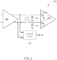
- FIG. 2 is a diagram illustrating a power amplifier system 200 according to one embodiment of the present invention.
- the power amplifier system 200 comprises a power amplifier 210, two varactors (varactor diode) 222 and 224, a control circuit 230 and a driver 240.
- the power amplifier 210 receives a differential input signal Vin (radio frequency (RF) signal) from the driver 240 to generate a differential output.
- the control circuit 230 is arranged to receive the input signal Vin to generate a bias voltage Vb, where a voltage level of the bias voltage Vb is changed with a power of the input signal Vin.
- RF radio frequency
- a first node of the varactor 222/224 is coupled to an input terminal of the power amplifier 210, which is biased by a fixed DC voltage, and a second node of the varactor 222/224 is biased by the bias voltage Vb generated by the control circuit 230.
- the capacitances of the varactors 222 and 224 are changed in response to the power of the input signal Vin, to compensate the nonlinear input capacitance of the power amplifier 210 shown in FIG. 1 .
- FIG. 3 is a diagram illustrating the control circuit 230 according to one embodiment of the present invention.
- the control circuit 230 comprises an attenuator 310, a peak detector 320, one or more rising comparator(s) 332, a programmable current source 334, one or more falling comparator(s) 342, a programmable current source 344, and a bias circuit 350.
- the attenuator 310 attenuates the input signal Vin.
- the peak detector 320 detects the amplitude of the attenuated input signal Vin.
- the rising comparator 332 compares the amplitude of the input signal with a first threshold to generate a first comparing result, and the programmable current source 334 generates a first current according to the first comparing result.
- the falling comparator 342 compares the amplitude of the input signal with a second threshold to generate a second comparing result, and the programmable current source 344 generates a second current according to the second comparing result. Then, an output current is generated according to the first current and the second current.
- the bias circuit 350 performs an I-to-V conversion upon the output current to generate the bias voltage Vb.
- FIG. 4 is a detailed structure of the control circuit 230 according to one embodiment of the present invention.
- the input signal may comprise a positive input signal Vin+ and a negative input signal Vin+
- the attenuator 310 can be implemented by a capacitance divider comprising two capacitors C1 and C2 and two variable capacitors C3 and C4.
- the peak detector 320 comprises two transistors M1 and M2 biased by a voltage Vb1 through resistors R1 and R2, and a voltage Vc of a drain electrode of a transistor M3 is used to represent the amplitude of the input signal Vin (attenuated input signal).
- the rising comparator 332 is implemented by transistors M4-M6, and the rising comparator 332 compares the voltage Vc with the first threshold TH1 to generate the first comparing result to control/adjust the first current generated by the programmable current source 334, where the programmable current source 334 comprises a current source 402 and a switch SW1.
- the falling comparator 342 is implemented by transistors M7-M9, and the falling comparator 342 compares the voltage Vc with the second threshold TH2 to generate the second comparing result to control/adjust the second current generated by the programmable current source 344 via transistors M10 and M11, where the programmable current source 344 comprises a current source 404 and a switch SW2.
- the programmable current source 334 is used to provide the first current to an output node Nc
- the programmable current source 344 is used to sink the second current from the output node Nc, that is, the output node Nc can be regarded as a combiner to generate an output current by subtracting the second current from the first current.
- the output current at the output node Nc is represented as "I+ ⁇ I” in FIG. 4 .
- a DC replica circuit 410 is used to remove a DC current (e.g. "I") from the output current "I+ ⁇ I”.
- the bias circuit 350 performs an I-to-V conversion upon the current " ⁇ I" to generate the bias voltage Vb.
- the first threshold TH1, the second threshold TH2, and currents provided by the current sources 402 and 404 can be set by an engineer to have a suitable input capacitance compensation for the power amplifier 210.
- the first threshold TH1 may be 0.5V
- the second threshold TH2 may be 1V
- the current provided by the current source 402 may be ten times the current provided by the current source 404
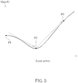
- the bias voltage Vb may have a V-shaped curve while the amplifier of the input signal Vin increases as shown in FIG. 5 .
- the capacitance of the varactors 222 and 224 can be adaptively controlled to compensate the nonlinearity of the input capacitance (AM-PM distortion) of the power amplifier 210. Therefore, the input capacitance of the power amplifier 210 can be more stable, and the efficiency of the power amplifier 210 can be improved.
- the control circuit 230 does not have any operational amplifier, therefore a bandwidth of the power amplifier system 200 can increase.
- the engineer can set many different curves (e.g. different positions of the points P1-P3) for the power amplifiers having different nonlinearity input capacitance curves.
- the peak detector 310 is used to detect the amplitude of the input signal Vin outputted by the driver 240. In other embodiments, however, the peak detector 310 can detect an input of the power amplifier 210, or detect an output of the power amplifier 210 to generate a detecting result to the rising comparator 332 and the falling comparator 342. These alternative designs shall fall within the scope of the present invention.
- FIG. 7 is a flowchart of a method for compensating an input capacitance of a power amplifier according to one embodiment of the present invention. Referring to FIG. 7 and the aforementioned embodiments, the flow is as follows.
- Step 700 The flow starts.
- Step 702 detect an amplitude of an input signal.
- Step 704 compare the amplitude of the input signal with a first threshold to generate a first comparing result.
- Step 706 generate a first current according to the first comparing result.
- Step 708 compare the amplitude of the input signal with a second threshold to generate a second comparing result.
- Step 710 generate a second current according to the second comparing result.
- Step 712 generate a bias voltage according to the first current and the second current to compensate the input capacitance of the power amplifier.
- a varactor is used to compensate the nonlinearity of the input capacitance of the power amplifier, and a bias voltage provided to the varactor is determined based on an amplitude/power of a signal associated to the power amplifier. Therefore, the nonlinear input capacitance of the power amplifier can be efficiently compensated.
Landscapes
- Engineering & Computer Science (AREA)
- Power Engineering (AREA)
- Physics & Mathematics (AREA)
- Nonlinear Science (AREA)
- Microelectronics & Electronic Packaging (AREA)
- Amplifiers (AREA)
Abstract
Description
- As a wireless communication system becomes more complicated, a linearity of a power amplifier is more critical, and a spectral re-growth for compensating the power amplifier distortion has more challenge.
FIG. 1 shows a nonlinear input capacitance of the power amplifier due to the AM-PM distortion. As shown inFIG. 1 , when the input power increases, the input capacitance of the power amplifier may suddenly drop, and the efficiency of the power amplifier may be worsened. - It is therefore an objective of the present invention to provide a power amplifier system, which can efficiently compensate the nonlinear input capacitance of the power amplifier, to solve the above-mentioned problem.
- This is achieved by a control circuit of a power amplifier according to claim 1, a method for compensating an input capacitance of a power amplifier according to claim 9, and a power amplifier system according to claim 14. The dependent claims pertain to corresponding further developments and improvements.
- As will be seen more clearly from the detailed description following below, a control circuit of a power amplifier comprises a peak detector, at least a first comparator, a first current source, at least a second comparator, a second current source and a bias circuit. The peak detector is arranged for detecting an amplitude of an input signal. The first comparator is coupled to the peak detector, and is arranged for comparing the amplitude of the input signal with a first threshold to generate a first comparing result. The first current source is coupled to the first comparator, and is arranged for generating a first current according to the first comparing result. The second comparator is coupled to the peak detector, and is arranged for comparing the amplitude of the input signal with a second threshold to generate a second comparing result. The second current source is coupled to the second comparator, and is arranged for generating a second current according to the second comparing result. The bias circuit is coupled to the first current source and the second current source, and is arranged for generating a bias voltage according to the first current and the second current to the power amplifier.
- As will be seen more clearly from the detailed description following below, a method for compensating an input capacitance of a power amplifier comprises: detecting an amplitude of an input signal; comparing the amplitude of the input signal with a first threshold to generate a first comparing result; generating a first current according to the first comparing result; comparing the amplitude of the input signal with a second threshold to generate a second comparing result; generating a second current according to the second comparing result; and generating a bias voltage according to the first current and the second current to compensate the input capacitance of the power amplifier.
- As will be seen more clearly from the detailed description following below, a power amplifier system comprises a power amplifier, a varactor and a control circuit, where a first node of the varactor is coupled to an input terminal of the power amplifier; and the control circuit generates a bias voltage according to an amplitude of an input signal to a second node of the varactor, to compensate an input capacitance of the power amplifier.
- These and other objectives of the present invention will no doubt become obvious to those of ordinary skill in the art after reading the following detailed description of the preferred embodiment that is illustrated in the various figures and drawings.
-
-
FIG. 1 shows a nonlinear input capacitance of the power amplifier due to the AM-PM distortion. -
FIG. 2 is a diagram illustrating a power amplifier system according to one embodiment of the present invention. -
FIG. 3 is a diagram illustrating the control circuit according to one embodiment of the present invention. -
FIG. 4 is a detailed structure of the control circuit according to one embodiment of the present invention. -
FIG. 5 shows that the bias voltage is changed with the power of the input signal according to one embodiment of the present invention. -
FIG. 6 shows the changes of the capacitance of the varactor when the bias voltage changes with the power of the input signal according to one embodiment of the present invention. -
FIG. 7 is a flowchart of a method for compensating an input capacitance of a power amplifier according to one embodiment of the present invention. - Certain terms are used throughout the following description and claims to refer to particular system components. As one skilled in the art will appreciate, manufacturers may refer to a component by different names. This document does not intend to distinguish between components that differ in name but not function. In the following discussion and in the claims, the terms "including" and "comprising" are used in an open-ended fashion, and thus should be interpreted to mean "including, but not limited to ..." The terms "couple" and "couples" are intended to mean either an indirect or a direct electrical connection. Thus, if a first device couples to a second device, that connection may be through a direct electrical connection, or through an indirect electrical connection via other devices and connections.
- Please refer to
FIG. 2 , which is a diagram illustrating apower amplifier system 200 according to one embodiment of the present invention. InFIG. 2 , thepower amplifier system 200 comprises apower amplifier 210, two varactors (varactor diode) 222 and 224, acontrol circuit 230 and adriver 240. In the operations of thepower amplifier system 200, thepower amplifier 210 receives a differential input signal Vin (radio frequency (RF) signal) from thedriver 240 to generate a differential output. Thecontrol circuit 230 is arranged to receive the input signal Vin to generate a bias voltage Vb, where a voltage level of the bias voltage Vb is changed with a power of the input signal Vin. In this embodiment, a first node of thevaractor 222/224 is coupled to an input terminal of thepower amplifier 210, which is biased by a fixed DC voltage, and a second node of thevaractor 222/224 is biased by the bias voltage Vb generated by thecontrol circuit 230. In light of above, the capacitances of thevaractors power amplifier 210 shown inFIG. 1 . - Please refer to
FIG. 3 , which is a diagram illustrating thecontrol circuit 230 according to one embodiment of the present invention. As shown inFIG. 3 , thecontrol circuit 230 comprises anattenuator 310, apeak detector 320, one or more rising comparator(s) 332, a programmablecurrent source 334, one or more falling comparator(s) 342, a programmablecurrent source 344, and abias circuit 350. In the operations of thecontrol circuit 230, first, theattenuator 310 attenuates the input signal Vin. Then, thepeak detector 320 detects the amplitude of the attenuated input signal Vin. The risingcomparator 332 compares the amplitude of the input signal with a first threshold to generate a first comparing result, and the programmablecurrent source 334 generates a first current according to the first comparing result. The fallingcomparator 342 compares the amplitude of the input signal with a second threshold to generate a second comparing result, and the programmablecurrent source 344 generates a second current according to the second comparing result. Then, an output current is generated according to the first current and the second current. Finally, thebias circuit 350 performs an I-to-V conversion upon the output current to generate the bias voltage Vb. - In detail,
FIG. 4 is a detailed structure of thecontrol circuit 230 according to one embodiment of the present invention. As shown inFIG. 4 , the input signal may comprise a positive input signal Vin+ and a negative input signal Vin+, and theattenuator 310 can be implemented by a capacitance divider comprising two capacitors C1 and C2 and two variable capacitors C3 and C4. Thepeak detector 320 comprises two transistors M1 and M2 biased by a voltage Vb1 through resistors R1 and R2, and a voltage Vc of a drain electrode of a transistor M3 is used to represent the amplitude of the input signal Vin (attenuated input signal). The risingcomparator 332 is implemented by transistors M4-M6, and the risingcomparator 332 compares the voltage Vc with the first threshold TH1 to generate the first comparing result to control/adjust the first current generated by the programmablecurrent source 334, where the programmablecurrent source 334 comprises acurrent source 402 and a switch SW1. The fallingcomparator 342 is implemented by transistors M7-M9, and the fallingcomparator 342 compares the voltage Vc with the second threshold TH2 to generate the second comparing result to control/adjust the second current generated by the programmablecurrent source 344 via transistors M10 and M11, where the programmablecurrent source 344 comprises acurrent source 404 and a switch SW2. In this embodiment, the programmablecurrent source 334 is used to provide the first current to an output node Nc, and the programmablecurrent source 344 is used to sink the second current from the output node Nc, that is, the output node Nc can be regarded as a combiner to generate an output current by subtracting the second current from the first current. The output current at the output node Nc is represented as "I+ΔI" inFIG. 4 . Then, aDC replica circuit 410 is used to remove a DC current (e.g. "I") from the output current "I+ΔI". Finally, thebias circuit 350 performs an I-to-V conversion upon the current "ΔI" to generate the bias voltage Vb. - In the embodiment shown in
FIG. 4 , the first threshold TH1, the second threshold TH2, and currents provided by thecurrent sources power amplifier 210. For example, the first threshold TH1 may be 0.5V, the second threshold TH2 may be 1V, and the current provided by thecurrent source 402 may be ten times the current provided by thecurrent source 404, and the bias voltage Vb may have a V-shaped curve while the amplifier of the input signal Vin increases as shown inFIG. 5 . That is, when the amplifier of the input signal Vin increases, first the output current "I+ΔI" decreases to decrease the bias voltage Vb (from a point P1 to a point P2), and then the output current "I+ΔI" increases to increase the bias voltage Vb (from the point P2 to a point P3). Therefore, because of the special curve of the bias voltage Vb shown inFIG. 5 , when the amplifier/power of the input signal Vin continuously increases, the capacitance of thevaractors FIG. 1 , and then the capacitance of thevaractors FIG. 6 . - By using the embodiments mentioned above, the capacitance of the
varactors power amplifier 210. Therefore, the input capacitance of thepower amplifier 210 can be more stable, and the efficiency of thepower amplifier 210 can be improved. - In the embodiment shown in
FIG. 4 , thecontrol circuit 230 does not have any operational amplifier, therefore a bandwidth of thepower amplifier system 200 can increase. In addition, because the first threshold TH1, the second threshold TH2, and currents provided by thecurrent sources - In addition, in the embodiments shown in
FIG. 2-4 , thepeak detector 310 is used to detect the amplitude of the input signal Vin outputted by thedriver 240. In other embodiments, however, thepeak detector 310 can detect an input of thepower amplifier 210, or detect an output of thepower amplifier 210 to generate a detecting result to the risingcomparator 332 and the fallingcomparator 342. These alternative designs shall fall within the scope of the present invention. - Please refer to
FIG. 7 , which is a flowchart of a method for compensating an input capacitance of a power amplifier according to one embodiment of the present invention. Referring toFIG. 7 and the aforementioned embodiments, the flow is as follows. - Step 700: The flow starts.
- Step 702: detect an amplitude of an input signal.
- Step 704: compare the amplitude of the input signal with a first threshold to generate a first comparing result.
- Step 706: generate a first current according to the first comparing result.
- Step 708: compare the amplitude of the input signal with a second threshold to generate a second comparing result.
- Step 710: generate a second current according to the second comparing result.
- Step 712: generate a bias voltage according to the first current and the second current to compensate the input capacitance of the power amplifier.
- Briefly summarized, in the power amplifier system of the present invention, a varactor is used to compensate the nonlinearity of the input capacitance of the power amplifier, and a bias voltage provided to the varactor is determined based on an amplitude/power of a signal associated to the power amplifier. Therefore, the nonlinear input capacitance of the power amplifier can be efficiently compensated.
- Those skilled in the art will readily observe that numerous modifications and alterations of the device and method may be made while retaining the teachings of the invention. Accordingly, the above disclosure should be construed as limited only by the metes and bounds of the appended claims.
Claims (15)
- A control circuit (230) of a power amplifier (210), characterized by:a peak detector (320), for detecting an amplitude of an input signal;at least a first comparator (332), coupled to the peak detector (320), for comparing the amplitude of the input signal with a first threshold to generate a first comparing result;a first current source (334), coupled to the first comparator (332), for generating a first current according to the first comparing result;at least a second comparator (342), coupled to the peak detector (320), for comparing the amplitude of the input signal with a second threshold to generate a second comparing result;a second current source (344), coupled to the second comparator (342), for generating a second current according to the second comparing result; anda bias circuit (350), coupled to the first current source (334) and the second current source (344), for generating a bias voltage according to the first current and the second current to the power amplifier (210).
- The control circuit (230) of claim 1, characterized in that the bias circuit (350) generates the bias voltage to a varactor (222, 224) connected to an input terminal of the power amplifier (210), to control a capacitance of the varactor (222, 224).
- The control circuit (230) of claim 2, characterized in that when the amplitude of the input signal continuously increases, the bias circuit (350) generates the bias voltage to increases the capacitance of the varactor (222, 224), and then to decrease the capacitance of the varactor (222, 224).
- The control circuit (230) of claim 3, characterized in that a first node of the varactor (222, 224) is connected to the input terminal of the power amplifier (210), and a second node of the varactor (222, 224) is arranged to receive the bias voltage; and when the amplitude of the input signal continuously increases, first the bias circuit (350) decreases the bias voltage to increase the capacitance of the varactor (222, 224), and then the bias circuit (350) increases the bias voltage to decrease the capacitance of the varactor (222, 224).
- The control circuit (230) of claim 1, characterized in that the bias circuit (350) generates the bias voltage according to a difference between the first current and the second current.
- The control circuit (230) of claim 5, characterized in that further comprising:a combiner (Nc), coupled between the first current source (334) and the second current source (344), for generating an output current by subtracting the second current from the first current;wherein the bias circuit (350) generates the bias voltage according to the output current.
- The control circuit (230) of claim 6, characterized in that when the amplitude of the input signal continuously increases, first the output current decreases to decrease the bias voltage, and then the output current increases to increase the bias voltage, so as to compensate an input capacitance of the power amplifier (210).
- The control circuit (230) of claim 7, characterized in that the bias circuit (350) generates the bias voltage to a varactor (222, 224) connected to an input terminal of the power amplifier (210), to control a capacitance of the varactor (222, 224) to compensate the input capacitance of the power amplifier (210).
- A method for compensating an input capacitance of a power amplifier (210), characterized by the method comprises the steps of:detecting an amplitude of an input signal;comparing the amplitude of the input signal with a first threshold to generate a first comparing result;generating a first current according to the first comparing result;comparing the amplitude of the input signal with a second threshold to generate a second comparing result;generating a second current according to the second comparing result; andgenerating a bias voltage according to the first current and the second current to compensate the input capacitance of the power amplifier (210).
- The method of claim 9, characterized in that the step of generating the bias voltage according to the first current and the second current to compensate the input capacitance of the power amplifier (210) comprises:generating the bias voltage to a varactor (222, 224) connected to an input terminal of the power amplifier (210), to control a capacitance of the varactor (222, 224) to compensate the input capacitance of the power amplifier (210).
- The method of claim 10, characterized in that the step of generating the bias voltage according to the first current and the second current to compensate the input capacitance of the power amplifier (210) comprises:when the amplitude of the input signal continuously increases, generating the bias voltage to increases the capacitance of the varactor (222, 224), and then decreasing the capacitance of the varactor (222, 224).
- The method of claim 11, characterized in that a first node of the varactor (222, 224) is connected to the input terminal of the power amplifier (210), and a second node of the varactor (222, 224) is arranged to receive the bias voltage, and the step of generating the bias voltage according to the first current and the second current to compensate the input capacitance of the power amplifier (210) comprises:when the amplitude of the input signal continuously increases, first decreasing the bias voltage to increase the capacitance of the varactor (222, 224), and then increasing the bias voltage to decrease the capacitance of the varactor (222, 224).
- The method of claim 9, characterized in that the step of generating the bias voltage according to the first current and the second current to compensate the input capacitance of the power amplifier (210) comprises:generating the bias voltage according to a difference between the first current and the second current to compensate the input capacitance of the power amplifier (210).
- A power amplifier system (200), comprising:a power amplifier (210);characterized by:a varactor (222, 224), wherein a first node of the varactor (222, 224) is coupled to an input terminal of the power amplifier (210); anda control circuit (230), for generating a bias voltage according to an amplitude of an input signal to a second node of the varactor (222, 224), to compensate an input capacitance of the power amplifier (210).
- The power amplifier system (200) of claim 14, characterized in that the control circuit (230) comprises:a peak detector (320), for detecting the amplitude of the input signal;at least a first comparator (332), coupled to the peak detector (320), for comparing the amplitude of the input signal with a first threshold to generate a first comparing result;a first current source (334), coupled to the first comparator (332), for generating a first current according to the first comparing result;at least a second comparator (342), coupled to the peak detector (320), for comparing the amplitude of the input signal with a second threshold to generate a second comparing result;a second current source (344), coupled to the second comparator (342), for generating a second current according to the second comparing result; anda bias circuit (350), coupled to the first current source (334) and the second current source (344), for generating the bias voltage according to the first current and the second current to the second node of the varactor (222, 224).
Applications Claiming Priority (2)
| Application Number | Priority Date | Filing Date | Title |
|---|---|---|---|
| US201662280716P | 2016-01-20 | 2016-01-20 | |
| US15/348,956 US10056869B2 (en) | 2016-01-20 | 2016-11-10 | Power amplifier system and associated control circuit and control method |
Publications (2)
| Publication Number | Publication Date |
|---|---|
| EP3197048A1 true EP3197048A1 (en) | 2017-07-26 |
| EP3197048B1 EP3197048B1 (en) | 2021-01-06 |
Family
ID=57326295
Family Applications (1)
| Application Number | Title | Priority Date | Filing Date |
|---|---|---|---|
| EP16199083.3A Active EP3197048B1 (en) | 2016-01-20 | 2016-11-16 | Power amplifier system and associated control circuit and control method |
Country Status (3)
| Country | Link |
|---|---|
| US (1) | US10056869B2 (en) |
| EP (1) | EP3197048B1 (en) |
| CN (1) | CN107017852B (en) |
Families Citing this family (6)
| Publication number | Priority date | Publication date | Assignee | Title |
|---|---|---|---|---|
| CN114520634B (en) * | 2020-11-19 | 2026-01-09 | 瑞昱半导体股份有限公司 | Transmitting circuit and its transmission signal strength adjustment method |
| CN112543005B (en) * | 2021-02-18 | 2021-06-04 | 广州慧智微电子有限公司 | Amplitude modulation to phase modulation compensation circuit, radio frequency power amplifier and equipment |
| CN112803905B (en) * | 2021-04-14 | 2021-09-28 | 广州慧智微电子有限公司 | Compensation circuit |
| US12028098B2 (en) * | 2021-09-13 | 2024-07-02 | Apple Inc. | Radio-frequency power amplifier with amplitude modulation to phase modulation (AMPM) compensation |
| US12483204B2 (en) * | 2022-03-29 | 2025-11-25 | Qorvo Us, Inc. | Power amplifier system |
| US12494745B2 (en) | 2022-04-14 | 2025-12-09 | Qorvo Us, Inc. | Amplitude modulation-phase modulation (AM-PM) linearization in a power amplifier |
Citations (4)
| Publication number | Priority date | Publication date | Assignee | Title |
|---|---|---|---|---|
| US20050184802A1 (en) * | 2004-02-25 | 2005-08-25 | Intel Corporation | Distortion management apparatus, systems, and methods |
| US20080303591A1 (en) * | 2007-06-06 | 2008-12-11 | Realtek Semiconductor Corp. | Amplifying circuit and associated linearity improving method |
| US20110074509A1 (en) * | 2008-03-31 | 2011-03-31 | Anil Samavedam | Non-linear capacitance compensation |
| US20140266432A1 (en) * | 2013-03-15 | 2014-09-18 | Rf Micro Devices (Cayman Islands), Ltd. | Amplifier phase distortion correction based on amplitude distortion measurement |
Family Cites Families (9)
| Publication number | Priority date | Publication date | Assignee | Title |
|---|---|---|---|---|
| US6893101B2 (en) * | 2001-07-27 | 2005-05-17 | Telefonaktiebolaget L.M. Ericsson | Active element bias circuit for RF power transistor input |
| US6828858B2 (en) | 2002-04-12 | 2004-12-07 | The Regents Of The University Of California | CMOS class AB power amplifier with cancellation of nonlinearity due to change in gate capacitance of a NMOS input transistor with switching |
| WO2005079313A2 (en) | 2004-02-13 | 2005-09-01 | The Regents Of The University Of California | Adaptive bias current circuit and method for amplifiers |
| US8787850B2 (en) | 2008-03-31 | 2014-07-22 | Avago Technologies General Ip (Singapore) Pte. Ltd. | Compensating for non-linear capacitance effects in a power amplifier |
| US8299852B2 (en) * | 2010-03-09 | 2012-10-30 | Ronald Quan | Method and apparatus for a gain control circuit via a high frequency signal |
| KR101763410B1 (en) * | 2010-12-21 | 2017-08-04 | 한국전자통신연구원 | Digital Pre-distortion Power Amplifier and Method for Controlling Sync Digitally thereof |
| US9054062B2 (en) * | 2011-03-04 | 2015-06-09 | Peregrine Semiconductor Corporation | Systems and methods for current sensing over an extended area |
| US9236837B2 (en) * | 2011-08-25 | 2016-01-12 | Infineon Technologies Ag | System and method for low distortion capacitive signal source amplifier |
| JP5624569B2 (en) * | 2012-02-17 | 2014-11-12 | 株式会社東芝 | Power amplifier |
-
2016
- 2016-11-10 US US15/348,956 patent/US10056869B2/en active Active
- 2016-11-16 EP EP16199083.3A patent/EP3197048B1/en active Active
-
2017
- 2017-01-05 CN CN201710006468.5A patent/CN107017852B/en active Active
Patent Citations (4)
| Publication number | Priority date | Publication date | Assignee | Title |
|---|---|---|---|---|
| US20050184802A1 (en) * | 2004-02-25 | 2005-08-25 | Intel Corporation | Distortion management apparatus, systems, and methods |
| US20080303591A1 (en) * | 2007-06-06 | 2008-12-11 | Realtek Semiconductor Corp. | Amplifying circuit and associated linearity improving method |
| US20110074509A1 (en) * | 2008-03-31 | 2011-03-31 | Anil Samavedam | Non-linear capacitance compensation |
| US20140266432A1 (en) * | 2013-03-15 | 2014-09-18 | Rf Micro Devices (Cayman Islands), Ltd. | Amplifier phase distortion correction based on amplitude distortion measurement |
Also Published As
| Publication number | Publication date |
|---|---|
| US10056869B2 (en) | 2018-08-21 |
| EP3197048B1 (en) | 2021-01-06 |
| CN107017852A (en) | 2017-08-04 |
| CN107017852B (en) | 2020-09-18 |
| US20170207758A1 (en) | 2017-07-20 |
Similar Documents
| Publication | Publication Date | Title |
|---|---|---|
| EP3197048B1 (en) | Power amplifier system and associated control circuit and control method | |
| KR101645729B1 (en) | Voltage regulator | |
| US20110012682A1 (en) | Electronic circuit with cascode amplifier | |
| US20140253243A1 (en) | Power amplifying module | |
| CN104641553A (en) | Power amplification module | |
| US8508200B2 (en) | Power supply circuit using amplifiers and current voltage converter for improving ripple removal rate and differential balance | |
| US10516370B2 (en) | Predistorter for compensating linearity of an amplifier | |
| US8432228B1 (en) | Power control circuit for radio frequency power amplifiers | |
| US20140112414A1 (en) | Power amplifier and the related power amplifying method | |
| US9276565B2 (en) | Duty ratio correction circuit and phase synchronization circuit | |
| CN110690861A (en) | Multi-stage power amplifier with linear compensation function | |
| US7696822B2 (en) | Amplifying circuit and associated linearity improving method | |
| JP2007295531A (en) | Electronic circuit | |
| US9960947B2 (en) | Compensation circuit of power amplifier and associated compensation method | |
| US10461702B2 (en) | Amplifier circuit having poly resistor with biased depletion region | |
| JP2006093896A (en) | Class E amplifier and EER modulation amplifier | |
| US8536942B2 (en) | Power amplifier | |
| CN117674745A (en) | Amplifying circuit and communication device | |
| US11595010B2 (en) | Optical receiver and transimpedance amplifier circuit | |
| US9768630B2 (en) | Real time compensating power output charging circuit | |
| KR101503971B1 (en) | Power detection circuit | |
| US20200036347A1 (en) | Source follower | |
| JP2007159020A (en) | Current-voltage conversion circuit | |
| TWI693788B (en) | Predistorter for compensating linearity of amplifier | |
| JPWO2016047090A1 (en) | Output power control device |
Legal Events
| Date | Code | Title | Description |
|---|---|---|---|
| PUAI | Public reference made under article 153(3) epc to a published international application that has entered the european phase |
Free format text: ORIGINAL CODE: 0009012 |
|
| STAA | Information on the status of an ep patent application or granted ep patent |
Free format text: STATUS: THE APPLICATION HAS BEEN PUBLISHED |
|
| AK | Designated contracting states |
Kind code of ref document: A1 Designated state(s): AL AT BE BG CH CY CZ DE DK EE ES FI FR GB GR HR HU IE IS IT LI LT LU LV MC MK MT NL NO PL PT RO RS SE SI SK SM TR |
|
| AX | Request for extension of the european patent |
Extension state: BA ME |
|
| STAA | Information on the status of an ep patent application or granted ep patent |
Free format text: STATUS: REQUEST FOR EXAMINATION WAS MADE |
|
| 17P | Request for examination filed |
Effective date: 20170830 |
|
| RBV | Designated contracting states (corrected) |
Designated state(s): AL AT BE BG CH CY CZ DE DK EE ES FI FR GB GR HR HU IE IS IT LI LT LU LV MC MK MT NL NO PL PT RO RS SE SI SK SM TR |
|
| STAA | Information on the status of an ep patent application or granted ep patent |
Free format text: STATUS: EXAMINATION IS IN PROGRESS |
|
| 17Q | First examination report despatched |
Effective date: 20200319 |
|
| GRAP | Despatch of communication of intention to grant a patent |
Free format text: ORIGINAL CODE: EPIDOSNIGR1 |
|
| STAA | Information on the status of an ep patent application or granted ep patent |
Free format text: STATUS: GRANT OF PATENT IS INTENDED |
|
| INTG | Intention to grant announced |
Effective date: 20201020 |
|
| GRAS | Grant fee paid |
Free format text: ORIGINAL CODE: EPIDOSNIGR3 |
|
| GRAA | (expected) grant |
Free format text: ORIGINAL CODE: 0009210 |
|
| STAA | Information on the status of an ep patent application or granted ep patent |
Free format text: STATUS: THE PATENT HAS BEEN GRANTED |
|
| AK | Designated contracting states |
Kind code of ref document: B1 Designated state(s): AL AT BE BG CH CY CZ DE DK EE ES FI FR GB GR HR HU IE IS IT LI LT LU LV MC MK MT NL NO PL PT RO RS SE SI SK SM TR |
|
| REG | Reference to a national code |
Ref country code: GB Ref legal event code: FG4D |
|
| REG | Reference to a national code |
Ref country code: AT Ref legal event code: REF Ref document number: 1353465 Country of ref document: AT Kind code of ref document: T Effective date: 20210115 Ref country code: CH Ref legal event code: EP |
|
| REG | Reference to a national code |
Ref country code: DE Ref legal event code: R096 Ref document number: 602016050925 Country of ref document: DE |
|
| REG | Reference to a national code |
Ref country code: IE Ref legal event code: FG4D |
|
| REG | Reference to a national code |
Ref country code: NL Ref legal event code: MP Effective date: 20210106 |
|
| REG | Reference to a national code |
Ref country code: AT Ref legal event code: MK05 Ref document number: 1353465 Country of ref document: AT Kind code of ref document: T Effective date: 20210106 |
|
| REG | Reference to a national code |
Ref country code: LT Ref legal event code: MG9D |
|
| PG25 | Lapsed in a contracting state [announced via postgrant information from national office to epo] |
Ref country code: PT Free format text: LAPSE BECAUSE OF FAILURE TO SUBMIT A TRANSLATION OF THE DESCRIPTION OR TO PAY THE FEE WITHIN THE PRESCRIBED TIME-LIMIT Effective date: 20210506 Ref country code: NO Free format text: LAPSE BECAUSE OF FAILURE TO SUBMIT A TRANSLATION OF THE DESCRIPTION OR TO PAY THE FEE WITHIN THE PRESCRIBED TIME-LIMIT Effective date: 20210406 Ref country code: FI Free format text: LAPSE BECAUSE OF FAILURE TO SUBMIT A TRANSLATION OF THE DESCRIPTION OR TO PAY THE FEE WITHIN THE PRESCRIBED TIME-LIMIT Effective date: 20210106 Ref country code: GR Free format text: LAPSE BECAUSE OF FAILURE TO SUBMIT A TRANSLATION OF THE DESCRIPTION OR TO PAY THE FEE WITHIN THE PRESCRIBED TIME-LIMIT Effective date: 20210407 Ref country code: HR Free format text: LAPSE BECAUSE OF FAILURE TO SUBMIT A TRANSLATION OF THE DESCRIPTION OR TO PAY THE FEE WITHIN THE PRESCRIBED TIME-LIMIT Effective date: 20210106 Ref country code: BG Free format text: LAPSE BECAUSE OF FAILURE TO SUBMIT A TRANSLATION OF THE DESCRIPTION OR TO PAY THE FEE WITHIN THE PRESCRIBED TIME-LIMIT Effective date: 20210406 Ref country code: NL Free format text: LAPSE BECAUSE OF FAILURE TO SUBMIT A TRANSLATION OF THE DESCRIPTION OR TO PAY THE FEE WITHIN THE PRESCRIBED TIME-LIMIT Effective date: 20210106 Ref country code: LT Free format text: LAPSE BECAUSE OF FAILURE TO SUBMIT A TRANSLATION OF THE DESCRIPTION OR TO PAY THE FEE WITHIN THE PRESCRIBED TIME-LIMIT Effective date: 20210106 |
|
| PG25 | Lapsed in a contracting state [announced via postgrant information from national office to epo] |
Ref country code: SE Free format text: LAPSE BECAUSE OF FAILURE TO SUBMIT A TRANSLATION OF THE DESCRIPTION OR TO PAY THE FEE WITHIN THE PRESCRIBED TIME-LIMIT Effective date: 20210106 Ref country code: RS Free format text: LAPSE BECAUSE OF FAILURE TO SUBMIT A TRANSLATION OF THE DESCRIPTION OR TO PAY THE FEE WITHIN THE PRESCRIBED TIME-LIMIT Effective date: 20210106 Ref country code: LV Free format text: LAPSE BECAUSE OF FAILURE TO SUBMIT A TRANSLATION OF THE DESCRIPTION OR TO PAY THE FEE WITHIN THE PRESCRIBED TIME-LIMIT Effective date: 20210106 Ref country code: PL Free format text: LAPSE BECAUSE OF FAILURE TO SUBMIT A TRANSLATION OF THE DESCRIPTION OR TO PAY THE FEE WITHIN THE PRESCRIBED TIME-LIMIT Effective date: 20210106 Ref country code: AT Free format text: LAPSE BECAUSE OF FAILURE TO SUBMIT A TRANSLATION OF THE DESCRIPTION OR TO PAY THE FEE WITHIN THE PRESCRIBED TIME-LIMIT Effective date: 20210106 |
|
| PG25 | Lapsed in a contracting state [announced via postgrant information from national office to epo] |
Ref country code: IS Free format text: LAPSE BECAUSE OF FAILURE TO SUBMIT A TRANSLATION OF THE DESCRIPTION OR TO PAY THE FEE WITHIN THE PRESCRIBED TIME-LIMIT Effective date: 20210506 |
|
| REG | Reference to a national code |
Ref country code: DE Ref legal event code: R097 Ref document number: 602016050925 Country of ref document: DE |
|
| PG25 | Lapsed in a contracting state [announced via postgrant information from national office to epo] |
Ref country code: CZ Free format text: LAPSE BECAUSE OF FAILURE TO SUBMIT A TRANSLATION OF THE DESCRIPTION OR TO PAY THE FEE WITHIN THE PRESCRIBED TIME-LIMIT Effective date: 20210106 Ref country code: EE Free format text: LAPSE BECAUSE OF FAILURE TO SUBMIT A TRANSLATION OF THE DESCRIPTION OR TO PAY THE FEE WITHIN THE PRESCRIBED TIME-LIMIT Effective date: 20210106 Ref country code: SM Free format text: LAPSE BECAUSE OF FAILURE TO SUBMIT A TRANSLATION OF THE DESCRIPTION OR TO PAY THE FEE WITHIN THE PRESCRIBED TIME-LIMIT Effective date: 20210106 |
|
| PLBE | No opposition filed within time limit |
Free format text: ORIGINAL CODE: 0009261 |
|
| STAA | Information on the status of an ep patent application or granted ep patent |
Free format text: STATUS: NO OPPOSITION FILED WITHIN TIME LIMIT |
|
| PG25 | Lapsed in a contracting state [announced via postgrant information from national office to epo] |
Ref country code: DK Free format text: LAPSE BECAUSE OF FAILURE TO SUBMIT A TRANSLATION OF THE DESCRIPTION OR TO PAY THE FEE WITHIN THE PRESCRIBED TIME-LIMIT Effective date: 20210106 Ref country code: SK Free format text: LAPSE BECAUSE OF FAILURE TO SUBMIT A TRANSLATION OF THE DESCRIPTION OR TO PAY THE FEE WITHIN THE PRESCRIBED TIME-LIMIT Effective date: 20210106 Ref country code: RO Free format text: LAPSE BECAUSE OF FAILURE TO SUBMIT A TRANSLATION OF THE DESCRIPTION OR TO PAY THE FEE WITHIN THE PRESCRIBED TIME-LIMIT Effective date: 20210106 |
|
| 26N | No opposition filed |
Effective date: 20211007 |
|
| PG25 | Lapsed in a contracting state [announced via postgrant information from national office to epo] |
Ref country code: AL Free format text: LAPSE BECAUSE OF FAILURE TO SUBMIT A TRANSLATION OF THE DESCRIPTION OR TO PAY THE FEE WITHIN THE PRESCRIBED TIME-LIMIT Effective date: 20210106 Ref country code: ES Free format text: LAPSE BECAUSE OF FAILURE TO SUBMIT A TRANSLATION OF THE DESCRIPTION OR TO PAY THE FEE WITHIN THE PRESCRIBED TIME-LIMIT Effective date: 20210106 |
|
| PG25 | Lapsed in a contracting state [announced via postgrant information from national office to epo] |
Ref country code: SI Free format text: LAPSE BECAUSE OF FAILURE TO SUBMIT A TRANSLATION OF THE DESCRIPTION OR TO PAY THE FEE WITHIN THE PRESCRIBED TIME-LIMIT Effective date: 20210106 |
|
| PG25 | Lapsed in a contracting state [announced via postgrant information from national office to epo] |
Ref country code: IT Free format text: LAPSE BECAUSE OF FAILURE TO SUBMIT A TRANSLATION OF THE DESCRIPTION OR TO PAY THE FEE WITHIN THE PRESCRIBED TIME-LIMIT Effective date: 20210106 |
|
| PG25 | Lapsed in a contracting state [announced via postgrant information from national office to epo] |
Ref country code: IS Free format text: LAPSE BECAUSE OF FAILURE TO SUBMIT A TRANSLATION OF THE DESCRIPTION OR TO PAY THE FEE WITHIN THE PRESCRIBED TIME-LIMIT Effective date: 20210506 |
|
| PG25 | Lapsed in a contracting state [announced via postgrant information from national office to epo] |
Ref country code: MC Free format text: LAPSE BECAUSE OF FAILURE TO SUBMIT A TRANSLATION OF THE DESCRIPTION OR TO PAY THE FEE WITHIN THE PRESCRIBED TIME-LIMIT Effective date: 20210106 |
|
| REG | Reference to a national code |
Ref country code: CH Ref legal event code: PL |
|
| PG25 | Lapsed in a contracting state [announced via postgrant information from national office to epo] |
Ref country code: LU Free format text: LAPSE BECAUSE OF NON-PAYMENT OF DUE FEES Effective date: 20211116 Ref country code: BE Free format text: LAPSE BECAUSE OF NON-PAYMENT OF DUE FEES Effective date: 20211130 |
|
| REG | Reference to a national code |
Ref country code: BE Ref legal event code: MM Effective date: 20211130 |
|
| PG25 | Lapsed in a contracting state [announced via postgrant information from national office to epo] |
Ref country code: IE Free format text: LAPSE BECAUSE OF NON-PAYMENT OF DUE FEES Effective date: 20211116 |
|
| PG25 | Lapsed in a contracting state [announced via postgrant information from national office to epo] |
Ref country code: HU Free format text: LAPSE BECAUSE OF FAILURE TO SUBMIT A TRANSLATION OF THE DESCRIPTION OR TO PAY THE FEE WITHIN THE PRESCRIBED TIME-LIMIT; INVALID AB INITIO Effective date: 20161116 |
|
| PG25 | Lapsed in a contracting state [announced via postgrant information from national office to epo] |
Ref country code: CY Free format text: LAPSE BECAUSE OF FAILURE TO SUBMIT A TRANSLATION OF THE DESCRIPTION OR TO PAY THE FEE WITHIN THE PRESCRIBED TIME-LIMIT Effective date: 20210106 |
|
| P01 | Opt-out of the competence of the unified patent court (upc) registered |
Effective date: 20230607 |
|
| PG25 | Lapsed in a contracting state [announced via postgrant information from national office to epo] |
Ref country code: LI Free format text: LAPSE BECAUSE OF NON-PAYMENT OF DUE FEES Effective date: 20220701 Ref country code: CH Free format text: LAPSE BECAUSE OF NON-PAYMENT OF DUE FEES Effective date: 20220701 |
|
| PG25 | Lapsed in a contracting state [announced via postgrant information from national office to epo] |
Ref country code: MK Free format text: LAPSE BECAUSE OF FAILURE TO SUBMIT A TRANSLATION OF THE DESCRIPTION OR TO PAY THE FEE WITHIN THE PRESCRIBED TIME-LIMIT Effective date: 20210106 |
|
| PG25 | Lapsed in a contracting state [announced via postgrant information from national office to epo] |
Ref country code: TR Free format text: LAPSE BECAUSE OF FAILURE TO SUBMIT A TRANSLATION OF THE DESCRIPTION OR TO PAY THE FEE WITHIN THE PRESCRIBED TIME-LIMIT Effective date: 20210106 |
|
| PG25 | Lapsed in a contracting state [announced via postgrant information from national office to epo] |
Ref country code: MT Free format text: LAPSE BECAUSE OF FAILURE TO SUBMIT A TRANSLATION OF THE DESCRIPTION OR TO PAY THE FEE WITHIN THE PRESCRIBED TIME-LIMIT Effective date: 20210106 |
|
| PGFP | Annual fee paid to national office [announced via postgrant information from national office to epo] |
Ref country code: GB Payment date: 20250925 Year of fee payment: 10 |
|
| PGFP | Annual fee paid to national office [announced via postgrant information from national office to epo] |
Ref country code: FR Payment date: 20250908 Year of fee payment: 10 |
|
| PGFP | Annual fee paid to national office [announced via postgrant information from national office to epo] |
Ref country code: DE Payment date: 20250923 Year of fee payment: 10 |