EP3196927A1 - Joined body manufacturing method, multilayer joined body manufacturing method, power-module substrate manufacturing method, heat sink equipped power-module substrate manufacturing method, and laminated body manufacturing device - Google Patents
Joined body manufacturing method, multilayer joined body manufacturing method, power-module substrate manufacturing method, heat sink equipped power-module substrate manufacturing method, and laminated body manufacturing device Download PDFInfo
- Publication number
- EP3196927A1 EP3196927A1 EP15815025.0A EP15815025A EP3196927A1 EP 3196927 A1 EP3196927 A1 EP 3196927A1 EP 15815025 A EP15815025 A EP 15815025A EP 3196927 A1 EP3196927 A1 EP 3196927A1
- Authority
- EP
- European Patent Office
- Prior art keywords
- temporary fixing
- joining
- fixing material
- manufacturing
- module substrate
- Prior art date
- Legal status (The legal status is an assumption and is not a legal conclusion. Google has not performed a legal analysis and makes no representation as to the accuracy of the status listed.)
- Granted
Links
Images




Classifications
-
- H—ELECTRICITY
- H10—SEMICONDUCTOR DEVICES; ELECTRIC SOLID-STATE DEVICES NOT OTHERWISE PROVIDED FOR
- H10W—GENERIC PACKAGES, INTERCONNECTIONS, CONNECTORS OR OTHER CONSTRUCTIONAL DETAILS OF DEVICES COVERED BY CLASS H10
- H10W40/00—Arrangements for thermal protection or thermal control
- H10W40/20—Arrangements for cooling
- H10W40/25—Arrangements for cooling characterised by their materials
- H10W40/255—Arrangements for cooling characterised by their materials having a laminate or multilayered structure, e.g. direct bond copper [DBC] ceramic substrates
-
- H—ELECTRICITY
- H10—SEMICONDUCTOR DEVICES; ELECTRIC SOLID-STATE DEVICES NOT OTHERWISE PROVIDED FOR
- H10W—GENERIC PACKAGES, INTERCONNECTIONS, CONNECTORS OR OTHER CONSTRUCTIONAL DETAILS OF DEVICES COVERED BY CLASS H10
- H10W40/00—Arrangements for thermal protection or thermal control
- H10W40/20—Arrangements for cooling
- H10W40/22—Arrangements for cooling characterised by their shape, e.g. having conical or cylindrical projections
-
- B—PERFORMING OPERATIONS; TRANSPORTING
- B32—LAYERED PRODUCTS
- B32B—LAYERED PRODUCTS, i.e. PRODUCTS BUILT-UP OF STRATA OF FLAT OR NON-FLAT, e.g. CELLULAR OR HONEYCOMB, FORM
- B32B15/00—Layered products comprising a layer of metal
-
- B—PERFORMING OPERATIONS; TRANSPORTING
- B32—LAYERED PRODUCTS
- B32B—LAYERED PRODUCTS, i.e. PRODUCTS BUILT-UP OF STRATA OF FLAT OR NON-FLAT, e.g. CELLULAR OR HONEYCOMB, FORM
- B32B15/00—Layered products comprising a layer of metal
- B32B15/04—Layered products comprising a layer of metal comprising metal as the main or only constituent of a layer, which is next to another layer of the same or of a different material
- B32B15/043—Layered products comprising a layer of metal comprising metal as the main or only constituent of a layer, which is next to another layer of the same or of a different material of metal
-
- B—PERFORMING OPERATIONS; TRANSPORTING
- B32—LAYERED PRODUCTS
- B32B—LAYERED PRODUCTS, i.e. PRODUCTS BUILT-UP OF STRATA OF FLAT OR NON-FLAT, e.g. CELLULAR OR HONEYCOMB, FORM
- B32B15/00—Layered products comprising a layer of metal
- B32B15/20—Layered products comprising a layer of metal comprising aluminium or copper
-
- B—PERFORMING OPERATIONS; TRANSPORTING
- B32—LAYERED PRODUCTS
- B32B—LAYERED PRODUCTS, i.e. PRODUCTS BUILT-UP OF STRATA OF FLAT OR NON-FLAT, e.g. CELLULAR OR HONEYCOMB, FORM
- B32B7/00—Layered products characterised by the relation between layers; Layered products characterised by the relative orientation of features between layers, or by the relative values of a measurable parameter between layers, i.e. products comprising layers having different physical, chemical or physicochemical properties; Layered products characterised by the interconnection of layers
- B32B7/04—Interconnection of layers
-
- B—PERFORMING OPERATIONS; TRANSPORTING
- B32—LAYERED PRODUCTS
- B32B—LAYERED PRODUCTS, i.e. PRODUCTS BUILT-UP OF STRATA OF FLAT OR NON-FLAT, e.g. CELLULAR OR HONEYCOMB, FORM
- B32B7/00—Layered products characterised by the relation between layers; Layered products characterised by the relative orientation of features between layers, or by the relative values of a measurable parameter between layers, i.e. products comprising layers having different physical, chemical or physicochemical properties; Layered products characterised by the interconnection of layers
- B32B7/04—Interconnection of layers
- B32B7/05—Interconnection of layers the layers not being connected over the whole surface, e.g. discontinuous connection or patterned connection
-
- B—PERFORMING OPERATIONS; TRANSPORTING
- B32—LAYERED PRODUCTS
- B32B—LAYERED PRODUCTS, i.e. PRODUCTS BUILT-UP OF STRATA OF FLAT OR NON-FLAT, e.g. CELLULAR OR HONEYCOMB, FORM
- B32B7/00—Layered products characterised by the relation between layers; Layered products characterised by the relative orientation of features between layers, or by the relative values of a measurable parameter between layers, i.e. products comprising layers having different physical, chemical or physicochemical properties; Layered products characterised by the interconnection of layers
- B32B7/04—Interconnection of layers
- B32B7/12—Interconnection of layers using interposed adhesives or interposed materials with bonding properties
-
- B—PERFORMING OPERATIONS; TRANSPORTING
- B32—LAYERED PRODUCTS
- B32B—LAYERED PRODUCTS, i.e. PRODUCTS BUILT-UP OF STRATA OF FLAT OR NON-FLAT, e.g. CELLULAR OR HONEYCOMB, FORM
- B32B9/00—Layered products comprising a layer of a particular substance not covered by groups B32B11/00 - B32B29/00
- B32B9/005—Layered products comprising a layer of a particular substance not covered by groups B32B11/00 - B32B29/00 comprising one layer of ceramic material, e.g. porcelain, ceramic tile
-
- B—PERFORMING OPERATIONS; TRANSPORTING
- B32—LAYERED PRODUCTS
- B32B—LAYERED PRODUCTS, i.e. PRODUCTS BUILT-UP OF STRATA OF FLAT OR NON-FLAT, e.g. CELLULAR OR HONEYCOMB, FORM
- B32B9/00—Layered products comprising a layer of a particular substance not covered by groups B32B11/00 - B32B29/00
- B32B9/04—Layered products comprising a layer of a particular substance not covered by groups B32B11/00 - B32B29/00 comprising such particular substance as the main or only constituent of a layer, which is next to another layer of the same or of a different material
- B32B9/041—Layered products comprising a layer of a particular substance not covered by groups B32B11/00 - B32B29/00 comprising such particular substance as the main or only constituent of a layer, which is next to another layer of the same or of a different material of metal
-
- C—CHEMISTRY; METALLURGY
- C04—CEMENTS; CONCRETE; ARTIFICIAL STONE; CERAMICS; REFRACTORIES
- C04B—LIME, MAGNESIA; SLAG; CEMENTS; COMPOSITIONS THEREOF, e.g. MORTARS, CONCRETE OR LIKE BUILDING MATERIALS; ARTIFICIAL STONE; CERAMICS; REFRACTORIES; TREATMENT OF NATURAL STONE
- C04B35/00—Shaped ceramic products characterised by their composition; Ceramics compositions; Processing powders of inorganic compounds preparatory to the manufacturing of ceramic products
- C04B35/622—Forming processes; Processing powders of inorganic compounds preparatory to the manufacturing of ceramic products
- C04B35/64—Burning or sintering processes
- C04B35/645—Pressure sintering
-
- C—CHEMISTRY; METALLURGY
- C04—CEMENTS; CONCRETE; ARTIFICIAL STONE; CERAMICS; REFRACTORIES
- C04B—LIME, MAGNESIA; SLAG; CEMENTS; COMPOSITIONS THEREOF, e.g. MORTARS, CONCRETE OR LIKE BUILDING MATERIALS; ARTIFICIAL STONE; CERAMICS; REFRACTORIES; TREATMENT OF NATURAL STONE
- C04B37/00—Joining burned ceramic articles with other burned ceramic articles or other articles by heating
- C04B37/02—Joining burned ceramic articles with other burned ceramic articles or other articles by heating with metallic articles
- C04B37/028—Joining burned ceramic articles with other burned ceramic articles or other articles by heating with metallic articles by means of an interlayer consisting of an organic adhesive, e.g. phenol resin or pitch
-
- H—ELECTRICITY
- H10—SEMICONDUCTOR DEVICES; ELECTRIC SOLID-STATE DEVICES NOT OTHERWISE PROVIDED FOR
- H10W—GENERIC PACKAGES, INTERCONNECTIONS, CONNECTORS OR OTHER CONSTRUCTIONAL DETAILS OF DEVICES COVERED BY CLASS H10
- H10W40/00—Arrangements for thermal protection or thermal control
- H10W40/20—Arrangements for cooling
- H10W40/25—Arrangements for cooling characterised by their materials
- H10W40/258—Metallic materials
-
- H—ELECTRICITY
- H10—SEMICONDUCTOR DEVICES; ELECTRIC SOLID-STATE DEVICES NOT OTHERWISE PROVIDED FOR
- H10W—GENERIC PACKAGES, INTERCONNECTIONS, CONNECTORS OR OTHER CONSTRUCTIONAL DETAILS OF DEVICES COVERED BY CLASS H10
- H10W40/00—Arrangements for thermal protection or thermal control
- H10W40/20—Arrangements for cooling
- H10W40/25—Arrangements for cooling characterised by their materials
- H10W40/259—Ceramics or glasses
-
- H—ELECTRICITY
- H10—SEMICONDUCTOR DEVICES; ELECTRIC SOLID-STATE DEVICES NOT OTHERWISE PROVIDED FOR
- H10W—GENERIC PACKAGES, INTERCONNECTIONS, CONNECTORS OR OTHER CONSTRUCTIONAL DETAILS OF DEVICES COVERED BY CLASS H10
- H10W70/00—Package substrates; Interposers; Redistribution layers [RDL]
- H10W70/20—Conductive package substrates serving as an interconnection, e.g. metal plates
- H10W70/24—Conductive package substrates serving as an interconnection, e.g. metal plates characterised by materials
-
- B—PERFORMING OPERATIONS; TRANSPORTING
- B32—LAYERED PRODUCTS
- B32B—LAYERED PRODUCTS, i.e. PRODUCTS BUILT-UP OF STRATA OF FLAT OR NON-FLAT, e.g. CELLULAR OR HONEYCOMB, FORM
- B32B2250/00—Layers arrangement
- B32B2250/44—Number of layers variable across the laminate
-
- B—PERFORMING OPERATIONS; TRANSPORTING
- B32—LAYERED PRODUCTS
- B32B—LAYERED PRODUCTS, i.e. PRODUCTS BUILT-UP OF STRATA OF FLAT OR NON-FLAT, e.g. CELLULAR OR HONEYCOMB, FORM
- B32B2307/00—Properties of the layers or laminate
- B32B2307/20—Properties of the layers or laminate having particular electrical or magnetic properties, e.g. piezoelectric
-
- B—PERFORMING OPERATIONS; TRANSPORTING
- B32—LAYERED PRODUCTS
- B32B—LAYERED PRODUCTS, i.e. PRODUCTS BUILT-UP OF STRATA OF FLAT OR NON-FLAT, e.g. CELLULAR OR HONEYCOMB, FORM
- B32B2307/00—Properties of the layers or laminate
- B32B2307/70—Other properties
- B32B2307/732—Dimensional properties
-
- B—PERFORMING OPERATIONS; TRANSPORTING
- B32—LAYERED PRODUCTS
- B32B—LAYERED PRODUCTS, i.e. PRODUCTS BUILT-UP OF STRATA OF FLAT OR NON-FLAT, e.g. CELLULAR OR HONEYCOMB, FORM
- B32B2457/00—Electrical equipment
-
- C—CHEMISTRY; METALLURGY
- C04—CEMENTS; CONCRETE; ARTIFICIAL STONE; CERAMICS; REFRACTORIES
- C04B—LIME, MAGNESIA; SLAG; CEMENTS; COMPOSITIONS THEREOF, e.g. MORTARS, CONCRETE OR LIKE BUILDING MATERIALS; ARTIFICIAL STONE; CERAMICS; REFRACTORIES; TREATMENT OF NATURAL STONE
- C04B2235/00—Aspects relating to ceramic starting mixtures or sintered ceramic products
- C04B2235/02—Composition of constituents of the starting material or of secondary phases of the final product
- C04B2235/30—Constituents and secondary phases not being of a fibrous nature
- C04B2235/44—Metal salt constituents or additives chosen for the nature of the anions, e.g. hydrides or acetylacetonate
- C04B2235/449—Organic acids, e.g. EDTA, citrate, acetate, oxalate
-
- C—CHEMISTRY; METALLURGY
- C04—CEMENTS; CONCRETE; ARTIFICIAL STONE; CERAMICS; REFRACTORIES
- C04B—LIME, MAGNESIA; SLAG; CEMENTS; COMPOSITIONS THEREOF, e.g. MORTARS, CONCRETE OR LIKE BUILDING MATERIALS; ARTIFICIAL STONE; CERAMICS; REFRACTORIES; TREATMENT OF NATURAL STONE
- C04B2237/00—Aspects relating to ceramic laminates or to joining of ceramic articles with other articles by heating
- C04B2237/30—Composition of layers of ceramic laminates or of ceramic or metallic articles to be joined by heating, e.g. Si substrates
- C04B2237/32—Ceramic
- C04B2237/34—Oxidic
- C04B2237/343—Alumina or aluminates
-
- C—CHEMISTRY; METALLURGY
- C04—CEMENTS; CONCRETE; ARTIFICIAL STONE; CERAMICS; REFRACTORIES
- C04B—LIME, MAGNESIA; SLAG; CEMENTS; COMPOSITIONS THEREOF, e.g. MORTARS, CONCRETE OR LIKE BUILDING MATERIALS; ARTIFICIAL STONE; CERAMICS; REFRACTORIES; TREATMENT OF NATURAL STONE
- C04B2237/00—Aspects relating to ceramic laminates or to joining of ceramic articles with other articles by heating
- C04B2237/30—Composition of layers of ceramic laminates or of ceramic or metallic articles to be joined by heating, e.g. Si substrates
- C04B2237/32—Ceramic
- C04B2237/36—Non-oxidic
- C04B2237/366—Aluminium nitride
-
- C—CHEMISTRY; METALLURGY
- C04—CEMENTS; CONCRETE; ARTIFICIAL STONE; CERAMICS; REFRACTORIES
- C04B—LIME, MAGNESIA; SLAG; CEMENTS; COMPOSITIONS THEREOF, e.g. MORTARS, CONCRETE OR LIKE BUILDING MATERIALS; ARTIFICIAL STONE; CERAMICS; REFRACTORIES; TREATMENT OF NATURAL STONE
- C04B2237/00—Aspects relating to ceramic laminates or to joining of ceramic articles with other articles by heating
- C04B2237/30—Composition of layers of ceramic laminates or of ceramic or metallic articles to be joined by heating, e.g. Si substrates
- C04B2237/32—Ceramic
- C04B2237/36—Non-oxidic
- C04B2237/368—Silicon nitride
-
- C—CHEMISTRY; METALLURGY
- C04—CEMENTS; CONCRETE; ARTIFICIAL STONE; CERAMICS; REFRACTORIES
- C04B—LIME, MAGNESIA; SLAG; CEMENTS; COMPOSITIONS THEREOF, e.g. MORTARS, CONCRETE OR LIKE BUILDING MATERIALS; ARTIFICIAL STONE; CERAMICS; REFRACTORIES; TREATMENT OF NATURAL STONE
- C04B2237/00—Aspects relating to ceramic laminates or to joining of ceramic articles with other articles by heating
- C04B2237/30—Composition of layers of ceramic laminates or of ceramic or metallic articles to be joined by heating, e.g. Si substrates
- C04B2237/40—Metallic
- C04B2237/402—Aluminium
-
- C—CHEMISTRY; METALLURGY
- C04—CEMENTS; CONCRETE; ARTIFICIAL STONE; CERAMICS; REFRACTORIES
- C04B—LIME, MAGNESIA; SLAG; CEMENTS; COMPOSITIONS THEREOF, e.g. MORTARS, CONCRETE OR LIKE BUILDING MATERIALS; ARTIFICIAL STONE; CERAMICS; REFRACTORIES; TREATMENT OF NATURAL STONE
- C04B2237/00—Aspects relating to ceramic laminates or to joining of ceramic articles with other articles by heating
- C04B2237/30—Composition of layers of ceramic laminates or of ceramic or metallic articles to be joined by heating, e.g. Si substrates
- C04B2237/40—Metallic
- C04B2237/407—Copper
-
- C—CHEMISTRY; METALLURGY
- C04—CEMENTS; CONCRETE; ARTIFICIAL STONE; CERAMICS; REFRACTORIES
- C04B—LIME, MAGNESIA; SLAG; CEMENTS; COMPOSITIONS THEREOF, e.g. MORTARS, CONCRETE OR LIKE BUILDING MATERIALS; ARTIFICIAL STONE; CERAMICS; REFRACTORIES; TREATMENT OF NATURAL STONE
- C04B2237/00—Aspects relating to ceramic laminates or to joining of ceramic articles with other articles by heating
- C04B2237/50—Processing aspects relating to ceramic laminates or to the joining of ceramic articles with other articles by heating
- C04B2237/70—Forming laminates or joined articles comprising layers of a specific, unusual thickness
- C04B2237/706—Forming laminates or joined articles comprising layers of a specific, unusual thickness of one or more of the metallic layers or articles
-
- C—CHEMISTRY; METALLURGY
- C04—CEMENTS; CONCRETE; ARTIFICIAL STONE; CERAMICS; REFRACTORIES
- C04B—LIME, MAGNESIA; SLAG; CEMENTS; COMPOSITIONS THEREOF, e.g. MORTARS, CONCRETE OR LIKE BUILDING MATERIALS; ARTIFICIAL STONE; CERAMICS; REFRACTORIES; TREATMENT OF NATURAL STONE
- C04B2237/00—Aspects relating to ceramic laminates or to joining of ceramic articles with other articles by heating
- C04B2237/50—Processing aspects relating to ceramic laminates or to the joining of ceramic articles with other articles by heating
- C04B2237/86—Joining of two substrates at their largest surfaces, one surface being complete joined and covered, the other surface not, e.g. a small plate joined at it's largest surface on top of a larger plate
-
- H—ELECTRICITY
- H10—SEMICONDUCTOR DEVICES; ELECTRIC SOLID-STATE DEVICES NOT OTHERWISE PROVIDED FOR
- H10W—GENERIC PACKAGES, INTERCONNECTIONS, CONNECTORS OR OTHER CONSTRUCTIONAL DETAILS OF DEVICES COVERED BY CLASS H10
- H10W40/00—Arrangements for thermal protection or thermal control
- H10W40/01—Manufacture or treatment
- H10W40/03—Manufacture or treatment of arrangements for cooling
- H10W40/037—Assembling together parts thereof
-
- H—ELECTRICITY
- H10—SEMICONDUCTOR DEVICES; ELECTRIC SOLID-STATE DEVICES NOT OTHERWISE PROVIDED FOR
- H10W—GENERIC PACKAGES, INTERCONNECTIONS, CONNECTORS OR OTHER CONSTRUCTIONAL DETAILS OF DEVICES COVERED BY CLASS H10
- H10W40/00—Arrangements for thermal protection or thermal control
- H10W40/10—Arrangements for heating
-
- H—ELECTRICITY
- H10—SEMICONDUCTOR DEVICES; ELECTRIC SOLID-STATE DEVICES NOT OTHERWISE PROVIDED FOR
- H10W—GENERIC PACKAGES, INTERCONNECTIONS, CONNECTORS OR OTHER CONSTRUCTIONAL DETAILS OF DEVICES COVERED BY CLASS H10
- H10W70/00—Package substrates; Interposers; Redistribution layers [RDL]
- H10W70/60—Insulating or insulated package substrates; Interposers; Redistribution layers
-
- H—ELECTRICITY
- H10—SEMICONDUCTOR DEVICES; ELECTRIC SOLID-STATE DEVICES NOT OTHERWISE PROVIDED FOR
- H10W—GENERIC PACKAGES, INTERCONNECTIONS, CONNECTORS OR OTHER CONSTRUCTIONAL DETAILS OF DEVICES COVERED BY CLASS H10
- H10W72/00—Interconnections or connectors in packages
- H10W72/30—Die-attach connectors
- H10W72/351—Materials of die-attach connectors
- H10W72/352—Materials of die-attach connectors comprising metals or metalloids, e.g. solders
-
- H—ELECTRICITY
- H10—SEMICONDUCTOR DEVICES; ELECTRIC SOLID-STATE DEVICES NOT OTHERWISE PROVIDED FOR
- H10W—GENERIC PACKAGES, INTERCONNECTIONS, CONNECTORS OR OTHER CONSTRUCTIONAL DETAILS OF DEVICES COVERED BY CLASS H10
- H10W90/00—Package configurations
- H10W90/701—Package configurations characterised by the relative positions of pads or connectors relative to package parts
- H10W90/731—Package configurations characterised by the relative positions of pads or connectors relative to package parts of die-attach connectors
- H10W90/734—Package configurations characterised by the relative positions of pads or connectors relative to package parts of die-attach connectors between a chip and a stacked insulating package substrate, interposer or RDL
Definitions
- the present invention relates to a manufacturing method of a laminated body structured from a number of members used for manufacturing a power-module substrate of a semiconductor device controlling large electric current and high voltage, a manufacturing method of a power-module substrate, and a manufacturing device of a laminated body.
- a power-module substrate it is known that a circuit plate is joined on one surface of a ceramic substrate in a laminated state and a heat-radiation plate is joined on another surface of the ceramic substrate in a laminated state.
- This power-module substrate is formed into a power module by soldering electric elements such as a semiconductor chip (a power element) or the like on the circuit plate and joining a heat sink on the heat-radiation plate.
- Patent Document 1 discloses a manufacturing method of a power-module substrate having an insulating layer and a circuit layer formed on one surface of the insulating layer.
- This manufacturing method of power-module substrate has a circuit layer forming process in which the circuit layer is formed by laminating a copper layer on the aluminum layer after arranging an aluminum layer on the one surface of the insulating layer, so that the aluminum layer and the copper layer are solid-phase-diffusion joined by weighting and holding a heating state.
- a brazing foil is laminated on one surface of a metal flat plate with a resin-coating layer (including octanediol as organic resin) therebetween beforehand, this stacked body of the metal flat plate and the brazing foil is punched out and formed to have an outer shape of a circuit layer, and the brazing foil which is stacked on the circuit layer is stacked on a ceramic flat plate: so that the circuit layer and the ceramic flat plate are stacked and joined with the brazing foil.
- a resin-coating layer including octanediol as organic resin
- the copper layer is stacked after joining the aluminum layer on the insulating layer.
- these metal members are slipped sideways and a position shift is easy to be occurred (a sideways slip) when installing in a pressurizing tool or pressurizing.
- octanediol since octanediol is liquid at room temperature, there is a case of slipping sideways because adhesion is not enough.
- problems of the sideways slip between the members may be occurred when stacking the power-module substrate and the heat sink (i.e., laminating metal members) or stacking the metal member and the insulating layer such as the ceramic substrate or the like.
- the present invention is achieved in consideration of the above circumstances, and has an object to provide a joined body manufacturing method that, when joining the metal plates to each other or the metal plate to the ceramic plate, can efficiently manufacture the joined body with preventing the position shift between joining surfaces of each member, and to provide a power-module substrate manufacturing method in which the joined body manufacturing method is applied to a power-module substrate.
- the present invention has a laminating step forming a laminated body: by coating temporary fixing material including saturated fatty acid as a main ingredient on either a first member made of a metal plate or a second member including one or more of metal plates or ceramic plates; stacking and positioning the first member and the second member with the temporary fixing material therebetween in a state in which the temporary fixing material is melted; and cooling the temporary fixing material to form the laminated body in which the stacked first member and the second member are temporarily joined; and a joining step forming a joined body in which the first member and the second member are joined by heating with pressurizing the laminated body in a stacking direction.
- the first member and the second member are temporarily joined by the temporary fixing material including the saturated fatty acid as the main ingredient, the first member and the second member are not shifted but held in a state in which they are positioned in the joining step after that. Accordingly, subsequent handling is easy, so that it is possible to improve productivity and join the members in an accurately positioned state.
- the temporary fixing material using the saturate fatty acid which is solid in room temperature, is melted by heating and liquefied. Therefore, after laminating the first member and the second member, the first member and the second member can be easily joined by cooling the temporary fixing material to room temperature so as to be solidified.
- the saturated fatty acid does not influence joining surfaces between the first and second members because the saturated fatty acid is rapidly decomposed at sufficiently lower temperature than joining temperature.
- the saturated fatty acid has high fluidity in a liquefied melted state and can be spread between the stacked first and second members, so that it is possible to maintain good bondability in a closely adhering state.
- a carbon number of the saturated fatty acid of the temporary fixing material be 10 to 30.
- the handling property is not good because it is liquid in room temperature. If it exceeds 30, workability of applying on the first member or the second member is not good because the melting point is high. Melting point of the saturated fatty acid having the carbon number 10 to 30 is about 32°C to 94°C: accordingly, the handling property is good since it is solid at room temperature and can be liquefied at comparatively low heating temperature.
- the saturated fatty acid having the carbon number 10 to 30 is, for example, capric acid of carbon number 10, lauric acid of carbon number 12, myristic acid of carbon number 14, palmitic acid of carbon number 16, stearic acid of carbon number 18, melissic acid of carbon number 30, and the like. These saturated fatty acids are inexpensive, so there is an advantage of easiness to obtain.
- a joining-material layer be formed on either one surface of the first member or the second member, and the first member and the second member be laminated with the joining-material layer and the temporary fixing material therebetween in the laminating step.
- a multilayer joined body manufacturing method applying the above-mentioned joined body manufacturing method includes a second laminating step before the joining step temporarily joining a third member made of a metal plate on the laminated body formed by the laminating step, and in the second laminating step, a second laminated body in which the laminated body and the third member are temporarily joined is formed: by applying a second temporary fixing material including saturated fatty acid with a lower melting point than the temporary fixing material as a main ingredient, on either one of the laminated body or the third body beforehand; melting the second temporary fixing material at lower temperature than melting temperature of the temporary fixing material when stacking the laminated body and the third member; and cooling the second temporary fixing material after positioning and stacking the laminated body and the third body, and in the joining step, by pressurizing and heating the second laminated body in a stacking direction thereof, the multilayer joined body in which the third member is further joined on the joined body in which the first member and the second member are joined.
- a carbon number of the saturated fatty acid of the temporary fixing material be 10 to 30.
- a joining-material layer be formed on either one surface of the first member or the second member, and the first member and the second member be stacked with the joining-material layer and the temporary fixing material therebetween in the laminating step.
- a second joining-material layer be formed on either one surface of the second laminated body or the third member, and the laminated body and the third member be stacked with the second temporary fixing material and the second joining-material layer therebetween in the second laminating step.
- a heat sink equipped power-module substrate manufacturing method is a heat sink equipped power-module substrate manufacturing method applying the above-mentioned multilayer joined body manufacturing method, in which the first member is a circuit plate made of copper or aluminum, the second member is a ceramic substrate made by laminating aluminum metal layers on both surfaces of a ceramic plate, the third member is a heat sink made of copper or aluminum, and in the joining step, the heat sink equipped power-module substrate is formed as the multilayer joined body by joining the first member and one of the aluminum metal layers of the second member and joining the third member and the other of the aluminum metal layers of the second member.
- a power-module substrate manufacturing method is a power-module substrate manufacturing method applying the above-mentioned joined body manufacturing method, in which the first member is a copper circuit plate, the second member is a ceramic substrate made by laminating aluminum metal layers on both surfaces of a ceramic plate, and in the joining step, the power-module substrate is formed as the joined body by joining the first member and one of the aluminum metal layers of the second member.
- a heat sink equipped power-module substrate manufacturing method is a heat sink equipped power-module substrate manufacturing method applying the above-mentioned joined body manufacturing method, in which the first member is a heat sink made of copper or aluminum, the second member is a power-module substrate formed by laminating metal layers on both surfaces of a ceramic plate, and in the joining step, the heat sink equipped power-module substrate is formed as the joined body by joining the first member and one of the metal layers of the second member.
- the joining-material layer be temporary joined on either one surface of the first member or the second member by temporary fixing material for joining-material layer before the laminating step, and in the laminating step, the temporary fixing material be applied on either one of the first member or the second member on which the joining-material layer is not formed.
- a laminated body manufacturing device is a laminated body manufacturing device temporarily-joining a first member made of a metal plate and a second member including one or more of metal plates or ceramic plates in a stacked state with temporary fixing material including saturated fatty acid as a main ingredient therebetween, in which the temporary fixing material is formed on either one of the first member or the second member, and the manufacturing device includes a stacking device stacking the first member and the second member by moving one on which the temporary fixing material is formed onto the other on which the temporary fixing material is not formed, and a heating device melting the temporary fixing material when the first member and the second member are laminated.
- the temporary fixing material using the saturated fatty acid which is solid in room temperature is melted by heating; so it is necessary to be heated when the first member and the second member are laminated. Accordingly, by providing the heating device heating the temporary fixing material when laminating the first member and the second member, the first member and the second member can be fixed efficiently.
- a laminated body manufacturing device is a laminated body manufacturing device temporarily-joining a first member made of a metal plate and a second member including one or more of metal plates or ceramic plates in a laminated state with temporary fixing material including saturated fatty acid as a main ingredient therebetween, wherein the temporary fixing material is formed on either one of the first member or the second member, including a stacking device stacking the first member and the second member by moving the other on which the temporary fixing material is not formed onto the one on which the temporary fixing material is formed, and a heating device melting the temporary fixing material when the first member and the second member are laminated.
- the saturated fatty acid which is the main ingredient of the temporary fixing material has high fluidity in a liquefied melted state. Accordingly, when moving the one plate in which the temporary fixing material is formed, it is desired that the temporary fixing material is solid just before stacking both the members in order to prevent the melted temporary fixing material from sticking to an unnecessary part other than a joining part. Therefore, in the joined body manufacturing device of the present invention, the one plate on which the temporary fixing material is formed is not moved but the other plate is moved; so that the one plate on which the temporary fixing material is formed can be maintained in a stationary state. As a result, it is possible to prevent the temporary fixing material from sticking to the unnecessary part. Accordingly, it is possible to efficiently fix the first member and the second member.
- the laminated body manufacturing device it is preferable to provide a cooling device which cools the temporary fixing material after laminating the first member and the second member.
- the first member and the second member can be joined.
- the cooling device By positively cooling it using the cooling device, it is possible to fix instantly a state in which the first member and the second member are positioned.
- the position shift at the joining surfaces between the members can be prevented, so that the joined body of these can be manufactured efficiently.
- FIG. 1 shows a power-module substrate 10 manufactured in a first embodiment of the present invention.
- This power-module substrate (a joined body of the present invention) 10 is provided with a copper circuit plate (a first member of the present invention) 30 and a ceramic substrate (a second member of the present invention) 20 in which aluminum metal layers 22 and 23 are laminated on both surfaces of a ceramic plate 21; and the one aluminum-metal plate 22 of the ceramic substrate 20 and the copper circuit plate 30 are joined.
- the ceramic plate 21 of the ceramic substrate 20, the aluminum metal layers 22 and 23 and the copper circuit plate 30 are formed as a rectangular flat shape.
- An electric member 60 such as a semiconductor chip or the like is soldered on a surface of the copper circuit plate 30, and a heat sink 50 is joined on the aluminum metal layer 23 arranged at a counter side to the copper circuit layer 30, so that the power-module substrate 10 is formed as a power module.
- the ceramic plate 21 is made into a rectangular shape from nitride ceramics such as AlN (aluminum nitride), Si 3 N 4 (silicon nitride) or the like, or oxide ceramics such as Al 2 O 3 (alumina) or the like as main ingredient, for example. Thickness of the ceramic plate 21 is 0.125 mm to 1.0 mm.
- the aluminum metal layers 22 and 23 are formed usually into a rectangular flat plate smaller than the ceramic plate 21 with thickness 0.1 mm to 3.0 mm, from pure aluminum with purity of 99.90% or higher or aluminum alloy (here, called merely "aluminum").
- the aluminum metal layers 22 and 23 are joined on the ceramic plate 21 by brazing material of Al-Si based, Al-Ge based, Al-Cu based, Al-Mg based, or Al-Mn based or the like, which is used as joining material.
- the copper circuit plate 30 is made of pure copper such as oxygen-free copper, tough-pitch copper or the like, or copper alloy (here, called merely "copper” in the present invention). Thickness of the copper circuit plate 30 is 0.1 mm to 5.0 mm.
- the copper circuit layer 30 is joined on the aluminum metal layer 22 of the ceramic substrate 20 by solid-phase-diffusion joining as stated below.
- the laminated body manufacturing device 90 manufactures a laminated body 80 in which the copper circuit plate (the first member of the present invention) 30 on which temporary fixing material 40 including saturated fatty acid as main ingredient is formed is temporarily joined on the aluminum metal layer 22 of the ceramic substrate (the second member of the present invention) 20.
- the laminated body manufacturing device 90 of the present embodiment is provided with, as shown in FIG. 3 , a base table 91 on which the ceramic substrate 20 is arranged, a stacking device 95 moving the copper circuit plate 30 on which the temporary fixing material 40 is formed onto the ceramic substrate 20 which is arranged on the base table 91 and stacking the copper circuit plate 30 and the ceramic substrate 20 with positioning the ceramic substrate 20, and a heating device 96 melting the temporary fixing material 40 when laminating the copper circuit plate 30 and the ceramic substrate 20.
- guide pins 92 are provided to stand on an arranging surface of the ceramic substrate 20 with intervals surrounding side surfaces of the ceramic substrate 20. By arranging the ceramic substrate 20 in an area surrounded by these guide pins 92, the ceramic substrate 20 is positioned on the base table 91.
- the stacking device 95 can be structured by a cylinder unit for picking up and stacking which is installed so as to move along xyz directions, for example.
- the stacking device 95 stacks the copper circuit plate 30 and the ceramic substrate 20 by moving the copper circuit plate 30 in a state in which an adhering surface 30a is downward to above the base table 91 on which the ceramic substrate 20 is arranged, and stacks the adhering surface 30a of the copper circuit plate 30 on the ceramic substrate 20 on the base table 91.
- the copper circuit plate 30 is moved by air-suction at an upper surface which is opposite to the adhering surface 30a of the copper circuit plate 30 by the stacking device 95.
- the heating device 96 may be structured by a rubber heater, as shown in FIG. 3A for example.
- the temporary fixing material 40 on the adhering surface 30a can be heated and melted by arranging the adhering surface 30a of the copper circuit plate 30 to be opposite to the rubber heater (the heating device) 96.
- the stacking device 95 is provided with a temperature measuring device 97 for observing the melted state of the temporary fixing material 40 when the copper circuit plate 30 is moved.
- a temperature measuring device 97 for observing the melted state of the temporary fixing material 40 when heating the copper circuit plate 30 by the heating device 96, and before and after stacking the copper circuit plate 30 and the ceramic substrate 20.
- the temperature measuring device 97 an infrared thermometer can be used, for example.
- the temperature measuring device 97 measures the temperature of the copper circuit plate 30 held by the stacking device 95.
- the laminated body manufacturing device 90 is provided with a cooling device 98 for cooling the copper circuit plate 30 and the ceramic substrate 20 after stacking.
- the cooling device 98 is provided at the stacking device 95, and may be structured by a cooling nozzle blowing air as shown in FIG. 3C for example.
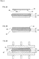
- the temporary fixing material 40 including saturated fatty acid as a main ingredient is applied on one surface of the copper circuit plate (the first member) 30 as shown in FIG. 2A .
- the saturated fatty acid with a carbon number 10 to 30 which is solid in room temperature (25°C) and easy to be phase transformed at comparatively low melting point. If the carbon number is smaller than 10, the handling property is not good because it is liquid in room temperature. If it is larger than 30, workability of applying on the copper circuit plate 30 is not good because the melting point is higher. Melting point of the saturated fatty acid having the carbon number 10 to 30 is about 32°C to 94°C, accordingly, the handling property is good since it is solid at room temperature and can be liquefied at comparatively low heating temperature.
- the saturated fatty acid having the carbon number 10 to 30 is, for example, capric acid of carbon number 10, lauric acid of carbon number 12, myristic acid of carbon number 14, palmitic acid of carbon number 16, stearic acid of carbon number 18, melissic acid of carbon number 30, or the like. These saturated fatty acids are inexpensive, so there is an advantage to be easy to obtain.
- An applying operation of the temporary fixing material 40 on the copper circuit plate 30 is, for example, performed by using a hot cylinder unit, though illustration thereof is omitted here.
- the temporary fixing material 40 is heated to be melted in the hot cylinder unit, and the melted temporary fixing material 40 is dropped on some points such as corner parts and the like at a surface of the copper circuit plate 30. Then, the temporary fixing material 40 dropped on the copper circuit plate 30 is cooled to room temperature and solidified, so that the copper circuit plate 30 to which the temporary fixing material 40 is adhered is formed.
- the copper circuit plate 30 is moved above the base table 91 by the stacking device 95 ( FIGS. 3A and 3B ) and stacked on the aluminum metal layer 22 of the ceramic substrate 20 arranged on the base table 91 in a positioned state ( FIG. 3C ).
- the applied temporary fixing material 40 is solidified.
- the temporary fixing material 40 can be melted by facing the adhering surface 30a of the copper circuit plate 30 to the rubber heater 96 and being heated.
- the copper circuit plate 30 is stacked on the ceramic substrate 20.
- the temporary fixing material 40 adhered to the copper circuit plate 30 is thinly extended to be layered, and closely adhered between the copper circuit plate 30 and the aluminum metal layer 22.
- the temporary fixing material 40 is cooled by being contact with the aluminum metal layer 22 which is not heated, and solidified.
- the laminated body 80 is obtained in a state in which the copper circuit plate 30 and the ceramic substrate 20 are precisely positioned and (temporarily) fixed.
- the temporary fixing material 40 can be solidified by natural cooling as described above; in addition, it is possible to solidify by actively cooling using the cooling device 98 as shown in FIG. 3C . In this case, it is possible to immediately fix the positioned state of the copper circuit plate 30 and the ceramic substrate 20. Accordingly, the workability can be further improved.
- the copper circuit plate 30 and the aluminum metal layer 22 of the ceramic substrate 20 are joined by solid-phase-diffusion joining in which copper and aluminum are diffused to each other, so that the power-module substrate 10 can be manufactured.
- the copper circuit plate 30 and the aluminum metal layer 22 of the ceramic substrate 20 are joined by holding them in vacuum atmosphere, at a load 0.3 MPa to 10 MPa, at heating temperature 400°C to 548°C, for 5 minutes to 240 minutes.
- the temporary fixing material 40 is decomposed and disappeared at an initial stage of this heating.
- the laminated body 80 in which the copper circuit plate (the first member) 30 and the ceramic substrate 20 are temporarily joined by the temporary fixing material 40 in the laminating step is formed beforehand in the joining step, the position shift between the copper circuit plate 30 and the ceramic substrate 20 can be prevented in the following joining step. Accordingly, it is possible to join the copper circuit plate 30 and the ceramic substrate 20 in the positioned state at a predetermined position precisely.
- the power-module substrate 10 can be efficiently manufactured, and the productivity can be improved.
- the temporary fixing material 40 is applied on the copper circuit plate 30 beforehand; and the copper circuit plate 40 is moved and stacked on the aluminum metal layer 22 of the ceramic substrate 20.
- the temporary fixing material 40 is applied on the aluminum metal layer 22 of the ceramic substrate 20 beforehand, and the copper circuit plate 30 is stacked thereon.
- the temporary fixing material 40 is melted by the heat of the copper circuit plate 30, so that the copper circuit plate 30 and the aluminum metal layer 22 can be closely adhered. Then, the temporary fixing material 40 is cooled by the aluminum metal layer 22 and solidified; and it is possible to fix the copper circuit plate 30 and the aluminum metal layer 22.
- the ceramic substrate 20 can be laminated on the copper circuit plate 30 by sucking the ceramic substrate 20 on which the temporary fixing material 40 is applied and moving it above the base table 91 on which the copper circuit plate 30 is arranged.
- the temporary fixing material 40 is dropped on the copper circuit plate 30 and then temporarily cooled to room temperature so as to be solidified; and then the temporary fixing material 40 is heated to be melted again when the copper circuit plate 30 is stacked on the ceramic substrate 20; so the copper circuit plate 30 and the ceramic substrate 20 are temporarily fixed.
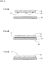
- FIG. 4 shows a second embodiment of the present invention
- FIG. 4C shows a power-module substrate (a joined body of the present invention) 11 manufactured by the present invention.
- This power-module substrate 11 is provided with an aluminum metal layer (a first member of the present invention) 32, and a ceramic plate (a second member of the present invention) 25 joined to this aluminum metal layer 32.
- the aluminum metal layer 32 and the ceramic plate 25 are formed to have a rectangular flat shape.
- a brazing foil is adhered by ultrasonic joining or the like, so as to form a joining-material layer 33 by this brazing foil beforehand.
- a temporary fixing material 41 including saturated fatty acid as a main ingredient is applied beforehand, as in the laminating step in the first embodiment.
- the melted temporary fixing material 41 is thinly extended to be layered between the ceramic substrate 2 and the joining-material layer 33 on the aluminum metal layer 32, so the ceramic plate 25 and the aluminum metal layer 32 are closely adhered.
- a laminated body 83 is formed in which the ceramic plate 25 and the aluminum metal layer 32 are temporarily joined (a laminating step).
- the ceramic plate 25 and the aluminum metal layer 32 are brazed by the joining-material layer 33 arranged therebetween, so that the power-module substrate 11 can be manufactured (a joining step).
- the temporary fixing material 41 is adhered to the surface of the joining-material layer 33 of the aluminum metal layer 32.
- the temporary fixing material 41 can be adhered to the surface of the ceramic plate 25.
- FIG. 5 shows a third embodiment of the present invention.
- FIG. 5C shows a heat sink equipped power-module substrate (a joined body of the present invention) 12 manufactured by the present invention.
- the heat sink equipped power-module substrate 12 is provided with a heat sink (a first member of the present invention) 51 and a power-module substrate (a second member of the present invention) 35 in which aluminum metal layers 37 and 38 are brazed on both surfaces of a ceramic plate 36; and manufactured by joining the one aluminum metal layer 38 of the power-module substrate 35 and the heat sink 51.
- the heat sink 51 is formed into a rectangular flat plate from pure aluminum having purity of 99.90% or higher or aluminum alloy (here, called merely "aluminum").
- a joining material layer 55 is formed beforehand on either one of the aluminum metal layer 38 of the power-module substrate 35 or the heat sink 51.
- the joining-material layer 55 can be employed a clad material which is formed to have three layers by laminating Al-Si-Mg based brazing material on both surfaces of an aluminum alloy plate of 3003 series, for example.
- the temporary fixing material 42 which is the same as the temporary fixing material 44 for joining material layer is applied beforehand on a surface of the heat sink 51 as well, and the power-module substrate 35 to which the joining-material layer 55 is adhered is stacked on the heat sink 51 in a state in which the temporary fixing material 42 is melted; so that the power-module substrate 35 and the heat sink 51 are closely adhered. Then, by cooling the temporary fixing material 42 in a state in which the power-module substrate 35 and the heat sink 51 are positioned, a laminated body 84 in which the power-module substrate 35 and the heat sink 51 are temporarily fixed is formed (a laminating step).
- this laminated body 84 (the power-module substrate 35 and the heat sink 51) under atmospheric pressure and in nitrogen atmosphere in a state of pressing in the stacking direction, the power-module substrate 35 and the heat sink 51 are brazed by the joining-material layer 55 therebetween, and the heat sink equipped power-module substrate 12 is manufactured (a joining step).
- FIG. 6 shows a fourth embodiment of the present invention.
- FIG. 6C shows a heat sink equipped power-module substrate (a joined body of the present invention) 13 manufactured by the present invention.
- the heat sink equipped power-module substrate 13 is provided with a heat sink (a first member of the present invention) 52 and a power-module substrate (a second member of the present invention) 45 in which aluminum metal layers 47 and 48 are brazed on both surfaces of a ceramic plate 46, and manufactured by joining the one aluminum metal layer 48 of the power-module substrate 45 and the heat sink 52.
- the heat sink 52 is formed into a rectangular flat shape from pure copper or copper alloy (here, called merely "copper").
- the aluminum metal layer 48 of the power-module substrate 45 and the heat sink 52 are joined by solid-phase diffusion joining in which copper and aluminum are diffused to each other, so that the heat sink equipped power-module substrate 13 is manufactured (a joining step).
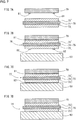
- FIG. 7 shows a fifth embodiment of the present invention
- FIG. 7D shows a heat sink equipped power-module substrate (a multilayer joined body of the present invention) 14 manufactured by the present invention.
- the heat sink equipped power-module substrate 14 is provided with a copper circuit plate (a first member of the present invention) 70, a ceramic substrate (a second member of the present invention) 75 in which aluminum metal layers 72 and 73 are laminated on both surfaces of a ceramic plate 71, and a heat sink (a third member of the present invention) 53.
- the heat sink equipped power-module substrate 14 is manufactured by joining the one aluminum metal layer 72 of the ceramic substrate 75 and the copper circuit plate 70 and joining the other aluminum metal layer 73 and the heat sink 53.
- the heat sink 53 is made from pure copper or copper alloy (here, called merely as "copper”) into a rectangular flat plate.
- a temporary fixing material 81 including saturated fatty acid as a main ingredient is applied on the copper circuit plate 70 beforehand, and the ceramic substrate 75 is stacked thereon in a state in which the temporary fixing material 81 is melted; so that the ceramic substrate 75 and the copper circuit plate 70 are closely adhered with the temporary fixing material 81 therebetween. Then, by cooling the temporary fixing material 81 in a state in which the ceramic substrate 75 and the copper circuit plate 70 are positioned, a laminated body 76 in which the ceramic substrate 75 and the copper circuit plate 70 are temporarily fixed by the temporary fixing material 81 is formed (a laminating step).
- the temporary fixing material 81 can be adhered also on a surface of the ceramic substrate 75 (the aluminum metal layer 72) other than the copper circuit plate 70.
- the laminated body 76 which is formed in the laminating step by temporarily fixing the ceramic substrate 75 and the copper circuit plate 70, is temporarily fixed on the heat sink (the third member of the present invention) 53 by a second temporary fixing material 82 including saturated fatty acid as a main ingredient and having lower melting point than that of the temporary fixing material 81 (a second laminating step).
- the temporary fixing material 81 includes stearic acid (a carbon number 18, melting point about 70°C) as a main ingredient
- lauric acid a carbon number 12, melting point about 44°C
- the second temporary fixing material 82 is applied beforehand on the aluminum metal layer 73 of the laminated body 76, and the second temporary fixing material 82 is melted at lower temperature than the melting temperature of the temporary fixing material 81; then the laminated body 76 and the heat sink 53 are stacked with positioning, so that the laminated body 76 and the heat sink 53 are closely adhered by the second temporary fixing material 82 therebetween. Subsequently, by cooling the second temporary fixing material 82, the laminated body 76 and the heat sink 53 are fixed by the second temporary fixing material 82, so that a second laminated body 77 in which the laminated body 76 and the heat sink 53 are temporarily fixed is formed (a second laminating step).
- the second temporary fixing material 82 can be adhered on a surface of the heat sink 53 other than the aluminum metal layer 73 of the laminated body 76.
- the temporary fixing material 81 since using the second temporary fixing material 82 having lower melting point than the melting point of the temporary fixing material 81 which temporarily fixes the copper circuit plate 70 and the ceramic substrate 75, the temporary fixing material 81 is not melted, and the heat sink 53 can be temporarily fixed in a state in which the copper circuit plate 70 and the ceramic substrate 75 are fixed.
- the laminated body 76 and the heat sink 53 in which the copper circuit plate 70 and the ceramic substrate 75 are stacked can be temporarily fixed without shifting the position between the copper circuit plate 70 and the ceramic substrate 75. Accordingly, three members, the copper circuit plate 70, the ceramic substrate 75, and the heat sink 53 can be fixed with an accurate position.
- the second laminated body which is formed by temporarily fixing the copper circuit plate 70, the ceramic substrate 75 and the heat sink 53 is pressed in the stacking direction and heated at lower temperature than the eutectic temperature of copper and aluminum; as a result, they can be joined by solid-phase-diffusion joining by diffusing copper and aluminum to each other (a joining step).
- the copper circuit plate 70, the ceramic substrate 75, and the heat sink 53 can be concurrently joined by the heat sink equipped power-module substrate manufacturing method according to the fifth embodiment, so that the heat sink equipped power-module substrate 14 can be efficiently manufactured.
- the heat sink equipped power-module substrate 14 is manufactured by joining the one aluminum metal layer 72 of the ceramic substrate 75 and the copper circuit plate 70, and joining the other aluminum metal layer 73 and the copper-made heat sink 53 by the solid-phase-diffusion joining between copper and aluminum; however, it is acceptable that an aluminum circuit plate is joined on the aluminum metal layer 72 of the ceramic substrate 73 and an aluminum-made heat sink is joined on the aluminum metal layer 73.
- joining material layers are respectively formed beforehand, and these members are stacked and temporarily fixed with the respective joining material layers therebetween.
- a clad material which is formed to have three layers by laminating Al-Si-Mg based brazing material on both surfaces of an aluminum alloy plate of 3003 series can be employed.
- laminated body were formed by dropping temporary fixing materials shown in Table 1 on rectangle copper plates of 30 mm ⁇ 30 mm, thickness 1.0 mm, and stacking and temporarily fixing rectangle aluminum plates of 25 mm ⁇ 25 mm, thickness 0.6 mm thereon. Modeling a moving state of the laminated bodies, the copper plates of the laminated bodies were shaken horizontally at a speed about 30 mm/s; and confirming position shift of the aluminum plates by looking, bondability of the laminated bodies which were temporarily fixed were evaluated. If the position shift was not larger than 1 mm, it was evaluated as "excellent”. If the position shift was larger than 1 mm and smaller than 10 mm, it was evaluated as "good”. If the position shift was not smaller than 10 mm, it was evaluated as "bad".
- Joined bodies were formed from the laminated bodies by pressing in the stacking direction at 1.0 MPa in vacuum atmosphere and heating at 540°C for 60 minutes.
- modeling a usage state of the joined bodies, in an initial state after joining and a state after 3000 times of thermal cycling between -40°C and 100°C existence of unjoined parts at joining surfaces between the copper plate and the aluminum plate were observed by an ultrasonic image measuring device. If there was not an unjoined part larger than 2% in the joining surfaces, it was evaluated as "excellent”. If there was an unjoined part not smaller than 5% or a void in which a diameter thereof is not smaller than 2 mm, it was evaluated as (bad).
- EXCELLENT EXCELLENT Invention 4 Myristic Acid : CH 3 - (CH 2 ) 12 - COOH approx. 54°C EXCELLENT EXCELLENT Invention: 5 Palmitic Acid : CH 3 - (CH 2 ) 14 - COOH approx. 63°C EXCELLENT EXCELLENT Invention: 6 Stearic Acid : CH 3 - (CH 2 ) 16 - COOH approx. 70°C EXCELLENT EXCELLENT Invention: 7 Melissic Acid: CH 3 - (CH 2 ) 28 - COOH approx. 94°C EXCELLENT EXCELLENT
- the present invention may be applied when the first member made from a metal plate and the second member made from a metal plate or a ceramic plate are joined.
- the present invention may be applied to a case of manufacturing a joined body of the first member and the second member used for the other purpose than a power module, and further may include a case of joining laminated bodies of these without both pressing and heating.
- the joined body is manufactured from the first member and the second member in a relation of one-to-one in the above embodiments, it is not limited to this.
- the present invention may be applied to cases of manufacturing various laminated bodies and joined bodies: for example, in a case in which two or more first members are joined to one second member.
- the positions of the joining surfaces of the members can be prevented from shifting when joining the metal plates to each other or joining the metal plate and the ceramic plate: so that the joined body of these can be efficiently manufactured.
Landscapes
- Chemical & Material Sciences (AREA)
- Engineering & Computer Science (AREA)
- Ceramic Engineering (AREA)
- Materials Engineering (AREA)
- Structural Engineering (AREA)
- Organic Chemistry (AREA)
- Manufacturing & Machinery (AREA)
- Inorganic Chemistry (AREA)
- Cooling Or The Like Of Semiconductors Or Solid State Devices (AREA)
- Ceramic Products (AREA)
Abstract
Description
- The present invention relates to a manufacturing method of a laminated body structured from a number of members used for manufacturing a power-module substrate of a semiconductor device controlling large electric current and high voltage, a manufacturing method of a power-module substrate, and a manufacturing device of a laminated body.
- Priority is claimed on Japanese Patent Application No.
2014-136646 filed July 2, 2014 2014-235949 filed November 20, 2014 2015-130973 filed June 30, 2015 - Conventionally, as a power-module substrate, it is known that a circuit plate is joined on one surface of a ceramic substrate in a laminated state and a heat-radiation plate is joined on another surface of the ceramic substrate in a laminated state. This power-module substrate is formed into a power module by soldering electric elements such as a semiconductor chip (a power element) or the like on the circuit plate and joining a heat sink on the heat-radiation plate.
- Methods of joining metal plates to be the circuit plate and the heat-radiation plate on the ceramic substrate in the laminated state for this power-module substrate are described in Patent Documents 1 and 2 for example.
- Patent Document 1 discloses a manufacturing method of a power-module substrate having an insulating layer and a circuit layer formed on one surface of the insulating layer. This manufacturing method of power-module substrate has a circuit layer forming process in which the circuit layer is formed by laminating a copper layer on the aluminum layer after arranging an aluminum layer on the one surface of the insulating layer, so that the aluminum layer and the copper layer are solid-phase-diffusion joined by weighting and holding a heating state.
- In Patent Document 2, a brazing foil is laminated on one surface of a metal flat plate with a resin-coating layer (including octanediol as organic resin) therebetween beforehand, this stacked body of the metal flat plate and the brazing foil is punched out and formed to have an outer shape of a circuit layer, and the brazing foil which is stacked on the circuit layer is stacked on a ceramic flat plate: so that the circuit layer and the ceramic flat plate are stacked and joined with the brazing foil.
-
- Patent Document 1 Japanese Unexamined Patent Application, First Publication No.
2013-229545 - Patent Document 2 Japanese Unexamined Patent Application, First Publication No.
2010-10561 - According to the manufacturing method of a power-module substrate described in Patent Document 1, the copper layer is stacked after joining the aluminum layer on the insulating layer. However, if merely stacking the aluminum layer and the copper layer directly, these metal members are slipped sideways and a position shift is easy to be occurred (a sideways slip) when installing in a pressurizing tool or pressurizing. Furthermore, if using octanediol as the method described in Patent Document 2, since octanediol is liquid at room temperature, there is a case of slipping sideways because adhesion is not enough. Moreover, problems of the sideways slip between the members may be occurred when stacking the power-module substrate and the heat sink (i.e., laminating metal members) or stacking the metal member and the insulating layer such as the ceramic substrate or the like.
- Deterioration of precision of a laminating position owing to the sideways slip between the members causes deterioration of heat radiation property (increase of thermal resistance). Accordingly, it is desired to prevent the position shift.
- The present invention is achieved in consideration of the above circumstances, and has an object to provide a joined body manufacturing method that, when joining the metal plates to each other or the metal plate to the ceramic plate, can efficiently manufacture the joined body with preventing the position shift between joining surfaces of each member, and to provide a power-module substrate manufacturing method in which the joined body manufacturing method is applied to a power-module substrate.
- The present invention has a laminating step forming a laminated body: by coating temporary fixing material including saturated fatty acid as a main ingredient on either a first member made of a metal plate or a second member including one or more of metal plates or ceramic plates; stacking and positioning the first member and the second member with the temporary fixing material therebetween in a state in which the temporary fixing material is melted; and cooling the temporary fixing material to form the laminated body in which the stacked first member and the second member are temporarily joined; and a joining step forming a joined body in which the first member and the second member are joined by heating with pressurizing the laminated body in a stacking direction.
- In this manufacturing method, since the first member and the second member are temporarily joined by the temporary fixing material including the saturated fatty acid as the main ingredient, the first member and the second member are not shifted but held in a state in which they are positioned in the joining step after that. Accordingly, subsequent handling is easy, so that it is possible to improve productivity and join the members in an accurately positioned state.
- The temporary fixing material, using the saturate fatty acid which is solid in room temperature, is melted by heating and liquefied. Therefore, after laminating the first member and the second member, the first member and the second member can be easily joined by cooling the temporary fixing material to room temperature so as to be solidified. In the joining step, the saturated fatty acid does not influence joining surfaces between the first and second members because the saturated fatty acid is rapidly decomposed at sufficiently lower temperature than joining temperature.
- Moreover, the saturated fatty acid has high fluidity in a liquefied melted state and can be spread between the stacked first and second members, so that it is possible to maintain good bondability in a closely adhering state.
- Accordingly, it is possible to prevent position shift between the joining surfaces of the members when the first member and the second member which are the metal plates or structured from the metal plate and the ceramic plate and the like are joined, so that the joined body of these can be manufactured efficiently.
- In the joined body manufacturing method according to the present invention, it is preferable that a carbon number of the saturated fatty acid of the temporary fixing material be 10 to 30.
- If the carbon number is smaller than 10, the handling property is not good because it is liquid in room temperature. If it exceeds 30, workability of applying on the first member or the second member is not good because the melting point is high. Melting point of the saturated fatty acid having the
carbon number 10 to 30 is about 32°C to 94°C: accordingly, the handling property is good since it is solid at room temperature and can be liquefied at comparatively low heating temperature. - The saturated fatty acid having the
carbon number 10 to 30 is, for example, capric acid ofcarbon number 10, lauric acid ofcarbon number 12, myristic acid ofcarbon number 14, palmitic acid of carbon number 16, stearic acid of carbon number 18, melissic acid ofcarbon number 30, and the like. These saturated fatty acids are inexpensive, so there is an advantage of easiness to obtain. - In the joined body manufacturing method according to the present invention, it is preferable that a joining-material layer be formed on either one surface of the first member or the second member, and the first member and the second member be laminated with the joining-material layer and the temporary fixing material therebetween in the laminating step.
- A multilayer joined body manufacturing method according to the present invention applying the above-mentioned joined body manufacturing method includes a second laminating step before the joining step temporarily joining a third member made of a metal plate on the laminated body formed by the laminating step, and in the second laminating step, a second laminated body in which the laminated body and the third member are temporarily joined is formed: by applying a second temporary fixing material including saturated fatty acid with a lower melting point than the temporary fixing material as a main ingredient, on either one of the laminated body or the third body beforehand; melting the second temporary fixing material at lower temperature than melting temperature of the temporary fixing material when stacking the laminated body and the third member; and cooling the second temporary fixing material after positioning and stacking the laminated body and the third body, and in the joining step, by pressurizing and heating the second laminated body in a stacking direction thereof, the multilayer joined body in which the third member is further joined on the joined body in which the first member and the second member are joined.
- Also in the multilayer joined body manufacturing method according to the present invention, it is preferable that a carbon number of the saturated fatty acid of the temporary fixing material be 10 to 30. Moreover, it is preferable that a joining-material layer be formed on either one surface of the first member or the second member, and the first member and the second member be stacked with the joining-material layer and the temporary fixing material therebetween in the laminating step. Furthermore, it is preferable that a second joining-material layer be formed on either one surface of the second laminated body or the third member, and the laminated body and the third member be stacked with the second temporary fixing material and the second joining-material layer therebetween in the second laminating step.
- A heat sink equipped power-module substrate manufacturing method according to the present invention is a heat sink equipped power-module substrate manufacturing method applying the above-mentioned multilayer joined body manufacturing method, in which the first member is a circuit plate made of copper or aluminum, the second member is a ceramic substrate made by laminating aluminum metal layers on both surfaces of a ceramic plate, the third member is a heat sink made of copper or aluminum, and in the joining step, the heat sink equipped power-module substrate is formed as the multilayer joined body by joining the first member and one of the aluminum metal layers of the second member and joining the third member and the other of the aluminum metal layers of the second member.
- A power-module substrate manufacturing method according to the present invention is a power-module substrate manufacturing method applying the above-mentioned joined body manufacturing method, in which the first member is a copper circuit plate, the second member is a ceramic substrate made by laminating aluminum metal layers on both surfaces of a ceramic plate, and in the joining step, the power-module substrate is formed as the joined body by joining the first member and one of the aluminum metal layers of the second member.
- A heat sink equipped power-module substrate manufacturing method according to the present invention is a heat sink equipped power-module substrate manufacturing method applying the above-mentioned joined body manufacturing method, in which the first member is a heat sink made of copper or aluminum, the second member is a power-module substrate formed by laminating metal layers on both surfaces of a ceramic plate, and in the joining step, the heat sink equipped power-module substrate is formed as the joined body by joining the first member and one of the metal layers of the second member.
- In this heat sink equipped power-module substrate manufacturing method, it is preferable that the joining-material layer be temporary joined on either one surface of the first member or the second member by temporary fixing material for joining-material layer before the laminating step, and in the laminating step, the temporary fixing material be applied on either one of the first member or the second member on which the joining-material layer is not formed.
- A laminated body manufacturing device according to the present invention is a laminated body manufacturing device temporarily-joining a first member made of a metal plate and a second member including one or more of metal plates or ceramic plates in a stacked state with temporary fixing material including saturated fatty acid as a main ingredient therebetween, in which the temporary fixing material is formed on either one of the first member or the second member, and the manufacturing device includes a stacking device stacking the first member and the second member by moving one on which the temporary fixing material is formed onto the other on which the temporary fixing material is not formed, and a heating device melting the temporary fixing material when the first member and the second member are laminated.
- The temporary fixing material using the saturated fatty acid which is solid in room temperature is melted by heating; so it is necessary to be heated when the first member and the second member are laminated. Accordingly, by providing the heating device heating the temporary fixing material when laminating the first member and the second member, the first member and the second member can be fixed efficiently.
- A laminated body manufacturing device according to the present invention is a laminated body manufacturing device temporarily-joining a first member made of a metal plate and a second member including one or more of metal plates or ceramic plates in a laminated state with temporary fixing material including saturated fatty acid as a main ingredient therebetween, wherein the temporary fixing material is formed on either one of the first member or the second member, including a stacking device stacking the first member and the second member by moving the other on which the temporary fixing material is not formed onto the one on which the temporary fixing material is formed, and a heating device melting the temporary fixing material when the first member and the second member are laminated.
- The saturated fatty acid which is the main ingredient of the temporary fixing material has high fluidity in a liquefied melted state. Accordingly, when moving the one plate in which the temporary fixing material is formed, it is desired that the temporary fixing material is solid just before stacking both the members in order to prevent the melted temporary fixing material from sticking to an unnecessary part other than a joining part. Therefore, in the joined body manufacturing device of the present invention, the one plate on which the temporary fixing material is formed is not moved but the other plate is moved; so that the one plate on which the temporary fixing material is formed can be maintained in a stationary state. As a result, it is possible to prevent the temporary fixing material from sticking to the unnecessary part. Accordingly, it is possible to efficiently fix the first member and the second member.
- In the laminated body manufacturing device according to the present invention, it is preferable to provide a cooling device which cools the temporary fixing material after laminating the first member and the second member.
- By solidifying the melted temporary fixing material by natural cooling, the first member and the second member can be joined. By positively cooling it using the cooling device, it is possible to fix instantly a state in which the first member and the second member are positioned.
- According to the present invention, when joining the metal plates to each other and joining the metal plate and the ceramic plate, the position shift at the joining surfaces between the members can be prevented, so that the joined body of these can be manufactured efficiently.
-
-
FIG. 1 is a sectional view showing a power-module substrate manufactured in a first embodiment of the present invention. -
FIG. 2 is a sectional view schematically showing steps of producing the power-module substrate inFIG. 1 . -
FIG. 3 is a schematic view explaining a layered body manufacturing device according to the present invention. -
FIG. 4 is a schematic view explaining a manufacturing method of a second embodiment of the present invention. -
FIG 5 is a schematic view explaining a manufacturing method of a third embodiment of the present invention. -
FIG. 6 is a schematic view explaining a manufacturing method of a fourth embodiment of the present invention. -
FIG. 7 is a schematic view explaining a manufacturing method of a fifth embodiment of the present invention. - Below, embodiments of the present invention will be explained.
-
FIG. 1 shows a power-module substrate 10 manufactured in a first embodiment of the present invention. - This power-module substrate (a joined body of the present invention) 10 is provided with a copper circuit plate (a first member of the present invention) 30 and a ceramic substrate (a second member of the present invention) 20 in which aluminum metal layers 22 and 23 are laminated on both surfaces of a
ceramic plate 21; and the one aluminum-metal plate 22 of theceramic substrate 20 and thecopper circuit plate 30 are joined. In this case, theceramic plate 21 of theceramic substrate 20, the aluminum metal layers 22 and 23 and thecopper circuit plate 30 are formed as a rectangular flat shape. - An
electric member 60 such as a semiconductor chip or the like is soldered on a surface of thecopper circuit plate 30, and aheat sink 50 is joined on thealuminum metal layer 23 arranged at a counter side to thecopper circuit layer 30, so that the power-module substrate 10 is formed as a power module. - The
ceramic plate 21 is made into a rectangular shape from nitride ceramics such as AlN (aluminum nitride), Si3N4 (silicon nitride) or the like, or oxide ceramics such as Al2O3 (alumina) or the like as main ingredient, for example. Thickness of theceramic plate 21 is 0.125 mm to 1.0 mm. - The aluminum metal layers 22 and 23 are formed usually into a rectangular flat plate smaller than the
ceramic plate 21 with thickness 0.1 mm to 3.0 mm, from pure aluminum with purity of 99.90% or higher or aluminum alloy (here, called merely "aluminum"). The aluminum metal layers 22 and 23 are joined on theceramic plate 21 by brazing material of Al-Si based, Al-Ge based, Al-Cu based, Al-Mg based, or Al-Mn based or the like, which is used as joining material. - The
copper circuit plate 30 is made of pure copper such as oxygen-free copper, tough-pitch copper or the like, or copper alloy (here, called merely "copper" in the present invention). Thickness of thecopper circuit plate 30 is 0.1 mm to 5.0 mm. Thecopper circuit layer 30 is joined on thealuminum metal layer 22 of theceramic substrate 20 by solid-phase-diffusion joining as stated below. - Next, a laminated body manufacturing device 90 (refer to
FIG. 3 ) for producing the power-module substrate 10 which is structured as above will be explained. - The laminated
body manufacturing device 90 manufactures alaminated body 80 in which the copper circuit plate (the first member of the present invention) 30 on whichtemporary fixing material 40 including saturated fatty acid as main ingredient is formed is temporarily joined on thealuminum metal layer 22 of the ceramic substrate (the second member of the present invention) 20. - The laminated
body manufacturing device 90 of the present embodiment is provided with, as shown inFIG. 3 , a base table 91 on which theceramic substrate 20 is arranged, a stackingdevice 95 moving thecopper circuit plate 30 on which thetemporary fixing material 40 is formed onto theceramic substrate 20 which is arranged on the base table 91 and stacking thecopper circuit plate 30 and theceramic substrate 20 with positioning theceramic substrate 20, and aheating device 96 melting thetemporary fixing material 40 when laminating thecopper circuit plate 30 and theceramic substrate 20. - In the base table 91, as shown in
FIG. 3B and FIG. 3C , guide pins 92 are provided to stand on an arranging surface of theceramic substrate 20 with intervals surrounding side surfaces of theceramic substrate 20. By arranging theceramic substrate 20 in an area surrounded by these guide pins 92, theceramic substrate 20 is positioned on the base table 91. - The stacking
device 95, as shown inFIG. 3A and FIG. 3B , can be structured by a cylinder unit for picking up and stacking which is installed so as to move along xyz directions, for example. The stackingdevice 95 stacks thecopper circuit plate 30 and theceramic substrate 20 by moving thecopper circuit plate 30 in a state in which an adheringsurface 30a is downward to above the base table 91 on which theceramic substrate 20 is arranged, and stacks the adheringsurface 30a of thecopper circuit plate 30 on theceramic substrate 20 on the base table 91. Specifically, as shown inFIG. 3A to FIG. 3C , thecopper circuit plate 30 is moved by air-suction at an upper surface which is opposite to the adheringsurface 30a of thecopper circuit plate 30 by the stackingdevice 95. - The
heating device 96 may be structured by a rubber heater, as shown inFIG. 3A for example. Thetemporary fixing material 40 on the adheringsurface 30a can be heated and melted by arranging the adheringsurface 30a of thecopper circuit plate 30 to be opposite to the rubber heater (the heating device) 96. - The stacking
device 95 is provided with atemperature measuring device 97 for observing the melted state of thetemporary fixing material 40 when thecopper circuit plate 30 is moved. By measuring the temperature of thecopper circuit plate 30 using thetemperature measuring device 97, it is possible to confirm the melted states of thetemporary fixing material 40 when heating thecopper circuit plate 30 by theheating device 96, and before and after stacking thecopper circuit plate 30 and theceramic substrate 20. As thetemperature measuring device 97, an infrared thermometer can be used, for example. In the present embodiment, thetemperature measuring device 97 measures the temperature of thecopper circuit plate 30 held by the stackingdevice 95. - The laminated
body manufacturing device 90 is provided with acooling device 98 for cooling thecopper circuit plate 30 and theceramic substrate 20 after stacking. Thecooling device 98 is provided at the stackingdevice 95, and may be structured by a cooling nozzle blowing air as shown inFIG. 3C for example. - Next, a method of forming the
laminated body 80 and producing the power-module substrate 10 using the above-mentioned laminatedbody manufacturing device 90 will be explained. - First, the
temporary fixing material 40 including saturated fatty acid as a main ingredient is applied on one surface of the copper circuit plate (the first member) 30 as shown inFIG. 2A . For thistemporary fixing material 40, preferably used is the saturated fatty acid with acarbon number 10 to 30 which is solid in room temperature (25°C) and easy to be phase transformed at comparatively low melting point. If the carbon number is smaller than 10, the handling property is not good because it is liquid in room temperature. If it is larger than 30, workability of applying on thecopper circuit plate 30 is not good because the melting point is higher. Melting point of the saturated fatty acid having thecarbon number 10 to 30 is about 32°C to 94°C, accordingly, the handling property is good since it is solid at room temperature and can be liquefied at comparatively low heating temperature. - The saturated fatty acid having the
carbon number 10 to 30 is, for example, capric acid ofcarbon number 10, lauric acid ofcarbon number 12, myristic acid ofcarbon number 14, palmitic acid of carbon number 16, stearic acid of carbon number 18, melissic acid ofcarbon number 30, or the like. These saturated fatty acids are inexpensive, so there is an advantage to be easy to obtain. - An applying operation of the
temporary fixing material 40 on thecopper circuit plate 30 is, for example, performed by using a hot cylinder unit, though illustration thereof is omitted here. Thetemporary fixing material 40 is heated to be melted in the hot cylinder unit, and the meltedtemporary fixing material 40 is dropped on some points such as corner parts and the like at a surface of thecopper circuit plate 30. Then, thetemporary fixing material 40 dropped on thecopper circuit plate 30 is cooled to room temperature and solidified, so that thecopper circuit plate 30 to which thetemporary fixing material 40 is adhered is formed. - Next, as shown in
FIG. 2B , stacking thecopper circuit plate 30 on which thetemporary fixing material 40 is adhered beforehand and thealuminum metal layer 22 of theceramic substrate 20, thecopper circuit plate 30 and theceramic substrate 20 are temporarily joined by thetemporary fixing material 40. - The
copper circuit plate 30 is moved above the base table 91 by the stacking device 95 (FIGS. 3A and 3B ) and stacked on thealuminum metal layer 22 of theceramic substrate 20 arranged on the base table 91 in a positioned state (FIG. 3C ). - When the
copper circuit plate 30 is moved, the appliedtemporary fixing material 40 is solidified. In the middle of a moving route of thecopper circuit plate 30 by the stackingdevice 95, thetemporary fixing material 40 can be melted by facing the adheringsurface 30a of thecopper circuit plate 30 to therubber heater 96 and being heated. - Then, in a state in which the
temporary fixing material 40 is melted, as shown inFIG. 2B andFIG. 3C , thecopper circuit plate 30 is stacked on theceramic substrate 20. At this time, by stacking on theceramic substrate 20, thetemporary fixing material 40 adhered to thecopper circuit plate 30 is thinly extended to be layered, and closely adhered between thecopper circuit plate 30 and thealuminum metal layer 22. Then, thetemporary fixing material 40 is cooled by being contact with thealuminum metal layer 22 which is not heated, and solidified. As a result, thelaminated body 80 is obtained in a state in which thecopper circuit plate 30 and theceramic substrate 20 are precisely positioned and (temporarily) fixed. - The
temporary fixing material 40 can be solidified by natural cooling as described above; in addition, it is possible to solidify by actively cooling using thecooling device 98 as shown inFIG. 3C . In this case, it is possible to immediately fix the positioned state of thecopper circuit plate 30 and theceramic substrate 20. Accordingly, the workability can be further improved. - Then, as shown in
FIG. 2C , by pressing thelaminated body 80 in which thecopper circuit plate 30 and theceramic substrate 20 are temporarily joined in the stacking direction and heating it at a lower temperature than eutectic temperature of copper and aluminum, thecopper circuit plate 30 and thealuminum metal layer 22 of theceramic substrate 20 are joined by solid-phase-diffusion joining in which copper and aluminum are diffused to each other, so that the power-module substrate 10 can be manufactured. Specifically thecopper circuit plate 30 and thealuminum metal layer 22 of theceramic substrate 20 are joined by holding them in vacuum atmosphere, at a load 0.3 MPa to 10 MPa, at heating temperature 400°C to 548°C, for 5 minutes to 240 minutes. Thetemporary fixing material 40 is decomposed and disappeared at an initial stage of this heating. - As described above, in the power-module substrate manufacturing method of the present embodiment, since the
laminated body 80 in which the copper circuit plate (the first member) 30 and theceramic substrate 20 are temporarily joined by thetemporary fixing material 40 in the laminating step is formed beforehand in the joining step, the position shift between thecopper circuit plate 30 and theceramic substrate 20 can be prevented in the following joining step. Accordingly, it is possible to join thecopper circuit plate 30 and theceramic substrate 20 in the positioned state at a predetermined position precisely. - Therefore, the power-
module substrate 10 can be efficiently manufactured, and the productivity can be improved. - In the above-mentioned first embodiment, the
temporary fixing material 40 is applied on thecopper circuit plate 30 beforehand; and thecopper circuit plate 40 is moved and stacked on thealuminum metal layer 22 of theceramic substrate 20. However, it is permitted that thetemporary fixing material 40 is applied on thealuminum metal layer 22 of theceramic substrate 20 beforehand, and thecopper circuit plate 30 is stacked thereon. - In this case, by stacking the heated
copper circuit plate 30 on thealuminum metal layer 22 on which thetemporary fixing material 40 is applied, thetemporary fixing material 40 is melted by the heat of thecopper circuit plate 30, so that thecopper circuit plate 30 and thealuminum metal layer 22 can be closely adhered. Then, thetemporary fixing material 40 is cooled by thealuminum metal layer 22 and solidified; and it is possible to fix thecopper circuit plate 30 and thealuminum metal layer 22. - In this case, instead of the
ceramic substrate 20 on which thetemporary fixing material 40 is formed, but the thecopper circuit plate 30 is moved; accordingly, theceramic substrate 20 on which thetemporary fixing material 40 is formed is in a stationary state. Therefore, the meltedtemporary fixing material 40 is prevented from adhering to an unnecessary part other than joining parts; and thecopper circuit plate 30 and theceramic substrate 20 are efficiently fixed. - In addition, the
ceramic substrate 20 can be laminated on thecopper circuit plate 30 by sucking theceramic substrate 20 on which thetemporary fixing material 40 is applied and moving it above the base table 91 on which thecopper circuit plate 30 is arranged. - In the first embodiment, the
temporary fixing material 40 is dropped on thecopper circuit plate 30 and then temporarily cooled to room temperature so as to be solidified; and then thetemporary fixing material 40 is heated to be melted again when thecopper circuit plate 30 is stacked on theceramic substrate 20; so thecopper circuit plate 30 and theceramic substrate 20 are temporarily fixed. In addition, it is possible to adhere by stacking thecopper circuit plate 30 and theceramic substrate 20 before the dropped temporary fixing material is cooled. -
FIG. 4 shows a second embodiment of the present invention; andFIG. 4C shows a power-module substrate (a joined body of the present invention) 11 manufactured by the present invention. This power-module substrate 11 is provided with an aluminum metal layer (a first member of the present invention) 32, and a ceramic plate (a second member of the present invention) 25 joined to thisaluminum metal layer 32. In this case, thealuminum metal layer 32 and theceramic plate 25 are formed to have a rectangular flat shape. - In order to manufacture the power-module substrate 11 structured as above, on one surface of the
aluminum metal layer 32, as shown inFIG. 4A , a brazing foil is adhered by ultrasonic joining or the like, so as to form a joining-material layer 33 by this brazing foil beforehand. On a surface of the joining-material layer 33, atemporary fixing material 41 including saturated fatty acid as a main ingredient is applied beforehand, as in the laminating step in the first embodiment. Then, by stacking thealuminum metal layer 32 and theceramic plate 25 with the joining-material layer 33 therebetween in a state in which thetemporary fixing material 41 is melted, the meltedtemporary fixing material 41 is thinly extended to be layered between the ceramic substrate 2 and the joining-material layer 33 on thealuminum metal layer 32, so theceramic plate 25 and thealuminum metal layer 32 are closely adhered. Subsequently, by cooling thetemporary fixing material 41 in a state in which theceramic plate 25 and thealuminum metal layer 32 are positioned, alaminated body 83 is formed in which theceramic plate 25 and thealuminum metal layer 32 are temporarily joined (a laminating step). - Similarly to the first embodiment, by pressing the laminated body of the
ceramic plate 25 and thealuminum metal layer 32 in the stacking direction and heating them in vacuum, theceramic plate 25 and thealuminum metal layer 32 are brazed by the joining-material layer 33 arranged therebetween, so that the power-module substrate 11 can be manufactured (a joining step). - In the second embodiment, the
temporary fixing material 41 is adhered to the surface of the joining-material layer 33 of thealuminum metal layer 32. However, thetemporary fixing material 41 can be adhered to the surface of theceramic plate 25. -
FIG. 5 shows a third embodiment of the present invention.FIG. 5C shows a heat sink equipped power-module substrate (a joined body of the present invention) 12 manufactured by the present invention. The heat sink equipped power-module substrate 12 is provided with a heat sink (a first member of the present invention) 51 and a power-module substrate (a second member of the present invention) 35 in which aluminum metal layers 37 and 38 are brazed on both surfaces of a ceramic plate 36; and manufactured by joining the onealuminum metal layer 38 of the power-module substrate 35 and theheat sink 51. Theheat sink 51 is formed into a rectangular flat plate from pure aluminum having purity of 99.90% or higher or aluminum alloy (here, called merely "aluminum"). - In order to manufacture the heat sink equipped power-
module substrate 12 structure as above, a joiningmaterial layer 55 is formed beforehand on either one of thealuminum metal layer 38 of the power-module substrate 35 or theheat sink 51. As the joining-material layer 55, can be employed a clad material which is formed to have three layers by laminating Al-Si-Mg based brazing material on both surfaces of an aluminum alloy plate of 3003 series, for example. - As shown in
FIG. 5A , on a surface of thealuminum metal layer 38,temporary fixing material 44 for joining material layer including saturated fatty acid as a main ingredient is applied beforehand; and the joining-material layer 55 is stacked in a state in which thetemporary fixing material 44 for joining-material layer is melted, so that thealuminum metal layer 38 and the joining-material layer 55 are closely adhered by thetemporary fixing material 44 for joining-material layer therebetween. Then, by cooling thetemporary fixing material 44 for joining-material layer in a state in which thealuminum metal layer 38 and the joining-material layer 55 are positioned, thealuminum metal layer 38 and the joining-material layer 55 are joined (temporarily fixed). - Furthermore, the
temporary fixing material 42 which is the same as thetemporary fixing material 44 for joining material layer is applied beforehand on a surface of theheat sink 51 as well, and the power-module substrate 35 to which the joining-material layer 55 is adhered is stacked on theheat sink 51 in a state in which thetemporary fixing material 42 is melted; so that the power-module substrate 35 and theheat sink 51 are closely adhered. Then, by cooling thetemporary fixing material 42 in a state in which the power-module substrate 35 and theheat sink 51 are positioned, alaminated body 84 in which the power-module substrate 35 and theheat sink 51 are temporarily fixed is formed (a laminating step). - By heating this laminated body 84 (the power-module substrate 35 and the heat sink 51) under atmospheric pressure and in nitrogen atmosphere in a state of pressing in the stacking direction, the power-module substrate 35 and the
heat sink 51 are brazed by the joining-material layer 55 therebetween, and the heat sink equipped power-module substrate 12 is manufactured (a joining step). -
FIG. 6 shows a fourth embodiment of the present invention.FIG. 6C shows a heat sink equipped power-module substrate (a joined body of the present invention) 13 manufactured by the present invention. The heat sink equipped power-module substrate 13 is provided with a heat sink (a first member of the present invention) 52 and a power-module substrate (a second member of the present invention) 45 in which aluminum metal layers 47 and 48 are brazed on both surfaces of a ceramic plate 46, and manufactured by joining the onealuminum metal layer 48 of the power-module substrate 45 and theheat sink 52. Theheat sink 52 is formed into a rectangular flat shape from pure copper or copper alloy (here, called merely "copper"). - In order to manufacture the heat sink equipped power-
module substrate 13 structured as above, as shown inFIG. 6A ,temporary fixing material 43 including saturated fatty acid as a main ingredient is applied on a power-module substrate 45; and theheat sink 52 is stacked in a state in which thetemporary fixing material 43 is melted, so that the power-module substrate 45 and theheat sink 52 are closely adhered by thetemporary fixing material 43 therebetween. Then, cooling thetemporary fixing material 43 in a state in which the power-module substrate 45 and theheat sink 52 are positioned, alaminated body 85 in which the power-module substrate 45 and theheat sink 52 are temporarily fixed by thetemporary fixing material 43 is formed (a laminating step). - Similarly to the first embodiment, by pressing the
laminated body 85 in the stacking direction in a state in which the power-module substrate 45 and theheat sink 52 are temporarily joined and heating it at a temperature lower than eutectic temperature of copper and aluminum, thealuminum metal layer 48 of the power-module substrate 45 and theheat sink 52 are joined by solid-phase diffusion joining in which copper and aluminum are diffused to each other, so that the heat sink equipped power-module substrate 13 is manufactured (a joining step). -
FIG. 7 shows a fifth embodiment of the present invention; andFIG. 7D shows a heat sink equipped power-module substrate (a multilayer joined body of the present invention) 14 manufactured by the present invention. The heat sink equipped power-module substrate 14 is provided with a copper circuit plate (a first member of the present invention) 70, a ceramic substrate (a second member of the present invention) 75 in which aluminum metal layers 72 and 73 are laminated on both surfaces of a ceramic plate 71, and a heat sink (a third member of the present invention) 53. The heat sink equipped power-module substrate 14 is manufactured by joining the onealuminum metal layer 72 of the ceramic substrate 75 and thecopper circuit plate 70 and joining the otheraluminum metal layer 73 and theheat sink 53. Theheat sink 53 is made from pure copper or copper alloy (here, called merely as "copper") into a rectangular flat plate. - In order to manufacture the heat sink equipped power-
module substrate 14 structured as above, as shown inFIG. 7A and FIG. 7B , atemporary fixing material 81 including saturated fatty acid as a main ingredient is applied on thecopper circuit plate 70 beforehand, and the ceramic substrate 75 is stacked thereon in a state in which thetemporary fixing material 81 is melted; so that the ceramic substrate 75 and thecopper circuit plate 70 are closely adhered with thetemporary fixing material 81 therebetween. Then, by cooling thetemporary fixing material 81 in a state in which the ceramic substrate 75 and thecopper circuit plate 70 are positioned, alaminated body 76 in which the ceramic substrate 75 and thecopper circuit plate 70 are temporarily fixed by thetemporary fixing material 81 is formed (a laminating step). - The
temporary fixing material 81 can be adhered also on a surface of the ceramic substrate 75 (the aluminum metal layer 72) other than thecopper circuit plate 70. - Next, as shown in
FIG. 7B and FIG. 7C , thelaminated body 76, which is formed in the laminating step by temporarily fixing the ceramic substrate 75 and thecopper circuit plate 70, is temporarily fixed on the heat sink (the third member of the present invention) 53 by a second temporary fixingmaterial 82 including saturated fatty acid as a main ingredient and having lower melting point than that of the temporary fixing material 81 (a second laminating step). For example, in a case in which thetemporary fixing material 81 includes stearic acid (a carbon number 18, melting point about 70°C) as a main ingredient, it is preferable to use the second temporary fixingmaterial 82 including lauric acid (acarbon number 12, melting point about 44°C) with a melting point sufficiently lower than that of stearic acid. - When the
laminated body 76 and theheat sink 53 are laminated, the second temporary fixingmaterial 82 is applied beforehand on thealuminum metal layer 73 of thelaminated body 76, and the second temporary fixingmaterial 82 is melted at lower temperature than the melting temperature of thetemporary fixing material 81; then thelaminated body 76 and theheat sink 53 are stacked with positioning, so that thelaminated body 76 and theheat sink 53 are closely adhered by the second temporary fixingmaterial 82 therebetween. Subsequently, by cooling the second temporary fixingmaterial 82, thelaminated body 76 and theheat sink 53 are fixed by the second temporary fixingmaterial 82, so that a secondlaminated body 77 in which thelaminated body 76 and theheat sink 53 are temporarily fixed is formed (a second laminating step). - Also in this second laminating step, the second temporary fixing
material 82 can be adhered on a surface of theheat sink 53 other than thealuminum metal layer 73 of thelaminated body 76. - In this second laminating step, since using the second temporary fixing
material 82 having lower melting point than the melting point of thetemporary fixing material 81 which temporarily fixes thecopper circuit plate 70 and the ceramic substrate 75, thetemporary fixing material 81 is not melted, and theheat sink 53 can be temporarily fixed in a state in which thecopper circuit plate 70 and the ceramic substrate 75 are fixed. In other words, in the second laminating step, thelaminated body 76 and theheat sink 53 in which thecopper circuit plate 70 and the ceramic substrate 75 are stacked can be temporarily fixed without shifting the position between thecopper circuit plate 70 and the ceramic substrate 75. Accordingly, three members, thecopper circuit plate 70, the ceramic substrate 75, and theheat sink 53 can be fixed with an accurate position. - Similarly to the first embodiment, the second laminated body which is formed by temporarily fixing the
copper circuit plate 70, the ceramic substrate 75 and theheat sink 53 is pressed in the stacking direction and heated at lower temperature than the eutectic temperature of copper and aluminum; as a result, they can be joined by solid-phase-diffusion joining by diffusing copper and aluminum to each other (a joining step). As described above, thecopper circuit plate 70, the ceramic substrate 75, and theheat sink 53 can be concurrently joined by the heat sink equipped power-module substrate manufacturing method according to the fifth embodiment, so that the heat sink equipped power-module substrate 14 can be efficiently manufactured. - In the above described fifth embodiment, the heat sink equipped power-
module substrate 14 is manufactured by joining the onealuminum metal layer 72 of the ceramic substrate 75 and thecopper circuit plate 70, and joining the otheraluminum metal layer 73 and the copper-madeheat sink 53 by the solid-phase-diffusion joining between copper and aluminum; however, it is acceptable that an aluminum circuit plate is joined on thealuminum metal layer 72 of theceramic substrate 73 and an aluminum-made heat sink is joined on thealuminum metal layer 73. In this case, on either one of thealuminum metal layer 72 of the ceramic substrate 75 and the circuit plate and either one of thealuminum metal layer 73 and the heat sink, joining material layers are respectively formed beforehand, and these members are stacked and temporarily fixed with the respective joining material layers therebetween. As the joining material layers, for example, a clad material which is formed to have three layers by laminating Al-Si-Mg based brazing material on both surfaces of an aluminum alloy plate of 3003 series can be employed. - Next, Invention Examples and comparative examples for confirmation of effects of the present invention will be explained.
- As Conventional Examples and Invention Examples, laminated body were formed by dropping temporary fixing materials shown in Table 1 on rectangle copper plates of 30 mm × 30 mm, thickness 1.0 mm, and stacking and temporarily fixing rectangle aluminum plates of 25 mm × 25 mm, thickness 0.6 mm thereon. Modeling a moving state of the laminated bodies, the copper plates of the laminated bodies were shaken horizontally at a speed about 30 mm/s; and confirming position shift of the aluminum plates by looking, bondability of the laminated bodies which were temporarily fixed were evaluated. If the position shift was not larger than 1 mm, it was evaluated as "excellent". If the position shift was larger than 1 mm and smaller than 10 mm, it was evaluated as "good". If the position shift was not smaller than 10 mm, it was evaluated as "bad".
- Joined bodies were formed from the laminated bodies by pressing in the stacking direction at 1.0 MPa in vacuum atmosphere and heating at 540°C for 60 minutes. With respect to the joined bodies, modeling a usage state of the joined bodies, in an initial state after joining and a state after 3000 times of thermal cycling between -40°C and 100°C, existence of unjoined parts at joining surfaces between the copper plate and the aluminum plate were observed by an ultrasonic image measuring device. If there was not an unjoined part larger than 2% in the joining surfaces, it was evaluated as "excellent". If there was an unjoined part not smaller than 5% or a void in which a diameter thereof is not smaller than 2 mm, it was evaluated as (bad). Or else, if there is a small unjoined part which is not fit with the above cases, it was evaluated as "good". These results are shown in Table 1.
[Table 1] Examples Type of Temporary Fixing Material Melting Point Test 1 Test 2 Conventional Octanediol - 40°C BAD EXCELLENT Invention: 1 Caprylic Acid : CH3 - (CH2)6 - COOH approx. 17°C GOOD EXCELLENT Invention: 2 Capric Acid : CH3 - (CH2)8 - COOH approx. 32°C EXCELLENT EXCELLENT Invention: 3 Lauric Acid : CH3 - (CH2)10 - COOH approx. 44°C EXCELLENT EXCELLENT Invention: 4 Myristic Acid : CH3 - (CH2)12 - COOH approx. 54°C EXCELLENT EXCELLENT Invention: 5 Palmitic Acid : CH3 - (CH2)14 - COOH approx. 63°C EXCELLENT EXCELLENT Invention: 6 Stearic Acid : CH3 - (CH2)16 - COOH approx. 70°C EXCELLENT EXCELLENT Invention: 7 Melissic Acid: CH3 - (CH2)28 - COOH approx. 94°C EXCELLENT EXCELLENT - As recognized from Table 1, in Invention Examples 1 to 7 in which the copper plates and the aluminum plates were joined by the temporary fixing material, it was confirmed that the position shifts between the copper plates and the aluminum plates in the laminated body were small and handling workability thereafter was good. Moreover, without exerting bad influence as separation of the joining material layer, it is possible to obtain joining surfaces having high reliability.
- Especially, it was confirmed that, in Invention Examples 2 to 7 in which the temporary fixing materials having
carbon number 10 or larger were used, there was scarcely the position shift, without exerting the bad influence as the separation the joining material layer, and it is possible to obtain the joining surfaces having high reliability. - The present invention is not limited to the above-described embodiments and various modifications may be made without departing from the scope of the present invention.
- For example, explained were the embodiments of cases of manufacturing the power-module substrate in which the copper circuit plate and the aluminum metal layer are joined and the aluminum metal layer and the ceramic substrate are joined; in the other structures of the power-module substrates, the present invention may be applied when the first member made from a metal plate and the second member made from a metal plate or a ceramic plate are joined.
- It is not limited to the power module substrate, the present invention may be applied to a case of manufacturing a joined body of the first member and the second member used for the other purpose than a power module, and further may include a case of joining laminated bodies of these without both pressing and heating.
- Moreover, although the joined body is manufactured from the first member and the second member in a relation of one-to-one in the above embodiments, it is not limited to this. The present invention may be applied to cases of manufacturing various laminated bodies and joined bodies: for example, in a case in which two or more first members are joined to one second member.
- The positions of the joining surfaces of the members can be prevented from shifting when joining the metal plates to each other or joining the metal plate and the ceramic plate: so that the joined body of these can be efficiently manufactured.
-
- 10, 11
- power-module substrate (joined body)
- 12, 13
- heat sink equipped power-module substrate (joined body)
- 14
- heat sink equipped power-module substrate (multilayer joined body)
- 20, 75
- ceramic substrate (second member)
- 21, 36, 46, 71
- ceramic plate
- 22, 23, 37, 38, 47, 48, 72, 73
- aluminum metal layer
- 25
- ceramic plate (second member)
- 30, 70
- copper circuit plate (first member)
- 30a
- adhering surface
- 32
- aluminum metal layer (first member)
- 33, 55
- joining-material layer
- 35, 45
- power-module substrate (second member)
- 40, 41, 42, 43, 81
- temporary fixing material
- 44
- temporary fixing material for joining-material layer
- 50
- heat sink
- 51,52
- heat sink (first member)
- 53
- heat sink (third member)
- 60
- electric member
- 76, 80, 83, 84, 85
- laminated body
- 77
- second laminated body
- 82
- second temporary fixing material
- 90
- manufacturing device
- 91
- base table
- 92
- guide pin
- 95
- stacking device
- 96
- heating device (rubber heater)
- 97
- temperature measuring device
- 98
- cooling device
Claims (22)
- A joined body manufacturing method comprising:a laminating step forming a laminated body: by coating temporary fixing material including saturated fatty acid as a main ingredient beforehand on either a first member or a second member, wherein the first member is made of a metal plate, and the second member includes one or more of metal plates or ceramic plates; stacking and positioning the first member and the second member with the temporary fixing material therebetween in a state in which the temporary fixing material is melted; and cooling the temporary fixing material, to form the laminated body in which the stacked first member and the second member are temporarily joined; anda joining step forming a joined body in which the first member and the second member are joined by heating with pressurizing the laminated body in a stacking direction.
- The joined body manufacturing method according to claim 1, wherein a carbon number of the saturated fatty acid of the temporary fixing material is larger than or equal to 10 and smaller than or equal to 30.
- The joined body manufacturing method according to claim 1, wherein a joining-material layer is formed on either one surface of the first member or the second member, and the first member and the second member are laminated with the joining-material layer and the temporary fixing material therebetween in the laminating step.
- A multilayer joined body manufacturing method applying the joined body manufacturing method according to claim 1, comprising a second laminating step before the joining step temporarily joining a third member made of a metal plate on the laminated body formed by the laminating step, whereinin the second laminating step, a second laminated body in which the laminated body and the third member are temporarily joined is formed: by applying a second temporary fixing material including saturated fatty acid with a lower melting point than the temporary fixing material as a main ingredient, on either one of the laminated body or the third body beforehand; melting the second temporary fixing material at lower temperature than melting temperature of the temporary fixing material when stacking the laminated body and the third member; and cooling the second temporary fixing material after positioning and stacking the laminated body and the third body: andin the joining step, by pressurizing and heating the second laminated body in a stacking direction thereof, the multilayer joined body in which the third member is further joined on the joined body in which the first member and the second member are joined.
- The multilayer joined body manufacturing method according to claim 4, wherein a carbon number of the saturated fatty acid of the temporary fixing material is larger than or equal to 10 and smaller than or equal to 30.
- The multilayer joined body manufacturing method according to claim 4, wherein a joining-material layer is formed on either one surface of the first member or the second member, and the first member and the second member are stacked with the joining-material layer and the temporary fixing material therebetween in the laminating step.
- The multilayer joined body manufacturing method according to claim 4, wherein a second joining-material layer is formed on either one surface of the second laminated body or the third member, and the laminated body and the third member are stacked with the second temporary fixing material and the second joining-material layer therebetween in the second laminating step.
- A heat sink equipped power-module substrate manufacturing method applying the multilayer joined body manufacturing method according to claim 4, wherein
the first member is a circuit plate made of copper or aluminum,
the second member is a ceramic substrate made by laminating aluminum metal layers on both surfaces of a ceramic plate,
the third member is a heat sink made of copper or aluminum, and
in the joining step, the heat sink equipped power-module substrate is formed as the multilayer joined body by joining the first member and one of the aluminum metal layers of the second member and joining the third member and the other of the aluminum metal layers of the second member. - The heat sink equipped power-module substrate manufacturing method according to claim 8, wherein a carbon number of the saturated fatty acid of the temporary fixing material is larger than or equal to 10 and smaller than or equal to 30.
- The heat sink equipped power-module substrate manufacturing method according to claim 8, wherein a joining-material layer is formed on either one surface of the first member or the second member, and the first member and the second member are stacked with the joining-material layer and the temporary fixing material therebetween in the laminating step.
- The heat sink equipped power-module substrate manufacturing method according to claim 8, wherein a second joining-material layer is formed on either one surface of the second laminated body or the third member, and the laminated body and the third member are stacked with the second temporary fixing material and the second joining-material layer therebetween in the second laminating step.
- A power-module substrate manufacturing method applying the joined body manufacturing method according to claim 1, wherein
the first member is a copper circuit plate,
the second member is a ceramic substrate made by laminating aluminum metal layers on both surfaces of a ceramic plate, and
in the joining step, the power-module substrate is formed as the joined body by joining the first member and one of the aluminum metal layers of the second member. - The power-module substrate manufacturing method according to claim 12, wherein a carbon number of the saturated fatty acid of the temporary fixing material is larger than or equal to 10 and smaller than or equal to 30.
- The power-module substrate manufacturing method according to claim 12, wherein a joining-material layer is formed on either one surface of the first member or the second member, and the first member and the second member are stacked with the joining-material layer and the temporary fixing material therebetween in the laminating step.
- A heat sink equipped power-module substrate manufacturing method applying the joined body manufacturing method according to claim 1, wherein
the first member is a heat sink made of copper or aluminum,
the second member is a power-module substrate formed by laminating metal layers on both surfaces of a ceramic plate, and
in the joining step, the heat sink equipped power-module substrate is formed as the joined body by joining the first member and one of the metal layers of the second member. - The heat sink equipped power-module substrate manufacturing method according to claim 15, wherein a carbon number of the saturated fatty acid of the temporary fixing material is larger than or equal to 10 and smaller than or equal to 30.
- The heat sink equipped power-module substrate manufacturing method according to claim 15, wherein
a joining-material layer is formed on either one surface of the first member or the second member, and
in the laminating step, the first member and the second member are stacked with the joining-material layer and the temporary fixing material therebetween. - The heat sink equipped power-module substrate manufacturing method according to claim 17, wherein
before the laminating step, the joining-material layer is temporary joined on either one surface of the first member or the second member by temporary fixing material for joining-material layer, and
in the laminating step, the temporary fixing material is applied on either one of the first member or the second member on which the joining-material layer is not formed. - A laminated body manufacturing device temporarily-joining a first member made of a metal plate and a second member including one or more of metal plates or ceramic plates in a stacked state with temporary fixing material including saturated fatty acid as a main ingredient therebetween, wherein the temporary fixing material is formed on either one of the first member or the second member, comprising
a stacking device stacking the first member and the second member by moving one on which the temporary fixing material is formed onto the other on which the temporary fixing material is not formed, and
a heating device melting the temporary fixing material when the first member and the second member are laminated. - The laminated body manufacturing device according to claim 19 comprising a cooling device cooling the temporary fixing material after laminating the first member and the second member.
- A laminated body manufacturing device temporarily-joining a first member made of a metal plate and a second member including one or more of metal plates or ceramic plates in a laminated state by temporary fixing material including saturated fatty acid as a main ingredient and being formed on either one of the first member or the second member, comprising
a stacking device stacking the first member and the second member by moving the other on which the temporary fixing material is not formed onto the one on which the temporary fixing material is formed, and
a heating device melting the temporary fixing material when the first member and the second member are laminated. - The laminated body manufacturing device according to claim 21 comprising a cooling device cooling the temporary fixing material after laminating the first member and the second member.
Applications Claiming Priority (3)
| Application Number | Priority Date | Filing Date | Title |
|---|---|---|---|
| JP2014136646 | 2014-07-02 | ||
| JP2014235949 | 2014-11-20 | ||
| PCT/JP2015/068885 WO2016002804A1 (en) | 2014-07-02 | 2015-06-30 | Joined body manufacturing method, multilayer joined body manufacturing method, power-module substrate manufacturing method, heat sink equipped power-module substrate manufacturing method, and laminated body manufacturing device |
Publications (3)
| Publication Number | Publication Date |
|---|---|
| EP3196927A1 true EP3196927A1 (en) | 2017-07-26 |
| EP3196927A4 EP3196927A4 (en) | 2018-04-04 |
| EP3196927B1 EP3196927B1 (en) | 2019-04-17 |
Family
ID=56102814
Family Applications (1)
| Application Number | Title | Priority Date | Filing Date |
|---|---|---|---|
| EP15815025.0A Active EP3196927B1 (en) | 2014-07-02 | 2015-06-30 | Joined body manufacturing method |
Country Status (6)
| Country | Link |
|---|---|
| US (1) | US10607915B2 (en) |
| EP (1) | EP3196927B1 (en) |
| JP (1) | JP6550971B2 (en) |
| KR (1) | KR102300970B1 (en) |
| CN (1) | CN106471616B (en) |
| TW (1) | TWI688630B (en) |
Families Citing this family (22)
| Publication number | Priority date | Publication date | Assignee | Title |
|---|---|---|---|---|
| JP6729224B2 (en) * | 2015-11-26 | 2020-07-22 | 三菱マテリアル株式会社 | Ceramic/aluminum bonded body, insulated circuit board, power module, LED module, thermoelectric module |
| WO2017200004A1 (en) * | 2016-05-19 | 2017-11-23 | 三菱マテリアル株式会社 | Substrate for power modules |
| JP6700119B2 (en) * | 2016-06-24 | 2020-05-27 | 三菱電機株式会社 | Power semiconductor device and method of manufacturing power semiconductor device |
| JP6801501B2 (en) * | 2017-02-23 | 2020-12-16 | 三菱マテリアル株式会社 | Manufacturing method of insulated circuit board |
| JP6790915B2 (en) * | 2017-03-01 | 2020-11-25 | 三菱マテリアル株式会社 | Manufacturing method of insulated circuit board |
| JP6717245B2 (en) * | 2017-03-17 | 2020-07-01 | 三菱マテリアル株式会社 | Method for manufacturing joined body, method for manufacturing insulated circuit board, and method for manufacturing insulated circuit board with heat sink |
| CN110447094B (en) * | 2017-03-30 | 2023-12-12 | 三菱电机株式会社 | Semiconductor device, manufacturing method thereof, and power conversion device |
| JP7181217B2 (en) * | 2017-04-04 | 2022-11-30 | クリック アンド ソッファ インダストリーズ、インク. | Ultrasonic welding system and method of use |
| CN107172806A (en) * | 2017-06-08 | 2017-09-15 | 鹤山市中富兴业电路有限公司 | It is a kind of for ceramic substrate of circuit board and preparation method thereof |
| JP2019009333A (en) * | 2017-06-27 | 2019-01-17 | 三菱マテリアル株式会社 | Method for manufacturing ceramic-metal joined body, method for producing ceramic circuit board, and ceramic-metal joined body |
| CN109309066B (en) * | 2017-07-27 | 2020-10-20 | 比亚迪股份有限公司 | Ceramic aluminum-coated copper plate, preparation method thereof, heat dissipation element and IGBT module |
| JP6939596B2 (en) * | 2018-01-24 | 2021-09-22 | 三菱マテリアル株式会社 | Manufacturing method of substrate for power module and ceramics-copper joint |
| CN108231604A (en) * | 2018-01-24 | 2018-06-29 | 韩德军 | A kind of manufacturing method of power semiconductor device |
| CN108598042A (en) * | 2018-01-24 | 2018-09-28 | 韩德军 | A kind of power inverter |
| WO2019188885A1 (en) * | 2018-03-26 | 2019-10-03 | 三菱マテリアル株式会社 | Method of manufacturing bonded body for insulating circuit board, and bonded body for insulating circuit board |
| EP4071128B1 (en) * | 2019-12-02 | 2024-03-27 | Mitsubishi Materials Corporation | Copper/ceramic bonded body, insulating circuit board, method for producing copper/ceramic bonded body, and method for producing insulating circuit board |
| KR102611698B1 (en) * | 2021-03-31 | 2023-12-08 | 주식회사 아모센스 | Method of manufacturing power module |
| CN115226299B (en) * | 2021-04-20 | 2025-06-06 | 台达电子企业管理(上海)有限公司 | Carrier board and its applicable power module |
| WO2023100939A1 (en) | 2021-11-30 | 2023-06-08 | 三菱マテリアル株式会社 | Temporary fastening material, and manufacturing method for joined body |
| WO2023100917A1 (en) | 2021-11-30 | 2023-06-08 | 三菱マテリアル株式会社 | Metal paste for joining, and method for manufacturing joined body and method for manufacturing insulated circuit board |
| TWI827099B (en) | 2022-06-17 | 2023-12-21 | 欣興電子股份有限公司 | Printed circuit board and manufacturing method thereof |
| CN115802712B (en) * | 2022-11-30 | 2025-12-12 | 华为数字能源技术有限公司 | A heat dissipation structure for a metal substrate and a photovoltaic power optimizer |
Family Cites Families (14)
| Publication number | Priority date | Publication date | Assignee | Title |
|---|---|---|---|---|
| US4209477A (en) * | 1975-08-20 | 1980-06-24 | Mitsubishi Mining & Cement Co., Ltd. | Process for preparing a film of densely packed structure |
| JPS60131875A (en) * | 1983-12-20 | 1985-07-13 | 三菱重工業株式会社 | Method of bonding ceramic and metal |
| GB2185437B (en) * | 1985-12-26 | 1989-12-06 | Hitachi Chemical Co Ltd | Ceramic coated laminate and process for producing the same |
| JP3174979B2 (en) * | 1992-12-03 | 2001-06-11 | 日本特殊陶業株式会社 | Rotating body of ceramic and metal |
| JP2767196B2 (en) * | 1994-02-08 | 1998-06-18 | 日化精工株式会社 | Adhesive for temporary fixing |
| US5815163A (en) | 1995-01-31 | 1998-09-29 | Compaq Computer Corporation | Method and apparatus to draw line slices during calculation |
| JPH11238961A (en) * | 1998-02-19 | 1999-08-31 | Matsushita Electric Ind Co Ltd | Electronic component soldering method |
| JP2004039915A (en) * | 2002-07-04 | 2004-02-05 | Hitachi Industrial Equipment Systems Co Ltd | Semiconductor device |
| JP4618136B2 (en) * | 2006-01-17 | 2011-01-26 | 三菱マテリアル株式会社 | Power module substrate manufacturing method |
| US20100258233A1 (en) * | 2007-11-06 | 2010-10-14 | Mitsubishi Materials Corporation | Ceramic substrate, method of manufacturing ceramic substrate, and method of manufacturing power module substrate |
| JP5260107B2 (en) * | 2008-03-27 | 2013-08-14 | 株式会社Dnpファインケミカル | Solid adhesive composition for temporary fixing, cleaning method, and method for manufacturing electronic or optical component |
| JP5077102B2 (en) | 2008-06-30 | 2012-11-21 | 三菱マテリアル株式会社 | Power module substrate and manufacturing method thereof |
| JP5403129B2 (en) | 2012-03-30 | 2014-01-29 | 三菱マテリアル株式会社 | Power module substrate, power module substrate with heat sink, power module, and method for manufacturing power module substrate |
| WO2016002804A1 (en) * | 2014-07-02 | 2016-01-07 | 三菱マテリアル株式会社 | Joined body manufacturing method, multilayer joined body manufacturing method, power-module substrate manufacturing method, heat sink equipped power-module substrate manufacturing method, and laminated body manufacturing device |
-
2015
- 2015-06-30 EP EP15815025.0A patent/EP3196927B1/en active Active
- 2015-06-30 US US15/320,441 patent/US10607915B2/en active Active
- 2015-06-30 KR KR1020177002020A patent/KR102300970B1/en active Active
- 2015-06-30 JP JP2015130973A patent/JP6550971B2/en active Active
- 2015-06-30 CN CN201580033623.1A patent/CN106471616B/en active Active
- 2015-07-02 TW TW104121511A patent/TWI688630B/en active
Also Published As
| Publication number | Publication date |
|---|---|
| TWI688630B (en) | 2020-03-21 |
| CN106471616A (en) | 2017-03-01 |
| JP6550971B2 (en) | 2019-07-31 |
| KR102300970B1 (en) | 2021-09-09 |
| TW201614020A (en) | 2016-04-16 |
| CN106471616B (en) | 2019-05-31 |
| US20170141011A1 (en) | 2017-05-18 |
| JP2016105452A (en) | 2016-06-09 |
| EP3196927B1 (en) | 2019-04-17 |
| US10607915B2 (en) | 2020-03-31 |
| EP3196927A4 (en) | 2018-04-04 |
| KR20170026503A (en) | 2017-03-08 |
Similar Documents
| Publication | Publication Date | Title |
|---|---|---|
| EP3196927B1 (en) | Joined body manufacturing method | |
| US9579739B2 (en) | Manufacturing method of power-module substrate | |
| KR102300972B1 (en) | Substrate unit for power modules, and power module | |
| EP3166140B1 (en) | Substrate unit for power modules, and power module | |
| CN104520976B (en) | Installation method | |
| CN105189409B (en) | Manufacturing apparatus and manufacturing method of metal-ceramic plate laminate, manufacturing apparatus and manufacturing method of substrate for power module | |
| KR20150133191A (en) | Method for manufacturing power-module substrate | |
| KR20150133194A (en) | Method for manufacturing bonded body and method for manufacturing power-module substrate | |
| CN101529588A (en) | Power module substrate, method for manufacturing power module substrate, and power module | |
| JP2014143351A (en) | Manufacturing method of substrate for power module with heat sink | |
| US10734297B2 (en) | Ag underlayer-attached metallic member, Ag underlayer-attached insulating circuit substrate,semiconductor device, heat sink-attached insulating circuit substrate, and method for manufacturing Ag underlayer-attached metallic member | |
| JP6801501B2 (en) | Manufacturing method of insulated circuit board | |
| WO2018168476A1 (en) | Method for producing bonded body, method for producing insulated circuit board, and method for producing insulated circuit board with heatsink | |
| CN111771275A (en) | Insulated circuit board | |
| EP3780084A1 (en) | Insulated circuit board with heat sink | |
| EP3825118B1 (en) | Heat exchange compound module | |
| WO2016002804A1 (en) | Joined body manufacturing method, multilayer joined body manufacturing method, power-module substrate manufacturing method, heat sink equipped power-module substrate manufacturing method, and laminated body manufacturing device | |
| KR102363709B1 (en) | Copper/Titanium/Aluminum bonding body, insulated circuit board, insulated circuit board with heatsink attached, power module, LED module, thermoelectric module | |
| WO2023100917A1 (en) | Metal paste for joining, and method for manufacturing joined body and method for manufacturing insulated circuit board | |
| JP2023081349A (en) | METAL PASTE FOR JOINING, METHOD FOR MANUFACTURING JOINT, AND METHOD FOR MANUFACTURING INSULATED CIRCUIT BOARD | |
| CN110741465A (en) | Method for manufacturing a device connected to a solder preform | |
| JP2013232691A (en) | Manufacture intermediate product of power module substrate, and manufacturing method of power module substrate | |
| JP2018147912A (en) | Manufacturing method for insulation circuit board |
Legal Events
| Date | Code | Title | Description |
|---|---|---|---|
| STAA | Information on the status of an ep patent application or granted ep patent |
Free format text: STATUS: THE INTERNATIONAL PUBLICATION HAS BEEN MADE |
|
| PUAI | Public reference made under article 153(3) epc to a published international application that has entered the european phase |
Free format text: ORIGINAL CODE: 0009012 |
|
| STAA | Information on the status of an ep patent application or granted ep patent |
Free format text: STATUS: REQUEST FOR EXAMINATION WAS MADE |
|
| 17P | Request for examination filed |
Effective date: 20170124 |
|
| AK | Designated contracting states |
Kind code of ref document: A1 Designated state(s): AL AT BE BG CH CY CZ DE DK EE ES FI FR GB GR HR HU IE IS IT LI LT LU LV MC MK MT NL NO PL PT RO RS SE SI SK SM TR |
|
| AX | Request for extension of the european patent |
Extension state: BA ME |
|
| DAV | Request for validation of the european patent (deleted) | ||
| DAX | Request for extension of the european patent (deleted) | ||
| A4 | Supplementary search report drawn up and despatched |
Effective date: 20180305 |
|
| RIC1 | Information provided on ipc code assigned before grant |
Ipc: B32B 15/00 20060101ALI20180227BHEP Ipc: H01L 23/36 20060101ALI20180227BHEP Ipc: H01L 23/12 20060101AFI20180227BHEP Ipc: C04B 37/02 20060101ALI20180227BHEP |
|
| GRAP | Despatch of communication of intention to grant a patent |
Free format text: ORIGINAL CODE: EPIDOSNIGR1 |
|
| STAA | Information on the status of an ep patent application or granted ep patent |
Free format text: STATUS: GRANT OF PATENT IS INTENDED |
|
| INTG | Intention to grant announced |
Effective date: 20181207 |
|
| GRAJ | Information related to disapproval of communication of intention to grant by the applicant or resumption of examination proceedings by the epo deleted |
Free format text: ORIGINAL CODE: EPIDOSDIGR1 |
|
| STAA | Information on the status of an ep patent application or granted ep patent |
Free format text: STATUS: REQUEST FOR EXAMINATION WAS MADE |
|
| GRAR | Information related to intention to grant a patent recorded |
Free format text: ORIGINAL CODE: EPIDOSNIGR71 |
|
| GRAS | Grant fee paid |
Free format text: ORIGINAL CODE: EPIDOSNIGR3 |
|
| STAA | Information on the status of an ep patent application or granted ep patent |
Free format text: STATUS: GRANT OF PATENT IS INTENDED |
|
| GRAA | (expected) grant |
Free format text: ORIGINAL CODE: 0009210 |
|
| STAA | Information on the status of an ep patent application or granted ep patent |
Free format text: STATUS: THE PATENT HAS BEEN GRANTED |
|
| INTC | Intention to grant announced (deleted) | ||
| INTG | Intention to grant announced |
Effective date: 20190307 |
|
| AK | Designated contracting states |
Kind code of ref document: B1 Designated state(s): AL AT BE BG CH CY CZ DE DK EE ES FI FR GB GR HR HU IE IS IT LI LT LU LV MC MK MT NL NO PL PT RO RS SE SI SK SM TR |
|
| REG | Reference to a national code |
Ref country code: GB Ref legal event code: FG4D |
|
| REG | Reference to a national code |
Ref country code: CH Ref legal event code: EP |
|
| REG | Reference to a national code |
Ref country code: DE Ref legal event code: R096 Ref document number: 602015028595 Country of ref document: DE |
|
| REG | Reference to a national code |
Ref country code: CH Ref legal event code: NV Representative=s name: VALIPAT S.A. C/O BOVARD SA NEUCHATEL, CH Ref country code: AT Ref legal event code: REF Ref document number: 1122493 Country of ref document: AT Kind code of ref document: T Effective date: 20190515 Ref country code: IE Ref legal event code: FG4D |
|
| REG | Reference to a national code |
Ref country code: NL Ref legal event code: MP Effective date: 20190417 |
|
| REG | Reference to a national code |
Ref country code: LT Ref legal event code: MG4D |
|
| PG25 | Lapsed in a contracting state [announced via postgrant information from national office to epo] |
Ref country code: NL Free format text: LAPSE BECAUSE OF FAILURE TO SUBMIT A TRANSLATION OF THE DESCRIPTION OR TO PAY THE FEE WITHIN THE PRESCRIBED TIME-LIMIT Effective date: 20190417 |
|
| PG25 | Lapsed in a contracting state [announced via postgrant information from national office to epo] |
Ref country code: NO Free format text: LAPSE BECAUSE OF FAILURE TO SUBMIT A TRANSLATION OF THE DESCRIPTION OR TO PAY THE FEE WITHIN THE PRESCRIBED TIME-LIMIT Effective date: 20190717 Ref country code: PT Free format text: LAPSE BECAUSE OF FAILURE TO SUBMIT A TRANSLATION OF THE DESCRIPTION OR TO PAY THE FEE WITHIN THE PRESCRIBED TIME-LIMIT Effective date: 20190817 Ref country code: AL Free format text: LAPSE BECAUSE OF FAILURE TO SUBMIT A TRANSLATION OF THE DESCRIPTION OR TO PAY THE FEE WITHIN THE PRESCRIBED TIME-LIMIT Effective date: 20190417 Ref country code: FI Free format text: LAPSE BECAUSE OF FAILURE TO SUBMIT A TRANSLATION OF THE DESCRIPTION OR TO PAY THE FEE WITHIN THE PRESCRIBED TIME-LIMIT Effective date: 20190417 Ref country code: SE Free format text: LAPSE BECAUSE OF FAILURE TO SUBMIT A TRANSLATION OF THE DESCRIPTION OR TO PAY THE FEE WITHIN THE PRESCRIBED TIME-LIMIT Effective date: 20190417 Ref country code: HR Free format text: LAPSE BECAUSE OF FAILURE TO SUBMIT A TRANSLATION OF THE DESCRIPTION OR TO PAY THE FEE WITHIN THE PRESCRIBED TIME-LIMIT Effective date: 20190417 Ref country code: LT Free format text: LAPSE BECAUSE OF FAILURE TO SUBMIT A TRANSLATION OF THE DESCRIPTION OR TO PAY THE FEE WITHIN THE PRESCRIBED TIME-LIMIT Effective date: 20190417 Ref country code: ES Free format text: LAPSE BECAUSE OF FAILURE TO SUBMIT A TRANSLATION OF THE DESCRIPTION OR TO PAY THE FEE WITHIN THE PRESCRIBED TIME-LIMIT Effective date: 20190417 |
|
| PG25 | Lapsed in a contracting state [announced via postgrant information from national office to epo] |
Ref country code: GR Free format text: LAPSE BECAUSE OF FAILURE TO SUBMIT A TRANSLATION OF THE DESCRIPTION OR TO PAY THE FEE WITHIN THE PRESCRIBED TIME-LIMIT Effective date: 20190718 Ref country code: BG Free format text: LAPSE BECAUSE OF FAILURE TO SUBMIT A TRANSLATION OF THE DESCRIPTION OR TO PAY THE FEE WITHIN THE PRESCRIBED TIME-LIMIT Effective date: 20190717 Ref country code: RS Free format text: LAPSE BECAUSE OF FAILURE TO SUBMIT A TRANSLATION OF THE DESCRIPTION OR TO PAY THE FEE WITHIN THE PRESCRIBED TIME-LIMIT Effective date: 20190417 Ref country code: PL Free format text: LAPSE BECAUSE OF FAILURE TO SUBMIT A TRANSLATION OF THE DESCRIPTION OR TO PAY THE FEE WITHIN THE PRESCRIBED TIME-LIMIT Effective date: 20190417 Ref country code: LV Free format text: LAPSE BECAUSE OF FAILURE TO SUBMIT A TRANSLATION OF THE DESCRIPTION OR TO PAY THE FEE WITHIN THE PRESCRIBED TIME-LIMIT Effective date: 20190417 |
|
| REG | Reference to a national code |
Ref country code: AT Ref legal event code: MK05 Ref document number: 1122493 Country of ref document: AT Kind code of ref document: T Effective date: 20190417 |
|
| PG25 | Lapsed in a contracting state [announced via postgrant information from national office to epo] |
Ref country code: IS Free format text: LAPSE BECAUSE OF FAILURE TO SUBMIT A TRANSLATION OF THE DESCRIPTION OR TO PAY THE FEE WITHIN THE PRESCRIBED TIME-LIMIT Effective date: 20190817 |
|
| REG | Reference to a national code |
Ref country code: DE Ref legal event code: R097 Ref document number: 602015028595 Country of ref document: DE |
|
| PG25 | Lapsed in a contracting state [announced via postgrant information from national office to epo] |
Ref country code: RO Free format text: LAPSE BECAUSE OF FAILURE TO SUBMIT A TRANSLATION OF THE DESCRIPTION OR TO PAY THE FEE WITHIN THE PRESCRIBED TIME-LIMIT Effective date: 20190417 Ref country code: CZ Free format text: LAPSE BECAUSE OF FAILURE TO SUBMIT A TRANSLATION OF THE DESCRIPTION OR TO PAY THE FEE WITHIN THE PRESCRIBED TIME-LIMIT Effective date: 20190417 Ref country code: EE Free format text: LAPSE BECAUSE OF FAILURE TO SUBMIT A TRANSLATION OF THE DESCRIPTION OR TO PAY THE FEE WITHIN THE PRESCRIBED TIME-LIMIT Effective date: 20190417 Ref country code: AT Free format text: LAPSE BECAUSE OF FAILURE TO SUBMIT A TRANSLATION OF THE DESCRIPTION OR TO PAY THE FEE WITHIN THE PRESCRIBED TIME-LIMIT Effective date: 20190417 Ref country code: DK Free format text: LAPSE BECAUSE OF FAILURE TO SUBMIT A TRANSLATION OF THE DESCRIPTION OR TO PAY THE FEE WITHIN THE PRESCRIBED TIME-LIMIT Effective date: 20190417 Ref country code: MC Free format text: LAPSE BECAUSE OF FAILURE TO SUBMIT A TRANSLATION OF THE DESCRIPTION OR TO PAY THE FEE WITHIN THE PRESCRIBED TIME-LIMIT Effective date: 20190417 Ref country code: SK Free format text: LAPSE BECAUSE OF FAILURE TO SUBMIT A TRANSLATION OF THE DESCRIPTION OR TO PAY THE FEE WITHIN THE PRESCRIBED TIME-LIMIT Effective date: 20190417 |
|
| PLBE | No opposition filed within time limit |
Free format text: ORIGINAL CODE: 0009261 |
|
| STAA | Information on the status of an ep patent application or granted ep patent |
Free format text: STATUS: NO OPPOSITION FILED WITHIN TIME LIMIT |
|
| PG25 | Lapsed in a contracting state [announced via postgrant information from national office to epo] |
Ref country code: SM Free format text: LAPSE BECAUSE OF FAILURE TO SUBMIT A TRANSLATION OF THE DESCRIPTION OR TO PAY THE FEE WITHIN THE PRESCRIBED TIME-LIMIT Effective date: 20190417 |
|
| 26N | No opposition filed |
Effective date: 20200120 |
|
| REG | Reference to a national code |
Ref country code: BE Ref legal event code: MM Effective date: 20190630 |
|
| PG25 | Lapsed in a contracting state [announced via postgrant information from national office to epo] |
Ref country code: TR Free format text: LAPSE BECAUSE OF FAILURE TO SUBMIT A TRANSLATION OF THE DESCRIPTION OR TO PAY THE FEE WITHIN THE PRESCRIBED TIME-LIMIT Effective date: 20190417 |
|
| PG25 | Lapsed in a contracting state [announced via postgrant information from national office to epo] |
Ref country code: IE Free format text: LAPSE BECAUSE OF NON-PAYMENT OF DUE FEES Effective date: 20190630 |
|
| PG25 | Lapsed in a contracting state [announced via postgrant information from national office to epo] |
Ref country code: SI Free format text: LAPSE BECAUSE OF FAILURE TO SUBMIT A TRANSLATION OF THE DESCRIPTION OR TO PAY THE FEE WITHIN THE PRESCRIBED TIME-LIMIT Effective date: 20190417 Ref country code: LU Free format text: LAPSE BECAUSE OF NON-PAYMENT OF DUE FEES Effective date: 20190630 Ref country code: BE Free format text: LAPSE BECAUSE OF NON-PAYMENT OF DUE FEES Effective date: 20190630 |
|
| PG25 | Lapsed in a contracting state [announced via postgrant information from national office to epo] |
Ref country code: CY Free format text: LAPSE BECAUSE OF FAILURE TO SUBMIT A TRANSLATION OF THE DESCRIPTION OR TO PAY THE FEE WITHIN THE PRESCRIBED TIME-LIMIT Effective date: 20190417 |
|
| PG25 | Lapsed in a contracting state [announced via postgrant information from national office to epo] |
Ref country code: HU Free format text: LAPSE BECAUSE OF FAILURE TO SUBMIT A TRANSLATION OF THE DESCRIPTION OR TO PAY THE FEE WITHIN THE PRESCRIBED TIME-LIMIT; INVALID AB INITIO Effective date: 20150630 Ref country code: MT Free format text: LAPSE BECAUSE OF FAILURE TO SUBMIT A TRANSLATION OF THE DESCRIPTION OR TO PAY THE FEE WITHIN THE PRESCRIBED TIME-LIMIT Effective date: 20190417 |
|
| PG25 | Lapsed in a contracting state [announced via postgrant information from national office to epo] |
Ref country code: MK Free format text: LAPSE BECAUSE OF FAILURE TO SUBMIT A TRANSLATION OF THE DESCRIPTION OR TO PAY THE FEE WITHIN THE PRESCRIBED TIME-LIMIT Effective date: 20190417 |
|
| PGFP | Annual fee paid to national office [announced via postgrant information from national office to epo] |
Ref country code: GB Payment date: 20240619 Year of fee payment: 10 |
|
| PGFP | Annual fee paid to national office [announced via postgrant information from national office to epo] |
Ref country code: FR Payment date: 20240619 Year of fee payment: 10 |
|
| PGFP | Annual fee paid to national office [announced via postgrant information from national office to epo] |
Ref country code: IT Payment date: 20240619 Year of fee payment: 10 |
|
| PGFP | Annual fee paid to national office [announced via postgrant information from national office to epo] |
Ref country code: CH Payment date: 20240701 Year of fee payment: 10 |
|
| REG | Reference to a national code |
Ref country code: DE Ref legal event code: R079 Ref document number: 602015028595 Country of ref document: DE Free format text: PREVIOUS MAIN CLASS: H01L0023120000 Ipc: H10W0070600000 |
|
| REG | Reference to a national code |
Ref country code: CH Ref legal event code: H13 Free format text: ST27 STATUS EVENT CODE: U-0-0-H10-H13 (AS PROVIDED BY THE NATIONAL OFFICE) Effective date: 20260127 |
|
| GBPC | Gb: european patent ceased through non-payment of renewal fee |
Effective date: 20250630 |
|
| PG25 | Lapsed in a contracting state [announced via postgrant information from national office to epo] |
Ref country code: GB Free format text: LAPSE BECAUSE OF NON-PAYMENT OF DUE FEES Effective date: 20250630 |
|
| PGFP | Annual fee paid to national office [announced via postgrant information from national office to epo] |
Ref country code: DE Payment date: 20251229 Year of fee payment: 11 |
|
| PG25 | Lapsed in a contracting state [announced via postgrant information from national office to epo] |
Ref country code: IT Free format text: LAPSE BECAUSE OF NON-PAYMENT OF DUE FEES Effective date: 20250630 |
|
| PG25 | Lapsed in a contracting state [announced via postgrant information from national office to epo] |
Ref country code: FR Free format text: LAPSE BECAUSE OF NON-PAYMENT OF DUE FEES Effective date: 20250630 |
|
| PG25 | Lapsed in a contracting state [announced via postgrant information from national office to epo] |
Ref country code: CH Free format text: LAPSE BECAUSE OF NON-PAYMENT OF DUE FEES Effective date: 20250630 |