EP3193564A1 - Led drive circuit - Google Patents
Led drive circuit Download PDFInfo
- Publication number
- EP3193564A1 EP3193564A1 EP15839840.4A EP15839840A EP3193564A1 EP 3193564 A1 EP3193564 A1 EP 3193564A1 EP 15839840 A EP15839840 A EP 15839840A EP 3193564 A1 EP3193564 A1 EP 3193564A1
- Authority
- EP
- European Patent Office
- Prior art keywords
- current
- led
- led string
- drive circuit
- led drive
- Prior art date
- Legal status (The legal status is an assumption and is not a legal conclusion. Google has not performed a legal analysis and makes no representation as to the accuracy of the status listed.)
- Granted
Links
Images




Classifications
-
- H—ELECTRICITY
- H05—ELECTRIC TECHNIQUES NOT OTHERWISE PROVIDED FOR
- H05B—ELECTRIC HEATING; ELECTRIC LIGHT SOURCES NOT OTHERWISE PROVIDED FOR; CIRCUIT ARRANGEMENTS FOR ELECTRIC LIGHT SOURCES, IN GENERAL
- H05B45/00—Circuit arrangements for operating light-emitting diodes [LED]
- H05B45/20—Controlling the colour of the light
-
- F—MECHANICAL ENGINEERING; LIGHTING; HEATING; WEAPONS; BLASTING
- F21—LIGHTING
- F21V—FUNCTIONAL FEATURES OR DETAILS OF LIGHTING DEVICES OR SYSTEMS THEREOF; STRUCTURAL COMBINATIONS OF LIGHTING DEVICES WITH OTHER ARTICLES, NOT OTHERWISE PROVIDED FOR
- F21V23/00—Arrangement of electric circuit elements in or on lighting devices
- F21V23/003—Arrangement of electric circuit elements in or on lighting devices the elements being electronics drivers or controllers for operating the light source, e.g. for a LED array
-
- H—ELECTRICITY
- H05—ELECTRIC TECHNIQUES NOT OTHERWISE PROVIDED FOR
- H05B—ELECTRIC HEATING; ELECTRIC LIGHT SOURCES NOT OTHERWISE PROVIDED FOR; CIRCUIT ARRANGEMENTS FOR ELECTRIC LIGHT SOURCES, IN GENERAL
- H05B45/00—Circuit arrangements for operating light-emitting diodes [LED]
- H05B45/30—Driver circuits
- H05B45/357—Driver circuits specially adapted for retrofit LED light sources
- H05B45/3574—Emulating the electrical or functional characteristics of incandescent lamps
- H05B45/3577—Emulating the dimming characteristics, brightness or colour temperature of incandescent lamps
-
- H—ELECTRICITY
- H05—ELECTRIC TECHNIQUES NOT OTHERWISE PROVIDED FOR
- H05B—ELECTRIC HEATING; ELECTRIC LIGHT SOURCES NOT OTHERWISE PROVIDED FOR; CIRCUIT ARRANGEMENTS FOR ELECTRIC LIGHT SOURCES, IN GENERAL
- H05B45/00—Circuit arrangements for operating light-emitting diodes [LED]
- H05B45/30—Driver circuits
- H05B45/395—Linear regulators
-
- H—ELECTRICITY
- H05—ELECTRIC TECHNIQUES NOT OTHERWISE PROVIDED FOR
- H05B—ELECTRIC HEATING; ELECTRIC LIGHT SOURCES NOT OTHERWISE PROVIDED FOR; CIRCUIT ARRANGEMENTS FOR ELECTRIC LIGHT SOURCES, IN GENERAL
- H05B45/00—Circuit arrangements for operating light-emitting diodes [LED]
- H05B45/40—Details of LED load circuits
- H05B45/44—Details of LED load circuits with an active control inside an LED matrix
-
- H—ELECTRICITY
- H05—ELECTRIC TECHNIQUES NOT OTHERWISE PROVIDED FOR
- H05B—ELECTRIC HEATING; ELECTRIC LIGHT SOURCES NOT OTHERWISE PROVIDED FOR; CIRCUIT ARRANGEMENTS FOR ELECTRIC LIGHT SOURCES, IN GENERAL
- H05B45/00—Circuit arrangements for operating light-emitting diodes [LED]
- H05B45/40—Details of LED load circuits
- H05B45/44—Details of LED load circuits with an active control inside an LED matrix
- H05B45/46—Details of LED load circuits with an active control inside an LED matrix having LEDs disposed in parallel lines
-
- Y—GENERAL TAGGING OF NEW TECHNOLOGICAL DEVELOPMENTS; GENERAL TAGGING OF CROSS-SECTIONAL TECHNOLOGIES SPANNING OVER SEVERAL SECTIONS OF THE IPC; TECHNICAL SUBJECTS COVERED BY FORMER USPC CROSS-REFERENCE ART COLLECTIONS [XRACs] AND DIGESTS
- Y02—TECHNOLOGIES OR APPLICATIONS FOR MITIGATION OR ADAPTATION AGAINST CLIMATE CHANGE
- Y02B—CLIMATE CHANGE MITIGATION TECHNOLOGIES RELATED TO BUILDINGS, e.g. HOUSING, HOUSE APPLIANCES OR RELATED END-USER APPLICATIONS
- Y02B20/00—Energy efficient lighting technologies, e.g. halogen lamps or gas discharge lamps
- Y02B20/30—Semiconductor lamps, e.g. solid state lamps [SSL] light emitting diodes [LED] or organic LED [OLED]
Definitions
- the present invention relates to a dimmable LED drive circuit, and more particularly to an LED drive circuit for controlling the light output by adjusting a current to be supplied to an LED.
- the dimmer contains a TRIAC, and controls the RMS value in such a manner as to truncate a portion of the AC waveform of the AC utility power.
- LED lamps using LEDs as light sources have been replacing incandescent lamps, and LED lamps that can be used with dimmers are also available in the market.
- Patent document 1 discloses an LED lamp which detects an applied voltage waveform (phase switching), obtains a dimming factor from the detection result, and generates a current to be supplied to an LED based on the dimming factor.
- Patent document 1 describes that the LED is driven by a current controlled by pulse-width modulation (PWM) or constant current control.
- PWM pulse-width modulation
- the advantage is that the LED is essentially unaffected by variations in utility power supply voltage, and does not produce perceivable flicker.
- Patent document 1 Tokuhyou (Published Japanese Translation of PCT application) No. 2011-528488 (paragraphs 0017 to 0020)
- An incandescent lamp controlled by a dimmer when set to a high brightness level, emits light with a high color temperature that gives an active impression and, when set to a low brightness level, emits light with a low color temperature that gives a relaxed impression.
- LED drive circuit LED lamp
- An LED drive circuit includes a variable constant current source, a first LED string having a plurality of series-connected LEDs and configured to emit a first color of light, a second LED string having a plurality of series-connected LEDs and configured to emit a second color of light, and a current limiting circuit containing a current sensing element and a switching element, wherein the first LED string has a larger threshold voltage than the second LED string, the first LED string and the second LED string are connected in parallel with each other to the variable constant current source, and the current limiting circuit limits a current flowing through the second LED string, based on a current flowing into the current sensing element via the first LED string.
- the LED drive circuit further includes a third LED string disposed between the variable constant current source and the first and second LED strings.
- the LED drive circuit further includes a third LED string which is connected in parallel with the first and second LED strings to the variable constant current source, and an additional current limiting circuit containing a second current sensing element and a second switching element, and wherein the additional current limiting circuit limits a current flowing through the third LED string, based on a current flowing into the second current sensing element.
- the LED drive circuit further includes a third LED string, wherein an anode of the third LED string is connected to a terminal at which a current from the variable constant current source 15 is output, and a cathode of the third LED string is connected to a terminal through which the current output from the variable constant current source 15 is fed back.
- the LED drive circuit further includes an output resistor which is connected between the current sensing element and a current output terminal of the switching element.
- the switching element is a depletion-mode FET.
- the current limiting circuit contains a bipolar transistor, the current sensing element is connected between a base and emitter of the bipolar transistor, and the switching element is controlled by a voltage output from a collector of the bipolar transistor.
- the switching element is an enhancement-mode FET.
- the current sensing element includes a thermistor.
- the emission color of the second LED string plotted as chromaticity coordinates in a CIE color system, is located between the emission color of the first LED string plotted as chromaticity coordinates and the emission color of the third LED string plotted as chromaticity coordinates, and a broken line connecting the chromaticity coordinates of the respective emission colors substantially follows a black body locus.
- an LED drive circuit includes a variable constant current source capable of varying an output current value by being controlled externally, a first LED string constructed from a plurality of series-connected LEDs and configured to emit a first color of light, a second LED string constructed from a plurality of series-connected LEDs and configured to emit a second color of light, and a current limiting circuit containing a current sensing element and a switching element, and wherein the first LED string has a larger threshold voltage than the second LED string, and the first LED string and the second LED string are connected in parallel with each other to the variable constant current source, wherein a current output from the first LED string flows into the current sensing element, while a current output from the second LED string flows into the switching element, and the current flowing through the first LED string limits the current flowing through the second LED string.
- variable constant current source contained in the above LED drive circuit varies the value of the current to be output, based on a signal obtained from an external device such as a dimmer, and supplies the current to the first and second LED strings.
- the value of the current output from the variable constant current source lies in a small current region, the current flows only through the second LED string having the smaller threshold voltage.
- the voltage at the current output terminal of the variable constant current source is higher than the threshold voltage of the second LED string but lower than the threshold voltage of the first LED string.
- the voltage at the current output terminal of the variable constant current source rises and exceeds the threshold voltage of the first LED string. Thereupon, the current begins to flow through the first LED string and, because of this current, the voltage drop across the current sensing element increases and the switching element contained in the current limiting circuit acts so as to reduce the current flowing through the second LED string.
- the current output from the variable constant current source further increases and the current value lies in a large current region, the current flowing through the first LED string causes the switching element contained in the current limiting circuit to cut off and thus reduces the current flowing through the second LED string to zero.
- the LED drive circuit for controlling the light output by controlling the current value as described above emits light with the second color when the value of the output current of the variable constant current source is small, emits light with the second color mixed with the first color when the current value is at an intermediate level, and emits light with only the first color when the current value is further increased.
- the current region where only the first LED string is driven to emit light, the current region where the first LED string and the second LED string are both driven to emit light, and the current region where only the second LED string is driven to emit light appear according to the output current of the variable constant current source, and the color of the emitted light can be easily changed when controlling the light output.
- Figure 1 is a circuit diagram of an LED drive circuit 10.
- the LED drive circuit 10 includes a variable constant current source 15, a first LED string 11, a second LED string 12, and a current limiting circuit 15.
- variable constant current source 15 is configured to be capable of varying the value of its output current in accordance with an externally supplied control signal (not shown), and outputs the current in the direction shown by an arrow in the figure.
- the first LED string 11 is constructed from a plurality of series-connected LEDs 11a, and emits a first color of light.
- the second LED string 12 is constructed from a plurality of series-connected LEDs 12a, and emits a second color of light.
- the anodes of the LEDs 11a and 12a are connected to a terminal (current output terminal) at which the current of the variable constant current source 15 is output.
- the current limiting circuit 14 includes a current sensing resistor 14b as a current sensing element, and a depletion-mode FET 14a as a switching element.
- the drain of the FET 14a is connected to the cathode of the second LED string 12, and the source is connected to the right terminal of the current sensing resistor 14b as well as to the cathode of the first LED string 11, while the gate is connected to the left terminal of the current sensing resistor 14b which is a terminal to which the output current output from the variable constant current source 15 returns.
- the number of series-connected LEDs 11a contained in the first LED string 11 is larger than the number of series-connected LEDs 12a contained in the second LED string 12. That is, the threshold voltage of the first LED string 11 is larger than the threshold voltage of the second LED string 12.
- the forward voltage drop of the LED 11a is equal to that of the LED 12a.
- the threshold voltage is given as the product of the forward voltage drop and the number of series-connected LEDs.
- the first color of light refers to the color of light whose color temperature is, for example, about 2700 K.
- the LED 11a can be produced by coating a blue-emitting LED die with a yellow phosphor.
- the second color of light refers to the color of light whose color temperature is, for example, about 1600 K.
- the LED 12a can be produced by combining a blue-emitting LED die with a phosphor having an emission color between orange and red.
- the second LED string 12 may originally be constructed from LEDs that emit light of low color temperatures such as red or orange. If the forward voltage drop is different between the LED 11a and the LED 12a, the number of series-connected LEDs in the first LED string 11 and the number of series-connected LEDs in the second LED string 12 are chosen so that the threshold voltage of the second LED string 12 given as the product of the forward voltage drop and the number of series-connected LEDs 12a is smaller than the threshold voltage of the first LED string 11.
- the current Io output from the variable constant current source 15 flows into the first LED string 11 and the second LED string 12.
- the current I1 passed through the first LED string 11 flows into the current sensing resistor 14b, and the current 12 passed through the second LED string 12 flows into the current sensing resistor 14b via the drain and source of the FET 14a.
- Figure 2 is a diagram for explaining the operation of the LED drive circuit 10, where the abscissa represents the output current Io of the variable constant current source 15 and the ordinate represents the current I flowing through the various parts.
- the operation of the LED drive circuit 10 will be described below with reference to Figure 2 .
- the current It flowing through the entire LED drive circuit 10 is the sum of the current I1 flowing through the first LED string 11 and the current 12 flowing through the second LED string 12.
- the current It is equal to the output current Io of the variable constant current source 15, and is represented by a straight line having a slope of 45° in Figure 2 .
- the voltage at the current output terminal of the variable constant current source 15 (relative to the voltage at the current return terminal which is assumed to be 0 V; the same applies hereinafter) is larger than the threshold voltage of the second LED string 12 but smaller than the threshold voltage of the first LED string 11.
- the current limiting circuit 14 sets an upper limit value on the current I2 (as indicated at the right end of the current region Ia). When the current I2 is at its upper limit, if the current I2 is increased, the voltage drop across the current sensing resistor 14b increases, and the FET 14a tries to reduce the current. That is, the current limiting circuit 14 sets the upper limit value on the current I2 by negative feedback.
- the upper limit value of the current I2 is determined by the resistance value of the current sensing resistor 14b and the characteristics of the FET 14a.
- the LED drive circuit 10 emits light rich in red.
- the LED drive circuit 10 emits white light with reduced redness.
- intermediate brightness levels in the current range Ib
- the light emitted from the first LED string 11 and the light emitted from the second LED string 12 are mixed together, and the LED drive circuit 10 emits light with an intermediate color temperature, with the redness decreasing as the brightness level increases.
- the first LED string 11 for producing the first emission color has been described as being constructed by combining blue-emitting LED dies with yellow phosphors, the combination for producing the first emission color is not limited to this particular combination.
- the desired color temperature may be achieved by suitably combining, for example, a red-emitting LED die, a green-emitting LED die, and a blue-emitting LED die.
- the only requirement is that the first LED string 11 be constructed to produce the first emission color as a whole.
- the second LED string 12 need only be constructed to produce the second emission color.
- the current sensing element used in the LED drive circuit 10 need not be limited to a resistor. Any element that can control the switching element by detecting the current can be used as the current sensing element; for example, a transistor or a current sensor IC may be used.
- the signal for controlling the variable constant current source 15 contained in the LED drive circuit is created by processing the output voltage waveform of a dimmer.
- the control signal need not necessarily be limited to the signal created based on the output voltage waveform of the dimmer, but a digital control signal transmitted, for example, from a remote controller or via a power supply line may be used instead.
- Figure 3 is a circuit diagram of an alternative LED drive circuit 30.
- the LED drive circuit 30 differs from the LED drive circuit 10 only in that the current sensing resistor 14b used in the LED drive circuit 10 is replaced by a current sensing resistor 34b (current sensing element) and a source resistor 34c (output resistor) both contained in the current limiting circuit 34.
- the cathode of the first LED string 11 is connected to the right terminal of the current sensing resistor 34b.
- Figure 4 is a diagram for explaining the operation of the LED drive circuit 30, where the abscissa represents the output current Io of the variable constant current source 15 and the ordinate represents the current I flowing through the various parts.
- the operation of the LED drive circuit 30 will be described below with reference to Figure 4 .
- the current It flowing through the entire LED drive circuit 30 is the sum of the current I1 flowing through the first LED string 11 and the current I2 flowing through the second LED string 12.
- the current It is equal to the output current Io of the variable constant current source 15, and is represented by a straight line having a slope of 45° in Figure 4 .
- the current sensing resistor 34b constitutes a part of the composite resistor, and the value of the current sensing resistor 34b is chosen to be smaller than the value of the current sensing resistor 14b.
- R14b is the resistance value of the current sensing resistor 14b
- R34b is the resistance value of the current sensing resistor 34b
- R34c is the resistance value of the source resistor 34c.
- the intermediate current range Ib2 in the LED drive circuit 30 becomes wider than the corresponding current range in the LED drive circuit 10, and the change from the first color to the second color in the color of emission becomes smoother. Further, the position and width of the intermediate current region can be changed by adjusting the resistance values R14b, R34b, and R34c.
- Figure 5 is a circuit diagram of another alternative LED drive circuit 50.
- the LED drive circuit 50 differs from the LED drive circuit 10 only in that the first LED string 11 in the LED drive circuit 10 is divided into a first LED string 51 and a third LED string 53, and the anode of the first LED string 51 and the anode of the second LED string 12 are connected to the cathode of the third LED string 53.
- the number of series-connected LED 51a contained in the first LED string 51 (the threshold voltage of the first LED string 51) is chosen to be larger than the number of series-connected LED 12a contained in the second LED string 12 (the threshold voltage of the second LED string 12).
- the current sensing resistor 54b as the current sensing element is often adjusted to a value different from that of the current sensing resistor 14b shown in Figure 1 .
- the LED drive circuit 50 is designed so that when the variable constant current source 15 is supplying a large current Io, the second LED string 12 is turned off and the first LED string 51 and the third LED string 53 are both driven to emit light. That is, when the variable constant current source 15 is supplying a large current Io, the LED drive circuit 50 operates in the same manner as the LED drive circuit 10 of Figure 1 operating in the current region Ic (see Figure 2 ). At this time (when the dimmer is set to a high brightness level), the color of the light emitted from the LED drive circuit 50 is the same as that of the LED drive circuit 10.
- variable constant current source 15 when the variable constant current source 15 is supplying an intermediate current Io (which corresponds to the current region Ib shown in Figure 2 ), or when the variable constant current source 15 is supplying a small current Io (which corresponds to the current region Ia shown in Figure 2 ), since the third LED string 53 is driven to emit light, the color of the light emitted from the LED drive circuit 50 is different from that of the LED drive circuit 10.
- Figure 6 is a circuit diagram of still another alternative LED drive circuit 60.
- the LED drive circuit 60 differs from the LED drive circuit 10 in that the LED drive circuit 60 further includes a fourth LED string 63, which is connected in parallel with the first LED string 11 and the second LED string 12, and an additional current limiting circuit 65.
- the number of parallel-connected LED strings is increased by adding the fourth LED string 63 and the current limiting circuit 65.
- the number of series-connected LEDs 11a contained in the first LED string 11 (the threshold voltage of the first LED string 11)
- the number of series-connected LEDs 12a contained in the second LED string 12 the threshold voltage of the second LED string 12
- the number of series-connected LEDs 63a contained in the fourth LED string 63 (the threshold voltage of the fourth LED string 63) are respectively chosen so that the number of series-connected LEDs (the threshold voltage) decreases in the order named.
- the value of the current sensing resistor 64b (current sensing element) contained in the current limiting circuit 64 is chosen to be smaller than the value of the current sensing resistor 65b (second current sensing element) contained in the current limiting circuit 65, and the left terminal of the current sensing resistor 64b is connected to the right terminal of the current sensing resistor 65b.
- the variable constant current source 15 when the variable constant current source 15 is supplying a small current Io, only the fourth LED string 63 is driven to emit light.
- the variable constant current source 15 increases the current Io, the fourth LED string 63 turns off, and only the second LED string 12 is driven to emit light.
- the variable constant current source 15 further increases the current Io, the second LED string 12 turns off, and only the first LED string 11 is driven to emit light.
- the number of parallel-connected LED strings, two in the LED drive circuit 10 is increased to three by adding the fourth LED string 63 and the current limiting circuit 65.
- the LED drive circuit 60 can increase the degree of freedom with which the color of the emitted light can be changed as the light output is controlled.
- Figure 7 is a circuit diagram of yet another alternative LED drive circuit 70.
- the LED drive circuit 70 differs from the LED drive circuit 10 only in that the current limiting circuit 14 contained in the LED drive circuit 10 is replaced by a current limiting circuit 70x as shown in Figure 7 .
- the current limiting circuit 70x includes an enhancement-mode FET 71 as a switching element, a current sensing resistor 73 as a current sensing element, a pull-up resistor 74, and a bipolar transistor 72.
- the drain of the FET 71 is connected to the top terminal of the pull-up resistor 74 and the cathode of the second LED string 12.
- the gate of the FET 71 is connected to the bottom terminal of the pull-up resistor 74 and the collector of the transistor 72.
- the source of the FET 71 is connected to the top terminal of the current sensing resistor 73, the base of the transistor 72, and the cathode of the first LED string 11.
- the bottom terminal of the current sensing resistor 73 is connected to the emitter of the transistor 72 and the current return terminal of the variable constant current source 15.
- the current limiting circuit 70x is a well known circuit as a current limiting circuit or a constant current circuit. When negative feedback is applied to maintain the base-emitter voltage at 0.6 V, the current limiting circuit 70x acts to limit the current 12 flowing through the second LED string 12. Further, when the current I1 flowing through the first LED string 11 increases, and the transistor 72 saturates, the FET 71 cuts off. That is, this circuit operates in a manner similar to the current limiting circuit 14, etc., contained in the LED drive circuit 10, etc.
- the depletion-mode FET 14a As the switching element in the current limiting circuit 14, 34, 54, 64, or 65.
- the switching element need not be limited to a depletion-mode FET, but use may be made of an enhancement-mode FET or a bipolar transistor, as shown in Figure 7 .
- Figure 8 is a circuit diagram of a further alternative LED drive circuit 80.
- the LED drive circuit 80 differs from the LED drive circuit 10 only by the inclusion of a fifth LED string 85.
- the fifth LED string 85 is constructed from a plurality of series-connected LEDs 85a, and its anode is connected to the current output terminal of the variable constant current source 15, while its cathode is connected to the current return terminal of the variable constant current source 15.
- the fifth LED string 85 emits light with the first color, as in the case of the first LED string 11.
- the number of series-connected LEDs 85a contained in the fifth LED string 85 is larger only by one than the number of series-connected LEDs 11a contained in the first LED string 11.
- the LEDs 11a and the LEDs 85a are the same LEDs.
- the LED drive circuit 80 operates in the same manner as the LED drive circuit 10 shown in Figure 1 . That is, in the current region Ia, only the second LED string 12 is driven to emit light, while in the current region Ib, the first LED string 11 and the second LED string 12 are both driven to emit light. In the current regions Ia and Ib, the current flowing through the fifth LED string 85 is 0 (A).
- the LED drive circuit 80 power loss is reduced because the current I5 flowing through the fifth LED string 85 does not pass through the current sensing resistor 14b. That is, according to the LED drive circuit 80, lighting equipment can be provided that not only can vary the color of the emitted light when controlling the light output by adjusting the current Io, but can also achieve high brightness and high power utilization when the variable constant current source 15 is supplying a large current Io.
- Figure 9 is a circuit diagram of a still further alternative LED drive circuit 90.
- the LED drive circuit 90 is constructed by combining the LED drive circuit 30 shown in Figure 3 and the LED drive circuit 60 shown in Figure 6 .
- the first LED string 91, the second LED string 92, the fourth LED string 93, and the current limiting circuits 94 and 95 correspond to the first LED string 11, the second LED string 12, the fourth LED string 63, and the current limiting circuits 64 and 65, respectively, in the LED drive circuit 60.
- the current limiting circuits 94 and 95 each comprise an FET 94, 95, a source resistor 94c, 95c (output resistor), and a current sensing resistor 94b, 95b.
- the first LED string 91 is constructed from five parallel-connected LED strings 911, 912, 913, 914, and 915, each constructed by connecting 12 LEDs 91a in series.
- the LED string 91 is equivalent to an LED string constructed from 12 series-connected LED arrays each comprising five parallel-connected LEDs 91a.
- the reason that the first LED string 91 is constructed in the form of a series-parallel circuit is to prevent the current from concentrating on any particular LEDs 91a and thereby prevent heat dissipation efficiency and light emission efficiency from dropping when causing the LED drive circuit 90 to emit light with high brightness.
- the second LED string 92 is constructed by connecting nine LEDs 92a in series
- the fourth LED string 93 is constructed by connecting seven LEDs 93a in series.
- the current sensing resistors 94b and 95b can each be chosen to have a resistance value of several tens of Ohms, and the source resistors 94c and 95c can each be chosen to have a resistance value of several Ohms.
- the method of interconnecting the various elements in the LED drive circuit 90 is essentially the same as the method of interconnecting the various elements in the respective LED drive circuits 30 and 60.
- Figure 10 is a graph for explaining the operation of the LED drive circuit 90, where the abscissa represents the output current Io of the variable constant current source 15 and the ordinate represents the current I flowing through the various parts.
- the operation of the LED drive circuit 90 will be described below with reference to Figure 10 .
- the current It flowing through the entire LED drive circuit 90 is the sum of the current I1 flowing through the first LED string 91, the current 12 flowing through the second LED string 92, and the current 14 flowing through the fourth LED string 93.
- the current It is equal to the output current Io of the variable constant current source 15, and is represented by a straight line having a slope of 45° in Figure 10 .
- the operation of the LED drive circuit 90 is basically the same as that of the LED drive circuit 60, but differs in that the period (current range Ib3) during which the second LED string 92 and the fourth LED string 93 are simultaneously driven to emit light and the period (current range Id3) during which the first LED string 91 and the second LED string 92 are simultaneously driven to emit light are longer, as in the LED drive circuit 30.
- Figure 11 is a diagram for explaining how the color of light emitted from the LED drive circuit 90 changes, where the abscissa and the ordinate respectively represent the chromaticity coordinates x and y of a CIE color system.
- a point 111 indicates the chromaticity coordinates for 2700 K representing the emission color of the first LED string 91
- a point 112 indicates the chromaticity coordinates of the emission color of the second LED string 92
- a point 113 indicates the chromaticity coordinates for 1600 K representing the emission color of the fourth LED string 93.
- a curve 115 shown as a dotted line represents the black body locus.
- the color of the light emitted from the LED drive circuit 90 changes along a broken line 114 shown as a solid line.
- the output current Io (see Figure 10 ) of the variable constant current source 15 (see Figure 9 ) is increased (the light output is increased from low to high)
- the color of the light emitted from the LED drive circuit 90 changes from the point 113 toward the point 112 (from the current range Ia3 to the current range Ic3 through the current range Ib3 in Figure 10 ).
- the output current Io of the variable constant current source 15 is further increased, the color of the emitted light changes from the point 112 toward the point 111 (from the current range Ic3 to the current range Ie3 through the current range Id3 in Figure 10 ).
- the dashed line 116 indicates the change of the color of the light emitted from the LED drive circuit 10 (see Figure 1 ).
- the two-color LED drive circuit 10 having only the first and second LED strings 11 and 12, when the first LED string 11 emits light at 2700 K, and the second LED string 12 emits light at 1600 K, the color of the emitted light changes as indicated by the dashed line 116.
- the LED drive circuit 10 is unable to render the color of the object (object color) faithfully.
- the LED drive circuit 60 can continue to maintain the color of the emitted light close to the back body locus, which is not possible with the LED drive circuit 10.
- the LED drive circuit 60 can render the object color so that it will appear natural.
- the point 112 is located at a position higher than the black body curve 115.
- the point 112 need only be located at a position near the region (the x value is approximately 0.48 to 0.54) where the black body curve 115 is substantially flat, and preferably, it is positioned near the peak (the x value is approximately 0.51) of the curve 115.
- the period Ib3 (see Figure 10 ) during which the second LED string 92 and the fourth LED string 93 are simultaneously driven to emit light and the period Id3 (see Figure 10 ) during which the first LED string 91 and the second LED string 92 are simultaneously driven to emit light are set longer than the corresponding periods of the LED drive circuit 60. Accordingly, with the LED drive circuit 90, the color of the emitted light can be changed in much the same way as controlling the light output of an incandescent lamp with a dimmer.
- the LED drive circuit 90 has been described by assuming that the first LED string 91 emits light at 2700 K and the fourth LED string 93 emits light at 1600 K, the combination of the emission colors is not limited to this particular combination.
- the first LED string 91 may be configured to emit light at about 6500 K. Even when the emission color of the first LED string 91 is set to about 6500 K, it is preferable that the color of the emitted light as a whole is made to change so as to substantially follow the black body locus as the light output is changed.
- the x component of the chromaticity coordinates describing the emission color of the second LED string 92 is set at a point intermediate between the chromaticity coordinates describing the emission color of the first LED string 91 and the chromaticity coordinates describing the emission color of the fourth LED string 93. Then, the y component of the chromaticity coordinates describing the emission color of the second LED string 92 is set so that the broken line connecting the chromaticity coordinates of the emission color of the first LED string 91, the chromaticity coordinates of the emission color of the second LED string 92, and the chromaticity coordinates describing the emission color of the fourth LED string 93 substantially follows the black body locus.
- the LED drive circuit 90 can be configured to produce light whose color changes so as to substantially follow the black body locus as the light output is changed, even when the emission color of the first LED string 91 is set to about 6500 K.
- the emission color of the fourth LED string 93 has been set to 1600 K, and the color of the emitted light as a whole has been made to change in such a manner as to resemble the black body locus.
- the fourth LED string 93 is configured to emit light of a color (for example, blue) noticeable in darkness while maintaining the circuit configuration of the LED drive circuit 90 unchanged, the light produced by driving only the fourth LED string 93 can be used as a night-light.
- the number of series-connected LEDs in the fourth LED string 93 must be reduced, and the emission color of the second LED string 92 must be set to about 1600 K.
- Figure 12 is a circuit diagram of a yet further alternative LED drive circuit 100.
- the LED drive circuit 100 includes a variable constant current source 15, a first LED string 11, a second LED string 12, and a current limiting circuit 114.
- the first LED string 11, the second LED string 12, and the variable constant current source 15 are the same as the first LED string 11, the second LED string 12, and the variable constant current source 15 contained in the LED drive circuit 10 shown in Figure 1 .
- the anode of the first LED string 11 is connected to the current output terminal of the variable constant current source 15, and the cathode is connected to the right terminal of a current sensing resistor 114b which is a current sensing element contained in the current limiting circuit 114.
- the anode of the second LED string 12 is connected to the source of an FET 114a contained in the current limiting circuit 114, and the cathode is connected to the right terminal of the current sensing resistor 114b.
- the current limiting circuit 114 includes, in addition to the depletion-mode FET 114a as a switching element and the current sensing resistor 114b, a pull-up resistor 114c and a bipolar transistor 114d.
- the drain of the FET 114a and the upper terminal of the pull-up resistor 114c are connected to the anode of the first LED string 11.
- the gate of the FET 114a and the lower terminal of the pull-up resistor 114c are connected to the collector of the transistor 114d.
- the base of the transistor 114d is connected to the right terminal of the current sensing resistor 114b.
- the emitter of the transistor 114d and the left terminal of the current sensing resistor 114b are connected to the current return terminal of the variable constant current source 15.
- the major differences between the LED drive circuit 100 and the LED drive circuit 10 are that, in the LED drive circuit 100, the FET 114a used as the switching element is disposed on the anode side of the second LED string 12 and that an amplifying circuit constructed from a combination of the pull-up resistor 114c and the transistor 114d is inserted.
- the amplifying circuit if the voltage across the current sensing resistor 114b only slightly exceeds 0.6 V (the base-emitter forward voltage drop of the silicon transistor), the gate voltage of the FET 114a drops, and the FET 114a cuts off. Accordingly, the LED drive circuit 100 exhibits behavior such that when the output current Io of the variable constant current source 15 is increased gradually, and the current Io reaches a specific value, the second LED string turns off and the first LED string turns on.
- the LED drive circuit 100 can be regarded as a modification of the LED drive circuit 70 shown in Figure 7 .
- the LED drive circuit 70 becomes identical in configuration to the LED drive circuit 100. More specifically, in the LED drive circuit 70, the anode of the second LED string 12 is connected to the source of the FET 71, the cathode of the second LED string 12 is connected to the upper terminal of the current sensing resistor 73, and the drain of the FET 71 and the upper terminal of the resistor 74 are connected to the first LED string 11; then, the configuration is the same as that of the LED drive circuit 100.
- Figure 13 is a diagram for explaining the operation of the LED drive circuit 100, where the abscissa represents the output current Io of the variable constant current source 15 and the ordinate represents the current I flowing through the various parts.
- the operation of the LED drive circuit 100 will be described below with reference to Figure 13 .
- the current It flowing through the entire LED drive circuit 100 is the sum of the current I1 flowing through the first LED string 11 and the current I2 flowing through the second LED string 12.
- the current It is equal to the output current Io of the variable constant current source 15, and is represented by a straight line having a slope of 45° in Figure 13 .
- the difference between the number of series-connected LEDs in the first LED string 11 and the number of series-connected LEDs in the second LED string 12 should be held to about two or three to reduce the difference between their threshold voltages.
- the current limiting circuit 114 sets an upper limit value on the current I2 (as indicated at the right end of the current region Ia).
- the current I2 is at its upper limit, the voltage developed across the current sensing resistor 114b is 0.6 V.
- the collector-emitter part of the transistor 114d turns on.
- the FET 114a cuts off, the current I2 is reduced to 0 (A), and the current I1 flows through the first LED string 11. Since this change occurs abruptly, the rate of change of each of the currents I1 and I2 in the current range Ib in Figure 13 is larger (steeper) than the rate of change of each of the currents I1 and I2 in the current range Ib in Figure 2 .
- the color temperature of the emission color (the first color) of the first LED string 11 and the color temperature of the emission color (the second color) of the second LED string 12 can be set, for example, to 2700 K and 1600 K, respectively.
- the LED drive circuit 100 when set in the high brightness range (the current range Ic), the LED drive circuit 100 operates to produce light with high color temperatures, and when set in the low brightness range (the current range Ia), the LED drive circuit 100 operates to produce light with color temperatures with increased redness, and the intermediate brightness range (the current range Ib) can be virtually eliminated.
- the LED drive circuit 100 has been described as using the depletion-mode FET 114a as the switching element. However, in the case of the FET 114a used in the LED drive circuit 100, unlike the FET 14a in the LED drive circuit 10, the threshold characteristics unique to the depletion-mode FET are not used to set the upper limit value of the current. In the LED drive circuit 100, the upper limit value of the current is determined by the current limiting resistor 114b and the base-emitter forward voltage drop of the transistor 114d. Therefore, the FET 114a in the LED drive circuit 100 may be replaced by an enhancement-mode FET or a bipolar transistor. Further, the transistor 114d in the LED drive circuit 100 may be replaced by a combination of a reference voltage source and a comparator.
- Figure 14 is a circuit diagram of an even further alternative LED drive circuit 110.
- the LED drive circuit 110 shown in Figure 14 differs from the LED drive circuit 100 shown in Figure 12 only in that the current limiting circuit 114 in the LED drive circuit 100 is replaced by a current limiting circuit 114' in the LED drive circuit 110.
- the current sensing resistor 114b in the current limiting circuit 114 shown in Figure 12 is replaced by a resistor 114e, a thermistor 114f, and a resistor 114g.
- the forward voltage drops of the LEDs 11a and 12a and the forward voltage drop of the transistor 114d change with temperature. Accordingly, in the LED drive circuit 100, since the current range Ib is narrow (see Figure 13 ), there is the possibility that the LED string emitting light with high color temperatures (like the first LED string) may come to emit light with low color temperatures (like the second LED string) when the temperature changes.
- a temperature compensating function is incorporated in the current sensing resistor by using the resistor 114e, thermistor 114f, and resistor 114g.
- the temperature compensating function may be incorporated in the variable constant current source 15.
- the variable constant current source 15 is an independent circuit block separately provided from the other parts, it is easier to handle the circuit if the temperature compensating function is incorporated in the current sensing resistor, as in the LED drive circuit 110 shown in Figure 14 .
Landscapes
- Engineering & Computer Science (AREA)
- Microelectronics & Electronic Packaging (AREA)
- General Engineering & Computer Science (AREA)
- Circuit Arrangement For Electric Light Sources In General (AREA)
Abstract
Description
- The present invention relates to a dimmable LED drive circuit, and more particularly to an LED drive circuit for controlling the light output by adjusting a current to be supplied to an LED.
- It has long been known to connect a dimmer between an AC utility power source and an incandescent lamp to control the light output of the incandescent lamp. The dimmer contains a TRIAC, and controls the RMS value in such a manner as to truncate a portion of the AC waveform of the AC utility power. In recent years, LED lamps using LEDs as light sources have been replacing incandescent lamps, and LED lamps that can be used with dimmers are also available in the market.
-
Patent document 1 discloses an LED lamp which detects an applied voltage waveform (phase switching), obtains a dimming factor from the detection result, and generates a current to be supplied to an LED based on the dimming factor.Patent document 1 describes that the LED is driven by a current controlled by pulse-width modulation (PWM) or constant current control. In particular, when driving the LED with a current controlled by constant current control, the advantage is that the LED is essentially unaffected by variations in utility power supply voltage, and does not produce perceivable flicker. - Patent document 1: Tokuhyou (Published Japanese Translation of PCT application) No.
2011-528488 - An incandescent lamp controlled by a dimmer, when set to a high brightness level, emits light with a high color temperature that gives an active impression and, when set to a low brightness level, emits light with a low color temperature that gives a relaxed impression. On the other hand, with the LED drive circuit (LED lamp) disclosed in
patent document 1, stable dimming can be achieved, but changing the color of emitted light, as in an incandescent lamp, cannot be easily achieved. - It is an object of the present invention to provide an LED drive circuit that can easily change the color of emitted light when controlling the light output by adjusting an LED drive current.
- An LED drive circuit includes a variable constant current source, a first LED string having a plurality of series-connected LEDs and configured to emit a first color of light, a second LED string having a plurality of series-connected LEDs and configured to emit a second color of light, and a current limiting circuit containing a current sensing element and a switching element, wherein the first LED string has a larger threshold voltage than the second LED string, the first LED string and the second LED string are connected in parallel with each other to the variable constant current source, and the current limiting circuit limits a current flowing through the second LED string, based on a current flowing into the current sensing element via the first LED string.
- Preferably, the LED drive circuit further includes a third LED string disposed between the variable constant current source and the first and second LED strings.
- Preferably, the LED drive circuit further includes a third LED string which is connected in parallel with the first and second LED strings to the variable constant current source, and an additional current limiting circuit containing a second current sensing element and a second switching element, and wherein the additional current limiting circuit limits a current flowing through the third LED string, based on a current flowing into the second current sensing element.
- Preferably, the LED drive circuit further includes a third LED string, wherein an anode of the third LED string is connected to a terminal at which a current from the variable constant
current source 15 is output, and a cathode of the third LED string is connected to a terminal through which the current output from the variable constantcurrent source 15 is fed back. - Preferably, the LED drive circuit further includes an output resistor which is connected between the current sensing element and a current output terminal of the switching element.
- Preferably, in the LED drive circuit, the switching element is a depletion-mode FET.
- Preferably, in the LED drive circuit, the current limiting circuit contains a bipolar transistor, the current sensing element is connected between a base and emitter of the bipolar transistor, and the switching element is controlled by a voltage output from a collector of the bipolar transistor.
- Preferably, in the LED drive circuit, the switching element is an enhancement-mode FET.
- Preferably, in the LED drive circuit, the current sensing element includes a thermistor.
- Preferably, in the LED drive circuit, the emission color of the second LED string, plotted as chromaticity coordinates in a CIE color system, is located between the emission color of the first LED string plotted as chromaticity coordinates and the emission color of the third LED string plotted as chromaticity coordinates, and a broken line connecting the chromaticity coordinates of the respective emission colors substantially follows a black body locus.
- More specifically, the present invention provides an LED drive circuit includes a variable constant current source capable of varying an output current value by being controlled externally, a first LED string constructed from a plurality of series-connected LEDs and configured to emit a first color of light, a second LED string constructed from a plurality of series-connected LEDs and configured to emit a second color of light, and a current limiting circuit containing a current sensing element and a switching element, and wherein the first LED string has a larger threshold voltage than the second LED string, and the first LED string and the second LED string are connected in parallel with each other to the variable constant current source, wherein a current output from the first LED string flows into the current sensing element, while a current output from the second LED string flows into the switching element, and the current flowing through the first LED string limits the current flowing through the second LED string.
- The variable constant current source contained in the above LED drive circuit varies the value of the current to be output, based on a signal obtained from an external device such as a dimmer, and supplies the current to the first and second LED strings. When the value of the current output from the variable constant current source lies in a small current region, the current flows only through the second LED string having the smaller threshold voltage. At this time, the voltage at the current output terminal of the variable constant current source is higher than the threshold voltage of the second LED string but lower than the threshold voltage of the first LED string. When the value of the current output from the variable constant current source lies in a current region such that the output current value slightly exceeds the upper limit value of the current limiting circuit, the voltage at the current output terminal of the variable constant current source rises and exceeds the threshold voltage of the first LED string. Thereupon, the current begins to flow through the first LED string and, because of this current, the voltage drop across the current sensing element increases and the switching element contained in the current limiting circuit acts so as to reduce the current flowing through the second LED string. When the current output from the variable constant current source further increases and the current value lies in a large current region, the current flowing through the first LED string causes the switching element contained in the current limiting circuit to cut off and thus reduces the current flowing through the second LED string to zero. As a result, the current flows only through the first LED string. The LED drive circuit for controlling the light output by controlling the current value as described above emits light with the second color when the value of the output current of the variable constant current source is small, emits light with the second color mixed with the first color when the current value is at an intermediate level, and emits light with only the first color when the current value is further increased.
- In the LED drive circuit, the current region where only the first LED string is driven to emit light, the current region where the first LED string and the second LED string are both driven to emit light, and the current region where only the second LED string is driven to emit light appear according to the output current of the variable constant current source, and the color of the emitted light can be easily changed when controlling the light output.
-
-
Figure 1 is a circuit diagram of anLED drive circuit 10. -
Figure 2 is a diagram for explaining the operation of theLED drive circuit 10 shown inFigure 1 . -
Figure 3 is a circuit diagram of an alternativeLED drive circuit 30. -
Figure 4 is a diagram for explaining the operation of theLED drive circuit 30 shown inFigure 3 . -
Figure 5 is a circuit diagram of another alternativeLED drive circuit 50. -
Figure 6 is a circuit diagram of still another alternativeLED drive circuit 60. -
Figure 7 is a circuit diagram of yet another alternativeLED drive circuit 70. -
Figure 8 is a circuit diagram of a further alternativeLED drive circuit 80. -
Figure 9 is a circuit diagram of a still further alternativeLED drive circuit 90. -
Figure 10 is a graph for explaining the operation of theLED drive circuit 90 shown inFigure 9 . -
Figure 11 is a diagram for explaining how the color of light emitted from theLED drive circuit 90 shown inFigure 10 changes. -
Figure 12 is a circuit diagram of a yet further alternativeLED drive circuit 100. -
Figure 13 is a diagram for explaining the operation of theLED drive circuit 100 shown inFigure 12 . -
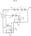
Figure 14 is a circuit diagram of an even further alternativeLED drive circuit 110. - LED drive circuits according to the present invention will be described below with reference to the drawings. It will, however, be noted that the technical scope of the present invention is not limited by any particular embodiment described herein, but extends to the inventions described in the appended claims and their equivalents.
-
Figure 1 is a circuit diagram of anLED drive circuit 10. - As shown in
Figure 1 , theLED drive circuit 10 includes a variable constantcurrent source 15, afirst LED string 11, asecond LED string 12, and a current limitingcircuit 15. - The variable constant
current source 15 is configured to be capable of varying the value of its output current in accordance with an externally supplied control signal (not shown), and outputs the current in the direction shown by an arrow in the figure. - The
first LED string 11 is constructed from a plurality of series-connectedLEDs 11a, and emits a first color of light. Thesecond LED string 12 is constructed from a plurality of series-connectedLEDs 12a, and emits a second color of light. The anodes of theLEDs current source 15 is output. - The current limiting
circuit 14 includes acurrent sensing resistor 14b as a current sensing element, and a depletion-mode FET 14a as a switching element. The drain of theFET 14a is connected to the cathode of thesecond LED string 12, and the source is connected to the right terminal of thecurrent sensing resistor 14b as well as to the cathode of thefirst LED string 11, while the gate is connected to the left terminal of thecurrent sensing resistor 14b which is a terminal to which the output current output from the variable constantcurrent source 15 returns. - The number of series-connected
LEDs 11a contained in thefirst LED string 11 is larger than the number of series-connectedLEDs 12a contained in thesecond LED string 12. That is, the threshold voltage of thefirst LED string 11 is larger than the threshold voltage of thesecond LED string 12. The forward voltage drop of theLED 11a is equal to that of theLED 12a. The threshold voltage is given as the product of the forward voltage drop and the number of series-connected LEDs. The first color of light refers to the color of light whose color temperature is, for example, about 2700 K. TheLED 11a can be produced by coating a blue-emitting LED die with a yellow phosphor. The second color of light refers to the color of light whose color temperature is, for example, about 1600 K. TheLED 12a can be produced by combining a blue-emitting LED die with a phosphor having an emission color between orange and red. - Alternatively, the
second LED string 12 may originally be constructed from LEDs that emit light of low color temperatures such as red or orange. If the forward voltage drop is different between theLED 11a and theLED 12a, the number of series-connected LEDs in thefirst LED string 11 and the number of series-connected LEDs in thesecond LED string 12 are chosen so that the threshold voltage of thesecond LED string 12 given as the product of the forward voltage drop and the number of series-connectedLEDs 12a is smaller than the threshold voltage of thefirst LED string 11. - In the
LED drive circuit 10, the current Io output from the variable constantcurrent source 15 flows into thefirst LED string 11 and thesecond LED string 12. The current I1 passed through thefirst LED string 11 flows into thecurrent sensing resistor 14b, and the current 12 passed through thesecond LED string 12 flows into thecurrent sensing resistor 14b via the drain and source of theFET 14a. -
Figure 2 is a diagram for explaining the operation of theLED drive circuit 10, where the abscissa represents the output current Io of the variable constantcurrent source 15 and the ordinate represents the current I flowing through the various parts. - The operation of the
LED drive circuit 10 will be described below with reference toFigure 2 . The current It flowing through the entireLED drive circuit 10 is the sum of the current I1 flowing through thefirst LED string 11 and the current 12 flowing through thesecond LED string 12. The current It is equal to the output current Io of the variable constantcurrent source 15, and is represented by a straight line having a slope of 45° inFigure 2 . - When the output current Io of the variable constant
current source 15 is small, that is, when the brightness level is decreased, only the current 12 to thesecond LED string 12 flows (It = I2, I1 = 0, the current range indicated by Ia). In this case, the voltage at the current output terminal of the variable constant current source 15 (relative to the voltage at the current return terminal which is assumed to be 0 V; the same applies hereinafter) is larger than the threshold voltage of thesecond LED string 12 but smaller than the threshold voltage of thefirst LED string 11. - The threshold voltage of the LED string here is given as the sum of the forward voltage drops of the series- connected LEDs contained in the LED string. For example, if the LED series circuit contains a total of 10 LEDs each having a forward voltage drop of 3.2 V, the threshold voltage is given as 3.2 (V) × 10 = 32 (V). In the
LED drive circuit 10, if the variation range of the voltage that can stably drive the output terminal of the variable constantcurrent source 15 at a constant current is small, the difference between the number of series-connected LEDs in thefirst LED string 11 and the number of series-connected LEDs in thesecond LED string 12 should be held to about two or three to reduce the difference between their threshold voltages. - The current limiting
circuit 14 sets an upper limit value on the current I2 (as indicated at the right end of the current region Ia). When the current I2 is at its upper limit, if the current I2 is increased, the voltage drop across thecurrent sensing resistor 14b increases, and theFET 14a tries to reduce the current. That is, the current limitingcircuit 14 sets the upper limit value on the current I2 by negative feedback. The upper limit value of the current I2 is determined by the resistance value of thecurrent sensing resistor 14b and the characteristics of theFET 14a. - When the output current Io of the variable constant
current source 15 exceeds the upper limit value of the current limitingcircuit 14, a current equal to the amount by which the current Io exceeds the upper limit value of the current limitingcircuit 14 begins to flow through thefirst LED string 11. Due to this current I1, the voltage drop across thecurrent sensing resistor 14b increases, and the current I2 flowing through theFET 14a decreases. As the current I2 deceases, the current I1 increases correspondingly, but since the rate of decrease of the current I2 is slower than the rate of increase of the current I1, an operating point at which the current I1 and the current I2 flow simultaneously (the voltage at the output terminal of the variable constant current source 15) is determined (It = I1 + I2). - When the output current Io of the variable constant
current source 15 further increases (the current range indicated by Ic), the current flowing through thesecond LED string 12 decreases to 0 (A) (It = I1). - When the output current Io of the variable constant
current source 15 lies within the current range Ia, only thesecond LED string 12 is driven which thus emits light with the second color, and the brightness of the light from thesecond LED string 12 changes as the current Io changes. When the current Io lies within the current range Ib, thefirst LED string 11 and thesecond LED string 12 are simultaneously driven to emit light, and the brightness of the light from each of the first and second LED strings 11 and 12 changes as the current Io changes. Furthermore, since the relative proportions of the brightness of the light of the first color from thefirst LED string 11 and the brightness of the light of the second color from thesecond LED string 12 change as the current Io changes, the color of the light emitted from the LED drive circuit changes. When the output current Io lies within the current range Ic, only thefirst LED string 11 is driven which thus emits light with the first color, and the brightness of the light from thefirst LED string 11 changes as the current Io changes. - Assume that the color temperature of the light (the first color) emitted by the
first LED string 11 is 2700 K and that the color temperature of the light (the second color) emitted by thesecond LED string 12 is 1600 K; then, at low brightness levels (in the current range Ia), theLED drive circuit 10 emits light rich in red. On the other hand, at high brightness levels (in the current range Ic), theLED drive circuit 10 emits white light with reduced redness. At intermediate brightness levels (in the current range Ib), the light emitted from thefirst LED string 11 and the light emitted from thesecond LED string 12 are mixed together, and theLED drive circuit 10 emits light with an intermediate color temperature, with the redness decreasing as the brightness level increases. - While the
first LED string 11 for producing the first emission color has been described as being constructed by combining blue-emitting LED dies with yellow phosphors, the combination for producing the first emission color is not limited to this particular combination. For example, the desired color temperature may be achieved by suitably combining, for example, a red-emitting LED die, a green-emitting LED die, and a blue-emitting LED die. The only requirement is that thefirst LED string 11 be constructed to produce the first emission color as a whole. Similarly, thesecond LED string 12 need only be constructed to produce the second emission color. - While the
LED drive circuit 10 has been described as using thecurrent sensing resistor 14b as the current sensing element, the current sensing element used in theLED drive circuit 10 need not be limited to a resistor. Any element that can control the switching element by detecting the current can be used as the current sensing element; for example, a transistor or a current sensor IC may be used. - It has also been described by way of example that the signal for controlling the variable constant
current source 15 contained in the LED drive circuit is created by processing the output voltage waveform of a dimmer. However, the control signal need not necessarily be limited to the signal created based on the output voltage waveform of the dimmer, but a digital control signal transmitted, for example, from a remote controller or via a power supply line may be used instead. -
Figure 3 is a circuit diagram of an alternativeLED drive circuit 30. - The
LED drive circuit 30 differs from theLED drive circuit 10 only in that thecurrent sensing resistor 14b used in theLED drive circuit 10 is replaced by acurrent sensing resistor 34b (current sensing element) and asource resistor 34c (output resistor) both contained in the current limitingcircuit 34. Here, the cathode of thefirst LED string 11 is connected to the right terminal of thecurrent sensing resistor 34b. -
Figure 4 is a diagram for explaining the operation of theLED drive circuit 30, where the abscissa represents the output current Io of the variable constantcurrent source 15 and the ordinate represents the current I flowing through the various parts. - The operation of the
LED drive circuit 30 will be described below with reference toFigure 4 . The current It flowing through the entireLED drive circuit 30 is the sum of the current I1 flowing through thefirst LED string 11 and the current I2 flowing through thesecond LED string 12. The current It is equal to the output current Io of the variable constantcurrent source 15, and is represented by a straight line having a slope of 45° inFigure 4 . - The difference between
Figure 4 andFigure 2 is that the intermediate current region Ib2 shown inFigure 4 is wider than the current region Ib shown inFigure 2 . As a result, in the current region Ib2, the current I2 flowing through thesecond LED string 12 decreases more gradually than inFigure 2 , and similarly, the current I1 flowing through thefirst LED string 11 increases more gradually. This is because, when the voltage drop across a composite resistor formed by combining thesource resistor 34c with thecurrent sensing resistor 34b is fed back to theFET 14a, the proportion of the current I1 flowing through thefirst LED string 11 that can contribute to the feedback is reduced compared with the case ofFigure 2 . Thecurrent sensing resistor 34b constitutes a part of the composite resistor, and the value of thecurrent sensing resistor 34b is chosen to be smaller than the value of thecurrent sensing resistor 14b. For example, the values may be chosen so that the relation R14b = R34b + R34c holds. R14b is the resistance value of thecurrent sensing resistor 14b, R34b is the resistance value of thecurrent sensing resistor 34b, and R34c is the resistance value of thesource resistor 34c. - As a result, the intermediate current range Ib2 in the
LED drive circuit 30 becomes wider than the corresponding current range in theLED drive circuit 10, and the change from the first color to the second color in the color of emission becomes smoother. Further, the position and width of the intermediate current region can be changed by adjusting the resistance values R14b, R34b, and R34c. -
Figure 5 is a circuit diagram of another alternativeLED drive circuit 50. - The
LED drive circuit 50 differs from theLED drive circuit 10 only in that thefirst LED string 11 in theLED drive circuit 10 is divided into afirst LED string 51 and athird LED string 53, and the anode of thefirst LED string 51 and the anode of thesecond LED string 12 are connected to the cathode of thethird LED string 53. - The number of series-connected
LED 51a contained in the first LED string 51 (the threshold voltage of the first LED string 51) is chosen to be larger than the number of series-connectedLED 12a contained in the second LED string 12 (the threshold voltage of the second LED string 12). In the current limitingcircuit 54, thecurrent sensing resistor 54b as the current sensing element is often adjusted to a value different from that of thecurrent sensing resistor 14b shown inFigure 1 . - The
LED drive circuit 50 is designed so that when the variable constantcurrent source 15 is supplying a large current Io, thesecond LED string 12 is turned off and thefirst LED string 51 and thethird LED string 53 are both driven to emit light. That is, when the variable constantcurrent source 15 is supplying a large current Io, theLED drive circuit 50 operates in the same manner as theLED drive circuit 10 ofFigure 1 operating in the current region Ic (seeFigure 2 ). At this time (when the dimmer is set to a high brightness level), the color of the light emitted from theLED drive circuit 50 is the same as that of theLED drive circuit 10. - On the other hand, when the variable constant
current source 15 is supplying an intermediate current Io (which corresponds to the current region Ib shown inFigure 2 ), or when the variable constantcurrent source 15 is supplying a small current Io (which corresponds to the current region Ia shown inFigure 2 ), since thethird LED string 53 is driven to emit light, the color of the light emitted from theLED drive circuit 50 is different from that of theLED drive circuit 10. -
Figure 6 is a circuit diagram of still another alternativeLED drive circuit 60. - The
LED drive circuit 60 differs from theLED drive circuit 10 in that theLED drive circuit 60 further includes afourth LED string 63, which is connected in parallel with thefirst LED string 11 and thesecond LED string 12, and an additional current limitingcircuit 65. In theLED drive circuit 60, the number of parallel-connected LED strings is increased by adding thefourth LED string 63 and the current limitingcircuit 65. - In the
LED drive circuit 60, the number of series-connectedLEDs 11a contained in the first LED string 11 (the threshold voltage of the first LED string 11), the number of series-connectedLEDs 12a contained in the second LED string 12 (the threshold voltage of the second LED string 12), and the number of series-connectedLEDs 63a contained in the fourth LED string 63 (the threshold voltage of the fourth LED string 63) are respectively chosen so that the number of series-connected LEDs (the threshold voltage) decreases in the order named. The value of thecurrent sensing resistor 64b (current sensing element) contained in the current limitingcircuit 64 is chosen to be smaller than the value of thecurrent sensing resistor 65b (second current sensing element) contained in the current limitingcircuit 65, and the left terminal of thecurrent sensing resistor 64b is connected to the right terminal of thecurrent sensing resistor 65b. - In the
LED drive circuit 60, when the variable constantcurrent source 15 is supplying a small current Io, only thefourth LED string 63 is driven to emit light. When the variable constantcurrent source 15 increases the current Io, thefourth LED string 63 turns off, and only thesecond LED string 12 is driven to emit light. When the variable constantcurrent source 15 further increases the current Io, thesecond LED string 12 turns off, and only thefirst LED string 11 is driven to emit light. - As described above, in the
LED drive circuit 60, the number of parallel-connected LED strings, two in theLED drive circuit 10, is increased to three by adding thefourth LED string 63 and the current limitingcircuit 65. By thus increasing the number of parallel-connected LED strings, theLED drive circuit 60 can increase the degree of freedom with which the color of the emitted light can be changed as the light output is controlled. -
Figure 7 is a circuit diagram of yet another alternativeLED drive circuit 70. - The
LED drive circuit 70 differs from theLED drive circuit 10 only in that the current limitingcircuit 14 contained in theLED drive circuit 10 is replaced by a current limitingcircuit 70x as shown inFigure 7 . - The current limiting
circuit 70x includes an enhancement-mode FET 71 as a switching element, acurrent sensing resistor 73 as a current sensing element, a pull-upresistor 74, and abipolar transistor 72. The drain of theFET 71 is connected to the top terminal of the pull-upresistor 74 and the cathode of thesecond LED string 12. The gate of theFET 71 is connected to the bottom terminal of the pull-upresistor 74 and the collector of thetransistor 72. The source of theFET 71 is connected to the top terminal of thecurrent sensing resistor 73, the base of thetransistor 72, and the cathode of thefirst LED string 11. The bottom terminal of thecurrent sensing resistor 73 is connected to the emitter of thetransistor 72 and the current return terminal of the variable constantcurrent source 15. - The current limiting
circuit 70x is a well known circuit as a current limiting circuit or a constant current circuit. When negative feedback is applied to maintain the base-emitter voltage at 0.6 V, the current limitingcircuit 70x acts to limit the current 12 flowing through thesecond LED string 12. Further, when the current I1 flowing through thefirst LED string 11 increases, and thetransistor 72 saturates, theFET 71 cuts off. That is, this circuit operates in a manner similar to the current limitingcircuit 14, etc., contained in theLED drive circuit 10, etc. - In each of the
LED drive circuits Figures 1 ,3 ,5 , and6 , use has been made of the depletion-mode FET 14a as the switching element in the current limitingcircuit Figure 7 . -
Figure 8 is a circuit diagram of a further alternativeLED drive circuit 80. - The
LED drive circuit 80 differs from theLED drive circuit 10 only by the inclusion of afifth LED string 85. Thefifth LED string 85 is constructed from a plurality of series-connectedLEDs 85a, and its anode is connected to the current output terminal of the variable constantcurrent source 15, while its cathode is connected to the current return terminal of the variable constantcurrent source 15. Thefifth LED string 85 emits light with the first color, as in the case of thefirst LED string 11. The number of series-connectedLEDs 85a contained in thefifth LED string 85 is larger only by one than the number of series-connectedLEDs 11a contained in thefirst LED string 11. TheLEDs 11a and theLEDs 85a are the same LEDs. - When the
FET 14a cuts off, the voltage drop that develops across thecurrent sensing resistor 14b is 3 V, and the forward voltage drop of eachLED 85a is chosen to be slightly larger than 3 V. In the current regions Ia and Ib shown inFigure 2 , theLED drive circuit 80 operates in the same manner as theLED drive circuit 10 shown inFigure 1 . That is, in the current region Ia, only thesecond LED string 12 is driven to emit light, while in the current region Ib, thefirst LED string 11 and thesecond LED string 12 are both driven to emit light. In the current regions Ia and Ib, the current flowing through thefifth LED string 85 is 0 (A). - When the output current Io of the variable constant
current source 15 is equal to the current that causes theFET 14a to cut off (inFigure 2 , the left end of the current region Ic), the voltage drop that develops across thecurrent sensing resistor 14b is 3 V. Since the threshold voltage of thefifth LED string 85 is a little more than 3 V higher than the threshold voltage of thefirst LED string 11, the current I1 flows through the first LED string 11 (I1 = Io), and no current flows through the fifth LED string 85 (15 = 0). When the current Io is increased, and the voltage drop across thecurrent sensing resistor 14b becomes larger than the forward voltage drop of eachLED 85a, the current I5 begins to flow through thefifth LED string 85. - In the
LED drive circuit 80, power loss is reduced because the current I5 flowing through thefifth LED string 85 does not pass through thecurrent sensing resistor 14b. That is, according to theLED drive circuit 80, lighting equipment can be provided that not only can vary the color of the emitted light when controlling the light output by adjusting the current Io, but can also achieve high brightness and high power utilization when the variable constantcurrent source 15 is supplying a large current Io. -
Figure 9 is a circuit diagram of a still further alternativeLED drive circuit 90. - The
LED drive circuit 90 is constructed by combining theLED drive circuit 30 shown inFigure 3 and theLED drive circuit 60 shown inFigure 6 . In theLED drive circuit 90, thefirst LED string 91, thesecond LED string 92, thefourth LED string 93, and the current limitingcircuits first LED string 11, thesecond LED string 12, thefourth LED string 63, and the current limitingcircuits LED drive circuit 60. In theLED drive circuit 90, as in theLED drive circuit 30, the current limitingcircuits FET source resistor current sensing resistor - The
first LED string 91 is constructed from five parallel-connected LED strings 911, 912, 913, 914, and 915, each constructed by connecting 12LEDs 91a in series. TheLED string 91 is equivalent to an LED string constructed from 12 series-connected LED arrays each comprising five parallel-connected LEDs 91a. The reason that thefirst LED string 91 is constructed in the form of a series-parallel circuit is to prevent the current from concentrating on anyparticular LEDs 91a and thereby prevent heat dissipation efficiency and light emission efficiency from dropping when causing theLED drive circuit 90 to emit light with high brightness. Thesecond LED string 92 is constructed by connecting nineLEDs 92a in series, and thefourth LED string 93 is constructed by connecting sevenLEDs 93a in series. For example, thecurrent sensing resistors source resistors LED drive circuit 90 is essentially the same as the method of interconnecting the various elements in the respectiveLED drive circuits -
Figure 10 is a graph for explaining the operation of theLED drive circuit 90, where the abscissa represents the output current Io of the variable constantcurrent source 15 and the ordinate represents the current I flowing through the various parts. - The operation of the
LED drive circuit 90 will be described below with reference toFigure 10 . The current It flowing through the entireLED drive circuit 90 is the sum of the current I1 flowing through thefirst LED string 91, the current 12 flowing through thesecond LED string 92, and the current 14 flowing through thefourth LED string 93. The current It is equal to the output current Io of the variable constantcurrent source 15, and is represented by a straight line having a slope of 45° inFigure 10 . - In the
LED drive circuit 90, when the output current Io of the variable constantcurrent source 15 is small, that is, when the brightness level is decreased, only the current I4 to thefourth LED string 93 flows (It = I4, I1 = I2 = 0, the current range indicated by Ia3). When the current Io increases and exceeds the maximum current of the current limitingcircuit 94, the current 12 begins to flow through the second LED string 92 (It = I2 + I4, I1 = 0, the current range indicated by Ib3). When the current Io further increases, theFET 94a in the current limitingcircuit 94 cuts off (It = I2, I1 = I4 = 0, the current range indicated by Ic3). When the current Io further increases and exceeds the maximum current of the current limitingcircuit 95, the current I1 begins to flow through the first LED string 91 (It = I1 + I2, I4 = 0, the current range indicated by Id3). When the current Io further increases, and theFET 95a in the current limitingcircuit 95 cuts off, the current flowing as the current It is only the current I1 (It = I1, I2 = I4 = 0, the current range indicated by Ie3). - The operation of the
LED drive circuit 90 is basically the same as that of theLED drive circuit 60, but differs in that the period (current range Ib3) during which thesecond LED string 92 and thefourth LED string 93 are simultaneously driven to emit light and the period (current range Id3) during which thefirst LED string 91 and thesecond LED string 92 are simultaneously driven to emit light are longer, as in theLED drive circuit 30. -
Figure 11 is a diagram for explaining how the color of light emitted from theLED drive circuit 90 changes, where the abscissa and the ordinate respectively represent the chromaticity coordinates x and y of a CIE color system. - Referring to
Figure 11 , a description will be given below of how the color of the light emitted from theLED drive circuit 90 changes. InFigure 11 , apoint 111 indicates the chromaticity coordinates for 2700 K representing the emission color of thefirst LED string 91, apoint 112 indicates the chromaticity coordinates of the emission color of thesecond LED string 92, and apoint 113 indicates the chromaticity coordinates for 1600 K representing the emission color of thefourth LED string 93. Acurve 115 shown as a dotted line represents the black body locus. - The color of the light emitted from the
LED drive circuit 90 changes along abroken line 114 shown as a solid line. When the output current Io (seeFigure 10 ) of the variable constant current source 15 (seeFigure 9 ) is increased (the light output is increased from low to high), the color of the light emitted from theLED drive circuit 90 changes from thepoint 113 toward the point 112 (from the current range Ia3 to the current range Ic3 through the current range Ib3 inFigure 10 ). When the output current Io of the variable constant current source 15 (seeFigure 9 ) is further increased, the color of the emitted light changes from thepoint 112 toward the point 111 (from the current range Ic3 to the current range Ie3 through the current range Id3 inFigure 10 ). - In
Figure 11 , the dashedline 116 indicates the change of the color of the light emitted from the LED drive circuit 10 (seeFigure 1 ). In the two-colorLED drive circuit 10 having only the first and second LED strings 11 and 12, when thefirst LED string 11 emits light at 2700 K, and thesecond LED string 12 emits light at 1600 K, the color of the emitted light changes as indicated by the dashedline 116. As a result, when an object is illuminated with light whose color is deviated from the black body locus, theLED drive circuit 10 is unable to render the color of the object (object color) faithfully. - By contrast, the
LED drive circuit 60 can continue to maintain the color of the emitted light close to the back body locus, which is not possible with theLED drive circuit 10. TheLED drive circuit 60, unlike the two-color drive circuit, can render the object color so that it will appear natural. InFigure 11 , thepoint 112 is located at a position higher than theblack body curve 115. Thepoint 112 need only be located at a position near the region (the x value is approximately 0.48 to 0.54) where theblack body curve 115 is substantially flat, and preferably, it is positioned near the peak (the x value is approximately 0.51) of thecurve 115. - In the
LED drive circuit 90, the period Ib3 (seeFigure 10 ) during which thesecond LED string 92 and thefourth LED string 93 are simultaneously driven to emit light and the period Id3 (seeFigure 10 ) during which thefirst LED string 91 and thesecond LED string 92 are simultaneously driven to emit light are set longer than the corresponding periods of theLED drive circuit 60. Accordingly, with theLED drive circuit 90, the color of the emitted light can be changed in much the same way as controlling the light output of an incandescent lamp with a dimmer. - While the
LED drive circuit 90 has been described by assuming that thefirst LED string 91 emits light at 2700 K and thefourth LED string 93 emits light at 1600 K, the combination of the emission colors is not limited to this particular combination. For example, since colors of high color temperatures are preferred in Japan, thefirst LED string 91 may be configured to emit light at about 6500 K. Even when the emission color of thefirst LED string 91 is set to about 6500 K, it is preferable that the color of the emitted light as a whole is made to change so as to substantially follow the black body locus as the light output is changed. For example, in the CIE color system, the x component of the chromaticity coordinates describing the emission color of thesecond LED string 92 is set at a point intermediate between the chromaticity coordinates describing the emission color of thefirst LED string 91 and the chromaticity coordinates describing the emission color of thefourth LED string 93. Then, the y component of the chromaticity coordinates describing the emission color of thesecond LED string 92 is set so that the broken line connecting the chromaticity coordinates of the emission color of thefirst LED string 91, the chromaticity coordinates of the emission color of thesecond LED string 92, and the chromaticity coordinates describing the emission color of thefourth LED string 93 substantially follows the black body locus. When the x and y components of the chromaticity coordinates describing the emission color of thesecond LED string 92 are set as described above, theLED drive circuit 90 can be configured to produce light whose color changes so as to substantially follow the black body locus as the light output is changed, even when the emission color of thefirst LED string 91 is set to about 6500 K. - In the
LED drive circuit 90, the emission color of thefourth LED string 93 has been set to 1600 K, and the color of the emitted light as a whole has been made to change in such a manner as to resemble the black body locus. However, if thefourth LED string 93 is configured to emit light of a color (for example, blue) noticeable in darkness while maintaining the circuit configuration of theLED drive circuit 90 unchanged, the light produced by driving only thefourth LED string 93 can be used as a night-light. In this case, the number of series-connected LEDs in thefourth LED string 93 must be reduced, and the emission color of thesecond LED string 92 must be set to about 1600 K. -
Figure 12 is a circuit diagram of a yet further alternativeLED drive circuit 100. - As shown in
Figure 12 , theLED drive circuit 100 includes a variable constantcurrent source 15, afirst LED string 11, asecond LED string 12, and a current limitingcircuit 114. Thefirst LED string 11, thesecond LED string 12, and the variable constantcurrent source 15 are the same as thefirst LED string 11, thesecond LED string 12, and the variable constantcurrent source 15 contained in theLED drive circuit 10 shown inFigure 1 . - The anode of the
first LED string 11 is connected to the current output terminal of the variable constantcurrent source 15, and the cathode is connected to the right terminal of acurrent sensing resistor 114b which is a current sensing element contained in the current limitingcircuit 114. The anode of thesecond LED string 12 is connected to the source of anFET 114a contained in the current limitingcircuit 114, and the cathode is connected to the right terminal of thecurrent sensing resistor 114b. - The current limiting
circuit 114 includes, in addition to the depletion-mode FET 114a as a switching element and thecurrent sensing resistor 114b, a pull-upresistor 114c and abipolar transistor 114d. The drain of theFET 114a and the upper terminal of the pull-upresistor 114c are connected to the anode of thefirst LED string 11. The gate of theFET 114a and the lower terminal of the pull-upresistor 114c are connected to the collector of thetransistor 114d. The base of thetransistor 114d is connected to the right terminal of thecurrent sensing resistor 114b. The emitter of thetransistor 114d and the left terminal of thecurrent sensing resistor 114b are connected to the current return terminal of the variable constantcurrent source 15. - The major differences between the
LED drive circuit 100 and theLED drive circuit 10 are that, in theLED drive circuit 100, theFET 114a used as the switching element is disposed on the anode side of thesecond LED string 12 and that an amplifying circuit constructed from a combination of the pull-upresistor 114c and thetransistor 114d is inserted. With the provision of the amplifying circuit, if the voltage across thecurrent sensing resistor 114b only slightly exceeds 0.6 V (the base-emitter forward voltage drop of the silicon transistor), the gate voltage of theFET 114a drops, and theFET 114a cuts off. Accordingly, theLED drive circuit 100 exhibits behavior such that when the output current Io of the variable constantcurrent source 15 is increased gradually, and the current Io reaches a specific value, the second LED string turns off and the first LED string turns on. - The
LED drive circuit 100 can be regarded as a modification of theLED drive circuit 70 shown inFigure 7 . For example, if, in theLED drive circuit 70, thesecond LED string 12 is disposed between theFET 71 and thecurrent sensing resistor 73, theLED drive circuit 70 becomes identical in configuration to theLED drive circuit 100. More specifically, in theLED drive circuit 70, the anode of thesecond LED string 12 is connected to the source of theFET 71, the cathode of thesecond LED string 12 is connected to the upper terminal of thecurrent sensing resistor 73, and the drain of theFET 71 and the upper terminal of theresistor 74 are connected to thefirst LED string 11; then, the configuration is the same as that of theLED drive circuit 100. -
Figure 13 is a diagram for explaining the operation of theLED drive circuit 100, where the abscissa represents the output current Io of the variable constantcurrent source 15 and the ordinate represents the current I flowing through the various parts. - The operation of the
LED drive circuit 100 will be described below with reference toFigure 13 . The current It flowing through the entireLED drive circuit 100 is the sum of the current I1 flowing through thefirst LED string 11 and the current I2 flowing through thesecond LED string 12. The current It is equal to the output current Io of the variable constantcurrent source 15, and is represented by a straight line having a slope of 45° inFigure 13 . - In
Figure 13 , when the output current Io of the variable constantcurrent source 15 is small, that is, when the brightness level is decreased, only the current 12 to thesecond LED string 12 flows (It = 12, I1 = 0, the current range indicated by Ia). In this case, the voltage at the current output terminal of the variable constant current source 15 (relative to the voltage at the current return terminal which is assumed to be 0 V; the same applies hereinafter) is larger than the threshold voltage of thesecond LED string 12 but smaller than the threshold voltage of thefirst LED string 11. - The threshold voltage of the LED string here is given as the sum of the forward voltage drops of the series- connected LEDs contained in the LED string; for example, if the LED series circuit is constructed from a total of 10 LEDs each having a forward voltage drop of 3.2 V, the threshold voltage is given as 3.2 (V) × 10 = 32 (V). In the
LED drive circuit 100, if the variation range of the voltage that can stably drive the output terminal of the variable constantcurrent source 15 at a constant current is small, the difference between the number of series-connected LEDs in thefirst LED string 11 and the number of series-connected LEDs in thesecond LED string 12 should be held to about two or three to reduce the difference between their threshold voltages. - The current limiting
circuit 114 sets an upper limit value on the current I2 (as indicated at the right end of the current region Ia). When the current I2 is at its upper limit, the voltage developed across thecurrent sensing resistor 114b is 0.6 V. When the current 12 is further increased from this condition, the collector-emitter part of thetransistor 114d turns on. As a result, theFET 114a cuts off, the current I2 is reduced to 0 (A), and the current I1 flows through thefirst LED string 11. Since this change occurs abruptly, the rate of change of each of the currents I1 and I2 in the current range Ib inFigure 13 is larger (steeper) than the rate of change of each of the currents I1 and I2 in the current range Ib inFigure 2 . - When the output current Io of the variable constant
current source 15 further increases beyond the upper limit value (into the current range Ic), the current flowing as the current It is only the current I1 flowing through the first LED string 11 (It = I1). - In the
LED drive circuit 100, the color temperature of the emission color (the first color) of thefirst LED string 11 and the color temperature of the emission color (the second color) of thesecond LED string 12 can be set, for example, to 2700 K and 1600 K, respectively. In this case, when set in the high brightness range (the current range Ic), theLED drive circuit 100 operates to produce light with high color temperatures, and when set in the low brightness range (the current range Ia), theLED drive circuit 100 operates to produce light with color temperatures with increased redness, and the intermediate brightness range (the current range Ib) can be virtually eliminated. - The
LED drive circuit 100 has been described as using the depletion-mode FET 114a as the switching element. However, in the case of theFET 114a used in theLED drive circuit 100, unlike theFET 14a in theLED drive circuit 10, the threshold characteristics unique to the depletion-mode FET are not used to set the upper limit value of the current. In theLED drive circuit 100, the upper limit value of the current is determined by the current limitingresistor 114b and the base-emitter forward voltage drop of thetransistor 114d. Therefore, theFET 114a in theLED drive circuit 100 may be replaced by an enhancement-mode FET or a bipolar transistor. Further, thetransistor 114d in theLED drive circuit 100 may be replaced by a combination of a reference voltage source and a comparator. -
Figure 14 is a circuit diagram of an even further alternativeLED drive circuit 110. - The
LED drive circuit 110 shown inFigure 14 differs from theLED drive circuit 100 shown inFigure 12 only in that the current limitingcircuit 114 in theLED drive circuit 100 is replaced by a current limiting circuit 114' in theLED drive circuit 110. In the current limiting circuit 114', thecurrent sensing resistor 114b in the current limitingcircuit 114 shown inFigure 12 is replaced by aresistor 114e, athermistor 114f, and aresistor 114g. - In the
LED drive circuit 100 shown inFigure 12 , the forward voltage drops of theLEDs transistor 114d change with temperature. Accordingly, in theLED drive circuit 100, since the current range Ib is narrow (seeFigure 13 ), there is the possibility that the LED string emitting light with high color temperatures (like the first LED string) may come to emit light with low color temperatures (like the second LED string) when the temperature changes. - To address this, in the
LED drive circuit 110 shown inFigure 14 , a temperature compensating function is incorporated in the current sensing resistor by using theresistor 114e,thermistor 114f, andresistor 114g. Instead of incorporating the temperature compensating function in the current sensing resistor, the temperature compensating function may be incorporated in the variable constantcurrent source 15. However, in theLED drive circuit 100 shown inFigure 12 , since the variable constantcurrent source 15 is an independent circuit block separately provided from the other parts, it is easier to handle the circuit if the temperature compensating function is incorporated in the current sensing resistor, as in theLED drive circuit 110 shown inFigure 14 . -
- 10, 30, 50, 60, 70, 80, 90, 100, 110 ... LED DRIVE CIRCUIT
- 11, 51, 91 ... FIRST LED STRING
- 11a, 12a, 51a, 53a, 63a, 85a, 91a, 92a, 93a ... LED
- 12, 92 ... SECOND LED STRING
- 14, 34, 54, 64, 65, 70x, 94, 95, 114, 114' ... CURRENT LIMITING CIRCUIT
- 14a, 94a, 95a ... DEPLETION-MODE FET
- 14b, 34b, 54b, 64b, 65b, 73, 94b, 95b ... CURRENT SENSING RESISTOR
- 34c, 94c, 95c ... SOURCE RESISTOR
- 53 ... THIRD LED STRING
- 63, 93 ... FOURTH LED STRING
- 71 ... ENHANCEMENT-MODE FET
- 72 ... BIPOLAR TRANSISTOR
- 74 ... PULL-UP RESISTOR
- 85 ... FIFTH LED STRING
- 111, 112, 113 ... CHROMATICITY COORDINATES
- 114f ... THERMISTOR
Claims (10)
- An LED drive circuit comprising:a variable constant current source;a first LED string having a plurality of series-connected LEDs and configured to emit a first color of light;a second LED string having a plurality of series-connected LEDs and configured to emit a second color of light; anda current limiting circuit containing a current sensing element and a switching element, whereinthe first LED string has a larger threshold voltage than the second LED string,the first LED string and the second LED string are connected in parallel with each other to the variable constant current source, andthe current limiting circuit limits a current flowing through the second LED string, based on a current flowing into the current sensing element via the first LED string.
- The LED drive circuit according to claim 1, further comprising a third LED string disposed between the variable constant current source and the first and second LED strings.
- The LED drive circuit according to claim 1, further comprising:a third LED string which is connected in parallel with the first and second LED strings to the variable constant current source; andan additional current limiting circuit containing a second current sensing element and a second switching element, and whereinthe additional current limiting circuit limits a current flowing through the third LED string, based on a current flowing into the second current sensing element.
- The LED drive circuit according to claim 1, further comprising a third LED string, and whereinan anode of the third LED string is connected to a terminal at which a current from the variable constant current source 15 is output, and a cathode of the third LED string is connected to a terminal through which the current output from the variable constant current source 15 is fed back.
- The LED drive circuit according to any one of claims 1 to 4, further comprising an output resistor which is connected between the current sensing element and a current output terminal of the switching element.
- The LED drive circuit according to any one of claims 1 to 5, wherein the switching element is a depletion-mode FET.
- The LED drive circuit according to any one of claims 1 to 5, wherein the current limiting circuit contains a bipolar transistor, the current sensing element is connected between a base and emitter of the bipolar transistor, and the switching element is controlled by a voltage output from a collector of the bipolar transistor.
- The LED drive circuit according to claim 7, wherein the switching element is an enhancement-mode FET.
- The LED drive circuit according to claim 7 or 8, wherein the current sensing element includes a thermistor.
- The LED drive circuit according to claim 3, wherein the emission color of the second LED string, plotted as chromaticity coordinates in a CIE color system, is located between the emission color of the first LED string plotted as chromaticity coordinates and the emission color of the third LED string plotted as chromaticity coordinates, and a broken line connecting the chromaticity coordinates of the respective emission colors substantially follows a black body locus.
Applications Claiming Priority (3)
| Application Number | Priority Date | Filing Date | Title |
|---|---|---|---|
| JP2014182212 | 2014-09-08 | ||
| JP2015018234 | 2015-02-02 | ||
| PCT/JP2015/075486 WO2016039344A1 (en) | 2014-09-08 | 2015-09-08 | Led drive circuit |
Publications (3)
| Publication Number | Publication Date |
|---|---|
| EP3193564A1 true EP3193564A1 (en) | 2017-07-19 |
| EP3193564A4 EP3193564A4 (en) | 2018-04-11 |
| EP3193564B1 EP3193564B1 (en) | 2021-04-07 |
Family
ID=55459088
Family Applications (1)
| Application Number | Title | Priority Date | Filing Date |
|---|---|---|---|
| EP15839840.4A Active EP3193564B1 (en) | 2014-09-08 | 2015-09-08 | Led drive circuit |
Country Status (5)
| Country | Link |
|---|---|
| US (1) | US10182486B2 (en) |
| EP (1) | EP3193564B1 (en) |
| JP (1) | JP6482563B2 (en) |
| CN (1) | CN106605449B (en) |
| WO (1) | WO2016039344A1 (en) |
Cited By (1)
| Publication number | Priority date | Publication date | Assignee | Title |
|---|---|---|---|---|
| EP3525552A1 (en) * | 2018-02-09 | 2019-08-14 | ZKW Group GmbH | Circuit arrangement for switching on and off at least two light strands for a vehicle headlight electrically connected in parallel |
Families Citing this family (18)
| Publication number | Priority date | Publication date | Assignee | Title |
|---|---|---|---|---|
| US11266014B2 (en) | 2008-02-14 | 2022-03-01 | Metrospec Technology, L.L.C. | LED lighting systems and method |
| US8007286B1 (en) | 2008-03-18 | 2011-08-30 | Metrospec Technology, Llc | Circuit boards interconnected by overlapping plated through holes portions |
| EP3282491B1 (en) * | 2015-04-08 | 2019-10-09 | Citizen Watch Co., Ltd. | Led drive circuit |
| KR102121545B1 (en) | 2016-05-27 | 2020-06-11 | 광동 오포 모바일 텔레커뮤니케이션즈 코포레이션 리미티드 | Battery protection board, battery and mobile terminal |
| JP6872732B2 (en) * | 2017-04-18 | 2021-05-19 | パナソニックIpマネジメント株式会社 | lighting equipment |
| CN107027225B (en) * | 2017-06-15 | 2019-01-29 | 乐健科技(珠海)有限公司 | The light-dimming method of LED light adjusting circuit and LED module, LED module |
| JP6535840B2 (en) * | 2017-11-13 | 2019-07-03 | Zigenライティングソリューション株式会社 | Light emitting device |
| WO2019092899A1 (en) * | 2017-11-13 | 2019-05-16 | Zigenライティングソリューション株式会社 | Light-emitting device |
| US10874001B2 (en) * | 2018-01-26 | 2020-12-22 | Lumens Co., Ltd. | Color temperature variable light emitting diode module, lighting device using the light emitting diode module and method for fabricating the light emitting diode module |
| JP6527982B1 (en) * | 2018-03-28 | 2019-06-12 | 洋一 尾▲崎▼ | LED lighting device |
| JP2020030905A (en) * | 2018-08-21 | 2020-02-27 | シチズン時計株式会社 | Led light-emitting device |
| US10849200B2 (en) * | 2018-09-28 | 2020-11-24 | Metrospec Technology, L.L.C. | Solid state lighting circuit with current bias and method of controlling thereof |
| CN109640459B (en) * | 2019-01-29 | 2021-01-19 | 无锡奥利杰科技有限公司 | Switch color temperature adjusting control circuit based on LED illumination linear driving condition |
| EP3790362B1 (en) * | 2019-09-03 | 2022-03-02 | ROBE lighting s.r.o. | System and method for matching light output from led luminaires |
| CN113966031B (en) * | 2020-07-01 | 2024-11-12 | 赛万特科技有限责任公司 | Cabinet light interface device and lighting device interface device |
| CN113225868A (en) * | 2021-04-19 | 2021-08-06 | 科特亚照明(上海)有限公司 | Color temperature switching circuit controlled by single switching tube |
| US11622431B2 (en) * | 2021-06-30 | 2023-04-04 | Western Digital Technologies, Inc. | Method and apparatus to control bi-color LEDs on enterprise and datacenter solid state drive (E3) form factor |
| US12538406B2 (en) | 2022-12-20 | 2026-01-27 | Electronic Theatre Controls, Inc. | Independent lighting control |
Family Cites Families (17)
| Publication number | Priority date | Publication date | Assignee | Title |
|---|---|---|---|---|
| WO2006019897A2 (en) * | 2004-08-04 | 2006-02-23 | Ng James K | Led lighting system |
| KR101345354B1 (en) | 2006-10-06 | 2013-12-30 | 코닌클리케 필립스 엔.브이. | Light element array with controllable current sources and method of operation |
| EP2302706A4 (en) * | 2008-07-15 | 2012-02-15 | Sharp Kk | Light emitting element driving circuit |
| US7936132B2 (en) | 2008-07-16 | 2011-05-03 | Iwatt Inc. | LED lamp |
| US9433046B2 (en) | 2011-01-21 | 2016-08-30 | Once Innovations, Inc. | Driving circuitry for LED lighting with reduced total harmonic distortion |
| RU2012109542A (en) * | 2009-08-14 | 2013-09-20 | Уанс Инновейшнз, Инк. | HARMONIC DISTORTION REDUCTION FOR LED LOADS |
| WO2011053708A1 (en) | 2009-10-28 | 2011-05-05 | Once Innovations, Inc. | Architecture for high power factor and low harmonic distortion led lighting |
| EP2644006B1 (en) | 2010-11-25 | 2018-03-28 | Philips Lighting Holding B.V. | Illumination system comprising a plurality of leds |
| US8779675B2 (en) * | 2010-12-16 | 2014-07-15 | Cooper Technologies Company | Controlling current flowing through LEDs in a LED lighting fixture |
| US8710754B2 (en) * | 2011-09-12 | 2014-04-29 | Juno Manufacturing Llc | Dimmable LED light fixture having adjustable color temperature |
| WO2013051658A1 (en) * | 2011-10-04 | 2013-04-11 | シチズンホールディングス株式会社 | Led illumination device |
| US9408278B2 (en) | 2012-02-07 | 2016-08-02 | Panasonic Intellectual Property Management Co., Ltd. | Light-emitting circuit with variable resistor element, and light-emitting module and illumination device including the same |
| WO2013158921A1 (en) | 2012-04-18 | 2013-10-24 | Axlen, Inc. | Solid-state light source |
| TWI457048B (en) * | 2012-06-07 | 2014-10-11 | Polytronics Technology Corp | Illumination apparatus and power supply voltage management method thereof |
| JP5185468B1 (en) * | 2012-12-07 | 2013-04-17 | トキコーポレーション株式会社 | Lighting device and control circuit |
| JP2014157744A (en) | 2013-02-15 | 2014-08-28 | Panasonic Corp | Light emitting circuit, light emitting module and lighting apparatus |
| US9277615B2 (en) * | 2013-02-18 | 2016-03-01 | Citizen Holdings Co., Ltd. | LED drive circuit |
-
2015
- 2015-09-08 WO PCT/JP2015/075486 patent/WO2016039344A1/en not_active Ceased
- 2015-09-08 EP EP15839840.4A patent/EP3193564B1/en active Active
- 2015-09-08 CN CN201580048063.7A patent/CN106605449B/en active Active
- 2015-09-08 US US15/509,278 patent/US10182486B2/en active Active
- 2015-09-08 JP JP2016547455A patent/JP6482563B2/en active Active
Cited By (2)
| Publication number | Priority date | Publication date | Assignee | Title |
|---|---|---|---|---|
| EP3525552A1 (en) * | 2018-02-09 | 2019-08-14 | ZKW Group GmbH | Circuit arrangement for switching on and off at least two light strands for a vehicle headlight electrically connected in parallel |
| CN110139421A (en) * | 2018-02-09 | 2019-08-16 | Zkw集团有限责任公司 | Circuit arrangement for alternately switching on and off at least two electrically parallel lamp branches of a headlight |
Also Published As
| Publication number | Publication date |
|---|---|
| CN106605449A (en) | 2017-04-26 |
| EP3193564A4 (en) | 2018-04-11 |
| US10182486B2 (en) | 2019-01-15 |
| WO2016039344A1 (en) | 2016-03-17 |
| US20170280532A1 (en) | 2017-09-28 |
| EP3193564B1 (en) | 2021-04-07 |
| JPWO2016039344A1 (en) | 2017-06-15 |
| CN106605449B (en) | 2019-06-04 |
| JP6482563B2 (en) | 2019-03-13 |
Similar Documents
| Publication | Publication Date | Title |
|---|---|---|
| EP3193564B1 (en) | Led drive circuit | |
| EP3446546B1 (en) | A method of controlling a lighting arrangement and a lighting control circuit | |
| US9730291B1 (en) | Color temperature adjustment based on dim level | |
| TWI613930B (en) | Multi-string dimmable led driver | |
| US8917026B2 (en) | Linear bypass electrical circuit for driving LED strings | |
| CN102318440B (en) | Many LED control | |
| US11812525B2 (en) | Methods and apparatus for controlling the current supplied to light emitting diodes | |
| US9860944B2 (en) | LED driver circuit | |
| JP6087828B2 (en) | LED string driving method and driving device | |
| EP2797386B1 (en) | A dimmable LED lighting circuit, a controller therefor and method of controlling a dimmable LED lighting circuit | |
| JP2013545238A5 (en) | ||
| US11044793B2 (en) | LED lighting circuit | |
| CN103270814A (en) | Device and method for controlling current to solid state lighting circuit | |
| JP2012074693A (en) | Driver circuit for light-emitting component | |
| JP6411261B2 (en) | LED drive circuit | |
| US11140759B2 (en) | Method of multi-mode color control by an LED driver | |
| CN114651529B (en) | Light emitting diode (LED) based lighting device arranged to emit a specific emission light following the Planckian locus in color space | |
| JP2020030905A (en) | Led light-emitting device | |
| TWI676403B (en) | Color temperature and luminance tunable light-emitting diode device | |
| EP4316207B1 (en) | Method of multi-mode color control by an led driver |
Legal Events
| Date | Code | Title | Description |
|---|---|---|---|
| STAA | Information on the status of an ep patent application or granted ep patent |
Free format text: STATUS: THE INTERNATIONAL PUBLICATION HAS BEEN MADE |
|
| PUAI | Public reference made under article 153(3) epc to a published international application that has entered the european phase |
Free format text: ORIGINAL CODE: 0009012 |
|
| STAA | Information on the status of an ep patent application or granted ep patent |
Free format text: STATUS: REQUEST FOR EXAMINATION WAS MADE |
|
| 17P | Request for examination filed |
Effective date: 20170307 |
|
| AK | Designated contracting states |
Kind code of ref document: A1 Designated state(s): AL AT BE BG CH CY CZ DE DK EE ES FI FR GB GR HR HU IE IS IT LI LT LU LV MC MK MT NL NO PL PT RO RS SE SI SK SM TR |
|
| AX | Request for extension of the european patent |
Extension state: BA ME |
|
| DAV | Request for validation of the european patent (deleted) | ||
| DAX | Request for extension of the european patent (deleted) | ||
| A4 | Supplementary search report drawn up and despatched |
Effective date: 20180312 |
|
| RIC1 | Information provided on ipc code assigned before grant |
Ipc: H05B 37/02 20060101AFI20180303BHEP Ipc: H05B 33/08 20060101ALI20180303BHEP |
|
| STAA | Information on the status of an ep patent application or granted ep patent |
Free format text: STATUS: EXAMINATION IS IN PROGRESS |
|
| 17Q | First examination report despatched |
Effective date: 20190719 |
|
| REG | Reference to a national code |
Ref country code: DE Ref legal event code: R079 Ref document number: 602015067893 Country of ref document: DE Free format text: PREVIOUS MAIN CLASS: H05B0037020000 Ipc: H05B0045200000 |
|
| GRAP | Despatch of communication of intention to grant a patent |
Free format text: ORIGINAL CODE: EPIDOSNIGR1 |
|
| STAA | Information on the status of an ep patent application or granted ep patent |
Free format text: STATUS: GRANT OF PATENT IS INTENDED |
|
| RIC1 | Information provided on ipc code assigned before grant |
Ipc: H05B 45/20 20200101AFI20201204BHEP Ipc: H05B 45/3577 20200101ALI20201204BHEP Ipc: H05B 45/46 20200101ALI20201204BHEP Ipc: H05B 45/44 20200101ALI20201204BHEP |
|
| INTG | Intention to grant announced |
Effective date: 20201223 |
|
| GRAS | Grant fee paid |
Free format text: ORIGINAL CODE: EPIDOSNIGR3 |
|
| GRAA | (expected) grant |
Free format text: ORIGINAL CODE: 0009210 |
|
| STAA | Information on the status of an ep patent application or granted ep patent |
Free format text: STATUS: THE PATENT HAS BEEN GRANTED |
|
| AK | Designated contracting states |
Kind code of ref document: B1 Designated state(s): AL AT BE BG CH CY CZ DE DK EE ES FI FR GB GR HR HU IE IS IT LI LT LU LV MC MK MT NL NO PL PT RO RS SE SI SK SM TR |
|
| REG | Reference to a national code |
Ref country code: GB Ref legal event code: FG4D |
|
| REG | Reference to a national code |
Ref country code: AT Ref legal event code: REF Ref document number: 1381374 Country of ref document: AT Kind code of ref document: T Effective date: 20210415 Ref country code: CH Ref legal event code: EP |
|
| REG | Reference to a national code |
Ref country code: DE Ref legal event code: R096 Ref document number: 602015067893 Country of ref document: DE |
|
| REG | Reference to a national code |
Ref country code: IE Ref legal event code: FG4D |
|
| REG | Reference to a national code |
Ref country code: LT Ref legal event code: MG9D |
|
| REG | Reference to a national code |
Ref country code: NL Ref legal event code: MP Effective date: 20210407 Ref country code: AT Ref legal event code: MK05 Ref document number: 1381374 Country of ref document: AT Kind code of ref document: T Effective date: 20210407 |
|
| PG25 | Lapsed in a contracting state [announced via postgrant information from national office to epo] |
Ref country code: NL Free format text: LAPSE BECAUSE OF FAILURE TO SUBMIT A TRANSLATION OF THE DESCRIPTION OR TO PAY THE FEE WITHIN THE PRESCRIBED TIME-LIMIT Effective date: 20210407 Ref country code: LT Free format text: LAPSE BECAUSE OF FAILURE TO SUBMIT A TRANSLATION OF THE DESCRIPTION OR TO PAY THE FEE WITHIN THE PRESCRIBED TIME-LIMIT Effective date: 20210407 Ref country code: FI Free format text: LAPSE BECAUSE OF FAILURE TO SUBMIT A TRANSLATION OF THE DESCRIPTION OR TO PAY THE FEE WITHIN THE PRESCRIBED TIME-LIMIT Effective date: 20210407 Ref country code: HR Free format text: LAPSE BECAUSE OF FAILURE TO SUBMIT A TRANSLATION OF THE DESCRIPTION OR TO PAY THE FEE WITHIN THE PRESCRIBED TIME-LIMIT Effective date: 20210407 Ref country code: AT Free format text: LAPSE BECAUSE OF FAILURE TO SUBMIT A TRANSLATION OF THE DESCRIPTION OR TO PAY THE FEE WITHIN THE PRESCRIBED TIME-LIMIT Effective date: 20210407 Ref country code: BG Free format text: LAPSE BECAUSE OF FAILURE TO SUBMIT A TRANSLATION OF THE DESCRIPTION OR TO PAY THE FEE WITHIN THE PRESCRIBED TIME-LIMIT Effective date: 20210707 |
|
| PG25 | Lapsed in a contracting state [announced via postgrant information from national office to epo] |
Ref country code: LV Free format text: LAPSE BECAUSE OF FAILURE TO SUBMIT A TRANSLATION OF THE DESCRIPTION OR TO PAY THE FEE WITHIN THE PRESCRIBED TIME-LIMIT Effective date: 20210407 Ref country code: GR Free format text: LAPSE BECAUSE OF FAILURE TO SUBMIT A TRANSLATION OF THE DESCRIPTION OR TO PAY THE FEE WITHIN THE PRESCRIBED TIME-LIMIT Effective date: 20210708 Ref country code: IS Free format text: LAPSE BECAUSE OF FAILURE TO SUBMIT A TRANSLATION OF THE DESCRIPTION OR TO PAY THE FEE WITHIN THE PRESCRIBED TIME-LIMIT Effective date: 20210807 Ref country code: PT Free format text: LAPSE BECAUSE OF FAILURE TO SUBMIT A TRANSLATION OF THE DESCRIPTION OR TO PAY THE FEE WITHIN THE PRESCRIBED TIME-LIMIT Effective date: 20210809 Ref country code: PL Free format text: LAPSE BECAUSE OF FAILURE TO SUBMIT A TRANSLATION OF THE DESCRIPTION OR TO PAY THE FEE WITHIN THE PRESCRIBED TIME-LIMIT Effective date: 20210407 Ref country code: NO Free format text: LAPSE BECAUSE OF FAILURE TO SUBMIT A TRANSLATION OF THE DESCRIPTION OR TO PAY THE FEE WITHIN THE PRESCRIBED TIME-LIMIT Effective date: 20210707 Ref country code: RS Free format text: LAPSE BECAUSE OF FAILURE TO SUBMIT A TRANSLATION OF THE DESCRIPTION OR TO PAY THE FEE WITHIN THE PRESCRIBED TIME-LIMIT Effective date: 20210407 Ref country code: SE Free format text: LAPSE BECAUSE OF FAILURE TO SUBMIT A TRANSLATION OF THE DESCRIPTION OR TO PAY THE FEE WITHIN THE PRESCRIBED TIME-LIMIT Effective date: 20210407 |
|
| REG | Reference to a national code |
Ref country code: DE Ref legal event code: R097 Ref document number: 602015067893 Country of ref document: DE |
|
| PG25 | Lapsed in a contracting state [announced via postgrant information from national office to epo] |
Ref country code: SM Free format text: LAPSE BECAUSE OF FAILURE TO SUBMIT A TRANSLATION OF THE DESCRIPTION OR TO PAY THE FEE WITHIN THE PRESCRIBED TIME-LIMIT Effective date: 20210407 Ref country code: SK Free format text: LAPSE BECAUSE OF FAILURE TO SUBMIT A TRANSLATION OF THE DESCRIPTION OR TO PAY THE FEE WITHIN THE PRESCRIBED TIME-LIMIT Effective date: 20210407 Ref country code: DK Free format text: LAPSE BECAUSE OF FAILURE TO SUBMIT A TRANSLATION OF THE DESCRIPTION OR TO PAY THE FEE WITHIN THE PRESCRIBED TIME-LIMIT Effective date: 20210407 Ref country code: CZ Free format text: LAPSE BECAUSE OF FAILURE TO SUBMIT A TRANSLATION OF THE DESCRIPTION OR TO PAY THE FEE WITHIN THE PRESCRIBED TIME-LIMIT Effective date: 20210407 Ref country code: EE Free format text: LAPSE BECAUSE OF FAILURE TO SUBMIT A TRANSLATION OF THE DESCRIPTION OR TO PAY THE FEE WITHIN THE PRESCRIBED TIME-LIMIT Effective date: 20210407 Ref country code: RO Free format text: LAPSE BECAUSE OF FAILURE TO SUBMIT A TRANSLATION OF THE DESCRIPTION OR TO PAY THE FEE WITHIN THE PRESCRIBED TIME-LIMIT Effective date: 20210407 Ref country code: ES Free format text: LAPSE BECAUSE OF FAILURE TO SUBMIT A TRANSLATION OF THE DESCRIPTION OR TO PAY THE FEE WITHIN THE PRESCRIBED TIME-LIMIT Effective date: 20210407 |
|
| PLBE | No opposition filed within time limit |
Free format text: ORIGINAL CODE: 0009261 |
|
| STAA | Information on the status of an ep patent application or granted ep patent |
Free format text: STATUS: NO OPPOSITION FILED WITHIN TIME LIMIT |
|
| 26N | No opposition filed |
Effective date: 20220110 |
|
| REG | Reference to a national code |
Ref country code: CH Ref legal event code: PL |
|
| REG | Reference to a national code |
Ref country code: BE Ref legal event code: MM Effective date: 20210930 |
|
| GBPC | Gb: european patent ceased through non-payment of renewal fee |
Effective date: 20210908 |
|
| PG25 | Lapsed in a contracting state [announced via postgrant information from national office to epo] |
Ref country code: IS Free format text: LAPSE BECAUSE OF FAILURE TO SUBMIT A TRANSLATION OF THE DESCRIPTION OR TO PAY THE FEE WITHIN THE PRESCRIBED TIME-LIMIT Effective date: 20210807 Ref country code: MC Free format text: LAPSE BECAUSE OF FAILURE TO SUBMIT A TRANSLATION OF THE DESCRIPTION OR TO PAY THE FEE WITHIN THE PRESCRIBED TIME-LIMIT Effective date: 20210407 Ref country code: AL Free format text: LAPSE BECAUSE OF FAILURE TO SUBMIT A TRANSLATION OF THE DESCRIPTION OR TO PAY THE FEE WITHIN THE PRESCRIBED TIME-LIMIT Effective date: 20210407 |
|
| PG25 | Lapsed in a contracting state [announced via postgrant information from national office to epo] |
Ref country code: LU Free format text: LAPSE BECAUSE OF NON-PAYMENT OF DUE FEES Effective date: 20210908 Ref country code: IT Free format text: LAPSE BECAUSE OF FAILURE TO SUBMIT A TRANSLATION OF THE DESCRIPTION OR TO PAY THE FEE WITHIN THE PRESCRIBED TIME-LIMIT Effective date: 20210407 Ref country code: IE Free format text: LAPSE BECAUSE OF NON-PAYMENT OF DUE FEES Effective date: 20210908 Ref country code: GB Free format text: LAPSE BECAUSE OF NON-PAYMENT OF DUE FEES Effective date: 20210908 Ref country code: FR Free format text: LAPSE BECAUSE OF NON-PAYMENT OF DUE FEES Effective date: 20210930 Ref country code: BE Free format text: LAPSE BECAUSE OF NON-PAYMENT OF DUE FEES Effective date: 20210930 |
|
| PG25 | Lapsed in a contracting state [announced via postgrant information from national office to epo] |
Ref country code: LI Free format text: LAPSE BECAUSE OF NON-PAYMENT OF DUE FEES Effective date: 20210930 Ref country code: CH Free format text: LAPSE BECAUSE OF NON-PAYMENT OF DUE FEES Effective date: 20210930 |
|
| PG25 | Lapsed in a contracting state [announced via postgrant information from national office to epo] |
Ref country code: HU Free format text: LAPSE BECAUSE OF FAILURE TO SUBMIT A TRANSLATION OF THE DESCRIPTION OR TO PAY THE FEE WITHIN THE PRESCRIBED TIME-LIMIT; INVALID AB INITIO Effective date: 20150908 |
|
| PG25 | Lapsed in a contracting state [announced via postgrant information from national office to epo] |
Ref country code: CY Free format text: LAPSE BECAUSE OF FAILURE TO SUBMIT A TRANSLATION OF THE DESCRIPTION OR TO PAY THE FEE WITHIN THE PRESCRIBED TIME-LIMIT Effective date: 20210407 |
|
| PG25 | Lapsed in a contracting state [announced via postgrant information from national office to epo] |
Ref country code: MK Free format text: LAPSE BECAUSE OF FAILURE TO SUBMIT A TRANSLATION OF THE DESCRIPTION OR TO PAY THE FEE WITHIN THE PRESCRIBED TIME-LIMIT Effective date: 20210407 |
|
| PG25 | Lapsed in a contracting state [announced via postgrant information from national office to epo] |
Ref country code: MT Free format text: LAPSE BECAUSE OF FAILURE TO SUBMIT A TRANSLATION OF THE DESCRIPTION OR TO PAY THE FEE WITHIN THE PRESCRIBED TIME-LIMIT Effective date: 20210407 |
|
| PGFP | Annual fee paid to national office [announced via postgrant information from national office to epo] |
Ref country code: DE Payment date: 20250730 Year of fee payment: 11 |
|
| PG25 | Lapsed in a contracting state [announced via postgrant information from national office to epo] |
Ref country code: TR Free format text: LAPSE BECAUSE OF FAILURE TO SUBMIT A TRANSLATION OF THE DESCRIPTION OR TO PAY THE FEE WITHIN THE PRESCRIBED TIME-LIMIT Effective date: 20210407 |