EP3193324A2 - Method of driving a display apparatus, a display apparatus performing the same and a timing controller included in the display apparatus - Google Patents
Method of driving a display apparatus, a display apparatus performing the same and a timing controller included in the display apparatus Download PDFInfo
- Publication number
- EP3193324A2 EP3193324A2 EP16189227.8A EP16189227A EP3193324A2 EP 3193324 A2 EP3193324 A2 EP 3193324A2 EP 16189227 A EP16189227 A EP 16189227A EP 3193324 A2 EP3193324 A2 EP 3193324A2
- Authority
- EP
- European Patent Office
- Prior art keywords
- common voltage
- duration
- blank interval
- reference time
- frame
- Prior art date
- Legal status (The legal status is an assumption and is not a legal conclusion. Google has not performed a legal analysis and makes no representation as to the accuracy of the status listed.)
- Withdrawn
Links
- 238000000034 method Methods 0.000 title claims abstract description 57
- 230000010355 oscillation Effects 0.000 claims description 46
- 230000000873 masking effect Effects 0.000 claims description 21
- 238000010586 diagram Methods 0.000 description 18
- 239000004973 liquid crystal related substance Substances 0.000 description 5
- 239000003990 capacitor Substances 0.000 description 4
- 239000000758 substrate Substances 0.000 description 4
- 230000002093 peripheral effect Effects 0.000 description 3
- 206010047571 Visual impairment Diseases 0.000 description 2
- 230000005684 electric field Effects 0.000 description 2
- 241001270131 Agaricus moelleri Species 0.000 description 1
- 101100021996 Arabidopsis thaliana CYP97C1 gene Proteins 0.000 description 1
- 101100510695 Arabidopsis thaliana LUT2 gene Proteins 0.000 description 1
- 230000003044 adaptive effect Effects 0.000 description 1
- 239000011159 matrix material Substances 0.000 description 1
- 230000003252 repetitive effect Effects 0.000 description 1
- 238000002834 transmittance Methods 0.000 description 1
Images





Classifications
-
- G—PHYSICS
- G09—EDUCATION; CRYPTOGRAPHY; DISPLAY; ADVERTISING; SEALS
- G09G—ARRANGEMENTS OR CIRCUITS FOR CONTROL OF INDICATING DEVICES USING STATIC MEANS TO PRESENT VARIABLE INFORMATION
- G09G3/00—Control arrangements or circuits, of interest only in connection with visual indicators other than cathode-ray tubes
- G09G3/20—Control arrangements or circuits, of interest only in connection with visual indicators other than cathode-ray tubes for presentation of an assembly of a number of characters, e.g. a page, by composing the assembly by combination of individual elements arranged in a matrix no fixed position being assigned to or needed to be assigned to the individual characters or partial characters
- G09G3/34—Control arrangements or circuits, of interest only in connection with visual indicators other than cathode-ray tubes for presentation of an assembly of a number of characters, e.g. a page, by composing the assembly by combination of individual elements arranged in a matrix no fixed position being assigned to or needed to be assigned to the individual characters or partial characters by control of light from an independent source
- G09G3/36—Control arrangements or circuits, of interest only in connection with visual indicators other than cathode-ray tubes for presentation of an assembly of a number of characters, e.g. a page, by composing the assembly by combination of individual elements arranged in a matrix no fixed position being assigned to or needed to be assigned to the individual characters or partial characters by control of light from an independent source using liquid crystals
- G09G3/3611—Control of matrices with row and column drivers
- G09G3/3696—Generation of voltages supplied to electrode drivers
-
- G—PHYSICS
- G09—EDUCATION; CRYPTOGRAPHY; DISPLAY; ADVERTISING; SEALS
- G09G—ARRANGEMENTS OR CIRCUITS FOR CONTROL OF INDICATING DEVICES USING STATIC MEANS TO PRESENT VARIABLE INFORMATION
- G09G3/00—Control arrangements or circuits, of interest only in connection with visual indicators other than cathode-ray tubes
- G09G3/20—Control arrangements or circuits, of interest only in connection with visual indicators other than cathode-ray tubes for presentation of an assembly of a number of characters, e.g. a page, by composing the assembly by combination of individual elements arranged in a matrix no fixed position being assigned to or needed to be assigned to the individual characters or partial characters
- G09G3/34—Control arrangements or circuits, of interest only in connection with visual indicators other than cathode-ray tubes for presentation of an assembly of a number of characters, e.g. a page, by composing the assembly by combination of individual elements arranged in a matrix no fixed position being assigned to or needed to be assigned to the individual characters or partial characters by control of light from an independent source
- G09G3/36—Control arrangements or circuits, of interest only in connection with visual indicators other than cathode-ray tubes for presentation of an assembly of a number of characters, e.g. a page, by composing the assembly by combination of individual elements arranged in a matrix no fixed position being assigned to or needed to be assigned to the individual characters or partial characters by control of light from an independent source using liquid crystals
- G09G3/3611—Control of matrices with row and column drivers
- G09G3/3648—Control of matrices with row and column drivers using an active matrix
- G09G3/3655—Details of drivers for counter electrodes, e.g. common electrodes for pixel capacitors or supplementary storage capacitors
-
- G—PHYSICS
- G09—EDUCATION; CRYPTOGRAPHY; DISPLAY; ADVERTISING; SEALS
- G09G—ARRANGEMENTS OR CIRCUITS FOR CONTROL OF INDICATING DEVICES USING STATIC MEANS TO PRESENT VARIABLE INFORMATION
- G09G3/00—Control arrangements or circuits, of interest only in connection with visual indicators other than cathode-ray tubes
- G09G3/20—Control arrangements or circuits, of interest only in connection with visual indicators other than cathode-ray tubes for presentation of an assembly of a number of characters, e.g. a page, by composing the assembly by combination of individual elements arranged in a matrix no fixed position being assigned to or needed to be assigned to the individual characters or partial characters
- G09G3/34—Control arrangements or circuits, of interest only in connection with visual indicators other than cathode-ray tubes for presentation of an assembly of a number of characters, e.g. a page, by composing the assembly by combination of individual elements arranged in a matrix no fixed position being assigned to or needed to be assigned to the individual characters or partial characters by control of light from an independent source
- G09G3/36—Control arrangements or circuits, of interest only in connection with visual indicators other than cathode-ray tubes for presentation of an assembly of a number of characters, e.g. a page, by composing the assembly by combination of individual elements arranged in a matrix no fixed position being assigned to or needed to be assigned to the individual characters or partial characters by control of light from an independent source using liquid crystals
- G09G3/3611—Control of matrices with row and column drivers
- G09G3/3685—Details of drivers for data electrodes
- G09G3/3688—Details of drivers for data electrodes suitable for active matrices only
-
- G—PHYSICS
- G09—EDUCATION; CRYPTOGRAPHY; DISPLAY; ADVERTISING; SEALS
- G09G—ARRANGEMENTS OR CIRCUITS FOR CONTROL OF INDICATING DEVICES USING STATIC MEANS TO PRESENT VARIABLE INFORMATION
- G09G2310/00—Command of the display device
- G09G2310/06—Details of flat display driving waveforms
- G09G2310/061—Details of flat display driving waveforms for resetting or blanking
-
- G—PHYSICS
- G09—EDUCATION; CRYPTOGRAPHY; DISPLAY; ADVERTISING; SEALS
- G09G—ARRANGEMENTS OR CIRCUITS FOR CONTROL OF INDICATING DEVICES USING STATIC MEANS TO PRESENT VARIABLE INFORMATION
- G09G2310/00—Command of the display device
- G09G2310/08—Details of timing specific for flat panels, other than clock recovery
-
- G—PHYSICS
- G09—EDUCATION; CRYPTOGRAPHY; DISPLAY; ADVERTISING; SEALS
- G09G—ARRANGEMENTS OR CIRCUITS FOR CONTROL OF INDICATING DEVICES USING STATIC MEANS TO PRESENT VARIABLE INFORMATION
- G09G2320/00—Control of display operating conditions
- G09G2320/02—Improving the quality of display appearance
- G09G2320/0247—Flicker reduction other than flicker reduction circuits used for single beam cathode-ray tubes
-
- G—PHYSICS
- G09—EDUCATION; CRYPTOGRAPHY; DISPLAY; ADVERTISING; SEALS
- G09G—ARRANGEMENTS OR CIRCUITS FOR CONTROL OF INDICATING DEVICES USING STATIC MEANS TO PRESENT VARIABLE INFORMATION
- G09G2320/00—Control of display operating conditions
- G09G2320/02—Improving the quality of display appearance
- G09G2320/0257—Reduction of after-image effects
-
- G—PHYSICS
- G09—EDUCATION; CRYPTOGRAPHY; DISPLAY; ADVERTISING; SEALS
- G09G—ARRANGEMENTS OR CIRCUITS FOR CONTROL OF INDICATING DEVICES USING STATIC MEANS TO PRESENT VARIABLE INFORMATION
- G09G2330/00—Aspects of power supply; Aspects of display protection and defect management
- G09G2330/02—Details of power systems and of start or stop of display operation
- G09G2330/021—Power management, e.g. power saving
-
- G—PHYSICS
- G09—EDUCATION; CRYPTOGRAPHY; DISPLAY; ADVERTISING; SEALS
- G09G—ARRANGEMENTS OR CIRCUITS FOR CONTROL OF INDICATING DEVICES USING STATIC MEANS TO PRESENT VARIABLE INFORMATION
- G09G2340/00—Aspects of display data processing
- G09G2340/04—Changes in size, position or resolution of an image
- G09G2340/0407—Resolution change, inclusive of the use of different resolutions for different screen areas
- G09G2340/0435—Change or adaptation of the frame rate of the video stream
Definitions
- Embodiments of the present inventive concept relate generally to display devices, and more particularly to methods of driving display apparatuses, display apparatuses performing the methods and timing controllers included in the display apparatuses.
- a liquid crystal display (“LCD”) apparatus includes a first substrate including a pixel electrode, a second substrate including a common electrode and a liquid crystal layer disposed between the first substrate and the second substrate.
- An electric field is generated by voltages applied to the pixel electrode and the common electrode.
- a transmittance of light passing through the liquid crystal layer may be adjusted so that an image may be displayed.
- a driving frequency may vary according to driving options. For example, since a common voltage may be controlled according to the driving frequency, the driving frequency may be varied to generate an optimum common voltage for reducing flickers and afterimages.
- a Frame Masking Driving (“FMD”) method may be used to change the driving frequency. In this method, by masking some frames, blank intervals between frames are extended.
- FMD Frame Masking Driving
- the present invention sets out to improve the display quality of such a display panel.
- a method of driving a display apparatus includes determining a duration of a blank interval between a first frame and a second frame, wherein the second frame is subsequent to the first frame, and modulating a common voltage during the blank interval when the duration is longer than a first reference time, wherein an average of the common voltage is fixed during the blank interval.
- modulating the common voltage may include swinging the common voltage between a first voltage level and a second voltage level.
- the duration may be a multiple of a swinging period of the modulated common voltage.
- a swinging period of the modulated common voltage may be substantially the same as the duration when the duration is longer than the first reference time and equal to or shorter than a second reference time, and the swinging period may be substantially the same as the second reference time when the duration is longer than the second reference time.
- the duration may be a multiple of the second reference time.
- the method may further include detecting a driving frequency of a display panel, and determining the first and second voltage levels in response to the driving frequency.
- a swinging amplitude of the modulated common voltage may be substantially the same as a difference of the average of the common voltage and the first voltage level.
- detecting the driving frequency may include comparing an input signal count value with a plurality of reference count values, the input signal count value being generated by counting an oscillation clock in response to an input signal.
- determining the first and second voltage levels may include referring to a look-up table where a plurality of first values respectively corresponding to a plurality of driving frequencies is stored.
- modulating the common voltage may include modulating the common voltage to have a sine wave during the blank interval.
- modulating the common voltage may include modulating the common voltage to have a triangle wave during the blank interval.
- determining the duration may include counting oscillation clocks during the blank interval.
- the method may further include masking at least one frame between the first and second frames in response to an input signal to extend the blank interval.
- determining the duration may include determining a duration of the extended blank interval.
- the method may further include holding the common voltage at a fixed level during the blank interval when the duration is equal to or shorter than the first reference time.
- a display apparatus includes a timing controller including a blank interval determining part configured to determine a duration of a blank interval between a first frame and a second frame, wherein the second frame is subsequent to the first frame, a comparing part configured to compare the duration with a first reference time, and a common voltage controller configured to generate a first common voltage control signal when the duration is longer than the first reference time, a common voltage generator configured to generate a first common voltage in response to the first common voltage control signal, the first common voltage being modulated during the blank interval, an average of the common voltage being fixed during the blank interval, and a display panel configured to be driven in response to the first common voltage.
- the first common voltage may be swung between a first voltage level and a second voltage level.
- the duration may be a multiple of a swinging period of the first common voltage.
- the comparing part may be configured to compare the duration with a second reference time, and a swinging period of the first common voltage may be substantially the same as the duration when the duration is longer than the first reference time and equal to or shorter than the second reference time, and the swinging period may be substantially the same as the second reference time when the duration is longer than the second reference time.
- the timing controller may further include a frequency detecting part configured to detect a driving frequency of the display panel and a first generator configured to generate a first value determining the first and second voltage levels in response to the driving frequency.
- the frequency detecting part may include an oscillation clock counter configured to count an oscillation clock in response to an input signal to generate an input signal count value, a reference value storing part configured to store a plurality of reference count values respectively corresponding to a plurality of driving frequencies, and a frequency determining part configured to compare the input signal count value with each of the reference count values to determine the driving frequency of the display panel.
- the first generator may include a look-up table storing a plurality of first values respectively corresponding to a plurality of driving frequencies.
- the first common voltage may be a sine wave modulated during the blank interval.
- the first common voltage may be a triangle wave modulated during the blank interval.
- the blank interval determining part may include an oscillation clock counter configured to count oscillation clocks during the blank interval.
- the display apparatus may further include a frame masking part configured to mask at least one frame between the first and second frames in response to an input signal to extend the blank interval.
- the blank interval determining part may be further configured to determine a duration of the extended blank interval.
- the common voltage controller may be further configured to generate a second common voltage control signal when the duration is equal to or shorter than the first reference time, and the common voltage generator may be further configured to generate a second common voltage in response to the second common voltage control signal, the second common voltage being fixed during the blank interval.
- a timing controller includes a blank interval determining part configured to determine a duration of a blank interval between a first frame and a second frame, wherein the second frame is subsequent to the first frame, a comparing part configured to compare the duration with a first reference time, and a common voltage controller configured to generate a common voltage control signal when the duration is longer than the first reference time, wherein the common voltage control signal controls a common voltage to be modulated and an average of the common voltage to be fixed during the blank interval.
- the common voltage control signal may control the common voltage to be swung between a first voltage level and a second voltage level.
- the blank interval determining part may include an oscillation clock counter configured to count oscillation clocks during the blank interval.
- the timing controller may further include a frame masking part configured to mask at least one frame between the first and second frames in response to an input signal to extend the blank interval.
- FIG. 1 is a block diagram illustrating a display apparatus according to an embodiment of the present inventive concept.
- the display apparatus includes a display panel 100 and a panel driver.
- the panel driver includes a timing controller 200, a gate driver 300, a gamma reference voltage generator 400, a data driver 500 and a common voltage generator 600.
- the elements of the display apparatus may be composed of circuits.
- the display panel 100 includes a display region for displaying an image and a peripheral region adjacent to the display region.
- the display panel 100 includes a plurality of gate lines GL, a plurality of data lines DL and a plurality of pixels electrically connected to the gate lines GL and the data lines DL.
- the gate lines GL extend in a first direction D1 and the data lines DL extend in a second direction D2 crossing the first direction D1.
- each of the pixels may include a switching element, a liquid crystal capacitor and a storage capacitor.
- the liquid crystal capacitor and the storage capacitor may be electrically connected to the switching element.
- the pixels may be arranged in a matrix configuration.
- the timing controller 200 receives input image data RGB and an input control signal CONT from an external device.
- the input image data RGB may include red image data R, green image data G and blue image data B.
- the input control signal CONT may include a master clock signal and a data enable signal.
- the input control signal CONT may further include a vertical synchronizing signal and a horizontal synchronizing signal.
- the timing controller 200 generates a first control signal CONT1, a second control signal CONT2, a third control signal CONT3, a fourth control signal CONT4 and a data signal DAT based on the input image data RGB and the input control signal CONT.
- the timing controller 200 generates the first control signal CONT1 for controlling operations of the gate driver 300 based on the input control signal CONT, and outputs the first control signal CONT1 to the gate driver 300.
- the first control signal CONT1 may include a vertical start signal and a gate clock signal.
- the timing controller 200 generates the second control signal CONT2 for controlling operations of the data driver 500 based on the input control signal CONT, and outputs the second control signal CONT2 to the data driver 500.
- the second control signal CONT2 may include a horizontal start signal and a load signal.
- the timing controller 200 generates the data signal DAT based on the input image data RGB.
- the timing controller 200 outputs the data signal DAT to the data driver 500.
- the data signal DAT may be substantially the same as the input image data RGB or the data signal DAT may be compensated image data generated by compensating the input image data RGB.
- the timing controller 200 may selectively perform an image quality compensation, a spot compensation, an adaptive color correction (ACC), and/or a dynamic capacitance compensation (DCC) on the input image data RGB to generate the data signal DAT.
- ACC adaptive color correction
- DCC dynamic capacitance compensation
- the timing controller 200 generates the third control signal CONT3 for controlling operations of the gamma reference voltage generator 400 based on the input control signal CONT, and outputs the third control signal CONT3 to the gamma reference voltage generator 400.
- the timing controller 200 generates the fourth control signal CONT4 for controlling operations of the common voltage generator 600 based on the input control signal CONT, and outputs the fourth control signal CONT4 to the common voltage generator 600.
- the timing controller 200 will be explained in detail with reference to FIG. 2 .
- the gate driver 300 generates gate signals for driving the gate lines GL in response to the first control signal CONT1 provided from the timing controller 200.
- the gate driver 300 sequentially outputs the gate signals to the gate lines GL.
- the gate driver 300 may be directly mounted on the display panel 100, or may be connected to the display panel 100 as a tape carrier package (TCP) type. In addition, the gate driver 300 may be integrated on the peripheral region of the display panel 100.
- TCP tape carrier package
- the gamma reference voltage generator 400 generates a gamma reference voltage VGREF in response to the third control signal CONT3 provided from the timing controller 200.
- the gamma reference voltage generator 400 outputs the gamma reference voltage VGREF to the data driver 500.
- the level of the gamma reference voltage VGREF corresponds to grayscales of a plurality of pixel data included in the data signal DAT.
- the gamma reference voltage generator 400 may be disposed in the timing controller 200, or may be disposed in the data driver 500.
- the data driver 500 receives the second control signal CONT2 and the data signal DAT from the timing controller 200, and receives the gamma reference voltage VGREF from the gamma reference voltage generator 400.
- the data driver 500 converts the data signal DAT to data voltages having analog levels based on the gamma reference voltage VGREF.
- the data driver 500 outputs the data voltages to the data lines DL.
- the data driver 500 may be directly mounted on the display panel 100, or may be connected to the display panel 100 as a TCP type. In addition, the data driver 500 may be integrated on the peripheral region of the display panel 100.
- the common voltage generator 600 generates a common voltage VCOM in response to the fourth control signal CONT4 provided from the timing controller 200.
- the common voltage generator 600 outputs the common voltage VCOM to the display panel 100.
- the common voltage generator 600 and the common voltage VCOM will be explained in detail with reference to FIGS. 2 , 4 , 5 , 10 , 12A , 12B , 12C and 13 .
- FIG. 2 is a block diagram illustrating a timing controller according to an embodiment of the present inventive concept.
- the timing controller 200 includes a control signal generator 210, a common voltage control group 220 and a data signal generator 230.
- the common voltage control group 220 includes a blank interval determining part 221, a comparing part 222 and a common voltage controller 223.
- the control signal generator 210 generates the first through third control signals CONT1, CONT2, CONT3 based on the input control signal CONT.
- the control signal generator 210 outputs the first control signal CONT1 to the gate driver 300.
- the control signal generator 210 outputs the second control signal CONT2 to the data driver 500.
- the control signal generator 210 outputs the third control signal CONT3 to the gamma reference voltage generator 400.
- the blank interval determining part 221 determines a duration BLK of a blank interval between a first frame and a second frame subsequent to the first frame.
- the blank interval may be a vertical blank interval between the first and second frames.
- the blank interval may be an extended blank interval including a frame masked by a Frame Masking Driving ("FMD") method.
- the blank interval determining part 221 outputs the duration BLK to the comparing part 222.
- the timing controller 200 may further include an oscillator.
- the blank interval determining part 221 may include an oscillation clock counter.
- the blank interval determining part 221 will be explained in detail with reference to FIG. 3 .
- the FMD method will be explained in detail with reference to FIG. 9 .
- the comparing part 222 stores a first reference time.
- the comparing part 222 compares the duration BLK with the first reference time.
- the comparing part 222 determines an order relationship between the duration BLK and the first reference time.
- the comparing part 222 outputs a comparison signal C to the common voltage controller 223.
- the comparison signal C includes a comparison result between the duration BLK and the first reference time.
- the comparing part 222 may further store a second reference time.
- the comparing part 222 may further compare the duration BLK with the second reference time.
- the comparing part 222 may further determine an order relationship between the duration BLK and the second reference time.
- the comparison signal C may further include a comparison result between the duration BLK and the second reference time.
- the common voltage controller 223 generates the fourth control signal CONT4 based on the comparison signal C.
- the fourth control signal CONT4 controls the common voltage VCOM to be modulated and an average of the common voltage VCOM to be fixed during the blank interval when the duration BLK is longer than the first reference time.
- the fourth control signal CONT4 may control the common voltage VCOM to be fixed during the blank interval when the duration BLK is equal to or shorter than the first reference time.
- the common voltage controller 223 outputs the fourth control signal CONT4 to the common voltage generator 600.
- the common voltage generator 600 generates a common voltage VCOM based on the fourth control signal CONT4.
- the common voltage VCOM is modulated during the blank interval while an average of the common voltage VCOM is fixed during the blank interval when the duration BLK is longer than the first reference time.
- the common voltage VCOM may be swung between a first voltage level and a second voltage level during the blank interval.
- the common voltage VCOM may be fixed during the blank interval when the duration BLK is equal to or shorter than the first reference time.
- the common voltage generator 600 outputs the common voltage VCOM to the display panel 100.
- the data signal generator 230 generates the data signal DAT based on the input image data RGB.
- the data signal generator 230 outputs the data signal DAT to the data driver 500.
- the timing controller 200 may further include a frame masking part.
- the frame masking part may mask at least one frame between the first and second frames based on the input signal.
- the frame masking part may mask one frame.
- the frame masking part may mask a plurality of frames.
- the blank interval between the first and second frames may be extended by the masking.
- the blank interval determining part 221 may determine the extended blank interval.
- FIG. 3 is a block diagram illustrating a blank interval determining part included in a timing controller according to an embodiment of the present inventive concept.
- the timing controller 200 may include the oscillator.
- the blank interval determining part 221 may include an oscillation clock counter 221A.
- the oscillator may generate an oscillation clock OSC CLK.
- the oscillation clock OSC CLK has a fixed interval.
- the oscillator may output the oscillation clock OSC CLK to the oscillation clock counter 221A.
- the oscillation clock counter 221A may count the oscillation clock OSC_CLK during the blank interval based on the input control signal CONT.
- the oscillation clock counter 221A may determine the duration BLK of the blank interval based on the number of counted oscillation clocks OSC_CLK.
- FIG. 4 is a flow chart illustrating a method of driving a display apparatus according to an embodiment of the present inventive concept.
- a method of driving the display apparatus includes determining the duration BLK of the blank interval between the first and second frames and comparing the duration BLK with the first reference time S100.
- the method includes modulating the common voltage VCOM during the blank interval and holding the average of the common voltage VCOM at a fixed level during the blank interval S200.
- the common voltage VCOM may be swung between the first voltage level and the second voltage level during the blank interval.
- the method includes holding the common voltage VCOM at a fixed level S300.
- FIG. 5 is a flow chart illustrating a method of modulating a common voltage according to an embodiment of the present inventive concept.
- the method of driving the display apparatus includes comparing the duration BLK with the second reference time when the duration BLK is longer than the first reference time S210.
- the common voltage VCOM may be swung between the first voltage level and the second voltage level during the blank interval when the duration BLK is longer than the first reference time S210.
- the duration BLK may be a multiple of a swinging period of the common voltage VCOM.
- the swinging period of the common voltage VCOM may be substantially the same as the second reference time S220.
- the duration BLK may be a multiple of the second reference time.
- the swinging period of the common voltage VCOM may be substantially the same as the duration BLK S230.
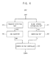
- FIG. 6 is a block diagram illustrating a common voltage controlling group included in a timing controller according to an embodiment of the present inventive concept.
- the timing controller 200 may include a common voltage control group 220'.
- the common voltage control group 220' includes the blank interval determining part 221, the comparing part 222 and the common voltage controller 223.
- the common voltage control group 220' may further include a frequency detecting part 224 and a DVR generator 225.
- the frequency detecting part 224 may detect a driving frequency FREQ of the display panel 100 based on the input control signal CONT.
- the frequency detecting part 224 may output the driving frequency FREQ to the DVR generator 225.
- the frequency detecting part 224 will be explained in detail with reference to FIG. 7 .
- the DVR generator 225 generates a DVR value DVR according to the driving frequency FREQ.
- the DVR value DVR corresponds to a level of the common voltage VCOM.
- the DVR value DVR may determine the first voltage level and the second voltage level.
- the DVR generator 225 may output the DVR value DVR to the common voltage controller 223.
- the DVR generator 225 may be explained in detail with reference to FIG. 8 .
- FIG. 7 is a block diagram illustrating a frequency detecting part included in a timing controller according to an embodiment of the present inventive concept.
- the timing controller 200 may include the oscillator.
- the frequency detecting part 224 may include an oscillation clock counter 224A, a reference value storing part 224B and a frequency determining part 224C.
- the oscillator may generate an oscillation clock OSC CLK.
- the oscillation clock OSC_CLK has a fixed interval.
- the oscillator may output the oscillation clock OSC_CLK to the oscillation clock counter 224A.
- the oscillation clock counter 224A may count the oscillation clock OSC CLK based on the input control signal CONT.
- the oscillation clock counter 224A may generate an input signal count value A based on the counting of the oscillation clock OSC CLK.
- the oscillation clock counter 224A may output the input signal count value A to the frequency determining part 224C.
- the reference value storing part 224B may store a plurality of reference count values REF respectively corresponding to a plurality of driving frequencies.
- the reference value storing part 224B may store the reference count values REF respectively corresponding to 60 Hz, 48 Hz and 40 Hz.
- the reference value storing part 224B may output the reference count values REF to the frequency determining part 224C.
- the frequency determining part 224C may compare the input signal count value A with each of the reference count values REF. The frequency determining part 224C may find a reference count value REF that is substantially the same as or similar to the input signal count value A among the reference count values REF. The frequency determining part 224C may determine the driving frequency FREQ based on the reference count value REF that is substantially the same as or similar to the input signal count value A.
- FIG. 8 is a block diagram illustrating a DVR generator included in a timing controller according to an embodiment of the present inventive concept.
- the DVR generator 225 may include a look-up table 225A.
- the look-up table 225A may store a plurality of DVR values DVR respectively corresponding to a plurality of driving frequencies. For example, the look-up table 225A may store the DVR values DVR respectively corresponding to 60 Hz, 48 Hz and 40 Hz. Each of the DVR values DVR corresponds to a level of the common voltage. Each of the DVR values DVR may determine the first voltage level and the second voltage level.
- the frame masking part may mask at least one frame between the first and second frames based on the input signal.
- the frame masking part may convert the driving frequency FREQ to an ARP driving frequency ARP.
- the frame masking part may convert the driving frequency of 60 Hz to the ARP driving frequency ARP of 30 Hz or 12 Hz.
- the frame masking part may convert the driving frequency of 48 Hz to the ARP driving frequency ARP of 24 Hz or 9.6 Hz.
- the frame masking part may convert the driving frequency of 40 Hz to the ARP driving frequency ARP of 20 Hz or 8 Hz.
- the frame masking part will be explained in detail with reference to FIG. 9 .
- the DVR generator 225 may further include an ARP IP 225B.
- the ARP IP 225B may output the ARP driving frequency ARP to the look-up table 225A.
- the look-up table 225A may find the DVR value DVR corresponding to the driving frequency FREQ and the ARP driving frequency ARP.
- the look-up table 225A may find the DVR value of 66 from LUT1.
- the driving frequency FREQ is 48 Hz, and the ARP driving frequency is 9.6 Hz
- the look-up table 225A may find the DVR value of 62 from LUT2.
- the driving frequency FREQ is 40 Hz
- the ARP driving frequency is 20 Hz
- the look-up table 225A may find the DVR value of 55 from LUT3.
- the DVR generator 225 may output the DVR value DVR to the common voltage controller 223.
- FIG. 9 is a diagram illustrating a method of driving a display apparatus by an FMD method according to an embodiment of the present inventive concept.
- the timing controller 200 may include the frame masking part.
- the frame masking part may mask a frame based on the FMD method.
- the FMD method is not applied to a first image X.
- the first image X may be displayed with k Hz of driving frequency FREQ.
- the k may be one of 60, 48 and 40.
- the first image X includes a first frame 1F and a second frame 2F subsequent to the first frame 1F.
- the first image X includes a first blank interval having a first duration BLK_X between the first frame 1F and the second frame 2F.
- the first image X may further include third, fourth, fifth and sixth frames 3F, 4F, 5F, 6F.
- the blank interval determining part 221 may determine the first duration BLK_X.
- the FMD method is applied to a second image Y.
- the second image Y may be displayed with k/2 Hz of an ARP driving frequency ARP.
- the second image Y includes a first frame 1F and a second frame 2F subsequent to the first frame 1F. One frame is masked between the first frame 1F and the second frame 2F in the second image Y.
- the second image Y includes a second blank interval having a second duration BLK_Y between the first frame 1F and the second frame 2F.
- the second blank interval is extended compared to the first blank interval. In other words, the second blank interval is longer than the first blank interval.
- the second duration BLK_Y is longer than the first duration BLK_X.
- the blank interval determining part 221 may determine the second duration time BLK_Y.
- the ARP IP 225B may output k/2 Hz of an ARP driving frequency ARP to the look-up table 225A.
- the FMD method is applied to a third image Z.
- the third image Z may be displayed with k/5 Hz of an ARP driving frequency ARP.
- the third image Z includes a first frame 1F and a second frame 2F subsequent to the first frame 1F. Four frames are masked between the first frame 1F and the second frame 2F in the third image Z.
- the third image Z includes a third blank interval having a third duration BLK Z between the first frame 1F and the second frame 2F.
- the third blank interval is extended compared to the first and second blank intervals. In other words, the third blank interval is longer than both of the first and second blank intervals.
- the third duration BLK_Z is longer than the first and second durations BLK_X, BLK_Y.
- the blank interval determining part 221 may determine the third duration BLK Z.
- the ARP IP 225B may output k/5 Hz of an ARP driving frequency ARP to the look-up table 225A.
- FIG. 10 is a flow chart illustrating a method of driving a display apparatus according to an embodiment of the present inventive concept.
- a method of driving the display apparatus includes determining the duration BLK of the blank interval between the first and second frames and comparing the duration BLK with the first reference time S100.
- the method may include detecting the driving frequency FREQ S110.
- the method may include comparing the input signal count value A where the oscillation clock OSC_CLK is counted with each of the reference count values REF to detect the driving frequency FREQ.
- the method may include determining the DVR value DVR according to the driving frequency FREQ.
- the DVR value DVR may determine the first voltage level and the second voltage level.
- the common voltage VCOM may be swung between the first voltage level and the second voltage level during the blank interval.
- a swinging amplitude of the common voltage VCOM may be a difference of the first voltage level and the average of the common voltage VCOM.
- the method may include determining the swinging amplitude according to the driving frequency FREQ S120. For example, the method may determine the swinging amplitude considering the ARP driving frequency ARP according to the FMD method.
- the method includes modulating the common voltage VCOM during the blank interval and holding the average of the common voltage VCOM at a fixed level during the blank interval S200.
- the common voltage VCOM may be swung between the first voltage level and the second voltage level during the blank interval.
- the method includes holding the common voltage VCOM at a fixed level S300.
- FIG. 11 is a diagram illustrating operations of a blank interval determining part included in a timing controller according to an embodiment of the present inventive concept.
- the blank interval determining part 221 determines the duration BLK of the blank interval between the first frame and the second frame.
- the blank interval determining part 221 determines a first duration BLK X of a first blank interval between a first frame 1F and a second frame 2F in a first image X.
- the blank interval determining part 221 determines a second duration BLK Y of a second blank interval between a first frame 1F and a second frame 2F in a second image Y.
- the blank interval determining part 221 determines a third duration BLK Z of a third blank interval between a first frame 1F and a second frame 2F in a third image Z.
- the timing controller 200 may include the oscillator.
- the oscillator may generate the oscillation clock OSC_CLK.
- the oscillation clock OSC_CLK has a fixed interval.
- the blank interval determining part 221 may include the oscillation clock counter 221A.
- the oscillation clock counter 221A may count the oscillation clock OSC CLK during the first blank interval in the first image X.
- the oscillation clock counter 221A may determine the first duration BLK_X based on a first number of the oscillation clocks OSC_CLK counted during the first blank interval.
- the oscillation clock counter 221A may count the oscillation clock OSC CLK during the second blank interval in the second image Y.
- the oscillation clock counter 221A may determine the second duration BLK_Y based on a second number of the oscillation clocks OSC CLK counted during the second blank interval.
- the oscillation clock counter 221A may count the oscillation clock OSC CLK during the third blank interval in the third image Z.
- the oscillation clock counter 221A may determine the third duration BLK_Z based on a third number of the oscillation clocks OSC_CLK counted during the third blank interval.
- the comparing part 222 stores a first reference time T1.
- the comparing part 222 compares the first duration BLK_X with the first reference time T1 in the first image X.
- the comparing part 222 determines an order relationship between the first duration BLK_X and the first reference time T1 in the first image X.
- the first duration BLK_X may be shorter than the first reference time T1.
- the comparing part 222 compares the second duration BLK_Y with the first reference time T1 in the second image Y.
- the comparing part 222 determines an order relationship between the second duration BLK_Y and the first reference time T1 in the second image X.
- the second duration BLK_Y may be longer than the first reference time T1.
- the comparing part 222 compares the third duration BLK_Z with the first reference time T1 in the third image Z.
- the comparing part 222 determines an order relationship between the third duration BLK_Z and the first reference time T1 in the third image Z.
- the third duration BLK_Z may be longer than the first reference time T1.
- the comparing part 222 outputs the comparison signal C including a comparison result between the first, second and third duration times BLK X, BLK Y, BLK Z and the first reference time T1 to the common voltage controller 223.
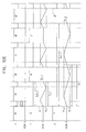
- FIGS. 12A , 12B , 12C and 13 are diagrams illustrating a common voltage outputted from a common voltage generator included in a display apparatus according to an embodiment of the present inventive concept.
- the common voltage controller 223 generates the fourth control signal CONT4 based on the comparison signal C.
- the common voltage generator 600 may generate the common voltage VCOM based on the fourth control signal CONT4.
- the common voltage controller 223 generates the fourth control signal CONT4 for controlling the common voltage VCOM to be modulated and an average of the common voltage VCOM to be fixed during the blank interval when the duration BLK is longer than the first reference time T1 based on the comparison signal C.
- the common voltage generator 600 may generate the common voltage VCOM modulated during the blank interval while the average of the common voltage VCOM is fixed during the blank interval based on the fourth control signal CONT4.
- the common voltage VCOM may also be swung between a first voltage level and a second voltage level during the blank interval.
- the duration BLK may be a multiple of a swinging period of the common voltage VCOM.
- the comparing part 222 may further include a second reference time T2.
- the comparing part 222 may compare the duration BLK with the second reference time T2 when the duration BLK is longer than the first reference time T1.
- the comparing part 222 may determine an order relationship between the duration BLK and the second reference time T2.
- the comparison signal C may further include a comparison result between the duration BLK and the second reference time T2.
- the common voltage controller 223 may generate the fourth control signal CONT4 for controlling the swinging period to be substantially the same as the duration BLK when duration BLK is longer than the first reference time T1 and equal to or shorter than the second reference time T2 based on the comparison signal C.
- the common voltage generator 600 may generate the common voltage VCOM where a swinging period is substantially the same as the duration BLK based on the fourth control signal CONT4.
- the common voltage controller 223 may generate the fourth control signal CONT4 for controlling the swinging period to be substantially the same as the second reference time T2 when duration BLK is longer than the second reference time T2 based on the comparison signal C.
- the common voltage generator 600 may generate the common voltage VCOM where a swinging period is substantially the same as the second reference time T2 based on the fourth control signal CONT4.
- the duration BLK may be a multiple of the second reference time T2.
- the frequency detecting part 224 may detect a driving frequency FREQ of the display panel 100.
- the DVR generator 225 generates the DVR value DVR according to the driving frequency FREQ or the ARP driving frequency ARP.
- the common voltage controller 223 may determine the first voltage level and the second voltage level based on the DVR value DVR.
- the common voltage controller 223 may generate the fourth control signal CONT4 for controlling the common voltage VCOM to be fixed during the blank interval when duration time BLK is equal to or shorter than the first reference time T1 based on the comparison signal C.
- the common voltage generator 600 may generate the common voltage VCOM that is fixed during the blank interval based on the fourth control signal CONT4.
- the first duration BLK_X is equal to or shorter than the first reference time T1 in the first image X.
- the common voltage controller 223 may generate the fourth control signal CONT4 for controlling a first common voltage VCOM_X to be fixed during the first blank interval based on the comparison signal C.
- the common voltage generator 600 may generate the first common voltage VCOM_X that is fixed during first blank interval based on the fourth control signal CONT4.
- the second duration BLK_Y is longer than the first reference time T1 and equal to or shorter than the second reference time T2 in the second image Y.
- the common voltage controller 223 may generate the fourth control signal CONT4 for controlling a second common voltage VCOM_Y to be modulated, an average of the second common voltage VCOM_Y to be fixed during the second blank interval and a second swinging period T_Y of the second common voltage VCOM_Y to be substantially the same as the second duration time BLK_Y based on the comparison signal C.
- the frequency detecting part 224 may detect a driving frequency FREQ of the second image Y.
- the DVR generator 225 may generate the DVR value DVR according to the driving frequency FREQ or an ARP driving frequency ARP of the second image Y.
- the common voltage controller 223 may determine the first voltage level V1_Y and the second voltage level V2_Y based on the DVR value DVR.
- the common voltage generator 600 may generate the second common voltage VCOM_Y that is swung between the first voltage level V1_Y and the second voltage level V2_Y during the second blank interval and that has the second swinging period T_Y substantially the same as the second duration BLK_Y based on the fourth control signal CONT4.
- the third duration BLK_Z is longer than the second reference time T2 in the third image Z.
- the common voltage controller 223 may generate the fourth control signal CONT4 for controlling a third common voltage VCOM_Z to be modulated, an average of the third common voltage VCOM_Z to be fixed during the third blank interval and a third swinging period T_Z of the third common voltage VCOM_Z to be substantially the same as the second reference time T2 based on the comparison signal C.
- the third duration time BLK_Z may be a multiple of the second reference time T2.
- the frequency detecting part 224 may detect a driving frequency FREQ of the third image Z.
- the DVR generator 225 may generate the DVR value DVR according to the driving frequency FREQ or an ARP driving frequency ARP of the third image Z.
- the common voltage controller 223 may determine the first voltage level V1_Z and the second voltage level V2_Z based on the DVR value DVR.
- the common voltage generator 600 may generate the third common voltage VCOM_Z that is swung between the first voltage level V1_Z and the second voltage level V2_Z during the third blank interval and that has the third swinging period T_Z substantially the same as the second reference time T2 based on the fourth control signal CONT4.
- the second common voltage VCOM Y may be modulated and may have a first sine wave during the second blank interval in the second image Y.
- a period of the first sine wave may be substantially the same as the second swinging period T_Y.
- An amplitude P_Y of the first sine wave may be substantially the same as a difference of the first voltage level V1_Y and an average of the second common voltage VCOM_Y.
- the third common voltage VCOM_Z may be modulated and may have a second sine wave during the third blank interval in the third image Z.
- a period of the second sine wave may be substantially the same as the third swinging period T_Z.
- An amplitude P_Z of the second sine wave may be substantially the same as a difference of the first voltage level V1_Z and an average of the third common voltage VCOM_Z.
- a common voltage VCOM is slowly modulated according to a sine wave while an average of the common voltage VCOM is fixed so that flickers caused by a rapid modulation of the common voltage VCOM can be reduced.
- the second common voltage VCOM_Y may be modulated and may have a first triangle wave during the second blank interval in the second image Y.
- a period of the first triangle wave may be substantially the same as the second swinging period T_Y
- An amplitude P_Y of the first triangle wave may be substantially the same as a difference of the first voltage level V1_Y and an average of the second common voltage VCOM_Y.
- the third common voltage VCOM_Z may be modulated and may have a second triangle wave during the third blank interval in the third image Z.
- a period of the second triangle wave may be substantially the same as the third swinging period T_Z.
- An amplitude P_Z of the second triangle wave may be substantially the same as a difference of the first voltage level V1_Z and an average of the third common voltage VCOM_Z.
- a luminance is modulated before beginning of every frame in a first luminance LUM_X of the first image X, a second luminance LUM_Y of the second image Y and a third luminance LUM_Z of the third image Z.
- the blank interval determining part 221 determines the first duration BLK X of the first blank interval between the first frame 1F and the second frame 2F in the first image X.
- the blank interval determining part 221 determines the second duration BLK Y of the second blank interval between the first frame 1F and the second frame 2F in the second image Y.
- the blank interval determining part 221 determines the third duration BLK Z of the third blank interval between the first frame 1F and the second frame 2F in the third image Z.
- the comparing part 222 compares the first duration BLK_X with the first reference time T1 in the first image X.
- the comparing part 222 compares the second duration BLK_Y with the first reference time T1 in the second image Y.
- the comparing part 222 compares the third duration BLK_Z with the first reference time T1 in the third image Z.
- the common voltage generator 600 may apply a plurality of common voltage pulses to the common voltage VCOM with a fixed interval during the blank interval when the duration BLK is longer than the first reference time T1.
- the common voltage generator 600 may hold the common voltage VCOM at a fixed level during the blank interval when the duration BLK is equal to or shorter than the first reference time T1.
- the common voltage generator 600 may hold the first common voltage VCOM_X at a fixed level because the first duration BLK_X is equal to or shorter than the first reference time T1 in the first image X.
- the common voltage generator 600 may apply a plurality of second common voltage pulses to the second common voltage VCOM_Y because the second duration BLK_Y is longer than the first reference time T1.
- the second common voltage pulses may correspond to the pulses of the second luminance LUM_Y so that an interval of the second common voltage pulses is substantially the same as an interval of the pulses of the first luminance LUM_X.
- the common voltage generator 600 may apply a plurality of third common voltage pulses to the third common voltage VCOM_Z because the third duration BLK_Z is longer than the first reference time T1.
- the third common voltage pulses may correspond to the pulses of the third luminance LUM_Z so that an interval of the third common voltage pulses is substantially the same as an interval of the pulses of the first luminance LUM_X.
- a plurality of common voltage pulses is applied to a common voltage in low frequency driving to narrow an interval between each pulse.
- a common voltage is variously modulated during an extended blank interval according to a driving frequency so that flickers and afterimages are reduced.
- display quality of the display panel can be increased.
- a display apparatus and/or a system including the display apparatus, such as a mobile phone, a smart phone, a personal digital assistant (PDA), a portable media player (PMP), a digital camera, a digital television, a set-top box, a music player, a portable game console, a navigation device, a personal computer (PC), a server computer, a workstation, a tablet computer, a laptop computer, a smart card, a printer, etc.
- PDA personal digital assistant
- PMP portable media player
- PC personal computer
- server computer a workstation
- tablet computer a laptop computer
- smart card a printer, etc.
Landscapes
- Engineering & Computer Science (AREA)
- Chemical & Material Sciences (AREA)
- Crystallography & Structural Chemistry (AREA)
- Physics & Mathematics (AREA)
- Computer Hardware Design (AREA)
- General Physics & Mathematics (AREA)
- Theoretical Computer Science (AREA)
- Power Engineering (AREA)
- Control Of Indicators Other Than Cathode Ray Tubes (AREA)
- Liquid Crystal Display Device Control (AREA)
- Liquid Crystal (AREA)
Abstract

Description
- Embodiments of the present inventive concept relate generally to display devices, and more particularly to methods of driving display apparatuses, display apparatuses performing the methods and timing controllers included in the display apparatuses.
- Generally, a liquid crystal display ("LCD") apparatus includes a first substrate including a pixel electrode, a second substrate including a common electrode and a liquid crystal layer disposed between the first substrate and the second substrate. An electric field is generated by voltages applied to the pixel electrode and the common electrode. By adjusting an intensity of the electric field, a transmittance of light passing through the liquid crystal layer may be adjusted so that an image may be displayed.
- A driving frequency may vary according to driving options. For example, since a common voltage may be controlled according to the driving frequency, the driving frequency may be varied to generate an optimum common voltage for reducing flickers and afterimages.
- A Frame Masking Driving ("FMD") method may be used to change the driving frequency. In this method, by masking some frames, blank intervals between frames are extended.
- The present invention sets out to improve the display quality of such a display panel.
- A method of driving a display apparatus according to an embodiment of the present inventive concept includes determining a duration of a blank interval between a first frame and a second frame, wherein the second frame is subsequent to the first frame, and modulating a common voltage during the blank interval when the duration is longer than a first reference time, wherein an average of the common voltage is fixed during the blank interval.
- In an embodiment of the present inventive concept, modulating the common voltage may include swinging the common voltage between a first voltage level and a second voltage level.
- In an embodiment of the present inventive concept, the duration may be a multiple of a swinging period of the modulated common voltage.
- In an embodiment of the present inventive concept, a swinging period of the modulated common voltage may be substantially the same as the duration when the duration is longer than the first reference time and equal to or shorter than a second reference time, and the swinging period may be substantially the same as the second reference time when the duration is longer than the second reference time.
- In an embodiment of the present inventive concept, the duration may be a multiple of the second reference time.
- In an embodiment of the present inventive concept, the method may further include detecting a driving frequency of a display panel, and determining the first and second voltage levels in response to the driving frequency.
- In an embodiment of the present inventive concept, a swinging amplitude of the modulated common voltage may be substantially the same as a difference of the average of the common voltage and the first voltage level.
- In an embodiment of the present inventive concept, detecting the driving frequency may include comparing an input signal count value with a plurality of reference count values, the input signal count value being generated by counting an oscillation clock in response to an input signal.
- In an embodiment of the present inventive concept, determining the first and second voltage levels may include referring to a look-up table where a plurality of first values respectively corresponding to a plurality of driving frequencies is stored.
- In an embodiment of the present inventive concept, modulating the common voltage may include modulating the common voltage to have a sine wave during the blank interval.
- In an embodiment of the present inventive concept, modulating the common voltage may include modulating the common voltage to have a triangle wave during the blank interval.
- In an embodiment of the present inventive concept, determining the duration may include counting oscillation clocks during the blank interval.
- In an embodiment of the present inventive concept, the method may further include masking at least one frame between the first and second frames in response to an input signal to extend the blank interval.
- In an embodiment of the present inventive concept, determining the duration may include determining a duration of the extended blank interval.
- In an embodiment of the present inventive concept, the method may further include holding the common voltage at a fixed level during the blank interval when the duration is equal to or shorter than the first reference time.
- A display apparatus according to an embodiment of the present inventive concept includes a timing controller including a blank interval determining part configured to determine a duration of a blank interval between a first frame and a second frame, wherein the second frame is subsequent to the first frame, a comparing part configured to compare the duration with a first reference time, and a common voltage controller configured to generate a first common voltage control signal when the duration is longer than the first reference time, a common voltage generator configured to generate a first common voltage in response to the first common voltage control signal, the first common voltage being modulated during the blank interval, an average of the common voltage being fixed during the blank interval, and a display panel configured to be driven in response to the first common voltage.
- In an embodiment of the present inventive concept, the first common voltage may be swung between a first voltage level and a second voltage level.
- In an embodiment of the present inventive concept, the duration may be a multiple of a swinging period of the first common voltage.
- In an embodiment of the present inventive concept, the comparing part may be configured to compare the duration with a second reference time, and a swinging period of the first common voltage may be substantially the same as the duration when the duration is longer than the first reference time and equal to or shorter than the second reference time, and the swinging period may be substantially the same as the second reference time when the duration is longer than the second reference time.
- In an embodiment of the present inventive concept, the timing controller may further include a frequency detecting part configured to detect a driving frequency of the display panel and a first generator configured to generate a first value determining the first and second voltage levels in response to the driving frequency.
- In an embodiment of the present inventive concept, the frequency detecting part may include an oscillation clock counter configured to count an oscillation clock in response to an input signal to generate an input signal count value, a reference value storing part configured to store a plurality of reference count values respectively corresponding to a plurality of driving frequencies, and a frequency determining part configured to compare the input signal count value with each of the reference count values to determine the driving frequency of the display panel.
- In an embodiment of the present inventive concept, the first generator may include a look-up table storing a plurality of first values respectively corresponding to a plurality of driving frequencies.
- In an embodiment of the present inventive concept, the first common voltage may be a sine wave modulated during the blank interval.
- In an embodiment of the present inventive concept, the first common voltage may be a triangle wave modulated during the blank interval.
- In an embodiment of the present inventive concept, the blank interval determining part may include an oscillation clock counter configured to count oscillation clocks during the blank interval.
- In an embodiment of the present inventive concept, the display apparatus may further include a frame masking part configured to mask at least one frame between the first and second frames in response to an input signal to extend the blank interval.
- In an embodiment of the present inventive concept, the blank interval determining part may be further configured to determine a duration of the extended blank interval.
- In an embodiment of the present inventive concept, the common voltage controller may be further configured to generate a second common voltage control signal when the duration is equal to or shorter than the first reference time, and the common voltage generator may be further configured to generate a second common voltage in response to the second common voltage control signal, the second common voltage being fixed during the blank interval.
- A timing controller according to an embodiment of the present inventive concept includes a blank interval determining part configured to determine a duration of a blank interval between a first frame and a second frame, wherein the second frame is subsequent to the first frame, a comparing part configured to compare the duration with a first reference time, and a common voltage controller configured to generate a common voltage control signal when the duration is longer than the first reference time, wherein the common voltage control signal controls a common voltage to be modulated and an average of the common voltage to be fixed during the blank interval.
- In an embodiment of the present inventive concept, the common voltage control signal may control the common voltage to be swung between a first voltage level and a second voltage level.
- In an embodiment of the present inventive concept, the blank interval determining part may include an oscillation clock counter configured to count oscillation clocks during the blank interval.
- In an embodiment of the present inventive concept, the timing controller may further include a frame masking part configured to mask at least one frame between the first and second frames in response to an input signal to extend the blank interval.
- At least some of the above and other features of the invention n are set out in the claims.
- The above and other features of the present inventive concept will be made more apparent by describing in detail embodiments thereof with reference to the accompanying drawings, in which:
-
FIG. 1 is a block diagram illustrating a display apparatus according to an embodiment of the present inventive concept; -
FIG. 2 is a block diagram illustrating a timing controller according to an embodiment of the present inventive concept; -
FIG. 3 is a block diagram illustrating a blank interval determining part included in a timing controller according to an embodiment of the present inventive concept; -
FIG. 4 is a flow chart illustrating a method of driving a display apparatus according to an embodiment of the present inventive concept; -
FIG. 5 is a flow chart illustrating a method of modulating a common voltage according to an embodiment of the present inventive concept; -
FIG. 6 is a block diagram illustrating a common voltage controlling group included in a timing controller according to an embodiment of the present inventive concept; -
FIG. 7 is a block diagram illustrating a frequency detecting part included in a timing controller according to an embodiment of the present inventive concept; -
FIG. 8 is a block diagram illustrating a DVR generator included in a timing controller according to an embodiment of the present inventive concept; -
FIG. 9 is a diagram illustrating a method of driving a display apparatus by a Frame Masking Driving method according to an embodiment of the present inventive concept; -
FIG. 10 is a flow chart illustrating a method of driving a display apparatus according to an embodiment of the present inventive concept; -
FIG. 11 is a diagram illustrating operations of a blank interval determining part included in a timing controller according to an embodiment of the present inventive concept; -
FIGS. 12A ,12B ,12C and13 are diagrams illustrating a common voltage outputted from a common voltage generator included in a display apparatus according to an embodiment of the present inventive concept. - Hereinafter, embodiments of the present inventive concept will be explained in detail with reference to the accompanying drawings.
-
FIG. 1 is a block diagram illustrating a display apparatus according to an embodiment of the present inventive concept. - Referring to
FIG. 1 , the display apparatus includes adisplay panel 100 and a panel driver. The panel driver includes atiming controller 200, agate driver 300, a gammareference voltage generator 400, adata driver 500 and acommon voltage generator 600. The elements of the display apparatus may be composed of circuits. - The
display panel 100 includes a display region for displaying an image and a peripheral region adjacent to the display region. - The
display panel 100 includes a plurality of gate lines GL, a plurality of data lines DL and a plurality of pixels electrically connected to the gate lines GL and the data lines DL. The gate lines GL extend in a first direction D1 and the data lines DL extend in a second direction D2 crossing the first direction D1. - In an embodiment of the present inventive concept, each of the pixels may include a switching element, a liquid crystal capacitor and a storage capacitor. The liquid crystal capacitor and the storage capacitor may be electrically connected to the switching element. The pixels may be arranged in a matrix configuration.
- The
timing controller 200 receives input image data RGB and an input control signal CONT from an external device. The input image data RGB may include red image data R, green image data G and blue image data B. The input control signal CONT may include a master clock signal and a data enable signal. The input control signal CONT may further include a vertical synchronizing signal and a horizontal synchronizing signal. - The
timing controller 200 generates a first control signal CONT1, a second control signal CONT2, a third control signal CONT3, a fourth control signal CONT4 and a data signal DAT based on the input image data RGB and the input control signal CONT. - The
timing controller 200 generates the first control signal CONT1 for controlling operations of thegate driver 300 based on the input control signal CONT, and outputs the first control signal CONT1 to thegate driver 300. The first control signal CONT1 may include a vertical start signal and a gate clock signal. - The
timing controller 200 generates the second control signal CONT2 for controlling operations of thedata driver 500 based on the input control signal CONT, and outputs the second control signal CONT2 to thedata driver 500. The second control signal CONT2 may include a horizontal start signal and a load signal. - The
timing controller 200 generates the data signal DAT based on the input image data RGB. Thetiming controller 200 outputs the data signal DAT to thedata driver 500. The data signal DAT may be substantially the same as the input image data RGB or the data signal DAT may be compensated image data generated by compensating the input image data RGB. For example, thetiming controller 200 may selectively perform an image quality compensation, a spot compensation, an adaptive color correction (ACC), and/or a dynamic capacitance compensation (DCC) on the input image data RGB to generate the data signal DAT. - The
timing controller 200 generates the third control signal CONT3 for controlling operations of the gammareference voltage generator 400 based on the input control signal CONT, and outputs the third control signal CONT3 to the gammareference voltage generator 400. - The
timing controller 200 generates the fourth control signal CONT4 for controlling operations of thecommon voltage generator 600 based on the input control signal CONT, and outputs the fourth control signal CONT4 to thecommon voltage generator 600. - The
timing controller 200 will be explained in detail with reference toFIG. 2 . - The
gate driver 300 generates gate signals for driving the gate lines GL in response to the first control signal CONT1 provided from thetiming controller 200. Thegate driver 300 sequentially outputs the gate signals to the gate lines GL. - In an embodiment of the present inventive concept, the
gate driver 300 may be directly mounted on thedisplay panel 100, or may be connected to thedisplay panel 100 as a tape carrier package (TCP) type. In addition, thegate driver 300 may be integrated on the peripheral region of thedisplay panel 100. - The gamma
reference voltage generator 400 generates a gamma reference voltage VGREF in response to the third control signal CONT3 provided from thetiming controller 200. The gammareference voltage generator 400 outputs the gamma reference voltage VGREF to thedata driver 500. The level of the gamma reference voltage VGREF corresponds to grayscales of a plurality of pixel data included in the data signal DAT. - In an embodiment of the present inventive concept, the gamma
reference voltage generator 400 may be disposed in thetiming controller 200, or may be disposed in thedata driver 500. - The
data driver 500 receives the second control signal CONT2 and the data signal DAT from thetiming controller 200, and receives the gamma reference voltage VGREF from the gammareference voltage generator 400. Thedata driver 500 converts the data signal DAT to data voltages having analog levels based on the gamma reference voltage VGREF. Thedata driver 500 outputs the data voltages to the data lines DL. - In an embodiment of the present inventive concept, the
data driver 500 may be directly mounted on thedisplay panel 100, or may be connected to thedisplay panel 100 as a TCP type. In addition, thedata driver 500 may be integrated on the peripheral region of thedisplay panel 100. - The
common voltage generator 600 generates a common voltage VCOM in response to the fourth control signal CONT4 provided from thetiming controller 200. Thecommon voltage generator 600 outputs the common voltage VCOM to thedisplay panel 100. - The
common voltage generator 600 and the common voltage VCOM will be explained in detail with reference toFIGS. 2 ,4 ,5 ,10 ,12A ,12B ,12C and13 . -
FIG. 2 is a block diagram illustrating a timing controller according to an embodiment of the present inventive concept. - Referring to
FIGS. 1 and2 , thetiming controller 200 includes acontrol signal generator 210, a commonvoltage control group 220 and adata signal generator 230. The commonvoltage control group 220 includes a blankinterval determining part 221, a comparingpart 222 and acommon voltage controller 223. - The
control signal generator 210 generates the first through third control signals CONT1, CONT2, CONT3 based on the input control signal CONT. Thecontrol signal generator 210 outputs the first control signal CONT1 to thegate driver 300. Thecontrol signal generator 210 outputs the second control signal CONT2 to thedata driver 500. Thecontrol signal generator 210 outputs the third control signal CONT3 to the gammareference voltage generator 400. - The blank
interval determining part 221 determines a duration BLK of a blank interval between a first frame and a second frame subsequent to the first frame. The blank interval may be a vertical blank interval between the first and second frames. The blank interval may be an extended blank interval including a frame masked by a Frame Masking Driving ("FMD") method. The blankinterval determining part 221 outputs the duration BLK to the comparingpart 222. - The
timing controller 200 may further include an oscillator. The blankinterval determining part 221 may include an oscillation clock counter. - The blank
interval determining part 221 will be explained in detail with reference toFIG. 3 . The FMD method will be explained in detail with reference toFIG. 9 . - The comparing
part 222 stores a first reference time. The comparingpart 222 compares the duration BLK with the first reference time. The comparingpart 222 determines an order relationship between the duration BLK and the first reference time. The comparingpart 222 outputs a comparison signal C to thecommon voltage controller 223. The comparison signal C includes a comparison result between the duration BLK and the first reference time. - The comparing
part 222 may further store a second reference time. The comparingpart 222 may further compare the duration BLK with the second reference time. The comparingpart 222 may further determine an order relationship between the duration BLK and the second reference time. The comparison signal C may further include a comparison result between the duration BLK and the second reference time. - The
common voltage controller 223 generates the fourth control signal CONT4 based on the comparison signal C. The fourth control signal CONT4 controls the common voltage VCOM to be modulated and an average of the common voltage VCOM to be fixed during the blank interval when the duration BLK is longer than the first reference time. The fourth control signal CONT4 may control the common voltage VCOM to be fixed during the blank interval when the duration BLK is equal to or shorter than the first reference time. Thecommon voltage controller 223 outputs the fourth control signal CONT4 to thecommon voltage generator 600. - The
common voltage generator 600 generates a common voltage VCOM based on the fourth control signal CONT4. The common voltage VCOM is modulated during the blank interval while an average of the common voltage VCOM is fixed during the blank interval when the duration BLK is longer than the first reference time. For example, the common voltage VCOM may be swung between a first voltage level and a second voltage level during the blank interval. The common voltage VCOM may be fixed during the blank interval when the duration BLK is equal to or shorter than the first reference time. Thecommon voltage generator 600 outputs the common voltage VCOM to thedisplay panel 100. - The data signal
generator 230 generates the data signal DAT based on the input image data RGB. The data signalgenerator 230 outputs the data signal DAT to thedata driver 500. - The
timing controller 200 may further include a frame masking part. The frame masking part may mask at least one frame between the first and second frames based on the input signal. For example, the frame masking part may mask one frame. In addition, the frame masking part may mask a plurality of frames. The blank interval between the first and second frames may be extended by the masking. For example, the blankinterval determining part 221 may determine the extended blank interval. -
FIG. 3 is a block diagram illustrating a blank interval determining part included in a timing controller according to an embodiment of the present inventive concept. - Referring to
FIGS. 2 and3 , thetiming controller 200 may include the oscillator. The blankinterval determining part 221 may include an oscillation clock counter 221A. - The oscillator may generate an oscillation clock OSC CLK. The oscillation clock OSC CLK has a fixed interval. The oscillator may output the oscillation clock OSC CLK to the oscillation clock counter 221A.
- The oscillation clock counter 221A may count the oscillation clock OSC_CLK during the blank interval based on the input control signal CONT. The oscillation clock counter 221A may determine the duration BLK of the blank interval based on the number of counted oscillation clocks OSC_CLK.
-
FIG. 4 is a flow chart illustrating a method of driving a display apparatus according to an embodiment of the present inventive concept. - Referring to
FIGS. 1 through 4 , a method of driving the display apparatus includes determining the duration BLK of the blank interval between the first and second frames and comparing the duration BLK with the first reference time S100. - When the duration BLK is longer than the first reference time, the method includes modulating the common voltage VCOM during the blank interval and holding the average of the common voltage VCOM at a fixed level during the blank interval S200. For example, the common voltage VCOM may be swung between the first voltage level and the second voltage level during the blank interval.
- When the duration BLK is equal to or shorter than the first reference time, the method includes holding the common voltage VCOM at a fixed level S300.
-
FIG. 5 is a flow chart illustrating a method of modulating a common voltage according to an embodiment of the present inventive concept. - Referring to
FIGS. 1 through 5 , the method of driving the display apparatus includes comparing the duration BLK with the second reference time when the duration BLK is longer than the first reference time S210. - The common voltage VCOM may be swung between the first voltage level and the second voltage level during the blank interval when the duration BLK is longer than the first reference time S210. In this case, the duration BLK may be a multiple of a swinging period of the common voltage VCOM.
- When the duration BLK is longer than the second reference time, the swinging period of the common voltage VCOM may be substantially the same as the second reference time S220. In this case, the duration BLK may be a multiple of the second reference time.
- When the duration BLK is equal to or shorter than the second reference time, the swinging period of the common voltage VCOM may be substantially the same as the duration BLK S230.
-
FIG. 6 is a block diagram illustrating a common voltage controlling group included in a timing controller according to an embodiment of the present inventive concept. - Referring to
FIGS. 1 ,2 and6 , thetiming controller 200 may include a common voltage control group 220'. - The common voltage control group 220' includes the blank
interval determining part 221, the comparingpart 222 and thecommon voltage controller 223. The common voltage control group 220' may further include afrequency detecting part 224 and aDVR generator 225. - Any repetitive explanation concerning the blank
interval determining part 221 and the comparingpart 222 will be omitted. - The
frequency detecting part 224 may detect a driving frequency FREQ of thedisplay panel 100 based on the input control signal CONT. Thefrequency detecting part 224 may output the driving frequency FREQ to theDVR generator 225. - The
frequency detecting part 224 will be explained in detail with reference toFIG. 7 . - The
DVR generator 225 generates a DVR value DVR according to the driving frequency FREQ. The DVR value DVR corresponds to a level of the common voltage VCOM. The DVR value DVR may determine the first voltage level and the second voltage level. TheDVR generator 225 may output the DVR value DVR to thecommon voltage controller 223. - The
DVR generator 225 may be explained in detail with reference toFIG. 8 . -
FIG. 7 is a block diagram illustrating a frequency detecting part included in a timing controller according to an embodiment of the present inventive concept. - Referring to
FIGS. 2 ,6 and7 , thetiming controller 200 may include the oscillator. Thefrequency detecting part 224 may include an oscillation clock counter 224A, a reference value storing part 224B and a frequency determining part 224C. - The oscillator may generate an oscillation clock OSC CLK. The oscillation clock OSC_CLK has a fixed interval. The oscillator may output the oscillation clock OSC_CLK to the oscillation clock counter 224A.
- The oscillation clock counter 224A may count the oscillation clock OSC CLK based on the input control signal CONT. The oscillation clock counter 224A may generate an input signal count value A based on the counting of the oscillation clock OSC CLK. The oscillation clock counter 224A may output the input signal count value A to the frequency determining part 224C.
- The reference value storing part 224B may store a plurality of reference count values REF respectively corresponding to a plurality of driving frequencies. For example, the reference value storing part 224B may store the reference count values REF respectively corresponding to 60 Hz, 48 Hz and 40 Hz. The reference value storing part 224B may output the reference count values REF to the frequency determining part 224C.
- The frequency determining part 224C may compare the input signal count value A with each of the reference count values REF. The frequency determining part 224C may find a reference count value REF that is substantially the same as or similar to the input signal count value A among the reference count values REF. The frequency determining part 224C may determine the driving frequency FREQ based on the reference count value REF that is substantially the same as or similar to the input signal count value A.
-
FIG. 8 is a block diagram illustrating a DVR generator included in a timing controller according to an embodiment of the present inventive concept. - Referring to
FIGS. 2 ,6 and8 , theDVR generator 225 may include a look-up table 225A. - The look-up table 225A may store a plurality of DVR values DVR respectively corresponding to a plurality of driving frequencies. For example, the look-up table 225A may store the DVR values DVR respectively corresponding to 60 Hz, 48 Hz and 40 Hz. Each of the DVR values DVR corresponds to a level of the common voltage. Each of the DVR values DVR may determine the first voltage level and the second voltage level.
- The frame masking part may mask at least one frame between the first and second frames based on the input signal. The frame masking part may convert the driving frequency FREQ to an ARP driving frequency ARP. For example, the frame masking part may convert the driving frequency of 60 Hz to the ARP driving frequency ARP of 30 Hz or 12 Hz. The frame masking part may convert the driving frequency of 48 Hz to the ARP driving frequency ARP of 24 Hz or 9.6 Hz. The frame masking part may convert the driving frequency of 40 Hz to the ARP driving frequency ARP of 20 Hz or 8 Hz.
- The frame masking part will be explained in detail with reference to
FIG. 9 . - The
DVR generator 225 may further include an ARP IP 225B. The ARP IP 225B may output the ARP driving frequency ARP to the look-up table 225A. For example, the look-up table 225A may find the DVR value DVR corresponding to the driving frequency FREQ and the ARP driving frequency ARP. For example, when the driving frequency FREQ is 60 Hz, and the ARP driving frequency is 30 Hz, the look-up table 225A may find the DVR value of 66 from LUT1. When the driving frequency FREQ is 48 Hz, and the ARP driving frequency is 9.6 Hz, the look-up table 225A may find the DVR value of 62 from LUT2. When the driving frequency FREQ is 40 Hz, and the ARP driving frequency is 20 Hz, the look-up table 225A may find the DVR value of 55 from LUT3. - The
DVR generator 225 may output the DVR value DVR to thecommon voltage controller 223. -
FIG. 9 is a diagram illustrating a method of driving a display apparatus by an FMD method according to an embodiment of the present inventive concept. - Referring to
FIGS. 2 ,6 ,8 and9 , thetiming controller 200 may include the frame masking part. The frame masking part may mask a frame based on the FMD method. - The FMD method is not applied to a first image X. The first image X may be displayed with k Hz of driving frequency FREQ. The k may be one of 60, 48 and 40. The first image X includes a
first frame 1F and asecond frame 2F subsequent to thefirst frame 1F. The first image X includes a first blank interval having a first duration BLK_X between thefirst frame 1F and thesecond frame 2F. The first image X may further include third, fourth, fifth andsixth frames interval determining part 221 may determine the first duration BLK_X. - The FMD method is applied to a second image Y. The second image Y may be displayed with k/2 Hz of an ARP driving frequency ARP. The second image Y includes a
first frame 1F and asecond frame 2F subsequent to thefirst frame 1F. One frame is masked between thefirst frame 1F and thesecond frame 2F in the second image Y. The second image Y includes a second blank interval having a second duration BLK_Y between thefirst frame 1F and thesecond frame 2F. The second blank interval is extended compared to the first blank interval. In other words, the second blank interval is longer than the first blank interval. The second duration BLK_Y is longer than the first duration BLK_X. For example, the blankinterval determining part 221 may determine the second duration time BLK_Y. The ARP IP 225B may output k/2 Hz of an ARP driving frequency ARP to the look-up table 225A. - The FMD method is applied to a third image Z. The third image Z may be displayed with k/5 Hz of an ARP driving frequency ARP. The third image Z includes a
first frame 1F and asecond frame 2F subsequent to thefirst frame 1F. Four frames are masked between thefirst frame 1F and thesecond frame 2F in the third image Z. The third image Z includes a third blank interval having a third duration BLK Z between thefirst frame 1F and thesecond frame 2F. The third blank interval is extended compared to the first and second blank intervals. In other words, the third blank interval is longer than both of the first and second blank intervals. The third duration BLK_Z is longer than the first and second durations BLK_X, BLK_Y. For example, the blankinterval determining part 221 may determine the third duration BLK Z. The ARP IP 225B may output k/5 Hz of an ARP driving frequency ARP to the look-up table 225A. - Hereinafter, embodiments of the present inventive concept will be explained based on images where the FMD method is applied with reference to
FIGS. 11 ,12A through 12C and 13 . However, the embodiments of the present inventive concept are not limited to the FMD method. -
FIG. 10 is a flow chart illustrating a method of driving a display apparatus according to an embodiment of the present inventive concept. - Referring to
FIGS. 1 ,2 ,6 through 8 and 10 , a method of driving the display apparatus includes determining the duration BLK of the blank interval between the first and second frames and comparing the duration BLK with the first reference time S100. - When the duration BLK is longer than the first reference time, the method may include detecting the driving frequency FREQ S110. For example, the method may include comparing the input signal count value A where the oscillation clock OSC_CLK is counted with each of the reference count values REF to detect the driving frequency FREQ.
- The method may include determining the DVR value DVR according to the driving frequency FREQ. The DVR value DVR may determine the first voltage level and the second voltage level. The common voltage VCOM may be swung between the first voltage level and the second voltage level during the blank interval. A swinging amplitude of the common voltage VCOM may be a difference of the first voltage level and the average of the common voltage VCOM. The method may include determining the swinging amplitude according to the driving frequency FREQ S120. For example, the method may determine the swinging amplitude considering the ARP driving frequency ARP according to the FMD method.
- The method includes modulating the common voltage VCOM during the blank interval and holding the average of the common voltage VCOM at a fixed level during the blank interval S200. For example, the common voltage VCOM may be swung between the first voltage level and the second voltage level during the blank interval.
- When the duration BLK is equal to or shorter than the first reference time, the method includes holding the common voltage VCOM at a fixed level S300.
-
FIG. 11 is a diagram illustrating operations of a blank interval determining part included in a timing controller according to an embodiment of the present inventive concept. - Referring to
FIGS. 2 ,3 and11 , the blankinterval determining part 221 determines the duration BLK of the blank interval between the first frame and the second frame. The blankinterval determining part 221 determines a first duration BLK X of a first blank interval between afirst frame 1F and asecond frame 2F in a first image X. The blankinterval determining part 221 determines a second duration BLK Y of a second blank interval between afirst frame 1F and asecond frame 2F in a second image Y. The blankinterval determining part 221 determines a third duration BLK Z of a third blank interval between afirst frame 1F and asecond frame 2F in a third image Z. - The
timing controller 200 may include the oscillator. The oscillator may generate the oscillation clock OSC_CLK. The oscillation clock OSC_CLK has a fixed interval. - The blank
interval determining part 221 may include the oscillation clock counter 221A. The oscillation clock counter 221A may count the oscillation clock OSC CLK during the first blank interval in the first image X. The oscillation clock counter 221A may determine the first duration BLK_X based on a first number of the oscillation clocks OSC_CLK counted during the first blank interval. The oscillation clock counter 221A may count the oscillation clock OSC CLK during the second blank interval in the second image Y. The oscillation clock counter 221A may determine the second duration BLK_Y based on a second number of the oscillation clocks OSC CLK counted during the second blank interval. The oscillation clock counter 221A may count the oscillation clock OSC CLK during the third blank interval in the third image Z. The oscillation clock counter 221A may determine the third duration BLK_Z based on a third number of the oscillation clocks OSC_CLK counted during the third blank interval. - The comparing
part 222 stores a first reference time T1. The comparingpart 222 compares the first duration BLK_X with the first reference time T1 in the first image X. The comparingpart 222 determines an order relationship between the first duration BLK_X and the first reference time T1 in the first image X. For example, the first duration BLK_X may be shorter than the first reference time T1. The comparingpart 222 compares the second duration BLK_Y with the first reference time T1 in the second image Y. The comparingpart 222 determines an order relationship between the second duration BLK_Y and the first reference time T1 in the second image X. For example, the second duration BLK_Y may be longer than the first reference time T1. The comparingpart 222 compares the third duration BLK_Z with the first reference time T1 in the third image Z. The comparingpart 222 determines an order relationship between the third duration BLK_Z and the first reference time T1 in the third image Z. For example, the third duration BLK_Z may be longer than the first reference time T1. The comparingpart 222 outputs the comparison signal C including a comparison result between the first, second and third duration times BLK X, BLK Y, BLK Z and the first reference time T1 to thecommon voltage controller 223. -
FIGS. 12A ,12B ,12C and13 are diagrams illustrating a common voltage outputted from a common voltage generator included in a display apparatus according to an embodiment of the present inventive concept. - Referring to
FIGS. 1 ,2 ,6 ,11 and12A , thecommon voltage controller 223 generates the fourth control signal CONT4 based on the comparison signal C. Thecommon voltage generator 600 may generate the common voltage VCOM based on the fourth control signal CONT4. - The
common voltage controller 223 generates the fourth control signal CONT4 for controlling the common voltage VCOM to be modulated and an average of the common voltage VCOM to be fixed during the blank interval when the duration BLK is longer than the first reference time T1 based on the comparison signal C. For example, thecommon voltage generator 600 may generate the common voltage VCOM modulated during the blank interval while the average of the common voltage VCOM is fixed during the blank interval based on the fourth control signal CONT4. The common voltage VCOM may also be swung between a first voltage level and a second voltage level during the blank interval. For example, the duration BLK may be a multiple of a swinging period of the common voltage VCOM. - The comparing
part 222 may further include a second reference time T2. The comparingpart 222 may compare the duration BLK with the second reference time T2 when the duration BLK is longer than the first reference time T1. The comparingpart 222 may determine an order relationship between the duration BLK and the second reference time T2. The comparison signal C may further include a comparison result between the duration BLK and the second reference time T2. - The
common voltage controller 223 may generate the fourth control signal CONT4 for controlling the swinging period to be substantially the same as the duration BLK when duration BLK is longer than the first reference time T1 and equal to or shorter than the second reference time T2 based on the comparison signal C. For example, thecommon voltage generator 600 may generate the common voltage VCOM where a swinging period is substantially the same as the duration BLK based on the fourth control signal CONT4. - The
common voltage controller 223 may generate the fourth control signal CONT4 for controlling the swinging period to be substantially the same as the second reference time T2 when duration BLK is longer than the second reference time T2 based on the comparison signal C. For example, thecommon voltage generator 600 may generate the common voltage VCOM where a swinging period is substantially the same as the second reference time T2 based on the fourth control signal CONT4. For example, the duration BLK may be a multiple of the second reference time T2. - The
frequency detecting part 224 may detect a driving frequency FREQ of thedisplay panel 100. TheDVR generator 225 generates the DVR value DVR according to the driving frequency FREQ or the ARP driving frequency ARP. Thecommon voltage controller 223 may determine the first voltage level and the second voltage level based on the DVR value DVR. - The
common voltage controller 223 may generate the fourth control signal CONT4 for controlling the common voltage VCOM to be fixed during the blank interval when duration time BLK is equal to or shorter than the first reference time T1 based on the comparison signal C. For example, thecommon voltage generator 600 may generate the common voltage VCOM that is fixed during the blank interval based on the fourth control signal CONT4. - As an example case, the first duration BLK_X is equal to or shorter than the first reference time T1 in the first image X. In this case, the
common voltage controller 223 may generate the fourth control signal CONT4 for controlling a first common voltage VCOM_X to be fixed during the first blank interval based on the comparison signal C. In this case, thecommon voltage generator 600 may generate the first common voltage VCOM_X that is fixed during first blank interval based on the fourth control signal CONT4. - As an example case, the second duration BLK_Y is longer than the first reference time T1 and equal to or shorter than the second reference time T2 in the second image Y. In this case, the
common voltage controller 223 may generate the fourth control signal CONT4 for controlling a second common voltage VCOM_Y to be modulated, an average of the second common voltage VCOM_Y to be fixed during the second blank interval and a second swinging period T_Y of the second common voltage VCOM_Y to be substantially the same as the second duration time BLK_Y based on the comparison signal C. In this case, thefrequency detecting part 224 may detect a driving frequency FREQ of the second image Y. TheDVR generator 225 may generate the DVR value DVR according to the driving frequency FREQ or an ARP driving frequency ARP of the second image Y. Thecommon voltage controller 223 may determine the first voltage level V1_Y and the second voltage level V2_Y based on the DVR value DVR. In this case, thecommon voltage generator 600 may generate the second common voltage VCOM_Y that is swung between the first voltage level V1_Y and the second voltage level V2_Y during the second blank interval and that has the second swinging period T_Y substantially the same as the second duration BLK_Y based on the fourth control signal CONT4. - As an example case, the third duration BLK_Z is longer than the second reference time T2 in the third image Z. In this case, the
common voltage controller 223 may generate the fourth control signal CONT4 for controlling a third common voltage VCOM_Z to be modulated, an average of the third common voltage VCOM_Z to be fixed during the third blank interval and a third swinging period T_Z of the third common voltage VCOM_Z to be substantially the same as the second reference time T2 based on the comparison signal C. In this case, the third duration time BLK_Z may be a multiple of the second reference time T2. In this case, thefrequency detecting part 224 may detect a driving frequency FREQ of the third image Z. TheDVR generator 225 may generate the DVR value DVR according to the driving frequency FREQ or an ARP driving frequency ARP of the third image Z. Thecommon voltage controller 223 may determine the first voltage level V1_Z and the second voltage level V2_Z based on the DVR value DVR. In this case, thecommon voltage generator 600 may generate the third common voltage VCOM_Z that is swung between the first voltage level V1_Z and the second voltage level V2_Z during the third blank interval and that has the third swinging period T_Z substantially the same as the second reference time T2 based on the fourth control signal CONT4. - Referring to
FIGS. 12A and12B , the second common voltage VCOM Y may be modulated and may have a first sine wave during the second blank interval in the second image Y. A period of the first sine wave may be substantially the same as the second swinging period T_Y. An amplitude P_Y of the first sine wave may be substantially the same as a difference of the first voltage level V1_Y and an average of the second common voltage VCOM_Y. - The third common voltage VCOM_Z may be modulated and may have a second sine wave during the third blank interval in the third image Z. A period of the second sine wave may be substantially the same as the third swinging period T_Z. An amplitude P_Z of the second sine wave may be substantially the same as a difference of the first voltage level V1_Z and an average of the third common voltage VCOM_Z.
- According to the present embodiment, a common voltage VCOM is slowly modulated according to a sine wave while an average of the common voltage VCOM is fixed so that flickers caused by a rapid modulation of the common voltage VCOM can be reduced.
- Referring to
FIGS. 12A and12C , the second common voltage VCOM_Y may be modulated and may have a first triangle wave during the second blank interval in the second image Y. A period of the first triangle wave may be substantially the same as the second swinging period T_Y An amplitude P_Y of the first triangle wave may be substantially the same as a difference of the first voltage level V1_Y and an average of the second common voltage VCOM_Y. - The third common voltage VCOM_Z may be modulated and may have a second triangle wave during the third blank interval in the third image Z. A period of the second triangle wave may be substantially the same as the third swinging period T_Z. An amplitude P_Z of the second triangle wave may be substantially the same as a difference of the first voltage level V1_Z and an average of the third common voltage VCOM_Z.
- Referring to
FIGS. 1 ,2 ,11 and13 , a luminance is modulated before beginning of every frame in a first luminance LUM_X of the first image X, a second luminance LUM_Y of the second image Y and a third luminance LUM_Z of the third image Z. - The blank
interval determining part 221 determines the first duration BLK X of the first blank interval between thefirst frame 1F and thesecond frame 2F in the first image X. The blankinterval determining part 221 determines the second duration BLK Y of the second blank interval between thefirst frame 1F and thesecond frame 2F in the second image Y. The blankinterval determining part 221 determines the third duration BLK Z of the third blank interval between thefirst frame 1F and thesecond frame 2F in the third image Z. - The comparing
part 222 compares the first duration BLK_X with the first reference time T1 in the first image X. The comparingpart 222 compares the second duration BLK_Y with the first reference time T1 in the second image Y. The comparingpart 222 compares the third duration BLK_Z with the first reference time T1 in the third image Z. - The
common voltage generator 600 may apply a plurality of common voltage pulses to the common voltage VCOM with a fixed interval during the blank interval when the duration BLK is longer than the first reference time T1. Thecommon voltage generator 600 may hold the common voltage VCOM at a fixed level during the blank interval when the duration BLK is equal to or shorter than the first reference time T1. - For example, the
common voltage generator 600 may hold the first common voltage VCOM_X at a fixed level because the first duration BLK_X is equal to or shorter than the first reference time T1 in the first image X. - For example, the
common voltage generator 600 may apply a plurality of second common voltage pulses to the second common voltage VCOM_Y because the second duration BLK_Y is longer than the first reference time T1. For example, the second common voltage pulses may correspond to the pulses of the second luminance LUM_Y so that an interval of the second common voltage pulses is substantially the same as an interval of the pulses of the first luminance LUM_X. - For example, the
common voltage generator 600 may apply a plurality of third common voltage pulses to the third common voltage VCOM_Z because the third duration BLK_Z is longer than the first reference time T1. For example, the third common voltage pulses may correspond to the pulses of the third luminance LUM_Z so that an interval of the third common voltage pulses is substantially the same as an interval of the pulses of the first luminance LUM_X. - According to the present embodiment of the invention, a plurality of common voltage pulses is applied to a common voltage in low frequency driving to narrow an interval between each pulse.
- In the above described embodiments of the present inventive concept, a common voltage is variously modulated during an extended blank interval according to a driving frequency so that flickers and afterimages are reduced. Thus, display quality of the display panel can be increased.
- The above described embodiments of the present inventive concept may be used in a display apparatus and/or a system including the display apparatus, such as a mobile phone, a smart phone, a personal digital assistant (PDA), a portable media player (PMP), a digital camera, a digital television, a set-top box, a music player, a portable game console, a navigation device, a personal computer (PC), a server computer, a workstation, a tablet computer, a laptop computer, a smart card, a printer, etc.
- While the present inventive concept has been particularly shown and described with reference to embodiments thereof, it will be apparent to those of ordinary skill in the art that various changes in form and detail may be made thereto without departing from the scope of the present inventive concept as defined by the following claims.
Claims (15)
- A method of driving a display apparatus, the method comprising:determining a duration of a blank interval between a first frame and a second frame, wherein the second frame is subsequent to the first frame; andmodulating a common voltage during the blank interval when the duration is longer than a first reference time, wherein an average of the common voltage is fixed during the blank interval.
- A method according to claim 1, wherein modulating the common voltage comprises:swinging the common voltage between a first voltage level and a second voltage level.
- A method according to claim 2, wherein the duration is a multiple of a swinging period of the modulated common voltage.
- A method according to claim 2, wherein a swinging period of the modulated common voltage is substantially the same as the duration when the duration is longer than the first reference time and equal to or shorter than a second reference time, and
wherein the swinging period is substantially the same as the second reference time when the duration is longer than the second reference time. - A method according to claim 4, wherein the duration is a multiple of the second reference time.
- A method according to claim 2, further comprising:detecting a driving frequency of a display panel; anddetermining the first and second voltage levels in response to the driving frequency.
- A method according to claim 6, wherein a swinging amplitude of the modulated common voltage is substantially the same as a difference of the average of the common voltage and the first voltage level.
- A method according to claim 6 or 7, wherein detecting the driving frequency comprises:comparing an input signal count value with a plurality of reference count values, wherein the input signal count value is generated by counting an oscillation clock in response to an input signal.
- A method according to claim 6, 7 or 8, wherein determining the first and second voltage levels comprises:referring to a look-up table where a plurality of first values respectively corresponding to a plurality of driving frequencies is stored.
- A method according to claim 1, wherein modulating the common voltage comprises:modulating the common voltage to have a sine wave during the blank interval.
- A method according to claim 1, wherein modulating the common voltage comprises:modulating the common voltage to have a triangle wave during the blank interval.
- A method according to any preceding claim, wherein determining the duration comprises:counting oscillation clocks during the blank interval.
- A method according to claim 1, further comprising:masking at least one frame between the first and second frames in response to an input signal to extend the blank interval.
- A method of claim 13, wherein determining the duration comprises:determining a duration of the extended blank interval.
- A method according to any preceding claim, further comprising:holding the common voltage at a fixed level during the blank interval when the duration is equal to or shorter than the first reference time.
Applications Claiming Priority (1)
| Application Number | Priority Date | Filing Date | Title |
|---|---|---|---|
| KR1020160004962A KR102513819B1 (en) | 2016-01-14 | 2016-01-14 | Method of driving display apparatus, display apparatus performing the same and timing controller included in the display apparatus |
Publications (2)
| Publication Number | Publication Date |
|---|---|
| EP3193324A2 true EP3193324A2 (en) | 2017-07-19 |
| EP3193324A3 EP3193324A3 (en) | 2017-08-16 |
Family
ID=56939949
Family Applications (1)
| Application Number | Title | Priority Date | Filing Date |
|---|---|---|---|
| EP16189227.8A Withdrawn EP3193324A3 (en) | 2016-01-14 | 2016-09-16 | Method of driving a display apparatus, a display apparatus performing the same and a timing controller included in the display apparatus |
Country Status (4)
| Country | Link |
|---|---|
| US (1) | US10127882B2 (en) |
| EP (1) | EP3193324A3 (en) |
| KR (1) | KR102513819B1 (en) |
| CN (1) | CN106971694B (en) |
Cited By (1)
| Publication number | Priority date | Publication date | Assignee | Title |
|---|---|---|---|---|
| EP3514787A1 (en) * | 2018-01-19 | 2019-07-24 | Samsung Display Co., Ltd. | Sink device and liquid crystal display device including the same |
Families Citing this family (13)
| Publication number | Priority date | Publication date | Assignee | Title |
|---|---|---|---|---|
| JP2018031855A (en) * | 2016-08-23 | 2018-03-01 | 株式会社ジャパンディスプレイ | Display driver and liquid crystal display device |
| US10359885B2 (en) * | 2016-08-29 | 2019-07-23 | Apple Inc. | Touch induced flicker mitigation for variable refresh rate display |
| KR102554967B1 (en) * | 2016-10-31 | 2023-07-13 | 삼성디스플레이 주식회사 | Display device capable of changing frame rate and driving method thereof |
| US20180322839A1 (en) * | 2017-05-05 | 2018-11-08 | HKC Corporation Limited | Display panel and display apparatus using same |
| KR102566790B1 (en) * | 2018-02-12 | 2023-08-16 | 삼성디스플레이 주식회사 | Method of operating a display device supporting a variable frame mode, and the display device |
| KR102544572B1 (en) | 2018-07-18 | 2023-06-19 | 삼성디스플레이 주식회사 | Display apparatus |
| KR102514244B1 (en) * | 2018-09-07 | 2023-03-28 | 삼성디스플레이 주식회사 | Display device supporting a variable frame mode, and method of operating a display device |
| KR102540108B1 (en) * | 2018-10-26 | 2023-06-07 | 삼성디스플레이 주식회사 | Display device supporting a variable frame mode, and method of operating a display device |
| KR102676524B1 (en) | 2020-09-18 | 2024-06-20 | 삼성전자주식회사 | Display apparatus and control method thereof |
| US11804195B2 (en) * | 2021-04-27 | 2023-10-31 | Novatek Microelectronics Corp. | Display equipment, brightness compensation device and brightness compensation method |
| CN113808537A (en) | 2021-09-23 | 2021-12-17 | 惠科股份有限公司 | Driving method, driving device and display equipment |
| CN117831438A (en) * | 2022-09-28 | 2024-04-05 | 群创光电股份有限公司 | Method for driving electronic device |
| CN117496906A (en) * | 2023-02-07 | 2024-02-02 | Tcl华星光电技术有限公司 | Display panel and its control method, electronic terminal |
Citations (1)
| Publication number | Priority date | Publication date | Assignee | Title |
|---|---|---|---|---|
| US20130113811A1 (en) * | 2011-11-04 | 2013-05-09 | Yong-Jun Choi | Display device and method for driving the display device |
Family Cites Families (10)
| Publication number | Priority date | Publication date | Assignee | Title |
|---|---|---|---|---|
| KR100498121B1 (en) * | 2000-04-28 | 2005-07-01 | 샤프 가부시키가이샤 | Display unit, drive method for display unit, electronic apparatus mounting display unit thereon |
| CN1220098C (en) * | 2000-04-28 | 2005-09-21 | 夏普株式会社 | Display device, display device driving method, and electronic equipment incorporating display device |
| JP4166448B2 (en) * | 2000-10-06 | 2008-10-15 | シャープ株式会社 | Active matrix liquid crystal display device and driving method thereof |
| KR101533666B1 (en) * | 2008-12-01 | 2015-07-06 | 삼성디스플레이 주식회사 | Liquid crystal display and driving method of the same |
| KR101793284B1 (en) * | 2011-06-30 | 2017-11-03 | 엘지디스플레이 주식회사 | Display Device And Driving Method Thereof |
| KR101954934B1 (en) * | 2011-08-08 | 2019-03-07 | 삼성디스플레이 주식회사 | Display device and driving method thereof |
| US20140139504A1 (en) | 2012-11-22 | 2014-05-22 | Shenzhen China Star Optoelectronics Technology Co., Ltd | Method for displaying flicker pattern, method for adjusting common voltage, and lcd module |
| KR102135877B1 (en) * | 2013-11-22 | 2020-08-27 | 삼성디스플레이 주식회사 | Method of driving display panel and display apparatus for performing the method |
| KR20150078567A (en) * | 2013-12-31 | 2015-07-08 | 엘지디스플레이 주식회사 | Liquid Crystal Display Device |
| KR20160045215A (en) * | 2014-10-16 | 2016-04-27 | 삼성디스플레이 주식회사 | Display apparatus having the same, method of driving display panel using the data driver |
-
2016
- 2016-01-14 KR KR1020160004962A patent/KR102513819B1/en active Active
- 2016-07-20 US US15/214,966 patent/US10127882B2/en active Active
- 2016-09-16 EP EP16189227.8A patent/EP3193324A3/en not_active Withdrawn
- 2016-11-21 CN CN201611042230.XA patent/CN106971694B/en active Active
Patent Citations (1)
| Publication number | Priority date | Publication date | Assignee | Title |
|---|---|---|---|---|
| US20130113811A1 (en) * | 2011-11-04 | 2013-05-09 | Yong-Jun Choi | Display device and method for driving the display device |
Cited By (5)
| Publication number | Priority date | Publication date | Assignee | Title |
|---|---|---|---|---|
| EP3514787A1 (en) * | 2018-01-19 | 2019-07-24 | Samsung Display Co., Ltd. | Sink device and liquid crystal display device including the same |
| CN110060642A (en) * | 2018-01-19 | 2019-07-26 | 三星显示有限公司 | Receiving device and liquid crystal display including receiving device |
| US10902817B2 (en) | 2018-01-19 | 2021-01-26 | Samsung Display Co., Ltd. | Sink device with variable frame rate and liquid crystal display device including the same |
| EP4012697A1 (en) * | 2018-01-19 | 2022-06-15 | Samsung Display Co., Ltd. | Sink device and liquid crystal display device including the same |
| US11763771B2 (en) | 2018-01-19 | 2023-09-19 | Samsung Display Co., Ltd. | Sink device with variable frame rate and display device including the same |
Also Published As
| Publication number | Publication date |
|---|---|
| KR102513819B1 (en) | 2023-03-27 |
| EP3193324A3 (en) | 2017-08-16 |
| US20170206850A1 (en) | 2017-07-20 |
| CN106971694A (en) | 2017-07-21 |
| KR20170085648A (en) | 2017-07-25 |
| CN106971694B (en) | 2021-02-02 |
| US10127882B2 (en) | 2018-11-13 |
Similar Documents
| Publication | Publication Date | Title |
|---|---|---|
| US10127882B2 (en) | Method of driving a display apparatus, a display apparatus performing the same and a timing controller included in the display apparatus | |
| US11145264B2 (en) | Method of driving a display panel and a display apparatus for performing the same | |
| US7916111B2 (en) | Apparatus for driving liquid crystal display device | |
| US20180090049A1 (en) | Display device | |
| US10360839B2 (en) | Apparatus and method of driving a variable rate display | |
| KR102485558B1 (en) | Timing controller, display apparatus including the same and method of driving the display apparatus | |
| US10068517B2 (en) | Display apparatus | |
| KR20140147300A (en) | Display device and driving method thereof | |
| US9721516B2 (en) | Method of driving display panel and display device including the display panel | |
| CN116543675B (en) | Screen detection method, device, display panel and computer-readable storage medium | |
| KR20160022450A (en) | Method of driving display panel and display device performing the same | |
| US10540939B2 (en) | Display apparatus and a method of driving the same | |
| US20120249507A1 (en) | Driving apparatus and driving method of display device | |
| KR101244485B1 (en) | Driving liquid crystal display and apparatus for driving the same | |
| US11348544B1 (en) | Electronic paper display apparatus and driving method thereof | |
| KR101677761B1 (en) | Liquid Crystal Display device | |
| US20120194567A1 (en) | Liquid crystal display, and device and method for modifying image signal | |
| KR102416343B1 (en) | Display apparatus and method of driving the same | |
| US10056049B2 (en) | Display apparatus and method of operating the same | |
| KR20110133248A (en) | Driving apparatus and method of display device | |
| KR102633163B1 (en) | Display apparatus and method of driving the same | |
| KR20080073421A (en) | Liquid crystal display device and driving method thereof |
Legal Events
| Date | Code | Title | Description |
|---|---|---|---|
| PUAI | Public reference made under article 153(3) epc to a published international application that has entered the european phase |
Free format text: ORIGINAL CODE: 0009012 |
|
| PUAL | Search report despatched |
Free format text: ORIGINAL CODE: 0009013 |
|
| AK | Designated contracting states |
Kind code of ref document: A2 Designated state(s): AL AT BE BG CH CY CZ DE DK EE ES FI FR GB GR HR HU IE IS IT LI LT LU LV MC MK MT NL NO PL PT RO RS SE SI SK SM TR |
|
| AX | Request for extension of the european patent |
Extension state: BA ME |
|
| AK | Designated contracting states |
Kind code of ref document: A3 Designated state(s): AL AT BE BG CH CY CZ DE DK EE ES FI FR GB GR HR HU IE IS IT LI LT LU LV MC MK MT NL NO PL PT RO RS SE SI SK SM TR |
|
| AX | Request for extension of the european patent |
Extension state: BA ME |
|
| RIC1 | Information provided on ipc code assigned before grant |
Ipc: G09G 3/36 20060101AFI20170707BHEP |
|
| 17P | Request for examination filed |
Effective date: 20180213 |
|
| RBV | Designated contracting states (corrected) |
Designated state(s): AL AT BE BG CH CY CZ DE DK EE ES FI FR GB GR HR HU IE IS IT LI LT LU LV MC MK MT NL NO PL PT RO RS SE SI SK SM TR |
|
| 17Q | First examination report despatched |
Effective date: 20180710 |
|
| STAA | Information on the status of an ep patent application or granted ep patent |
Free format text: STATUS: THE APPLICATION HAS BEEN WITHDRAWN |
|
| 18W | Application withdrawn |
Effective date: 20190703 |