EP3190609A1 - Method for manufacturing memory device - Google Patents
Method for manufacturing memory device Download PDFInfo
- Publication number
- EP3190609A1 EP3190609A1 EP16207185.6A EP16207185A EP3190609A1 EP 3190609 A1 EP3190609 A1 EP 3190609A1 EP 16207185 A EP16207185 A EP 16207185A EP 3190609 A1 EP3190609 A1 EP 3190609A1
- Authority
- EP
- European Patent Office
- Prior art keywords
- implanted
- semiconductor
- conductor
- dielectric
- semiconductor substrate
- Prior art date
- Legal status (The legal status is an assumption and is not a legal conclusion. Google has not performed a legal analysis and makes no representation as to the accuracy of the status listed.)
- Withdrawn
Links
Images


Classifications
-
- H—ELECTRICITY
- H10—SEMICONDUCTOR DEVICES; ELECTRIC SOLID-STATE DEVICES NOT OTHERWISE PROVIDED FOR
- H10B—ELECTRONIC MEMORY DEVICES
- H10B41/00—Electrically erasable-and-programmable ROM [EEPROM] devices comprising floating gates
-
- H—ELECTRICITY
- H10—SEMICONDUCTOR DEVICES; ELECTRIC SOLID-STATE DEVICES NOT OTHERWISE PROVIDED FOR
- H10W—GENERIC PACKAGES, INTERCONNECTIONS, CONNECTORS OR OTHER CONSTRUCTIONAL DETAILS OF DEVICES COVERED BY CLASS H10
- H10W10/00—Isolation regions in semiconductor bodies between components of integrated devices
- H10W10/10—Isolation regions comprising dielectric materials
-
- H—ELECTRICITY
- H10—SEMICONDUCTOR DEVICES; ELECTRIC SOLID-STATE DEVICES NOT OTHERWISE PROVIDED FOR
- H10B—ELECTRONIC MEMORY DEVICES
- H10B41/00—Electrically erasable-and-programmable ROM [EEPROM] devices comprising floating gates
- H10B41/30—Electrically erasable-and-programmable ROM [EEPROM] devices comprising floating gates characterised by the memory core region
-
- H—ELECTRICITY
- H10—SEMICONDUCTOR DEVICES; ELECTRIC SOLID-STATE DEVICES NOT OTHERWISE PROVIDED FOR
- H10D—INORGANIC ELECTRIC SEMICONDUCTOR DEVICES
- H10D62/00—Semiconductor bodies, or regions thereof, of devices having potential barriers
- H10D62/10—Shapes, relative sizes or dispositions of the regions of the semiconductor bodies; Shapes of the semiconductor bodies
- H10D62/113—Isolations within a component, i.e. internal isolations
- H10D62/115—Dielectric isolations, e.g. air gaps
-
- H—ELECTRICITY
- H10—SEMICONDUCTOR DEVICES; ELECTRIC SOLID-STATE DEVICES NOT OTHERWISE PROVIDED FOR
- H10D—INORGANIC ELECTRIC SEMICONDUCTOR DEVICES
- H10D84/00—Integrated devices formed in or on semiconductor substrates that comprise only semiconducting layers, e.g. on Si wafers or on GaAs-on-Si wafers
- H10D84/01—Manufacture or treatment
- H10D84/0123—Integrating together multiple components covered by H10D12/00 or H10D30/00, e.g. integrating multiple IGBTs
- H10D84/0126—Integrating together multiple components covered by H10D12/00 or H10D30/00, e.g. integrating multiple IGBTs the components including insulated gates, e.g. IGFETs
- H10D84/0151—Manufacturing their isolation regions
-
- H—ELECTRICITY
- H10—SEMICONDUCTOR DEVICES; ELECTRIC SOLID-STATE DEVICES NOT OTHERWISE PROVIDED FOR
- H10D—INORGANIC ELECTRIC SEMICONDUCTOR DEVICES
- H10D84/00—Integrated devices formed in or on semiconductor substrates that comprise only semiconducting layers, e.g. on Si wafers or on GaAs-on-Si wafers
- H10D84/01—Manufacture or treatment
- H10D84/0123—Integrating together multiple components covered by H10D12/00 or H10D30/00, e.g. integrating multiple IGBTs
- H10D84/0126—Integrating together multiple components covered by H10D12/00 or H10D30/00, e.g. integrating multiple IGBTs the components including insulated gates, e.g. IGFETs
- H10D84/0165—Integrating together multiple components covered by H10D12/00 or H10D30/00, e.g. integrating multiple IGBTs the components including insulated gates, e.g. IGFETs the components including complementary IGFETs, e.g. CMOS devices
- H10D84/0188—Manufacturing their isolation regions
-
- H—ELECTRICITY
- H10—SEMICONDUCTOR DEVICES; ELECTRIC SOLID-STATE DEVICES NOT OTHERWISE PROVIDED FOR
- H10D—INORGANIC ELECTRIC SEMICONDUCTOR DEVICES
- H10D84/00—Integrated devices formed in or on semiconductor substrates that comprise only semiconducting layers, e.g. on Si wafers or on GaAs-on-Si wafers
- H10D84/01—Manufacture or treatment
- H10D84/02—Manufacture or treatment characterised by using material-based technologies
- H10D84/03—Manufacture or treatment characterised by using material-based technologies using Group IV technology, e.g. silicon technology or silicon-carbide [SiC] technology
- H10D84/038—Manufacture or treatment characterised by using material-based technologies using Group IV technology, e.g. silicon technology or silicon-carbide [SiC] technology using silicon technology, e.g. SiGe
-
- H—ELECTRICITY
- H10—SEMICONDUCTOR DEVICES; ELECTRIC SOLID-STATE DEVICES NOT OTHERWISE PROVIDED FOR
- H10P—GENERIC PROCESSES OR APPARATUS FOR THE MANUFACTURE OR TREATMENT OF DEVICES COVERED BY CLASS H10
- H10P30/00—Ion implantation into wafers, substrates or parts of devices
- H10P30/40—Ion implantation into wafers, substrates or parts of devices into insulating materials
-
- H—ELECTRICITY
- H10—SEMICONDUCTOR DEVICES; ELECTRIC SOLID-STATE DEVICES NOT OTHERWISE PROVIDED FOR
- H10P—GENERIC PROCESSES OR APPARATUS FOR THE MANUFACTURE OR TREATMENT OF DEVICES COVERED BY CLASS H10
- H10P50/00—Etching of wafers, substrates or parts of devices
- H10P50/20—Dry etching; Plasma etching; Reactive-ion etching
- H10P50/28—Dry etching; Plasma etching; Reactive-ion etching of insulating materials
- H10P50/282—Dry etching; Plasma etching; Reactive-ion etching of insulating materials of inorganic materials
- H10P50/283—Dry etching; Plasma etching; Reactive-ion etching of insulating materials of inorganic materials by chemical means
-
- H—ELECTRICITY
- H10—SEMICONDUCTOR DEVICES; ELECTRIC SOLID-STATE DEVICES NOT OTHERWISE PROVIDED FOR
- H10W—GENERIC PACKAGES, INTERCONNECTIONS, CONNECTORS OR OTHER CONSTRUCTIONAL DETAILS OF DEVICES COVERED BY CLASS H10
- H10W10/00—Isolation regions in semiconductor bodies between components of integrated devices
-
- H—ELECTRICITY
- H10—SEMICONDUCTOR DEVICES; ELECTRIC SOLID-STATE DEVICES NOT OTHERWISE PROVIDED FOR
- H10W—GENERIC PACKAGES, INTERCONNECTIONS, CONNECTORS OR OTHER CONSTRUCTIONAL DETAILS OF DEVICES COVERED BY CLASS H10
- H10W10/00—Isolation regions in semiconductor bodies between components of integrated devices
- H10W10/01—Manufacture or treatment
-
- H—ELECTRICITY
- H10—SEMICONDUCTOR DEVICES; ELECTRIC SOLID-STATE DEVICES NOT OTHERWISE PROVIDED FOR
- H10W—GENERIC PACKAGES, INTERCONNECTIONS, CONNECTORS OR OTHER CONSTRUCTIONAL DETAILS OF DEVICES COVERED BY CLASS H10
- H10W10/00—Isolation regions in semiconductor bodies between components of integrated devices
- H10W10/01—Manufacture or treatment
- H10W10/011—Manufacture or treatment of isolation regions comprising dielectric materials
-
- H—ELECTRICITY
- H10—SEMICONDUCTOR DEVICES; ELECTRIC SOLID-STATE DEVICES NOT OTHERWISE PROVIDED FOR
- H10W—GENERIC PACKAGES, INTERCONNECTIONS, CONNECTORS OR OTHER CONSTRUCTIONAL DETAILS OF DEVICES COVERED BY CLASS H10
- H10W10/00—Isolation regions in semiconductor bodies between components of integrated devices
- H10W10/01—Manufacture or treatment
- H10W10/011—Manufacture or treatment of isolation regions comprising dielectric materials
- H10W10/014—Manufacture or treatment of isolation regions comprising dielectric materials using trench refilling with dielectric materials, e.g. shallow trench isolations
-
- H—ELECTRICITY
- H10—SEMICONDUCTOR DEVICES; ELECTRIC SOLID-STATE DEVICES NOT OTHERWISE PROVIDED FOR
- H10W—GENERIC PACKAGES, INTERCONNECTIONS, CONNECTORS OR OTHER CONSTRUCTIONAL DETAILS OF DEVICES COVERED BY CLASS H10
- H10W10/00—Isolation regions in semiconductor bodies between components of integrated devices
- H10W10/01—Manufacture or treatment
- H10W10/011—Manufacture or treatment of isolation regions comprising dielectric materials
- H10W10/014—Manufacture or treatment of isolation regions comprising dielectric materials using trench refilling with dielectric materials, e.g. shallow trench isolations
- H10W10/0148—Manufacture or treatment of isolation regions comprising dielectric materials using trench refilling with dielectric materials, e.g. shallow trench isolations comprising introducing impurities in side walls or bottom walls of trenches, e.g. for forming channel stoppers
-
- H—ELECTRICITY
- H10—SEMICONDUCTOR DEVICES; ELECTRIC SOLID-STATE DEVICES NOT OTHERWISE PROVIDED FOR
- H10W—GENERIC PACKAGES, INTERCONNECTIONS, CONNECTORS OR OTHER CONSTRUCTIONAL DETAILS OF DEVICES COVERED BY CLASS H10
- H10W10/00—Isolation regions in semiconductor bodies between components of integrated devices
- H10W10/10—Isolation regions comprising dielectric materials
- H10W10/17—Isolation regions comprising dielectric materials formed using trench refilling with dielectric materials, e.g. shallow trench isolations
-
- H—ELECTRICITY
- H10—SEMICONDUCTOR DEVICES; ELECTRIC SOLID-STATE DEVICES NOT OTHERWISE PROVIDED FOR
- H10D—INORGANIC ELECTRIC SEMICONDUCTOR DEVICES
- H10D30/00—Field-effect transistors [FET]
- H10D30/60—Insulated-gate field-effect transistors [IGFET]
- H10D30/62—Fin field-effect transistors [FinFET]
Definitions
- the technical field is related to a method for manufacturing a memory device, such as a flash memory device, e.g., a NAND memory device.
- a memory device such as a flash memory device, e.g., a NAND memory device.
- a memory device may be used in write operations for storing data and may be used in read operations for retrieving data.
- a memory device may include floating gates and shallow trench isolation (STI) members positioned between the floating gates.
- STI shallow trench isolation
- some unwanted insulating material portions e.g., oxide portions
- the remaining insulating material portions may negatively affect performance of the floating gates. As a result, performance and/or quality of the memory device may be unsatisfactory.
- a first aspect of the present invention relates to a method for manufacturing a memory device, such as a flash memory device, e.g., a NAND memory device.
- a memory device such as a flash memory device, e.g., a NAND memory device.
- the method includes preparing a semiconductor substrate, a first semiconductor, a second semiconductor, a first conductor, and a second conductor.
- the first semiconductor and the second semiconductor are positioned on the semiconductor substrate.
- the second semiconductor is spaced from the first semiconductor.
- the first conductor directly contacts the first semiconductor.
- the second conductor is spaced from the first conducive member and directly contacts the second semiconductor.
- the first conductor and the second conductor function as floating gate electrodes of the memory device.
- the method further includes preparing a dielectric material member, which is positioned between the first semiconductor and the second semiconductor and directly contacts each of the first semiconductor, the second semiconductor, the first conductor, and the second conductor.
- the method further includes performing ion implantation on the dielectric material member to form an implanted member and a dielectric member.
- the method further includes removing the implanted member.
- the method may include performing an etching process (e.g., a wet etching process) to remove the implanted member.
- An etch rate of the implanted member corresponding to the etching process may be higher than an etch rate of a material of the dielectric material member corresponding to the etching process.
- the etch rate of the implanted member corresponding to the etching process is greater than or equal to eight times the etch rate of the material of the dielectric material member corresponding to the etching process.
- An etchant may be used in the etching process.
- the etchant may not include hydrofluoric acid.
- the method may include providing at least one of arsenic ions, antimony ions, and bismuth ions to the dielectric material member for forming the implanted member.
- the method preferably includes providing arsenic ions to the dielectric material member for forming the implanted member.
- Ions may be provided in a first direction and a second direction in the ion implantation.
- the first direction may be perpendicular to a bottom side of the semiconductor substrate.
- the second direction may be at an acute angle with respect to the bottom side of the semiconductor substrate.
- the method may include partially removing the dielectric member to form an isolation member in a process of removing the implanted member.
- the method may include configuring a dimension (e.g., thickness) of the implanted member based on a target dimension (e.g., target thickness) of the isolation member.
- the method may include removing the implanted member for exposing the isolation member.
- the implanted member may directly contact each of the first conductor and the second conductor.
- a minimum distance between the implanted member and the bottom side of the semiconductor substrate may be greater than a minimum distance between the first conductor and the bottom side of the semiconductor substrate.
- the implanted member maybe positioned between two portions of the dielectric member in a direction parallel to the bottom side of the semiconductor substrate.
- the implanted member may include a first implanted portion, a second implanted portion, and a third implanted portion.
- the first implanted portion may be directly connected to the second implanted portion and may be connected through the second implanted portion to the third implanted portion.
- Each of the first implanted portion and the third implanted portion may extend above the second implanted portion with reference to the dielectric member and/or with reference to the bottom side of the semiconductor substrate.
- the first implanted portion may directly contact the first conductor.
- the third implanted portion may directly contact the second conductor.
- a tangent of the first implanted portion may be at an obtuse angle with respect to a tangent of the second implanted portion and/or with respect to the bottom side of the semiconductor substrate.
- the dielectric member may include a first dielectric portion and a second dielectric portion.
- the first dielectric portion may be positioned between the first implanted portion and the first conductor in the direction parallel to the bottom side of the semiconductor substrate and may directly contact each of the first implanted portion and the first conductor.
- the second dielectric portion may be positioned between the third implanted portion and the second conductor in the direction parallel to the bottom side of the semiconductor substrate and may directly contact each of the third implanted portion and the second conductor.
- the first dielectric portion may be positioned between the first implanted portion and the first semiconductor in a direction perpendicular to the bottom side of the semiconductor substrate.
- the second dielectric portion may be positioned between the third implanted portion and the second semiconductor in the direction perpendicular to the bottom side of the semiconductor substrate.
- unwanted insulating material portions e.g., oxide portions
- sidewalls of floating gates e.g., side walls of the first conductor and/or the second conductor
- satisfactory performance of the floating gates may be attained.
- satisfactory reliability and/or performance of the electromechanical device may be attained.
- Illustrations of example embodiments in the figures may represent idealized illustrations. Variations from the shapes illustrated in the illustrations, as a result of, for example, manufacturing techniques and/or tolerances, may be possible. Thus, the example embodiments should not be construed as limited to the shapes or regions illustrated herein but are to include deviations in the shapes. For example, an etched region illustrated as a rectangle may have rounded or curved features. The shapes and regions illustrated in the figures are illustrative and should not limit the scope of the example embodiments.
- first”, “second”, etc. may be used herein to describe various elements, these elements should not be limited by these terms. These terms may be used to distinguish one element from another element. Thus, a first element discussed in this application may be termed a second element without departing from embodiments. The description of an element as a “first” element may not require or imply the presence of a second element or other elements.
- the terms “first”, “second”, etc. may also be used herein to differentiate different categories or sets of elements. For conciseness, the terms “first”, “second”, etc. may represent “first-category (or first-set)", “second-category (or second-set)", etc., respectively.
- first element such as a layer, film, region, or substrate
- neighbored such as a layer, film, region, or substrate
- the first element can be directly on, directly neighboring, directly connected to, or directly coupled with the second element, or an intervening element may also be present between the first element and the second element.
- first element is referred to as being “directly on”, “directly neighboring”, “directly connected to”, or “directed coupled with” a second element, then no intended intervening element (except environmental elements such as air) may be provided between the first element and the second element.
- spatially relative terms such as “beneath”, “below”, “lower”, “above”, “upper”, and the like, may be used herein for ease of description to describe one element or feature's spatial relationship to another element(s) or feature(s) as illustrated in the figures. It will be understood that the spatially relative terms may encompass different orientations of the device in use or operation in addition to the orientation depicted in the figures. For example, if the device in the figures is turned over, elements described as “below” or “beneath” other elements or features would then be oriented “above” the other elements or features. Thus, the term “below” can encompass both an orientation of above and below. The device may be otherwise oriented (rotated 90 degrees or at other orientations), and the spatially relative descriptors used herein should be interpreted accordingly.
- connection may mean “mechanically connect”, “electrically connect”, “directly connect”, or “indirectly connect”.
- insulate may mean “electrically insulate”.
- conductive may mean “electrically conductive”.
- electrically connected may mean “electrically connected without any intervening transistors”. If a component (e.g., a transistor) is described as (electrically) connected between a first element and a second element, then a source/drain/input/output terminal of the component may be electrically connected to the first element through no intervening transistors, and a drain/source/output/input terminal of the component may be electrically connected to the second element through no intervening transistors.
- conductor may mean “electrically conductor”.
- insulator may mean “electrically insulating member”.
- dielectric may mean “dielectric member”.
- interconnect may mean “interconnecting member”.
- prepare the term “provide”, or the term “form” may mean “prepare, provide, and/or form”.
- side may mean "flat side", “planar side”, or "straight side”.
- Embodiments may also cover an article of manufacture that includes a non-transitory computer readable medium on which computer-readable instructions for carrying out embodiments of the inventive technique are stored.
- the computer readable medium may include, for example, semiconductor, magnetic, opto-magnetic, optical, or other forms of computer readable medium for storing computer readable code.
- embodiments may also cover apparatuses for practicing embodiments. Such apparatus may include circuits, dedicated and/or programmable, to carry out operations pertaining to embodiments.
- Examples of such apparatus include a general purpose computer and/or a dedicated computing device when appropriately programmed and may include a combination of a computer/computing device and dedicated/programmable hardware circuits (such as electrical, mechanical, and/or optical circuits) adapted for the various operations pertaining to embodiments.
- a general purpose computer and/or a dedicated computing device when appropriately programmed and may include a combination of a computer/computing device and dedicated/programmable hardware circuits (such as electrical, mechanical, and/or optical circuits) adapted for the various operations pertaining to embodiments.
- FIG. 1 shows a flowchart that illustrates steps in a method for manufacturing a memory device, such as a flash memory device, e.g., a NAND memory device, in accordance with one or more embodiments.
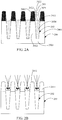
- FIG. 2A, FIG. 2B , FIG. 2C, and FIG. 2D show schematic diagrams (e.g., schematic cross-sectional views) that illustrate elements and/or structures formed in a method for manufacturing an memory device in accordance with one or more embodiments.
- the method may include steps S101, S102, S103, and S104.
- the step S101 may include preparing a substrate structure 200, a conductor 2011, and a conductor 2012.
- the substrate structure 200 may include a semiconductor substrate 2003, a semiconductor 2001, and a semiconductor 2002.
- the semiconductor 2001 and the semiconductor 2002 may be positioned on the semiconductor substrate 2003.
- the semiconductor 2002 may be spaced from the semiconductor 2001.
- the conductor 2011 may directly contact the semiconductor 2001.
- the conductor 2012 may be spaced from the first conducive member and may directly contact the semiconductor 2002.
- the first conductor 2011 and the second conductor 2012 may be formed of a conductive material, such as a polycrystalline silicon material, e.g., a doped polycrystalline silicon material.
- the substrate structure 200 and/or the semiconductor substrate 2003 may be/include at least one of a silicon substrate, a silicon-on-insulator (SOI) substrate, a strained-silicon-on-insulator (SSOI) substrate, a strained-silicon-germanium-on-insulator (S-SiGeOI), a silicon-germanium-on-insulator (SiGeOI) substrate, and a germanium-on-insulator (GeOI) substrate.
- SOI silicon-on-insulator
- SSOI strained-silicon-on-insulator
- SiGeOI silicon-germanium-on-insulator
- germanium-on-insulator (GeOI) substrate germanium-on-insulator
- the step S101 may include the following steps: preparing a substrate material layer (e.g., a semiconductor material layer); preparing a conductive material layer (e.g., a polycrystalline silicon material layer) on the substrate material layer; preparing a mask on the conductive material layer; partially removing (e.g., using an etching process) the conductive material layer and the substrate material layer to form the conductor 2011, the conductor 2012, the semiconductor 2001, the semiconductor 2002, and the semiconductor substrate 2003 and to form a trench 203 between the semiconductors 2001 and 2002 and between the conductors 2011 and 2012.
- a substrate material layer e.g., a semiconductor material layer
- preparing a conductive material layer e.g., a polycrystalline silicon material layer
- the step S102 may include preparing a dielectric material member 202 inside the trench 203.
- the dielectric material member 202 may be positioned between the semiconductor 2001 and the semiconductor 2002 and may directly contact each of the semiconductor 2001, the semiconductor 2002, the conductor 2011, and the conductor 2012.
- the dielectric member 202 may partially expose a sidewall of each of the conductors 2011 and 2012.
- the maximum height of the dielectric member 202 with reference to the bottom side of the substrate 2003 may be less than the maximum height of the conductor 2011 with reference to the bottom side of the substrate 2003.
- the maximum height of the dielectric member 202 with reference to the bottom side of the substrate 2003 may be greater than the maximum height of the semiconductor 2001 with reference to the bottom side of the substrate 2003.
- the dielectric material member 202 may include a dielectric portion 2021, a dielectric portion 2022, and a dielectric portion 2023.
- the dielectric portions 2021, 2022, and 2023 may be exposed.
- the dielectric portion 2021 may directly contact the conductor 2011 and may be connected through the dielectric portion 2022 to the dielectric portion 2023.
- the dielectric portion 2023 may directly contact the conductor 2012.
- the dielectric portions 2021 and 2023 may extend above the dielectric portion 2022 (given that the substrate 2003 is positioned below the dielectric portion 2022).
- the dielectric material member 202 may be formed of a dielectric material with a dielectric constant less than or equal to 3.9.
- the dielectric material member 202 may be formed of at least one of silicon oxide, silicon oxynitride, etc.
- the step S102 may include the following steps: providing a dielectric material layer that covers the mask and extends into the trench 203; planarizing (e.g., using a chemical-mechanical planarizing process) the dielectric material layer to remove a portion of the dielectric material layer that is positioned outside the trench 203, such that a dielectric material body may remain inside the trench 203 and may substantially or completely cover a sidewall of each of the conductors 2011 and 2012; removing (e.g., using a wet etching process) the mask; and partially removing (e.g., using a blank dry etching process) the dielectric material body to form the dielectric material member 202, which may partially expose sidewalls of the conductors 2011 and 2012.
- planarizing e.g., using a chemical-mechanical planarizing process
- the dielectric material layer to remove a portion of the dielectric material layer that is positioned outside the trench 203, such that a dielectric material body may remain inside the trench 203 and may substantially or completely cover
- the step S103 performing ion implantation on the dielectric material member 202 to form an implanted member 204 and a dielectric member 212.
- the step S103 may include providing at least one of arsenic ions, antimony ions, and bismuth ions to the dielectric material member 202 for forming the implanted member 204.
- a dose of the ion implantation (e.g., arsenic ion implantation) may be in a range of 1 x 10 ⁇ 10 ions/cm ⁇ 2 to 1 x 10 ⁇ 11 ions/cm ⁇ 2.
- the dielectric member 212 may be a portion of the dielectric material member 202 that is not substantially affected by the ion implantation.
- the implanted member 204 may directly contact each of the conductor 2011 and the conductor 2012.
- the implanted member 204 may include an implanted portion 2041, an implanted portion 2042, and an implanted portion 2043.
- the step S103 may include providing arsenic ions to the dielectric portions 2021, 2022, and 2023 of the dielectric material member 202 for forming the implanted portions 2041, 2042, and 2043 of the implanted member 204.
- the applied in the ion implantation may be sufficiently low, such that ions are implanted into the dielectric portions 2021, 2022, and 2023 without being implanted into a dielectric portion 2024 of the dielectric material member 202.
- the dielectric portion 2024 may be positioned closer to the semiconductor substrate 2003 than the dielectric portions 2021, 2022, and 2023, may not be exposed, and may not directly contact either of the conductors 2011 and 2012.
- the ions implanted into the dielectric portions 2021, 2022, and 2023 may weaken and/or destroy silicon-oxygen bonds in the dielectric portions 2021, 2022, and 2023 for forming the implanted portions 2041, 2042, and 2043.
- ions may be provided in a first direction, a second direction, and a third direction during the ion implantation.
- the first direction may be perpendicular to the bottom side of the semiconductor substrate 2003.
- Each of the second direction and the third direction may be at an acute angle with respect to the bottom side of the semiconductor substrate 2003.
- the minimum distance between the implanted member 204 and the bottom side of the semiconductor substrate 2003 may be greater than the minimum distance between the conductor 2011 and the bottom side of the semiconductor substrate 2003.
- the maximum height of the implanted member 204 with reference to the bottom side of the semiconductor substrate 2003 may be less than the maximum height of the conductor 2011 with reference to the bottom side of the semiconductor substrate 2003
- the dielectric member 212 may include a dielectric portion 2121 and a dielectric portion 2122.
- the implanted member 204 may be positioned between the dielectric portion 2121 and the dielectric portion 2122 in a direction parallel to the bottom side of the semiconductor substrate 2003.
- the implanted portion 2041 may be directly connected to the implanted portion 2042 and may be connected through the implanted portion 2042 to the implanted portion 2043.
- Each of the implanted portion 2041 and the implanted portion 2043 may extend above the implanted portion 2042 with the dielectric member 212 and/or the semiconductor substrate 2003 being positioned below the implanted portion 2042.
- the implanted portion 2041 may directly contact the conductor 2011.
- the implanted portion 2043 may directly contact the conductor 2012.
- a tangent of the implanted portion 2041 may be at an obtuse angle or a right angle with respect to a tangent of the implanted portion 2042 and/or with respect to the bottom side of the semiconductor substrate 2003.
- a tangent of the implanted portion 2043 may be at oblique or perpendicular with respect to the tangent of the implanted portion 2042 and/or with respect to the bottom side of the semiconductor substrate 2003.
- the dielectric portion 2121 may be positioned between the implanted portion 2041 and the conductor 2011 in the direction parallel to the bottom side of the semiconductor substrate 2003 and may directly contact each of the implanted portion 2041 and the conductor 2011.
- the dielectric portion 2122 may be positioned between the implanted portion 2043 and the conductor 2012 in the direction parallel to the bottom side of the semiconductor substrate 2003 and may directly contact each of the implanted portion 2042 and the conductor 2012.
- the dielectric portion 2121 may be positioned between the implanted portion 2041 and the conductor 2011 in a direction perpendicular to the bottom side of the semiconductor substrate 2003.
- the dielectric portion 2122 may be positioned between the implanted portion 2043 and the conductor 2012 in the direction perpendicular to the bottom side of the semiconductor substrate 2003.
- the dielectric portion 2121 may be positioned between the implanted portion 2041 and the semiconductor 2001 in the direction perpendicular to the bottom side of the semiconductor substrate 2003.
- the dielectric portion 2122 may be positioned between the implanted portion 2043 and the semiconductor 2002 in the direction perpendicular to the bottom side of the semiconductor substrate 2003.
- the step S104 may include removing the implanted member 204.
- the dielectric member 212 may be partially removed to form an isolation member 205.
- the step S104 may include performing an etching process (e.g., a wet etching process) to remove the implanted member 204.
- An etchant used in the etching process may be different from dilute hydrofluoric acid (DHF) and may not contain hydrofluoric acid (HF).
- the acidity of the etchant may be weaker than the acidity of the DHF.
- the etching process may also remove portions of the dielectric member 212, e.g., the dielectric portions 2121 and 2122, to form the isolation member 205, which may sufficiently insulate and/or isolate conductors 2011 and 2012 from each other.
- the method (e.g., the step S103) may include configuring one or more dimensions of the implanted member 204 (e.g., one or more thicknesses of one or more of the implanted portions 2041, 2042, and 2043) and/or configuring the etching process based on one or more target dimensions (e.g., a target thickness and/or a target height) of the isolation member 205 to be subsequently formed.
- the step S104 may include removing the implanted member 204 for exposing the isolation member 205.
- the method may include providing insulating layers (e.g., oxide-nitride-oxide layers) on the conductors 2011 and 2012.
- the method may include providing additional conductors on the insulating layers for implementing control gate electrodes of the memory device.
- an etch rate of the implanted member 204 corresponding to the etching process may be substantially higher than an etch rate of the material of the dielectric material member 202 (i.e., an etch rate of the material of the dielectric member 212) corresponding to the etching process.
- the etch rate of the implanted member 204 corresponding to the etching process may be higher than or equal to eight times the etch rate of the material of the dielectric material member 202 corresponding to the etching process.
- the unwanted dielectric portions 2021 and 2023 of the dielectric material member 202 may be effectively removed.
- the method may include configuring one or more dimensions of the implanted member 204 and/or configuring the etching process for implementing one or more dimension of the isolation member 205. Therefore, one or more suitable dimensions of the isolation member 205 may be attained.
Landscapes
- Semiconductor Memories (AREA)
- Non-Volatile Memory (AREA)
- Chemical & Material Sciences (AREA)
- Chemical Kinetics & Catalysis (AREA)
- General Chemical & Material Sciences (AREA)
- Element Separation (AREA)
Abstract
Description
- This application claims priority to and benefit of
Chinese Patent Application No. 201610006426.7, filed on 06 January 2016 - The technical field is related to a method for manufacturing a memory device, such as a flash memory device, e.g., a NAND memory device.
- A memory device may be used in write operations for storing data and may be used in read operations for retrieving data. A memory device may include floating gates and shallow trench isolation (STI) members positioned between the floating gates.
- In manufacturing of the memory device, after the STI members have been formed, some unwanted insulating material portions (e.g., oxide portions) may remain on sidewalls of the floating gates and may not be substantially removed. The remaining insulating material portions may negatively affect performance of the floating gates. As a result, performance and/or quality of the memory device may be unsatisfactory.
- A first aspect of the present invention relates to a method for manufacturing a memory device, such as a flash memory device, e.g., a NAND memory device.
- The method includes preparing a semiconductor substrate, a first semiconductor, a second semiconductor, a first conductor, and a second conductor. The first semiconductor and the second semiconductor are positioned on the semiconductor substrate. The second semiconductor is spaced from the first semiconductor. The first conductor directly contacts the first semiconductor. The second conductor is spaced from the first conducive member and directly contacts the second semiconductor. The first conductor and the second conductor function as floating gate electrodes of the memory device. The method further includes preparing a dielectric material member, which is positioned between the first semiconductor and the second semiconductor and directly contacts each of the first semiconductor, the second semiconductor, the first conductor, and the second conductor. The method further includes performing ion implantation on the dielectric material member to form an implanted member and a dielectric member. The method further includes removing the implanted member.
- The method may include performing an etching process (e.g., a wet etching process) to remove the implanted member. An etch rate of the implanted member corresponding to the etching process may be higher than an etch rate of a material of the dielectric material member corresponding to the etching process. The etch rate of the implanted member corresponding to the etching process is greater than or equal to eight times the etch rate of the material of the dielectric material member corresponding to the etching process. An etchant may be used in the etching process. The etchant may not include hydrofluoric acid.
- The method may include providing at least one of arsenic ions, antimony ions, and bismuth ions to the dielectric material member for forming the implanted member.
- The method preferably includes providing arsenic ions to the dielectric material member for forming the implanted member.
- Ions may be provided in a first direction and a second direction in the ion implantation. The first direction may be perpendicular to a bottom side of the semiconductor substrate. The second direction may be at an acute angle with respect to the bottom side of the semiconductor substrate.
- The method may include partially removing the dielectric member to form an isolation member in a process of removing the implanted member.
- The method may include configuring a dimension (e.g., thickness) of the implanted member based on a target dimension (e.g., target thickness) of the isolation member. The method may include removing the implanted member for exposing the isolation member.
- The implanted member may directly contact each of the first conductor and the second conductor.
- A minimum distance between the implanted member and the bottom side of the semiconductor substrate may be greater than a minimum distance between the first conductor and the bottom side of the semiconductor substrate.
- The implanted member maybe positioned between two portions of the dielectric member in a direction parallel to the bottom side of the semiconductor substrate.
- The implanted member may include a first implanted portion, a second implanted portion, and a third implanted portion. The first implanted portion may be directly connected to the second implanted portion and may be connected through the second implanted portion to the third implanted portion. Each of the first implanted portion and the third implanted portion may extend above the second implanted portion with reference to the dielectric member and/or with reference to the bottom side of the semiconductor substrate. The first implanted portion may directly contact the first conductor. The third implanted portion may directly contact the second conductor.
- A tangent of the first implanted portion may be at an obtuse angle with respect to a tangent of the second implanted portion and/or with respect to the bottom side of the semiconductor substrate.
- The dielectric member may include a first dielectric portion and a second dielectric portion. The first dielectric portion may be positioned between the first implanted portion and the first conductor in the direction parallel to the bottom side of the semiconductor substrate and may directly contact each of the first implanted portion and the first conductor. The second dielectric portion may be positioned between the third implanted portion and the second conductor in the direction parallel to the bottom side of the semiconductor substrate and may directly contact each of the third implanted portion and the second conductor.
- The first dielectric portion may be positioned between the first implanted portion and the first semiconductor in a direction perpendicular to the bottom side of the semiconductor substrate. The second dielectric portion may be positioned between the third implanted portion and the second semiconductor in the direction perpendicular to the bottom side of the semiconductor substrate.
- According to embodiments, in manufacturing of a memory device, unwanted insulating material portions (e.g., oxide portions) that have attached to sidewalls of floating gates (e.g., side walls of the first conductor and/or the second conductor) of the memory device may be effectively removed. As a result, satisfactory performance of the floating gates may be attained. Advantageously, satisfactory reliability and/or performance of the electromechanical device may be attained.
- The above summary is related to some of many embodiments of the invention disclosed herein and is not intended to limit the invention thereto.
-
-
FIG. 1 shows a flowchart that illustrates steps in a method for manufacturing a memory device in accordance with one or more embodiments. -
FIG. 2A, FIG. 2B ,FIG. 2C, and FIG. 2D show schematic diagrams (e.g., schematic cross-sectional views) that illustrate elements and/or structures formed in a method for manufacturing an memory device in accordance with one or more embodiments. - Example embodiments are described with reference to the accompanying drawings. Embodiments may be practiced without some or all of these specific details. Well known process steps and/or structures may not have been described in detail in order to not unnecessarily obscure described embodiments.
- The drawings and description are illustrative and not restrictive. Like reference numerals may designate like (e.g., analogous or identical) elements in the specification. Repetition of description may be avoided.
- The relative sizes and thicknesses of elements shown in the drawings are for facilitate description and understanding, without limiting possible embodiments. In the drawings, the thicknesses of some layers, films, panels, regions, etc., may be exaggerated for clarity.
- Illustrations of example embodiments in the figures may represent idealized illustrations. Variations from the shapes illustrated in the illustrations, as a result of, for example, manufacturing techniques and/or tolerances, may be possible. Thus, the example embodiments should not be construed as limited to the shapes or regions illustrated herein but are to include deviations in the shapes. For example, an etched region illustrated as a rectangle may have rounded or curved features. The shapes and regions illustrated in the figures are illustrative and should not limit the scope of the example embodiments.
- Although the terms "first", "second", etc. may be used herein to describe various elements, these elements should not be limited by these terms. These terms may be used to distinguish one element from another element. Thus, a first element discussed in this application may be termed a second element without departing from embodiments. The description of an element as a "first" element may not require or imply the presence of a second element or other elements. The terms "first", "second", etc. may also be used herein to differentiate different categories or sets of elements. For conciseness, the terms "first", "second", etc. may represent "first-category (or first-set)", "second-category (or second-set)", etc., respectively.
- If a first element (such as a layer, film, region, or substrate) is referred to as being "on", "neighboring", "connected to", or "coupled with" a second element, then the first element can be directly on, directly neighboring, directly connected to, or directly coupled with the second element, or an intervening element may also be present between the first element and the second element. If a first element is referred to as being "directly on", "directly neighboring", "directly connected to", or "directed coupled with" a second element, then no intended intervening element (except environmental elements such as air) may be provided between the first element and the second element.
- Spatially relative terms, such as "beneath", "below", "lower", "above", "upper", and the like, may be used herein for ease of description to describe one element or feature's spatial relationship to another element(s) or feature(s) as illustrated in the figures. It will be understood that the spatially relative terms may encompass different orientations of the device in use or operation in addition to the orientation depicted in the figures. For example, if the device in the figures is turned over, elements described as "below" or "beneath" other elements or features would then be oriented "above" the other elements or features. Thus, the term "below" can encompass both an orientation of above and below. The device may be otherwise oriented (rotated 90 degrees or at other orientations), and the spatially relative descriptors used herein should be interpreted accordingly.
- The terminology used herein is for the purpose of describing particular embodiments and is not intended to limit the embodiments. As used herein, the singular forms, "a", "an", and "the" may indicate plural forms as well, unless the context clearly indicates otherwise. The terms "includes" and/or "including", when used in this specification, may specify the presence of stated features, integers, steps, operations, elements, and/or components, but may not preclude the presence or addition of one or more other features, integers, steps, operations, elements, components, and/or groups.
- Unless otherwise defined, terms (including technical and scientific terms) used herein have the same meanings as commonly understood by one of ordinary skill in the art. Terms, such as those defined in commonly used dictionaries, should be interpreted as having meanings that are consistent with their meanings in the context of the relevant art and should not be interpreted in an idealized or overly formal sense unless expressly so defined herein.
- The term "connect" may mean "mechanically connect", "electrically connect", "directly connect", or "indirectly connect". The term "insulate" may mean "electrically insulate". The term "conductive" may mean "electrically conductive". The term "electrically connected" may mean "electrically connected without any intervening transistors". If a component (e.g., a transistor) is described as (electrically) connected between a first element and a second element, then a source/drain/input/output terminal of the component may be electrically connected to the first element through no intervening transistors, and a drain/source/output/input terminal of the component may be electrically connected to the second element through no intervening transistors.
- The term "conductor" may mean "electrically conductor". The term "insulator" may mean "electrically insulating member". The term "dielectric" may mean "dielectric member". The term "interconnect" may mean "interconnecting member". The term "prepare", the term "provide", or the term "form" may mean "prepare, provide, and/or form". The term "side" may mean "flat side", "planar side", or "straight side".
- Unless explicitly described to the contrary, the word "comprise" and variations such as "comprises", "comprising", "include", or "including" may imply the inclusion of stated elements but not the exclusion of other elements.
- Various embodiments, including methods and techniques, are described in this disclosure. Embodiments may also cover an article of manufacture that includes a non-transitory computer readable medium on which computer-readable instructions for carrying out embodiments of the inventive technique are stored. The computer readable medium may include, for example, semiconductor, magnetic, opto-magnetic, optical, or other forms of computer readable medium for storing computer readable code. Further, embodiments may also cover apparatuses for practicing embodiments. Such apparatus may include circuits, dedicated and/or programmable, to carry out operations pertaining to embodiments. Examples of such apparatus include a general purpose computer and/or a dedicated computing device when appropriately programmed and may include a combination of a computer/computing device and dedicated/programmable hardware circuits (such as electrical, mechanical, and/or optical circuits) adapted for the various operations pertaining to embodiments.
-
FIG. 1 shows a flowchart that illustrates steps in a method for manufacturing a memory device, such as a flash memory device, e.g., a NAND memory device, in accordance with one or more embodiments.FIG. 2A, FIG. 2B ,FIG. 2C, and FIG. 2D show schematic diagrams (e.g., schematic cross-sectional views) that illustrate elements and/or structures formed in a method for manufacturing an memory device in accordance with one or more embodiments. The method may include steps S101, S102, S103, and S104. - Referring to
FIG. 1 andFIG. 2A , the step S101 may include preparing asubstrate structure 200, aconductor 2011, and aconductor 2012. Thesubstrate structure 200 may include asemiconductor substrate 2003, asemiconductor 2001, and asemiconductor 2002. Thesemiconductor 2001 and thesemiconductor 2002 may be positioned on thesemiconductor substrate 2003. Thesemiconductor 2002 may be spaced from thesemiconductor 2001. Theconductor 2011 may directly contact thesemiconductor 2001. Theconductor 2012 may be spaced from the first conducive member and may directly contact thesemiconductor 2002. - The
first conductor 2011 and thesecond conductor 2012 may be formed of a conductive material, such as a polycrystalline silicon material, e.g., a doped polycrystalline silicon material. - The
substrate structure 200 and/or thesemiconductor substrate 2003 may be/include at least one of a silicon substrate, a silicon-on-insulator (SOI) substrate, a strained-silicon-on-insulator (SSOI) substrate, a strained-silicon-germanium-on-insulator (S-SiGeOI), a silicon-germanium-on-insulator (SiGeOI) substrate, and a germanium-on-insulator (GeOI) substrate. - The step S101 may include the following steps: preparing a substrate material layer (e.g., a semiconductor material layer); preparing a conductive material layer (e.g., a polycrystalline silicon material layer) on the substrate material layer; preparing a mask on the conductive material layer; partially removing (e.g., using an etching process) the conductive material layer and the substrate material layer to form the
conductor 2011, theconductor 2012, thesemiconductor 2001, thesemiconductor 2002, and thesemiconductor substrate 2003 and to form atrench 203 between thesemiconductors conductors - Referring to
FIG. 1 andFIG. 2A , the step S102 may include preparing adielectric material member 202 inside thetrench 203. Thedielectric material member 202 may be positioned between thesemiconductor 2001 and thesemiconductor 2002 and may directly contact each of thesemiconductor 2001, thesemiconductor 2002, theconductor 2011, and theconductor 2012. Thedielectric member 202 may partially expose a sidewall of each of theconductors dielectric member 202 with reference to the bottom side of thesubstrate 2003 may be less than the maximum height of theconductor 2011 with reference to the bottom side of thesubstrate 2003. The maximum height of thedielectric member 202 with reference to the bottom side of thesubstrate 2003 may be greater than the maximum height of thesemiconductor 2001 with reference to the bottom side of thesubstrate 2003. - The
dielectric material member 202 may include adielectric portion 2021, adielectric portion 2022, and adielectric portion 2023. Thedielectric portions dielectric portion 2021 may directly contact theconductor 2011 and may be connected through thedielectric portion 2022 to thedielectric portion 2023. Thedielectric portion 2023 may directly contact theconductor 2012. Thedielectric portions substrate 2003 is positioned below the dielectric portion 2022). - The
dielectric material member 202 may be formed of a dielectric material with a dielectric constant less than or equal to 3.9. Thedielectric material member 202 may be formed of at least one of silicon oxide, silicon oxynitride, etc. - The step S102 may include the following steps: providing a dielectric material layer that covers the mask and extends into the
trench 203; planarizing (e.g., using a chemical-mechanical planarizing process) the dielectric material layer to remove a portion of the dielectric material layer that is positioned outside thetrench 203, such that a dielectric material body may remain inside thetrench 203 and may substantially or completely cover a sidewall of each of theconductors dielectric material member 202, which may partially expose sidewalls of theconductors - Referring to
FIG. 1 ,FIG. 2A ,FIG. 2B , andFIG. 2C , the step S103 performing ion implantation on thedielectric material member 202 to form an implantedmember 204 and adielectric member 212. The step S103 may include providing at least one of arsenic ions, antimony ions, and bismuth ions to thedielectric material member 202 for forming the implantedmember 204. A dose of the ion implantation (e.g., arsenic ion implantation) may be in a range of 1 x 10^10 ions/cm^2 to 1 x 10^11 ions/cm^2. Thedielectric member 212 may be a portion of thedielectric material member 202 that is not substantially affected by the ion implantation. - The implanted
member 204 may directly contact each of theconductor 2011 and theconductor 2012. The implantedmember 204 may include an implantedportion 2041, an implantedportion 2042, and an implantedportion 2043. The step S103 may include providing arsenic ions to thedielectric portions dielectric material member 202 for forming the implantedportions member 204. The applied in the ion implantation may be sufficiently low, such that ions are implanted into thedielectric portions dielectric portion 2024 of thedielectric material member 202. Thedielectric portion 2024 may be positioned closer to thesemiconductor substrate 2003 than thedielectric portions conductors - The ions implanted into the
dielectric portions dielectric portions portions - Referring to
FIG. 2B , for effectively implanting ions into all thedielectric portions semiconductor substrate 2003. Each of the second direction and the third direction may be at an acute angle with respect to the bottom side of thesemiconductor substrate 2003. - Referring to
FIG. 2C , the minimum distance between the implantedmember 204 and the bottom side of thesemiconductor substrate 2003 may be greater than the minimum distance between theconductor 2011 and the bottom side of thesemiconductor substrate 2003. The maximum height of the implantedmember 204 with reference to the bottom side of thesemiconductor substrate 2003 may be less than the maximum height of theconductor 2011 with reference to the bottom side of thesemiconductor substrate 2003 - The
dielectric member 212 may include adielectric portion 2121 and adielectric portion 2122. The implantedmember 204 may be positioned between thedielectric portion 2121 and thedielectric portion 2122 in a direction parallel to the bottom side of thesemiconductor substrate 2003. - The implanted
portion 2041 may be directly connected to the implantedportion 2042 and may be connected through the implantedportion 2042 to the implantedportion 2043. Each of the implantedportion 2041 and the implantedportion 2043 may extend above the implantedportion 2042 with thedielectric member 212 and/or thesemiconductor substrate 2003 being positioned below the implantedportion 2042. The implantedportion 2041 may directly contact theconductor 2011. The implantedportion 2043 may directly contact theconductor 2012. A tangent of the implantedportion 2041 may be at an obtuse angle or a right angle with respect to a tangent of the implantedportion 2042 and/or with respect to the bottom side of thesemiconductor substrate 2003. A tangent of the implantedportion 2043 may be at oblique or perpendicular with respect to the tangent of the implantedportion 2042 and/or with respect to the bottom side of thesemiconductor substrate 2003. - The
dielectric portion 2121 may be positioned between the implantedportion 2041 and theconductor 2011 in the direction parallel to the bottom side of thesemiconductor substrate 2003 and may directly contact each of the implantedportion 2041 and theconductor 2011. Thedielectric portion 2122 may be positioned between the implantedportion 2043 and theconductor 2012 in the direction parallel to the bottom side of thesemiconductor substrate 2003 and may directly contact each of the implantedportion 2042 and theconductor 2012. - The
dielectric portion 2121 may be positioned between the implantedportion 2041 and theconductor 2011 in a direction perpendicular to the bottom side of thesemiconductor substrate 2003. Thedielectric portion 2122 may be positioned between the implantedportion 2043 and theconductor 2012 in the direction perpendicular to the bottom side of thesemiconductor substrate 2003. - The
dielectric portion 2121 may be positioned between the implantedportion 2041 and thesemiconductor 2001 in the direction perpendicular to the bottom side of thesemiconductor substrate 2003. Thedielectric portion 2122 may be positioned between the implantedportion 2043 and thesemiconductor 2002 in the direction perpendicular to the bottom side of thesemiconductor substrate 2003. - Referring to
FIG. 1 ,FIG. 2C, and FIG. 2D , the step S104 may include removing the implantedmember 204. In the step S104, thedielectric member 212 may be partially removed to form anisolation member 205. The step S104 may include performing an etching process (e.g., a wet etching process) to remove the implantedmember 204. An etchant used in the etching process may be different from dilute hydrofluoric acid (DHF) and may not contain hydrofluoric acid (HF). The acidity of the etchant may be weaker than the acidity of the DHF. [yI] - The etching process may also remove portions of the
dielectric member 212, e.g., thedielectric portions isolation member 205, which may sufficiently insulate and/or isolateconductors portions isolation member 205 to be subsequently formed. The step S104 may include removing the implantedmember 204 for exposing theisolation member 205. - The method may include providing insulating layers (e.g., oxide-nitride-oxide layers) on the
conductors - According to embodiments, an etch rate of the implanted
member 204 corresponding to the etching process may be substantially higher than an etch rate of the material of the dielectric material member 202 (i.e., an etch rate of the material of the dielectric member 212) corresponding to the etching process. In embodiments, the etch rate of the implantedmember 204 corresponding to the etching process may be higher than or equal to eight times the etch rate of the material of thedielectric material member 202 corresponding to the etching process. Therefore, by completely or partially turning thedielectric portions dielectric material member 202 into the implantedportions member 204, theunwanted dielectric portions 2021 and 2023 (and theunwanted dielectric portions 2121 and 2122), which have partially covered sidewalls of theconductors - In embodiments, the method may include configuring one or more dimensions of the implanted
member 204 and/or configuring the etching process for implementing one or more dimension of theisolation member 205. Therefore, one or more suitable dimensions of theisolation member 205 may be attained. - As a result, satisfactory performance of the
conductor isolation member 205 may be attained. Advantageously, satisfactory performance and/or quality of the memory device may be attained.
Claims (15)
- A method for manufacturing a memory device, the method comprising:preparing a first semiconductor, a second semiconductor, a first conductor, and a second conductor, wherein the second semiconductor is spaced from the first semiconductor, wherein the first conductor directly contacts the first semiconductor, and wherein the second conductor is spaced from the first conducive member and directly contacts the second semiconductor;preparing a dielectric material member, which is positioned between the first semiconductor and the second semiconductor and directly contacts each of the first semiconductor, the second semiconductor, the first conductor, and the second conductor;performing ion implantation on the dielectric material member to form an implanted member and a dielectric member; andremoving the implanted member.
- The method of claim 1, wherein removing the implanted member comprises:performing an etching process to remove the implanted member, wherein an etch rate of the implanted member corresponding to the etching process is higher than an etch rate of a material of the dielectric material member corresponding to the etching process;wherein preferably the etch rate of the implanted member corresponding to the etching process is greater than or equal to eight times the etch rate of the material of the dielectric material member corresponding to the etching process.
- The method of claim 1 or 2, wherein removing the implanted member comprises:using an etchant to remove the implanted member, wherein the etchant is free of hydrofluoric acid.
- The method of any one of the claims 1-3 comprising:providing at least one of arsenic ions, antimony ions, and bismuth ions to the dielectric material member for forming the implanted member; and/orproviding arsenic ions to the dielectric material member for forming the implanted member.
- The method of any one of the claims 1-4,
wherein the first semiconductor and the second semiconductor are positioned on a semiconductor substrate,
wherein ions are provided in a first direction and a second direction in the ion implantation,
wherein the first direction is perpendicular to a bottom side of the semiconductor substrate, and
wherein the second direction is at an acute angle with respect to the bottom side of the semiconductor substrate. - The method of any one of the claims 1-5, wherein a process for removing the implanted member comprises: partially removing the dielectric member to form an isolation member;
wherein preferably a dimension of the implanted member is configured based on a target dimension of the isolation member, and the implanted member is removed for exposing the isolation member. - The method of any one of the claims 1-6, wherein the implanted member directly contacts each of the first conductor and the second conductor.
- The method of any one of the claims 1-7, wherein the first semiconductor and the second semiconductor are positioned on a semiconductor substrate, and
wherein a minimum distance between the implanted member and a bottom side of the semiconductor substrate is greater than a minimum distance between the first conductor and the bottom side of the semiconductor substrate; and/or
wherein the implanted member is positioned between two portions of the dielectric member in a direction parallel to a bottom side of the semiconductor substrate. - The method of any one of the claims 1-8,
wherein the implanted member comprises a first implanted portion and a second implanted portion directly connected to each other, and
wherein a tangent of the first implanted portion is at an obtuse angle or a right angle with respect to a tangent of the second implanted portion. - The method of claim 9, wherein the dielectric member comprises a first dielectric portion, wherein the first dielectric portion is positioned between the first implanted portion and the first conductor and directly contacts each of the first implanted portion and the first conductor.
- The method of claim 10,
wherein the first semiconductor and the second conducting member are positioned on a semiconductor substrate, and
wherein the first dielectric portion is positioned between the first implanted portion and the first conductor in a direction parallel to a bottom side of the semiconductor substrate;
wherein preferably the first dielectric portion is positioned between the first implanted portion and the first semiconductor in a direction perpendicular to the bottom side of the semiconductor substrate. - The method of claim 8,
wherein the implanted member comprises a third implanted portion, wherein the first implanted portion is connected through the second implanted portion to the third implanted portion, and
wherein each of the first implanted portion and the third implanted portion extends above the second implanted portion. - The method of claim 8,
wherein the implanted member comprises a third implanted portion,
wherein a tangent of the third implanted portion is oblique or perpendicular with respect to the tangent of the second implanted portion,
wherein the first implanted portion is connected through the second implanted portion to the third implanted portion,
wherein the first implanted portion directly contacts the first conductor, and
wherein the third implanted portion directly contacts the second conductor. - The method of claim 13,
wherein the first semiconductor and the second semiconductor are positioned on a semiconductor substrate,
wherein the dielectric member comprises a first dielectric portion and a second dielectric portion,
wherein the first dielectric portion is positioned between the first implanted portion and the first conductor in a direction parallel to a bottom side of the semiconductor substrate and directly contacts each of the first implanted portion and the first conductor, and
wherein the second dielectric portion is positioned between the third implanted portion and the second conductor in the direction parallel to the bottom side of the semiconductor substrate and directly contacts each of the third implanted portion and the second conductor. - The method of claim 14,
wherein the first dielectric portion is positioned between the first implanted portion and the first semiconductor in a direction perpendicular to the bottom side of the semiconductor substrate, and
wherein the second dielectric portion is positioned between the third implanted portion and the second semiconductor in the direction perpendicular to the bottom side of the semiconductor substrate.
Applications Claiming Priority (1)
| Application Number | Priority Date | Filing Date | Title |
|---|---|---|---|
| CN201610006426.7A CN106952922B (en) | 2016-01-06 | 2016-01-06 | A method of manufacturing a semiconductor device |
Publications (1)
| Publication Number | Publication Date |
|---|---|
| EP3190609A1 true EP3190609A1 (en) | 2017-07-12 |
Family
ID=57714465
Family Applications (1)
| Application Number | Title | Priority Date | Filing Date |
|---|---|---|---|
| EP16207185.6A Withdrawn EP3190609A1 (en) | 2016-01-06 | 2016-12-28 | Method for manufacturing memory device |
Country Status (3)
| Country | Link |
|---|---|
| US (1) | US10002783B2 (en) |
| EP (1) | EP3190609A1 (en) |
| CN (1) | CN106952922B (en) |
Families Citing this family (7)
| Publication number | Priority date | Publication date | Assignee | Title |
|---|---|---|---|---|
| CN108109656B (en) * | 2017-12-28 | 2020-10-27 | 上海华力微电子有限公司 | Flash memory array fabrication method and flash memory array |
| TWI661540B (en) * | 2018-04-16 | 2019-06-01 | Winbond Electronics Corp. | Method of manufacturing memory device |
| CN110416218B (en) * | 2018-04-27 | 2021-05-04 | 华邦电子股份有限公司 | Manufacturing method of memory element |
| CN110649025B (en) * | 2018-06-26 | 2023-08-08 | 华邦电子股份有限公司 | Method for forming memory device |
| CN110491877B (en) * | 2019-08-23 | 2022-10-25 | 上海华虹宏力半导体制造有限公司 | Flash memory manufacturing method |
| CN113471207A (en) * | 2020-03-30 | 2021-10-01 | 中芯国际集成电路制造(上海)有限公司 | Semiconductor structure and forming method thereof |
| CN113906550B (en) * | 2021-08-31 | 2026-04-10 | 长江存储科技有限责任公司 | A semiconductor device and its fabrication method |
Citations (3)
| Publication number | Priority date | Publication date | Assignee | Title |
|---|---|---|---|---|
| US20120032267A1 (en) * | 2010-08-06 | 2012-02-09 | International Business Machines Corporation | Device and method for uniform sti recess |
| US20130137251A1 (en) * | 2011-11-30 | 2013-05-30 | Taiwan Semiconductor Manufacturing Company, Ltd. | Uniform Shallow Trench Isolation Regions and the Method of Forming the Same |
| US20150187634A1 (en) * | 2013-12-27 | 2015-07-02 | Taiwan Semiconductor Manufacturing Co., Ltd | Mechanisms for forming finfets with different fin heights |
Family Cites Families (6)
| Publication number | Priority date | Publication date | Assignee | Title |
|---|---|---|---|---|
| US4652334A (en) * | 1986-03-06 | 1987-03-24 | General Motors Corporation | Method for patterning silicon dioxide with high resolution in three dimensions |
| US5874346A (en) * | 1996-05-23 | 1999-02-23 | Advanced Micro Devices, Inc. | Subtrench conductor formation with large tilt angle implant |
| TW406356B (en) * | 1998-08-24 | 2000-09-21 | United Microelectronics Corp | A method of manufacturing shallow trench isolation structure |
| KR100406180B1 (en) * | 2001-12-22 | 2003-11-17 | 주식회사 하이닉스반도체 | Method of manufacturing a flash memory cell |
| US7541240B2 (en) * | 2005-10-18 | 2009-06-02 | Sandisk Corporation | Integration process flow for flash devices with low gap fill aspect ratio |
| CN105097681A (en) * | 2014-05-06 | 2015-11-25 | 中芯国际集成电路制造(上海)有限公司 | Semiconductor device, preparation method thereof, and electronic device |
-
2016
- 2016-01-06 CN CN201610006426.7A patent/CN106952922B/en active Active
- 2016-11-16 US US15/352,823 patent/US10002783B2/en active Active
- 2016-12-28 EP EP16207185.6A patent/EP3190609A1/en not_active Withdrawn
Patent Citations (3)
| Publication number | Priority date | Publication date | Assignee | Title |
|---|---|---|---|---|
| US20120032267A1 (en) * | 2010-08-06 | 2012-02-09 | International Business Machines Corporation | Device and method for uniform sti recess |
| US20130137251A1 (en) * | 2011-11-30 | 2013-05-30 | Taiwan Semiconductor Manufacturing Company, Ltd. | Uniform Shallow Trench Isolation Regions and the Method of Forming the Same |
| US20150187634A1 (en) * | 2013-12-27 | 2015-07-02 | Taiwan Semiconductor Manufacturing Co., Ltd | Mechanisms for forming finfets with different fin heights |
Also Published As
| Publication number | Publication date |
|---|---|
| US10002783B2 (en) | 2018-06-19 |
| CN106952922A (en) | 2017-07-14 |
| US20170194189A1 (en) | 2017-07-06 |
| CN106952922B (en) | 2020-04-14 |
Similar Documents
| Publication | Publication Date | Title |
|---|---|---|
| US10002783B2 (en) | Method for manufacturing memory device | |
| KR102732926B1 (en) | Step structure of 3D memory device and its formation method | |
| US11532726B2 (en) | VDMOS device and manufacturing method therefor | |
| KR100881818B1 (en) | Method of forming a semiconductor device | |
| US9825133B2 (en) | Semiconductor device and related manufacturing method | |
| US9590059B2 (en) | Interdigitated capacitor to integrate with flash memory | |
| CN113013255B (en) | Split gate memory and manufacturing method thereof | |
| EP3193372A1 (en) | Semiconductor device and related manufacturing method | |
| US9773778B2 (en) | Semiconductor device, related manufacturing method, and related electronic device | |
| US9520483B2 (en) | Method for manufacturing semiconductor device | |
| CN103915439A (en) | Semiconductor device and manufacturing method thereof | |
| CN113906550B (en) | A semiconductor device and its fabrication method | |
| CN111200011B (en) | Semiconductor device and method of forming the same | |
| US9978760B2 (en) | Semiconductor device and related manufacturing method | |
| KR100317488B1 (en) | Method of manufacturing a flash memory device | |
| US20150340375A1 (en) | Semiconductor device, related manufacturing method, and related electronic device | |
| KR100937818B1 (en) | Flash memory device and manufacturing method thereof | |
| CN109638016B (en) | Flash memory and forming method thereof | |
| US20070087538A1 (en) | Method of manufacturing nand flash memory device | |
| EP3163619A1 (en) | Semiconductor device and related manufacturing method | |
| US20180144992A1 (en) | Method of fabrication of a fet transistor having an overlapped gate | |
| CN223528413U (en) | Semiconductor structure and memory | |
| US20070158735A1 (en) | Method of fabricating a transistor | |
| US7517755B2 (en) | Method for fabricating semiconductor device | |
| US8536019B2 (en) | Semiconductor devices having encapsulated isolation regions and related fabrication methods |
Legal Events
| Date | Code | Title | Description |
|---|---|---|---|
| PUAI | Public reference made under article 153(3) epc to a published international application that has entered the european phase |
Free format text: ORIGINAL CODE: 0009012 |
|
| STAA | Information on the status of an ep patent application or granted ep patent |
Free format text: STATUS: THE APPLICATION HAS BEEN PUBLISHED |
|
| AK | Designated contracting states |
Kind code of ref document: A1 Designated state(s): AL AT BE BG CH CY CZ DE DK EE ES FI FR GB GR HR HU IE IS IT LI LT LU LV MC MK MT NL NO PL PT RO RS SE SI SK SM TR |
|
| AX | Request for extension of the european patent |
Extension state: BA ME |
|
| RAP1 | Party data changed (applicant data changed or rights of an application transferred) |
Owner name: SEMICONDUCTOR MANUFACTURING INTERNATIONAL CORPORAT |
|
| STAA | Information on the status of an ep patent application or granted ep patent |
Free format text: STATUS: REQUEST FOR EXAMINATION WAS MADE |
|
| 17P | Request for examination filed |
Effective date: 20171218 |
|
| RBV | Designated contracting states (corrected) |
Designated state(s): AL AT BE BG CH CY CZ DE DK EE ES FI FR GB GR HR HU IE IS IT LI LT LU LV MC MK MT NL NO PL PT RO RS SE SI SK SM TR |
|
| RAP1 | Party data changed (applicant data changed or rights of an application transferred) |
Owner name: SEMICONDUCTOR MANUFACTURING INTERNATIONAL (BEIJING Owner name: SEMICONDUCTOR MANUFACTURING INTERNATIONAL (SHANGHA |
|
| STAA | Information on the status of an ep patent application or granted ep patent |
Free format text: STATUS: EXAMINATION IS IN PROGRESS |
|
| 17Q | First examination report despatched |
Effective date: 20181113 |
|
| STAA | Information on the status of an ep patent application or granted ep patent |
Free format text: STATUS: THE APPLICATION IS DEEMED TO BE WITHDRAWN |
|
| 18D | Application deemed to be withdrawn |
Effective date: 20210903 |