EP3190588A1 - Mr sensor and card reader - Google Patents
Mr sensor and card reader Download PDFInfo
- Publication number
- EP3190588A1 EP3190588A1 EP15838810.8A EP15838810A EP3190588A1 EP 3190588 A1 EP3190588 A1 EP 3190588A1 EP 15838810 A EP15838810 A EP 15838810A EP 3190588 A1 EP3190588 A1 EP 3190588A1
- Authority
- EP
- European Patent Office
- Prior art keywords
- resistor
- track
- card
- sensor
- recorded
- Prior art date
- Legal status (The legal status is an assumption and is not a legal conclusion. Google has not performed a legal analysis and makes no representation as to the accuracy of the status listed.)
- Granted
Links
Images





Classifications
-
- G—PHYSICS
- G06—COMPUTING OR CALCULATING; COUNTING
- G06K—GRAPHICAL DATA READING; PRESENTATION OF DATA; RECORD CARRIERS; HANDLING RECORD CARRIERS
- G06K7/00—Methods or arrangements for sensing record carriers, e.g. for reading patterns
- G06K7/08—Methods or arrangements for sensing record carriers, e.g. for reading patterns by means detecting the change of an electrostatic or magnetic field, e.g. by detecting change of capacitance between electrodes
- G06K7/082—Methods or arrangements for sensing record carriers, e.g. for reading patterns by means detecting the change of an electrostatic or magnetic field, e.g. by detecting change of capacitance between electrodes using inductive or magnetic sensors
- G06K7/083—Methods or arrangements for sensing record carriers, e.g. for reading patterns by means detecting the change of an electrostatic or magnetic field, e.g. by detecting change of capacitance between electrodes using inductive or magnetic sensors inductive
- G06K7/084—Methods or arrangements for sensing record carriers, e.g. for reading patterns by means detecting the change of an electrostatic or magnetic field, e.g. by detecting change of capacitance between electrodes using inductive or magnetic sensors inductive sensing magnetic material by relative movement detecting flux changes without altering its magnetised state
-
- G—PHYSICS
- G01—MEASURING; TESTING
- G01R—MEASURING ELECTRIC VARIABLES; MEASURING MAGNETIC VARIABLES
- G01R33/00—Arrangements or instruments for measuring magnetic variables
- G01R33/02—Measuring direction or magnitude of magnetic fields or magnetic flux
- G01R33/06—Measuring direction or magnitude of magnetic fields or magnetic flux using galvano-magnetic devices
- G01R33/09—Magnetoresistive devices
-
- G—PHYSICS
- G06—COMPUTING OR CALCULATING; COUNTING
- G06K—GRAPHICAL DATA READING; PRESENTATION OF DATA; RECORD CARRIERS; HANDLING RECORD CARRIERS
- G06K7/00—Methods or arrangements for sensing record carriers, e.g. for reading patterns
- G06K7/08—Methods or arrangements for sensing record carriers, e.g. for reading patterns by means detecting the change of an electrostatic or magnetic field, e.g. by detecting change of capacitance between electrodes
-
- G—PHYSICS
- G06—COMPUTING OR CALCULATING; COUNTING
- G06Q—INFORMATION AND COMMUNICATION TECHNOLOGY [ICT] SPECIALLY ADAPTED FOR ADMINISTRATIVE, COMMERCIAL, FINANCIAL, MANAGERIAL OR SUPERVISORY PURPOSES; SYSTEMS OR METHODS SPECIALLY ADAPTED FOR ADMINISTRATIVE, COMMERCIAL, FINANCIAL, MANAGERIAL OR SUPERVISORY PURPOSES, NOT OTHERWISE PROVIDED FOR
- G06Q20/00—Payment architectures, schemes or protocols
- G06Q20/30—Payment architectures, schemes or protocols characterised by the use of specific devices or networks
- G06Q20/34—Payment architectures, schemes or protocols characterised by the use of specific devices or networks using cards, e.g. integrated circuit [IC] cards or magnetic cards
- G06Q20/341—Active cards, i.e. cards including their own processing means, e.g. including an IC or chip
-
- G—PHYSICS
- G07—CHECKING-DEVICES
- G07F—COIN-FREED OR LIKE APPARATUS
- G07F19/00—Complete banking systems; Coded card-freed arrangements adapted for dispensing or receiving monies or the like and posting such transactions to existing accounts, e.g. automatic teller machines
- G07F19/20—Automatic teller machines [ATMs]
- G07F19/205—Housing aspects of ATMs
- G07F19/2055—Anti-skimming aspects at ATMs
-
- G—PHYSICS
- G07—CHECKING-DEVICES
- G07F—COIN-FREED OR LIKE APPARATUS
- G07F7/00—Mechanisms actuated by objects other than coins to free or to actuate vending, hiring, coin or paper currency dispensing or refunding apparatus
- G07F7/08—Mechanisms actuated by objects other than coins to free or to actuate vending, hiring, coin or paper currency dispensing or refunding apparatus by coded identity card or credit card or other personal identification means
- G07F7/086—Mechanisms actuated by objects other than coins to free or to actuate vending, hiring, coin or paper currency dispensing or refunding apparatus by coded identity card or credit card or other personal identification means by passive credit-cards adapted therefor, e.g. constructive particularities to avoid counterfeiting, e.g. by inclusion of a physical or chemical security-layer
-
- G—PHYSICS
- G11—INFORMATION STORAGE
- G11B—INFORMATION STORAGE BASED ON RELATIVE MOVEMENT BETWEEN RECORD CARRIER AND TRANSDUCER
- G11B25/00—Apparatus characterised by the shape of record carrier employed but not specific to the method of recording or reproducing, e.g. dictating apparatus; Combinations of such apparatus
- G11B25/04—Apparatus characterised by the shape of record carrier employed but not specific to the method of recording or reproducing, e.g. dictating apparatus; Combinations of such apparatus using flat record carriers, e.g. disc, card
-
- G—PHYSICS
- G11—INFORMATION STORAGE
- G11B—INFORMATION STORAGE BASED ON RELATIVE MOVEMENT BETWEEN RECORD CARRIER AND TRANSDUCER
- G11B5/00—Recording by magnetisation or demagnetisation of a record carrier; Reproducing by magnetic means; Record carriers therefor
- G11B5/127—Structure or manufacture of heads, e.g. inductive
- G11B5/33—Structure or manufacture of flux-sensitive heads, i.e. for reproduction only; Combination of such heads with means for recording or erasing only
- G11B5/39—Structure or manufacture of flux-sensitive heads, i.e. for reproduction only; Combination of such heads with means for recording or erasing only using magneto-resistive devices or effects
-
- G—PHYSICS
- G06—COMPUTING OR CALCULATING; COUNTING
- G06K—GRAPHICAL DATA READING; PRESENTATION OF DATA; RECORD CARRIERS; HANDLING RECORD CARRIERS
- G06K19/00—Record carriers for use with machines and with at least a part designed to carry digital markings
- G06K19/06—Record carriers for use with machines and with at least a part designed to carry digital markings characterised by the kind of the digital marking, e.g. shape, nature, code
- G06K19/08—Record carriers for use with machines and with at least a part designed to carry digital markings characterised by the kind of the digital marking, e.g. shape, nature, code using markings of different kinds or more than one marking of the same kind in the same record carrier, e.g. one marking being sensed by optical and the other by magnetic means
- G06K19/10—Record carriers for use with machines and with at least a part designed to carry digital markings characterised by the kind of the digital marking, e.g. shape, nature, code using markings of different kinds or more than one marking of the same kind in the same record carrier, e.g. one marking being sensed by optical and the other by magnetic means at least one kind of marking being used for authentication, e.g. of credit or identity cards
-
- G—PHYSICS
- G07—CHECKING-DEVICES
- G07F—COIN-FREED OR LIKE APPARATUS
- G07F7/00—Mechanisms actuated by objects other than coins to free or to actuate vending, hiring, coin or paper currency dispensing or refunding apparatus
- G07F7/08—Mechanisms actuated by objects other than coins to free or to actuate vending, hiring, coin or paper currency dispensing or refunding apparatus by coded identity card or credit card or other personal identification means
- G07F7/0806—Details of the card
- G07F7/0813—Specific details related to card security
- G07F7/082—Features insuring the integrity of the data on or in the card
-
- G—PHYSICS
- G07—CHECKING-DEVICES
- G07F—COIN-FREED OR LIKE APPARATUS
- G07F7/00—Mechanisms actuated by objects other than coins to free or to actuate vending, hiring, coin or paper currency dispensing or refunding apparatus
- G07F7/08—Mechanisms actuated by objects other than coins to free or to actuate vending, hiring, coin or paper currency dispensing or refunding apparatus by coded identity card or credit card or other personal identification means
- G07F7/10—Mechanisms actuated by objects other than coins to free or to actuate vending, hiring, coin or paper currency dispensing or refunding apparatus by coded identity card or credit card or other personal identification means together with a coded signal, e.g. in the form of personal identification information, like personal identification number [PIN] or biometric data
- G07F7/1008—Active credit-cards provided with means to personalise their use, e.g. with PIN-introduction/comparison system
Definitions
- the present invention relates to an MR sensor for a card reader which is used in a card reader structured to read magnetic data recorded in a card. Further, the present invention relates to a card reader comprising the MR sensor.
- Patent Literature 1 a card reader which is structured to read magnetic data recorded in a card (see, for example, Patent Literature 1).
- the card reader described in Patent Literature 1 includes a magnetic head for reading magnetic data recorded in a card. Further, the card reader includes a pre-head (magnetic head) for detecting whether or not magnetic data are recorded in a magnetic stripe of a card which has been inserted into a card insertion port.
- an objective of the present invention is to provide an MR sensor for a card reader which is capable of preventing illegal acquisition of magnetic information by a criminal and reducing its cost although the MR sensor is capable of detecting whether magnetic data are recorded in a magnetic stripe of a card or not when it is mounted on a card reader. Further, an objective of the present invention is to provide a card reader comprising the MR sensor.
- the present invention provides an MR sensor for a card reader structured to detect whether or not magnetic data are recorded in a magnetic stripe of a card, which is provided with the magnetic stripe in which magnetic data are capable of being recorded in a first track and magnetic data are capable of being recorded in a second track.
- the MR sensor includes a first resistor and a second resistor which are serially-connected with each other and are disposed at positions where the first track is passed, and a third resistor and a fourth resistor which are serially-connected with each other and are disposed at positions where the second track is passed.
- the second resistor and the fourth resistor are connected with a power supply, the first resistor and the third resistor are grounded, and a potential difference between a first midpoint between the first resistor and the second resistor serially-connected with each other and a second midpoint between the third resistor and the fourth resistor serially-connected with each other is an output of the MR sensor.
- the MR sensor in accordance with the present invention is structured as described above and thus, in a case that the MR sensor is mounted on a card reader, when a card in which magnetic data are recorded in a magnetic stripe is passed through a disposed position of the MR sensor, a signal different from a signal corresponding to magnetic data recorded in the card is capable of being outputted from the MR sensor. Therefore, according to the present invention, when the MR sensor is mounted on a card reader, illegal acquisition of magnetic information by a criminal is capable of being prevented although the MR sensor is capable of detecting whether magnetic data are recorded in a magnetic stripe of a card or not.
- a signal different from a signal corresponding to magnetic data recorded in a card is capable being outputted from the MR sensor by devising arrangement and the like of the first through the fourth resistors. Therefore, a structure of the MR sensor can be simplified and, as a result, a cost of the MR sensor can be reduced.
- the first resistor and the second resistor are disposed in a separated state from each other in a passing direction of the card by a distance of odd number times of a half of a bit interval of the first track when "0" data are recorded in the first track
- the third resistor and the fourth resistor are disposed in a separated state from each other in the passing direction of the card by a distance of odd number times of a half of a bit interval of the second track when "0" data are recorded in the second track.
- each of the first resistor, the second resistor, the third resistor and the fourth resistor is formed by being folded back a plurality of times in a direction perpendicular to a passing direction of the card. According to this structure, an electric current flowing through the first through the fourth resistors can be made small. Therefore, electric power consumption of the MR sensor can be restrained.
- the present invention provides an MR sensor for a card reader structured to detect whether or not magnetic data are recorded in a magnetic stripe of a card, which is provided with the magnetic stripe in which magnetic data are capable of being recorded in a first track and magnetic data are capable of being recorded in a second track.
- the MR sensor includes a first resistor and a second resistor which are serially-connected with each other, and a third resistor and a fourth resistor which are serially-connected with each other.
- the first resistor and the fourth resistor are disposed at positions where the first track is passed, the second resistor and the third resistor are disposed at positions where the second track is passed, the second resistor and the fourth resistor are connected with a power supply, and the first resistor and the third resistor are grounded.
- Each of the first resistor, the second resistor, the third resistor and the fourth resistor is formed by being folded back two times or more in a first direction perpendicular to a passing direction of the card, and a potential difference between a first midpoint between the first resistor and the second resistor serially-connected with each other and a second midpoint between the third resistor and the fourth resistor serially-connected with each other is an output of the MR sensor.
- the MR sensor in accordance with the present invention is structured as described above and thus, in a case that the MR sensor is mounted on a card reader, when a card in which magnetic data are recorded in a magnetic stripe is passed through a disposed position of the MR sensor, a signal different from a signal corresponding to magnetic data recorded in the card can be outputted from the MR sensor. Therefore, according to the present invention, when the MR sensor is mounted on a card reader, illegal acquisition of magnetic information by a criminal is capable being prevented although the MR sensor is capable of detecting whether magnetic data are recorded in a magnetic stripe of a card or not.
- a signal different from a signal corresponding to magnetic data recorded in a card can be outputted from the MR sensor by devising arrangement, shapes and the like of the first through the fourth resistors. Therefore, a structure of the MR sensor can be simplified and, as a result, a cost of the MR sensor can be reduced.
- an interval of two times of a bit interval of the first track when "0" data are recorded in the first track is defined as " ⁇ 1 "
- an interval of two times of a bit interval of the second track when "0" data are recorded in the second track is defined as " ⁇ 2 "
- "n 1 " and “n 2 " are an integer of 0 or more
- "m” is an integer of 3 or more
- each of the first resistor, the second resistor, the third resistor and the fourth resistor is formed by being folded back "m-1" times in the first direction
- the first resistor comprises "m” pieces of a first resistance part which are formed in a straight line shape parallel to the first direction and are disposed at a pitch of (n 1 ⁇ 1 / m + ⁇ 1 / 2m) in a passing direction of the card
- the second resistor comprises "m” pieces of a second resistance part which are formed in a straight line shape parallel to the first direction and are disposed at a pitch of (n
- respective amplitudes of resistance change rates of the first resistor, the second resistor, the third resistor and the fourth resistor can be made small when a card in which magnetic data are recorded in a magnetic stripe is passed through a disposed position of the MR sensor.
- the present invention provides an MR sensor for a card reader structured to detect whether or not magnetic data are recorded in a magnetic stripe of a card, which is provided with the magnetic stripe in which magnetic data are capable of being recorded in a first track and magnetic data are capable of being recorded in a second track.
- the MR sensor includes a first resistor and a second resistor which are serially-connected with each other, and a third resistor and a fourth resistor which are serially-connected with each other.
- the first resistor is disposed at a position where the first track is passed
- the fourth resistor is disposed at a position where the second track is passed
- the second resistor and the fourth resistor are connected with a power supply
- the first resistor and the third resistor are grounded.
- Each of the first resistor and the fourth resistor is formed by being folded back two times or more in a first direction perpendicular to a passing direction of the card
- each of the second resistor and the third resistor is formed in a straight line shape parallel to the first direction.
- the first resistor includes three or more pieces of a first resistance part which is formed in a straight line shape parallel to the first direction
- the fourth resistor includes three or more pieces of a fourth resistance part which is formed in a straight line shape parallel to the first direction.
- a width of the second resistor in a passing direction of the card is set to be 1/10 or less of a width of the first resistance part in the passing direction of the card
- a width of the third resistor in the passing direction of the card is set to be 1/10 or less of a width of the fourth resistance part in the passing direction of the card
- a potential difference between a first midpoint between the first resistor and the second resistor serially-connected with each other and a second midpoint between the third resistor and the fourth resistor serially-connected with each other is an output of the MR sensor.
- the present invention provides an MR sensor for a card reader structured to detect whether or not magnetic data are recorded in a magnetic stripe of a card, which is provided with the magnetic stripe in which magnetic data are capable of being recorded in a first track and magnetic data are capable of being recorded in a second track.
- the MR sensor includes a first resistor and a second resistor which are serially-connected with each other, a third resistor and a fourth resistor which are serially-connected with each other, the first resistor is disposed at a position where the first track is passed, the fourth resistor is disposed at a position where the second track is passed, the second resistor and the fourth resistor are connected with a power supply, and the first resistor and the third resistor are grounded.
- Each of the first resistor and the fourth resistor is formed by being folded back two times or more in a first direction perpendicular to a passing direction of the card, each of the second resistor and the third resistor is formed by being folded back once or more in the passing direction of the card, and a potential difference between a first midpoint between the first resistor and the second resistor serially-connected with each other and a second midpoint between the third resistor and the fourth resistor serially-connected with each other is an output of the MR sensor.
- the second resistor is disposed at a position where the first track is passed
- the third resistor is disposed at a position where the second track is passed.
- the present invention provides an MR sensor for a card reader structured to detect whether or not magnetic data are recorded in a magnetic stripe of a card, which is provided with the magnetic stripe in which magnetic data are capable of being recorded in a first track and magnetic data are capable of being recorded in a second track.
- the MR sensor includes a first resistor and a second resistor which are serially-connected with each other, a third resistor and a fourth resistor which are serially-connected with each other, the first resistor is disposed at a position where the first track is passed, and the fourth resistor is disposed at a position where the second track is passed.
- the second resistor and the third resistor are disposed at positions displaced from the position where the first track is passed and at positions displaced from the position where the second track is passed, and the second resistor and the fourth resistor are connected with a power supply, and the first resistor and the third resistor are grounded.
- Each of the first resistor and the fourth resistor is formed by being folded back two times or more in a first direction perpendicular to a passing direction of the card, and a potential difference between a first midpoint between the first resistor and the second resistor serially-connected with each other and a second midpoint between the third resistor and the fourth resistor serially-connected with each other is an output of the MR sensor.
- the MR sensor in accordance with the present invention is structured as described above and thus, in a case that the MR sensor is mounted on a card reader, when a card in which magnetic data are recorded in a magnetic stripe is passed through a disposed position of the MR sensor, a signal different from a signal corresponding to magnetic data recorded in the card is capable of being outputted from the MR sensor. Therefore, according to the present invention, when the MR sensor is mounted on a card reader, illegal acquisition of magnetic information by a criminal can be prevented although the MR sensor is capable of detecting whether magnetic data are recorded in a magnetic stripe of a card or not.
- a signal different from a signal corresponding to magnetic data recorded in a card can be outputted from the MR sensor by devising arrangement, shapes and the like of the first through the fourth resistors. Therefore, a structure of the MR sensor can be simplified and, as a result, a cost of the MR sensor can be reduced.
- each of the first resistor and the fourth resistor is formed by being folded back "m-1" times in the first direction
- the first resistor includes "m” pieces of a first resistance part which are formed in a straight line shape parallel to the first direction and are disposed at a pitch of (n 1 ⁇ 1 / m + ⁇ 1 / 2m) in a passing direction of the card
- the fourth resistor includes "m” pieces of a fourth resistance part which are formed in a straight line shape parallel to the first direction and are disposed at a pitch of (n 2 ⁇ 2 / m +
- the MR sensor in accordance with the present invention may be used in a card reader including a card insertion part which is formed with a card insertion port into which the card is inserted and in which the MR sensor is disposed.
- a card reader illegal acquisition of magnetic information by a criminal can be prevented although the MR sensor is capable of detecting whether magnetic data are recorded in a magnetic stripe of a card or not.
- a cost of the MR sensor can be reduced and, as a result, a cost of the card reader can be reduced.
- the MR sensor when the MR sensor is mounted on a card reader, illegal acquisition of magnetic information by a criminal can be prevented although the MR sensor is capable of detecting whether or not magnetic data are recorded in a magnetic stripe of a card, and a cost of the MR sensor can be reduced.
- FIG. 1 is a schematic view showing a card reader 1 in accordance with an embodiment of the present invention.
- FIG. 2 is a view showing a rear face of a card 2 shown in FIG. 1 .
- a card reader 1 in this embodiment is a device which is structured to perform reading of magnetic data recorded on a card 2 and/or recording of magnetic data on a card 2, and is, for example, mounted and used in a predetermined host apparatus such as an ATM.
- the card reader 1 includes a card insertion part 4 formed with an insertion port 3 into which a card 2 is inserted, and a main body part 5.
- a card passage 6 where a card 2 inserted into the insertion port 3 is passed is formed in an inside of the card reader 1.
- a card 2 is passed in the "X” direction shown in Fig. 1 .
- the "X” direction is a passing direction of a card 2.
- the "Z" direction in Fig. 1 perpendicular to the "X” direction is a thickness direction of a card 2 which is taken into the card reader 1
- the "Y” direction in Fig. 1 perpendicular to the "X” direction and the “Z” direction is a width direction of a card 2 taken into the card reader 1.
- a card 2 is, for example, a rectangular card made of vinyl chloride whose thickness is about 0.7-0.8mm.
- a magnetic stripe 2a in which magnetic data are recorded is formed on a rear face of the card 2.
- the magnetic stripe 2a is formed along a longitudinal direction of a card 2 which is formed in a substantially rectangular shape.
- a card 2 is inserted into the card reader 1 in a state that its rear face faces a lower side and, in a state that a longitudinal direction of a card 2 is substantially coincided with the "X" direction (passing direction of a card 2), and is conveyed in an inside of the card reader 1.
- an IC chip and/or an antenna for communication may be incorporated in the card 2.
- the card 2 may be a PET (polyethylene terephthalate) card whose thickness is about 0.18-0.36mm or may be a paper card having a predetermined thickness.
- Three tracks of magnetic data comprised of a track 2b, a track 2c and a track 2d are recordable in the magnetic stripe 2a.
- the track 2b, the track 2c and the track 2d are arranged in this order in a short-side direction of a card 2.
- magnetic data of the track 2c and/or magnetic data of the track 2d are recorded in the magnetic stripe 2a.
- Recording density of magnetic data of the track 2c is 75bpi (bit per inch) and recording density of magnetic data of the track 2d is 210bpi.
- the track 2c in this embodiment is a first track and the track 2d is a second track.
- recording density of magnetic data of the track 2b is 210bpi.
- the card reader 1 includes a magnetic head 7 structured to perform reading of magnetic data recorded in a magnetic stripe 2a of a card 2 and/or recording magnetic data to the magnetic stripe 2a, drive rollers 8 and pad rollers 9 structured to convey the card 2 along a card passage 6, and an MR sensor 10 structured to detect whether magnetic data are recorded in the magnetic stripe 2a of the card 2 or not.
- the magnetic head 7, the drive rollers 8 and the pad rollers 9 are arranged in the main body part 5.
- the magnetic head 7 includes three channels so as to be capable of individually reading magnetic data of the three tracks 2b through 2d.
- the MR sensor 10 is disposed in the card insertion part 4. Next, a specific structure of the MR sensor 10 will be described below.
- FIG. 3 is a circuit diagram showing an MR sensor 10 in FIG. 1 .
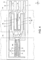
- FIG. 4 is a plan view showing an MR sensor 10 in accordance with a first embodiment of the present invention.
- FIGs. 5(A) and 5(B) are views for explaining a difference between an output signal of a magnetic head 7 shown in FIG. 1 and an output signal of an MR sensor 10 shown in FIG. 4 .
- FIG. 5(A) is a view showing one example of an output signal of a magnetic head 7
- FIG. 5(B) is a view showing one example of an output signal of an MR sensor 10.
- the MR sensor 10 is, as shown in FIG. 3 , provided with a first resistor "R1" (hereinafter, referred to as a resistor “R1”) and a second resistor “R2" (hereinafter, referred to as a resistor “R2”) which are serially-connected with each other, and a third resistor “R3” (hereinafter, referred to as a resistor “R3”) and a fourth resistor “R4" (hereinafter, referred to as a resistor "R4") which are serially-connected with each other.
- the resistors “R1” through “R4" are, for example, formed of a thin film of ferronickel alloy.
- the resistor "R1" and the resistor “R2” are connected in parallel with the resistor “R3” and the resistor "R4".
- the resistors “R1” through “R4" may be formed of material other than ferronickel alloy.
- the resistor "R2" and the resistor "R4" are connected with a power supply "Vcc". Specifically, one end of the resistor “R2" which is not connected with the resistor “R1” and one end of the resistor “R4" which is not connected with the resistor “R3” are connected with a connection terminal "T1" for the power supply "Vcc” and the connection terminal "T1" is connected with the power supply "Vcc”. The resistor "R1" and the resistor "R3" are grounded.
- one end of the resistor "R1" which is not connected with the resistor "R2” and one end of the resistor "R3” which is not connected with the resistor “R4" are connected with a ground terminal "T2" and the ground terminal "T2" is grounded.
- the resistors "R1" through “R4" are formed by being folded back a plurality of times in the "Y” direction (short-side direction of a card 2). In this embodiment, the resistors “R1” through “R4" are formed by being folded back two times in the "Y” direction.
- the resistor “R1” is provided with three pieces of a first resistance part 11 which is formed in a straight line shape parallel to the "Y” direction.
- the resistor “R2” is provided with three pieces of a second resistance part 12 which is formed in a straight line shape parallel to the "Y” direction.
- the resistor “R3” is provided with three pieces of a third resistance part 13 which is formed in a straight line shape parallel to the "Y” direction.
- the resistor “R4" is provided with three pieces of a fourth resistance part 14 which is formed in a straight line shape parallel to the "Y” direction.
- the resistor "R1" and the resistor “R2” are disposed at the same position in the "Y” direction. Specifically, the resistor “R1” and the resistor “R2” are disposed at a position where the track 2c is passed in the "Y” direction. Further, the resistor “R1” and the resistor “R2” are disposed in a separated state from each other by a distance “D1” in the "X” direction.
- the distance “D1” is set to be a distance of odd number times of a half of a bit interval of the track 2c when "0" data are recorded in the track 2c.
- a pitch “P1" in the "X” direction of three pieces of the first resistance part 11 is set to be an integral multiple of a bit interval of the track 2c when "0" data are recorded in the track 2c.
- the pitch “P1” is set to be the bit interval in the track 2c when "0" data are recorded in the track 2c and the pitch “P1” is 0.34mm.
- a pitch “P2" in the "X" direction of three pieces of the second resistance part 12 is set to be equal to the pitch "P1".
- resistor "R1" and the resistor “R2” are formed line-symmetrically with respect to an imaginary line “IL1” parallel to the "Y” direction which passes a center position in the "X” direction between the resistor "R1” and the resistor “R2” when viewed in the "Z” direction.
- the resistor "R3" and the resistor “R4" are disposed at the same position in the "Y” direction. Specifically, the resistor “R3” and the resistor “R4" are disposed at a position in the "Y” direction where the track 2d is passed. Further, the resistor “R3” and the resistor “R4" are disposed in a separated state from each other by a distance “D2" in the "X” direction.
- the distance “D2" is set to be a distance of odd number times of a half of a bit interval of the track 2d when "0" data are recorded in the track 2d.
- a pitch “P3" in the "X” direction of three pieces of the third resistance part 13 is set to be an integral multiple of a bit interval of the track 2d when "0" data are recorded in the track 2d.
- the pitch “P3” is set to be the bit interval of the track 2d when "0" data are recorded in the track 2d and the pitch "P3" is 0.12mm.
- a pitch "P4" in the "X" direction of three pieces of the fourth resistance part 12 is set to be equal to the pitch "P3".
- the resistor "R3" and the resistor “R4" are formed line-symmetrically with respect to an imaginary line “IL2" parallel to the "Y” direction which passes a center position in the "X” direction between the resistor "R3” and the resistor “R4" when viewed in the "Z” direction.
- the imaginary line “IL1” and the imaginary line “IL2” are disposed on the same straight line.
- a length in the "Y” direction of the first resistance part 11, a length in the "Y” direction of the second resistance part 12, a length in the “Y” direction of the third resistance part 13, and a length in the "Y” direction of the fourth resistance part 14 are set to be equal to each other. Further, the length is set to be narrower than a width of the track 2c and a width of the track 2d in the "Y” direction. For example, the length is 2mm. Further, a width in the "X" direction of the first resistance part 11, a width in the "X” direction of the second resistance part 12, a width in the "X” direction of the third resistance part 13, and a width in the "X” direction of the fourth resistance part 14 are set to be equal to each other.
- the width is 80 ⁇ m.
- a film thickness of the resistor "R1", a film thickness of the resistor “R2”, a film thickness of the resistor “R3”, and a film thickness of the resistor "R4" are set to be equal to each other.
- the film thickness is 45nm.
- a potential difference (in other words, voltage) between a first midpoint “C1" between the resistor “R1” and the resistor “R2” serially-connected with each other (the connecting point of the resistor “R1” with the resistor “R2”) and a second midpoint “C2” between the resistor “R3” and the resistor “R4" serially-connected with each other (the connecting point of the resistor “R3” with the resistor “R4") is an output of the MR sensor 10.
- a card 2 in which magnetic data are recorded in a magnetic stripe 2a (more specifically, a card 2 in which magnetic data in a track 2c and/or magnetic data in a track 2d are recorded) is passed through a disposed position of the MR sensor 10, a signal is outputted from the MR sensor 10.
- the output signal "SG3" of the MR sensor 10 is different from a signal corresponding to magnetic data recorded in the magnetic stripe 2a (in other words, different from the output signals "SG1" and "SG2" of the magnetic head 7).
- a magnetic field generated by magnetic data in the track 2c is stronger than a magnetic field generated by magnetic data in the track 2d. Therefore, as shown in FIG. 5(A) , an amplitude of the output signal "SG2" is smaller than an amplitude of the output signal "SG1". Further, as shown in FIG. 5(B) , an amplitude of the midpoint potential "V2" is smaller than an amplitude of the midpoint potential "V1".
- the output signal "SG3" of the MR sensor 10 is different from a signal corresponding to magnetic data recorded in the magnetic stripe 2a (different from the output signals "SG1" and "SG2" of the magnetic head 7). Therefore, according to this embodiment, even when the MR sensor 10 is capable of detecting whether magnetic data are recorded in the magnetic stripe 2a or not, illegal acquisition of magnetic information by a criminal can be prevented.
- the output signal "SG3" of the MR sensor 10 can be made different from a signal corresponding to the magnetic data recorded in a magnetic stripe 2a by devising shapes and/or arrangement of the resistors "R1" through “R4". Therefore, a structure of the MR sensor 10 can be simplified and, as a result, a cost of the MR sensor 10 can be reduced.
- the resistor "R1" and the resistor “R2” are disposed in a separated state from each other by a distance “D1" in the "X” direction.
- the distance “D1” is set to be a distance of odd number times of a half of a bit interval of the track 2c when "0" data are recorded in the track 2c.
- the resistor "R3" and the resistor “R4" are disposed in a separated state from each other by a distance "D2" in the "X” direction.
- the distance “D2” is set to be a distance of odd number times of a half of a bit interval of the track 2d when "0" data are recorded in the track 2d.
- an amplitude of the output signal "SG3" outputted from the MR sensor 10 can be increased. Accordingly, in this embodiment, it can be further appropriately detected whether magnetic data are recorded in a magnetic stripe 2a of a card 2 or not.
- the resistors "R1" through “R4" are formed so as to be folded back a plurality of times in the "Y" direction. Therefore, according to this embodiment, an electric current flowing through the resistors "R1” through “R4" can be reduced. Accordingly, in this embodiment, electric power consumption of the MR sensor 10 can be restrained.
- the resistors "R1" through “R4" are formed by being folded back a plurality of times in the "Y” direction.
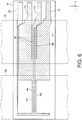
- the resistors “R1” through “R4" may be formed in a straight line shape parallel to the "Y” direction as shown in FIG. 6 .
- the resistor "R1” and the resistor “R2” are disposed in a separated state from each other by a distance "D1" in the "X” direction
- the resistor "R3" and the resistor "R4" are disposed in a separated state from each other by a distance "D2" in the "X” direction.
- the resistor "R1" and the resistor “R2” are disposed at substantially the same position as each other and the resistor "R3" and the resistor “R4" are disposed at substantially the same position as each other.
- the same reference signs are used in the same structures as the embodiment described above.
- the distance “D1" between the resistor “R1” and the resistor “R2” is set to be a distance of odd number times of a half of a bit interval of a track 2c when "0" data are recorded in the track 2c.
- the distance “D1” may be a distance other than a distance of odd number times of a half of a bit interval of a track 2c when "0" data are recorded in the track 2c.
- the distance “D2" between the resistor “R3” and the resistor “R4" is set to be a distance of odd number times of a half of a bit interval of a track 2d when "0" data are recorded in the track 2d.
- the distance “D2” may be a distance other than a distance of odd number times of a half of a bit interval of a track 2d when "0" data are recorded in the track 2d.
- the pitch "P1" of the first resistance parts 11 and the pitch “P2" of the second resistance parts 12 are set to be an integral multiple of a bit interval of the track 2c when "0" data are recorded in the track 2c.
- the pitches “P1” and “P2” may be values other than an integral multiple of a bit interval of the track 2c when "0" data are recorded in the track 2c.
- the pitch “P3" of the third resistance parts 13 and the pitch “P4" of the fourth resistance parts 14 are set to be an integral multiple of a bit interval of the track 2d when "0" data are recorded in the track 2d.
- the pitches “P3” and “P4" may be values other than an integral multiple of a bit interval of the track 2d when "0” data are recorded in the track 2d.
- FIG. 7 is a plan view showing an MR sensor 10 in accordance with a second embodiment of the present invention.
- FIG. 8 is a view showing an example of an output signal of an MR sensor 10 shown in FIG. 7 .
- a structure of an MR sensor 10 in a second embodiment is different from the MR sensor 10 in the first embodiment. Therefore, in the following descriptions, a structure of an MR sensor 10 in accordance with a second embodiment will be described below mainly on differences between the structure of the MR sensor 10 in the first embodiment and a structure of an MR sensor 10 in the second embodiment.
- FIG. 7 the same reference signs are used in the same structures as the first embodiment.
- an MR sensor 10 in this embodiment includes a resistor "R1” and a resistor “R2” serially-connected with each other and a resistor “R3” and a resistor “R4" serially-connected with each other.
- the resistor “R1” and the resistor “R2” are connected in parallel with the resistor “R3” and the resistor “R4".
- the resistor “R2” and the resistor “R4" are connected with a power supply "Vcc" and the resistor "R1” and the resistor “R3” are grounded.
- a circuit diagram of the MR sensor 10 in this embodiment is the same as the circuit diagram shown in FIG. 3 .
- the resistors "R1" through “R4" are formed by being folded back “m-1” times in the “Y” direction.
- the resistors “R1” through “R4" are formed by being folded back two times or more in the "Y” direction.
- "m” 4
- the resistors "R1” through “R4" are formed by being folded back three times in the "Y” direction.
- the resistor "R1” is provided with four pieces ("m" pieces) of a first resistance part 11 which is formed in a straight line shape parallel to the "Y" direction.
- the resistor "R2" is provided with four pieces ("m” pieces) of a second resistance part 12 which is formed in a straight line shape parallel to the "Y” direction.
- the resistor “R3” is provided with four pieces ("m” pieces) of a third resistance part 13 which is formed in a straight line shape parallel to the "Y” direction.
- the resistor “R4" is provided with four pieces ("m” pieces) of a fourth resistance part 14 which is formed in a straight line shape parallel to the "Y” direction.
- the "Y” direction in this embodiment is a first direction.
- the resistor "R1" and the resistor “R4" are disposed at the same position in the "Y” direction. Specifically, the resistor “R1” and the resistor “R4" are disposed at a position where the track 2c is passed in the "Y” direction. Further, the resistor “R1” and the resistor “R4" are disposed in a separated state from each other by a predetermined distance (for example, 1.06mm) in the "X" direction.
- the resistor “R2” and the resistor “R3” are disposed at the same position in the "Y” direction. Specifically, the resistor “R2” and the resistor “R3” are disposed at a position in the "Y” direction where the track 2d is passed.
- the resistor "R2" and the resistor “R3” are disposed in a separated state from each other by a predetermined distance (for example, 1.09mm) in the "X" direction. Further, in the "X” direction, the resistor “R1” and the resistor “R2” are disposed at substantially the same position as each other and the resistor "R3” and the resistor “R4" are disposed at substantially the same position as each other.
- an interval of two times of a bit interval of the track 2c when "0" data are recorded in the track 2c are defined as " ⁇ 1 "
- an interval of two times of a bit interval of the track 2d when "0" data are recorded in the track 2d are defined as " ⁇ 2 "
- n 1 " and “n 2 " are an integer of 0 or more and, as described above, "m” is an integer of 3 or more.
- a pitch "P1" of four pieces of the first resistance part 11 in the "X” direction and a pitch “P4" of four pieces of the fourth resistance part 14 in the "X” direction are set to be (n 1 ⁇ 1 / m + ⁇ 1 / 2m), and a pitch “P2" of four pieces of the second resistance part 12 in the "X” direction and a pitch “P3” of four pieces of the third resistance part 13 in the "X” direction are set to be (n 2 ⁇ 2 / m + ⁇ 2 / 2m).
- a length of the first resistance part 11 in the "Y” direction, a length of the second resistance part 12 in the “Y” direction, a length of the third resistance part 13 in the “Y” direction, and a length of the fourth resistance part 14 in the “Y” direction are set to be equal to each other.
- the length is 2mm.
- a width of the first resistance part 11 in the "X” direction, a width of the second resistance part 12 in the “X” direction, a width of the third resistance part 13 in the "X” direction, and a width of the fourth resistance part 14 in the "X” direction are set to be equal to each other.
- the width is 80 ⁇ m.
- a film thickness of the resistor "R1", a film thickness of the resistor “R2”, a film thickness of the resistor “R3”, and a film thickness of the resistor “R4" are set to be equal to each other.
- the film thickness is 45nm.
- a potential difference between a first midpoint "C1" between the resistor “R1” and the resistor “R2” serially-connected with each other and a second midpoint “C2" between the resistor “R3” and the resistor “R4" serially-connected with each other is an output of the MR sensor 10. Therefore, when a card 2 in which magnetic data in a track 2c and/or magnetic data in a track 2d are recorded is passed through a disposed position of the MR sensor 10, a signal is outputted from the MR sensor 10.
- the output signal "SG3" of the MR sensor 10 is different from a signal corresponding to magnetic data recorded in the magnetic stripe 2a (in other words, different from the output signals "SG1" and "SG2" of the magnetic head 7).
- the pitch "P1" of the first resistance part 11 in the "X” direction and the pitch “P4" of the fourth resistance part 14 in the “X” direction are set to be (n 1 ⁇ 1 / m + ⁇ 1 / 2m), and the pitch “P2" of the second resistance part 12 in the “X” direction and the pitch “P3” of the third resistance part 13 in the "X” direction are set to be (n 2 ⁇ 2 m + ⁇ 2 / 2m).
- the output signal "SG3" from the MR sensor 10 is varied at a period which is different from a period of the signal corresponding to magnetic data recorded in the magnetic stripe 2a but is varied in a shape close to the signal corresponding to the magnetic data recorded in the magnetic stripe 2a. Therefore, in the first embodiment, in a case that magnetic data are recorded in only one of the track 2c or the track 2d, magnetic information may be illegally acquired by a criminal.
- the output signal "SG3" of the MR sensor 10 becomes a signal completely different from the signal corresponding to magnetic data recorded in the magnetic stripe 2a. Therefore, according to this embodiment, even when magnetic data are recorded in only one of the track 2c or the track 2d, illegal acquisition of magnetic information by a criminal can be prevented.
- the pitch "P1" of the first resistance part 11 and the pitch “P4" of the fourth resistance part 14 are set to be (n 1 ⁇ 1 / m + ⁇ 1 / 2m).
- the pitches “P1” and “P4" may be set to be a value other than the value of (n 1 ⁇ 1 / m + ⁇ 1 / 2m).
- the pitch "P2" of four pieces of the second resistance part 12 and the pitch “P3" of four pieces of the third resistance part 13 are set to be (n 2 ⁇ 2 / m + ⁇ 2 / 2m).
- the pitches “P2" and “P3” may be a value other than the value of (n 2 ⁇ 2 / m + ⁇ 2 / 2m). Further, in the embodiment described above, the pitch “P1” and the pitch “P4" are equal to each other, but the pitch “P1” and the pitch “P4" may be different from each other. Similarly, in the embodiment described above, the pitch “P2” and the pitch “P3” are equal to each other, but the pitch “P2” and the pitch “P3” may be different from each other.
- FIG. 9 is a plan view showing an MR sensor 10 in accordance with a third embodiment of the present invention.
- FIG. 10(A) is a graph showing a relationship between resistance change rates " ⁇ 1" and “ ⁇ 2" of a first through a fourth resistors “R1" through “R4" shown in FIG. 9 and magnetic flux density.
- FIG. 10(A) is a graph showing a relationship between resistance change rates " ⁇ 1" and “ ⁇ 2" of a first through a fourth resistors "R1" through “R4" shown in FIG. 9 and magnetic flux density.
- FIG. 10(B) is a table showing a resistance change rate " ⁇ 1" of resistors “R2” and “R3", a resistance change rate “ ⁇ 2” of resistors “R1” and “R4" and a ratio between a resistance change rate " ⁇ 1” of resistors “R2” and “R3” and a resistance change rate “ ⁇ 2” of resistors “R1” and “R4" when magnetic flux density is a predetermined value in FIG. 10(A) .
- FIG. 11 is a view showing an example of an output signal of an MR sensor shown in FIG. 9 .
- a structure of an MR sensor 10 in a third embodiment is different from the MR sensors 10 in the first and the second embodiments. Therefore, in the following descriptions, a structure of an MR sensor 10 in accordance with a third embodiment will be described below mainly on differences between the structures of the MR sensors 10 in the first and the second embodiments and a structure of an MR sensor 10 in the third embodiment.
- the same reference signs are used in the same structures as the first and the second embodiments.
- an MR sensor 10 in this embodiment includes a resistor "R1” and a resistor “R2” serially-connected with each other and a resistor “R3” and a resistor “R4" serially-connected with each other.
- the resistor “R1” and the resistor “R2” are connected in parallel with the resistor “R3” and the resistor “R4".
- the resistor “R2” and the resistor “R4" are connected with a power supply "Vcc" and the resistor "R1” and the resistor “R3” are grounded.
- a circuit diagram of the MR sensor 10 in this embodiment is the same as the circuit diagram shown in FIG. 3 .
- the resistors "R1" and “R4" are formed by being folded back “m-1" times in the "Y” direction.
- the resistors “R1” and “R4" are formed by being folded back two times or more in the "Y” direction.
- “m” 4
- the resistors "R1” and “R4" are formed by being folded back three times in the "Y” direction.
- the resistor "R1” is provided with four pieces ("m" pieces) of a first resistance part 11 which is formed in a straight line shape parallel to the "Y" direction.
- the resistor "R4" is provided with four pieces ("m” pieces) of a fourth resistance part 14 which is formed in a straight line shape parallel to the "Y" direction.
- the resistor "R2" and the resistor “R3” are formed in a straight line shape parallel to the "Y" direction.
- the resistor "R1" and the resistor “R2” are disposed so that a center of the resistor “R1” in the “Y” direction and a center of the resistor “R2” in the “Y” direction are substantially coincided with each other. Further, the resistor “R1” and the resistor “R2” are disposed at a position in the "Y” direction where the track 2c is passed. Further, the resistor “R1” and the resistor “R2” are disposed in a separated state from each other by a predetermined distance in the "X" direction.
- the resistor "R3" and the resistor “R4" are disposed so that a center of the resistor “R3” in the “Y” direction and a center of the resistor “R4" in the “Y” direction are substantially coincided with each other. Further, the resistor “R3” and the resistor “R4" are disposed at a position in the "Y” direction where the track 2d is passed. Further, the resistor “R3” and the resistor “R4" are disposed in a separated state from each other by a predetermined distance in the "X” direction. The resistor “R1” and the resistor “R4" are disposed substantially at the same position as each other in the "X” direction.
- an interval of two times of a bit interval of the track 2c when "0" data are recorded in the track 2c are defined as " ⁇ 1 "
- an interval of two times of a bit interval of the track 2d when "0" data are recorded in the track 2d are defined as “ ⁇ 2 "
- "n 1 " and "n 2 " are an integer of 0 or more and, as described above, "m” is an integer of 3 or more.
- a pitch "P1" of four pieces of the first resistance part 11 in the "X" direction is set to be (n 1 ⁇ 1 / m + ⁇ 1 / 2m).
- a pitch "P4" of four pieces of the fourth resistance part 14 in the "X” direction is set to be (n 2 ⁇ 2 / m + ⁇ 2 / 2m).
- " ⁇ 1 " is 0.68mm
- "X 2 " is 0.24mm
- a width of the resistor "R2" in the “X” direction is set to be 1/10 or less of a width of the first resistance part 11 in the “X” direction. Further, a width of the resistor “R3" in the “X” direction is set to be 1/10 or less of a width of the fourth resistance part 14 in the "X” direction. In this embodiment, a width of the first resistance part 11 and a width of the fourth resistance part 14 in the "X” direction are, for example, 80 ⁇ m, and a width of the resistor "R2" and a width of the resistor “R3” in the "X” direction are, for example, 5 ⁇ m.
- a length of the first resistance part 11 in the "Y” direction and a length of the fourth resistance part 14 in the “Y” direction are equal to each other and, for example, the length is 2mm.
- a length of the resistor "R2" in the “Y” direction and a length of the resistor “R3” in the “Y” direction are equal to each other and, for example, the length is 0.5mm.
- a film thickness of the resistor "R1", a film thickness of the resistor “R2”, a film thickness of the resistor "R3”, and a film thickness of the resistor "R4" are equal to each other and, for example, the film thickness is 45nm.
- a width of the resistor "R2" and a width of the resistor “R3” in the “X” direction are 5 ⁇ m and thus the widths of the resistors “R2” and “R3” in the “X” direction are narrow. Therefore, even when magnetic fields are applied to the resistors “R2” and “R3” (in other words, even when a card 2 in which magnetic data are recorded in a track 2c and a track 2d is passed through disposed positions of the resistor "R2" and “R3”), resistance change rates of the resistors “R2" and “R3” are extremely small.
- the width of the resistors "R2" and “R3" in the "X” direction is set to be 1/10 of the width of the first resistance part 11 and the fourth resistance part 14 in the "X” direction
- the resistance change rate " ⁇ 1" of the resistors “R2” and “R3” with respect to strength of a magnetic field is varied as shown by the broken line in FIG. 10(A)
- the resistance change rate " ⁇ 2" of the resistors "R1” and “R4" with respect to a magnetic flux density is varied as shown by the solid line in FIG. 10(A) .
- a magnetic flux density of magnetic data recorded in a magnetic stripe 2a of a card 2 is commonly from 0.5mT (milli-Tesla) to 3mT.
- widths of the resistor "R2" and “R3” in the “X” direction are set to be 1/10 of the widths in the “X” direction of the first resistance part 11 and the fourth resistance part 14, a ratio of the resistance change rate " ⁇ 1" with respect to the resistance change rate “ ⁇ 2” can be suppressed in 1/3 or less.
- widths of the resistors "R2" and “R3” in the "X” direction are set to be further smaller than 1/10 of the widths in the "X” direction of the first resistance part 11 and the fourth resistance part 14, a ratio of the resistance change rate " ⁇ 1" with respect to the resistance change rate " ⁇ 2" can be made further small.
- a potential difference between a first midpoint "C1" between the resistor “R1” and the resistor “R2” serially-connected with each other and a second midpoint “C2" between the resistor “R3” and the resistor “R4" serially-connected with each other is an output of the MR sensor 10. Therefore, when a card 2 in which magnetic data in a track 2c and/or magnetic data in a track 2d are recorded is passed through a disposed position of the MR sensor 10, a signal is outputted from the MR sensor 10.
- the output signal "SG3" of the MR sensor 10 is different from a signal corresponding to magnetic data recorded in the magnetic stripe 2a (in other words, different from the output signals "SG1" and "SG2" of the magnetic head 7).
- a ratio of the resistance change rate " ⁇ 1" with respect to the resistance change rate " ⁇ 2" can be suppressed to 1/3 or less and thus a large amplitude of the output signal "SG3" of the MR sensor 10 can be secured.
- the pitch "P1" in the "X” direction of the first resistance part 11 is set to be (n 1 ⁇ 1 / m + ⁇ 1 / 2m), and the pitch "P4" in the "X” direction of the fourth resistance part 14 is set to be (n 2 ⁇ 2 / m + ⁇ 2 / 2m). Therefore, an amplitude of each of resistance change rates of the resistor "R1" and the resistor "R4" when a card 2 in which magnetic data are recorded in a magnetic stripe 2a is passed through a disposed position of the MR sensor 10 can be made small.
- the output signal "SG3" of the MR sensor 10 becomes a signal completely different from the signal corresponding to magnetic data recorded in the magnetic stripe 2a. Therefore, according to this embodiment, even when magnetic data are recorded in only one of the track 2c or the track 2d, illegal acquisition of magnetic information by a criminal can be prevented.
- an output of the MR sensor 10 may be lowered at a predetermined timing when a card 2 in which magnetic data are recorded in a magnetic stripe 2a is passed through a disposed position of the MR sensor 10 and accuracy of detection of the MR sensor 10 is deteriorated.
- occurrence of this problem can be prevented.
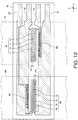
- FIG. 12 is a plan view showing an MR sensor 10 in accordance with a modified embodiment of the third embodiment of the present invention.
- FIG. 13 is a plan view showing an MR sensor 10 in accordance with a modified embodiment of the third embodiment of the present invention.
- the resistor "R2" and the resistor “R3” are formed in a straight line shape parallel to the "Y” direction.
- the present invention is not limited to this embodiment.
- the resistor “R2" and the resistor “R3” may be formed by being folded back a plurality of times in the "X” direction.
- the resistor “R2” and the resistor “R3” may be formed by being folded back a plurality of times in the "X” direction so that portions of the resistors "R2" and “R3" parallel to the "X” direction become longer than portions of the resistors "R2" and “R3” parallel to the "Y” direction.
- the resistor “R2” and/or the resistor “R3” may be formed by being folded back once in the "X” direction.
- resistance change rates of the resistors "R2" and “R3” when magnetic fields are applied to the resistors "R2" and “R3” are extremely small. Therefore, also in this case, an output signal "SG3" of the MR sensor 10 when a card 2 in which magnetic data are recorded in a magnetic stripe 2a is passed through a disposed position of the MR sensor 10 is, for example, varied like a thick solid line in FIG. 11 .
- an output signal "SG3" of the MR sensor 10 when a card 2 in which magnetic data are recorded in a magnetic stripe 2a is passed through a disposed position of the MR sensor 10 is different from a signal corresponding to magnetic data recorded in a magnetic stripe 2a (different from output signals "SG1" and "SG2" of the magnetic head 7). Therefore, also in this case, effects of the third embodiment can be obtained.
- FIG. 12 the same reference signs are used in the same structures as the structures shown in FIG. 9 .
- the resistor "R2" and the resistor “R3” may be disposed at positions displaced from a position where a track 2c is passed and at positions displaced from a position where a track 2d is passed.
- the resistor “R2" and the resistor “R3” may be disposed in the "Y” direction between a position where a track 2c is passed and a position where a track 2d is passed.
- the resistors "R2" and “R3” are formed so as to be folded back a plurality of timed in the "Y” direction.
- the resistors "R2" and “R3” may be formed in other shapes.
- an output signal "SG3" of the MR sensor 10 when a card 2 in which magnetic data are recorded in a magnetic stripe 2a is passed through a disposed position of the MR sensor 10 is, for example, varied like the thick solid line in FIG.
- FIG. 13 the same reference signs are used in the same structures as the structures shown in FIG. 9 .
- the resistor "R2" is disposed at a position in the "Y” direction where a track 2c is passed. However, the resistor “R2” may be disposed at a position in the "Y” direction displaced from a position where a track 2c is passed. Further, in the MR sensors 10 shown in FIGs. 9 and 12 , the resistor “R3" is disposed at a position in the "Y” direction where a track 2d is passed. However, the resistor “R3” may be disposed at a position in the "Y” direction displaced from a position where a track 2d is passed.
- the pitch "P1" of the first resistance part 11 is set to be (n 1 ⁇ 1 / m + ⁇ 1 / 2m). However, the pitch “P1" may be set to be a value other than (n 1 ⁇ 1 / m + ⁇ 1 / 2m).
- the pitch "P4" of the fourth resistance part 14 is set to be (n 2 ⁇ 2 m + ⁇ 2 / 2m). However, the pitch "P4" may be set to be a value other than (n 2 ⁇ 2 m + ⁇ 2 / 2m).
- the resistors "R3" and “R4" are disposed at a position in the "Y” direction where a track 2d is passed.
- the present invention is not limited to this embodiment.
- the resistors "R3” and “R4" may be disposed at a position in the "Y” direction where a track 2b is passed. In this case, a magnetic stripe 2a is recorded with magnetic data in a track 2b without being recorded with magnetic data in a track 2d.
- the resistors "R2" and “R3” are disposed at positions in the "Y” direction where a track 2d is passed.
- the resistors "R2" and “R3” may be disposed at positions in the "Y” direction where a track 2b is passed. Further, in the MR sensor 10 shown in FIG. 9 and the MR sensor 10 shown in FIG. 12 , the resistors “R3” and “R4" are disposed at positions in the "Y” direction where a track 2d is passed. However, the resistors “R3” and “R4" may be disposed at positions in the "Y” direction where a track 2b is passed. Further, in the MR sensor 10 shown in FIG. 13 , the resistor "R4" is disposed at a position in the "Y” direction where a track 2d is passed. However, the resistor "R4" may be disposed at a position in the "Y” direction where a track 2b is passed.
- the card reader 1 is a card conveyance type card reader having drive rollers 8 and pad rollers 9.
- the card reader 1 may be a manual type card reader in which a card is manually operated by a user.
Landscapes
- Engineering & Computer Science (AREA)
- Physics & Mathematics (AREA)
- General Physics & Mathematics (AREA)
- Business, Economics & Management (AREA)
- Theoretical Computer Science (AREA)
- Accounting & Taxation (AREA)
- Artificial Intelligence (AREA)
- Computer Vision & Pattern Recognition (AREA)
- Finance (AREA)
- Condensed Matter Physics & Semiconductors (AREA)
- Manufacturing & Machinery (AREA)
- Computer Security & Cryptography (AREA)
- Microelectronics & Electronic Packaging (AREA)
- Computer Networks & Wireless Communication (AREA)
- Strategic Management (AREA)
- General Business, Economics & Management (AREA)
- Recording Or Reproducing By Magnetic Means (AREA)
- Digital Magnetic Recording (AREA)
- Magnetic Heads (AREA)
- Measuring Magnetic Variables (AREA)
Abstract
Description
- The present invention relates to an MR sensor for a card reader which is used in a card reader structured to read magnetic data recorded in a card. Further, the present invention relates to a card reader comprising the MR sensor.
- Conventionally, a card reader has been known which is structured to read magnetic data recorded in a card (see, for example, Patent Literature 1). The card reader described in
Patent Literature 1 includes a magnetic head for reading magnetic data recorded in a card. Further, the card reader includes a pre-head (magnetic head) for detecting whether or not magnetic data are recorded in a magnetic stripe of a card which has been inserted into a card insertion port. - In an industry where a card reader is utilized, illegal acquisition of a signal outputted from the pre-head to illegally acquire magnetic information recorded in a card by a criminal, so-called "tapping" has conventionally become a large issue. In the card reader described in
Patent Literature 1, a false signal output circuit structured to output a signal different from the signal corresponding to magnetic data recorded in a card is provided in an inside of the pre-head and thus, even when a criminal acquires a signal outputted from the pre-head, the criminal is unable to acquire a signal corresponding to magnetic data recorded in the card. Therefore, in this card reader, illegal acquisition of magnetic information by a criminal is prevented. - [PTL 1] Japanese Patent Laid-Open No.
2010-205187 - As described above, in the card reader described in
Patent Literature 1, a false signal output circuit is provided in an inside of the pre-head and thus illegal acquisition of magnetic information by a criminal is capable of being prevented. However, in the card reader, a false signal output circuit is provided in the inside of the pre-head and thus the pre-head is expensive. - In view of the problem described above, an objective of the present invention is to provide an MR sensor for a card reader which is capable of preventing illegal acquisition of magnetic information by a criminal and reducing its cost although the MR sensor is capable of detecting whether magnetic data are recorded in a magnetic stripe of a card or not when it is mounted on a card reader. Further, an objective of the present invention is to provide a card reader comprising the MR sensor.
- To solve the above-mentioned problem, the present invention provides an MR sensor for a card reader structured to detect whether or not magnetic data are recorded in a magnetic stripe of a card, which is provided with the magnetic stripe in which magnetic data are capable of being recorded in a first track and magnetic data are capable of being recorded in a second track. The MR sensor includes a first resistor and a second resistor which are serially-connected with each other and are disposed at positions where the first track is passed, and a third resistor and a fourth resistor which are serially-connected with each other and are disposed at positions where the second track is passed. The second resistor and the fourth resistor are connected with a power supply, the first resistor and the third resistor are grounded, and a potential difference between a first midpoint between the first resistor and the second resistor serially-connected with each other and a second midpoint between the third resistor and the fourth resistor serially-connected with each other is an output of the MR sensor.
- The MR sensor in accordance with the present invention is structured as described above and thus, in a case that the MR sensor is mounted on a card reader, when a card in which magnetic data are recorded in a magnetic stripe is passed through a disposed position of the MR sensor, a signal different from a signal corresponding to magnetic data recorded in the card is capable of being outputted from the MR sensor. Therefore, according to the present invention, when the MR sensor is mounted on a card reader, illegal acquisition of magnetic information by a criminal is capable of being prevented although the MR sensor is capable of detecting whether magnetic data are recorded in a magnetic stripe of a card or not. Further, in the present invention, a signal different from a signal corresponding to magnetic data recorded in a card is capable being outputted from the MR sensor by devising arrangement and the like of the first through the fourth resistors. Therefore, a structure of the MR sensor can be simplified and, as a result, a cost of the MR sensor can be reduced.
- In the present invention, it is preferable that the first resistor and the second resistor are disposed in a separated state from each other in a passing direction of the card by a distance of odd number times of a half of a bit interval of the first track when "0" data are recorded in the first track, and the third resistor and the fourth resistor are disposed in a separated state from each other in the passing direction of the card by a distance of odd number times of a half of a bit interval of the second track when "0" data are recorded in the second track. According to this structure, an amplitude of a signal outputted from the MR sensor is capable of being increased. Therefore, it can be further appropriately detected whether magnetic data are recorded in a magnetic stripe of a card or not.
- In the present invention, it is preferable that each of the first resistor, the second resistor, the third resistor and the fourth resistor is formed by being folded back a plurality of times in a direction perpendicular to a passing direction of the card. According to this structure, an electric current flowing through the first through the fourth resistors can be made small. Therefore, electric power consumption of the MR sensor can be restrained.
- Further, to solve the above-mentioned problem, the present invention provides an MR sensor for a card reader structured to detect whether or not magnetic data are recorded in a magnetic stripe of a card, which is provided with the magnetic stripe in which magnetic data are capable of being recorded in a first track and magnetic data are capable of being recorded in a second track. The MR sensor includes a first resistor and a second resistor which are serially-connected with each other, and a third resistor and a fourth resistor which are serially-connected with each other. The first resistor and the fourth resistor are disposed at positions where the first track is passed, the second resistor and the third resistor are disposed at positions where the second track is passed, the second resistor and the fourth resistor are connected with a power supply, and the first resistor and the third resistor are grounded. Each of the first resistor, the second resistor, the third resistor and the fourth resistor is formed by being folded back two times or more in a first direction perpendicular to a passing direction of the card, and a potential difference between a first midpoint between the first resistor and the second resistor serially-connected with each other and a second midpoint between the third resistor and the fourth resistor serially-connected with each other is an output of the MR sensor.
- The MR sensor in accordance with the present invention is structured as described above and thus, in a case that the MR sensor is mounted on a card reader, when a card in which magnetic data are recorded in a magnetic stripe is passed through a disposed position of the MR sensor, a signal different from a signal corresponding to magnetic data recorded in the card can be outputted from the MR sensor. Therefore, according to the present invention, when the MR sensor is mounted on a card reader, illegal acquisition of magnetic information by a criminal is capable being prevented although the MR sensor is capable of detecting whether magnetic data are recorded in a magnetic stripe of a card or not. Further, in the present invention, a signal different from a signal corresponding to magnetic data recorded in a card can be outputted from the MR sensor by devising arrangement, shapes and the like of the first through the fourth resistors. Therefore, a structure of the MR sensor can be simplified and, as a result, a cost of the MR sensor can be reduced.
- In the present invention, it is preferable that, in a case that an interval of two times of a bit interval of the first track when "0" data are recorded in the first track is defined as "λ1", an interval of two times of a bit interval of the second track when "0" data are recorded in the second track is defined as "λ2", "n1" and "n2" are an integer of 0 or more, and "m" is an integer of 3 or more, each of the first resistor, the second resistor, the third resistor and the fourth resistor is formed by being folded back "m-1" times in the first direction, the first resistor comprises "m" pieces of a first resistance part which are formed in a straight line shape parallel to the first direction and are disposed at a pitch of (n1λ1 / m + λ1 / 2m) in a passing direction of the card, the second resistor comprises "m" pieces of a second resistance part which are formed in a straight line shape parallel to the first direction and are disposed at a pitch of (n2λ2 / m + λ2 / 2m) in the passing direction of the card, the third resistor comprises "m" pieces of a third resistance part which are formed in a straight line shape parallel to the first direction and are disposed at a pitch of (n2λ2 / m + λ2 / 2m) in the passing direction of the card, and the fourth resistor comprises "m" pieces of a fourth resistance part which are formed in a straight line shape parallel to the first direction and are disposed at a pitch of (n1λ1 / m + λ1 / 2m) in the passing direction of the card. According to this structure, respective amplitudes of resistance change rates of the first resistor, the second resistor, the third resistor and the fourth resistor can be made small when a card in which magnetic data are recorded in a magnetic stripe is passed through a disposed position of the MR sensor.
- Further, to solve the above-mentioned problem, the present invention provides an MR sensor for a card reader structured to detect whether or not magnetic data are recorded in a magnetic stripe of a card, which is provided with the magnetic stripe in which magnetic data are capable of being recorded in a first track and magnetic data are capable of being recorded in a second track. The MR sensor includes a first resistor and a second resistor which are serially-connected with each other, and a third resistor and a fourth resistor which are serially-connected with each other. The first resistor is disposed at a position where the first track is passed, the fourth resistor is disposed at a position where the second track is passed, the second resistor and the fourth resistor are connected with a power supply, and the first resistor and the third resistor are grounded. Each of the first resistor and the fourth resistor is formed by being folded back two times or more in a first direction perpendicular to a passing direction of the card, each of the second resistor and the third resistor is formed in a straight line shape parallel to the first direction. The first resistor includes three or more pieces of a first resistance part which is formed in a straight line shape parallel to the first direction, the fourth resistor includes three or more pieces of a fourth resistance part which is formed in a straight line shape parallel to the first direction. A width of the second resistor in a passing direction of the card is set to be 1/10 or less of a width of the first resistance part in the passing direction of the card, a width of the third resistor in the passing direction of the card is set to be 1/10 or less of a width of the fourth resistance part in the passing direction of the card, and a potential difference between a first midpoint between the first resistor and the second resistor serially-connected with each other and a second midpoint between the third resistor and the fourth resistor serially-connected with each other is an output of the MR sensor.
- In addition, to solve the above-mentioned problem, the present invention provides an MR sensor for a card reader structured to detect whether or not magnetic data are recorded in a magnetic stripe of a card, which is provided with the magnetic stripe in which magnetic data are capable of being recorded in a first track and magnetic data are capable of being recorded in a second track. The MR sensor includes a first resistor and a second resistor which are serially-connected with each other, a third resistor and a fourth resistor which are serially-connected with each other, the first resistor is disposed at a position where the first track is passed, the fourth resistor is disposed at a position where the second track is passed, the second resistor and the fourth resistor are connected with a power supply, and the first resistor and the third resistor are grounded. Each of the first resistor and the fourth resistor is formed by being folded back two times or more in a first direction perpendicular to a passing direction of the card, each of the second resistor and the third resistor is formed by being folded back once or more in the passing direction of the card, and a potential difference between a first midpoint between the first resistor and the second resistor serially-connected with each other and a second midpoint between the third resistor and the fourth resistor serially-connected with each other is an output of the MR sensor.
- In the present invention, for example, the second resistor is disposed at a position where the first track is passed, and the third resistor is disposed at a position where the second track is passed.
- Further, to solve the above-mentioned problem, the present invention provides an MR sensor for a card reader structured to detect whether or not magnetic data are recorded in a magnetic stripe of a card, which is provided with the magnetic stripe in which magnetic data are capable of being recorded in a first track and magnetic data are capable of being recorded in a second track. The MR sensor includes a first resistor and a second resistor which are serially-connected with each other, a third resistor and a fourth resistor which are serially-connected with each other, the first resistor is disposed at a position where the first track is passed, and the fourth resistor is disposed at a position where the second track is passed. The second resistor and the third resistor are disposed at positions displaced from the position where the first track is passed and at positions displaced from the position where the second track is passed, and the second resistor and the fourth resistor are connected with a power supply, and the first resistor and the third resistor are grounded. Each of the first resistor and the fourth resistor is formed by being folded back two times or more in a first direction perpendicular to a passing direction of the card, and a potential difference between a first midpoint between the first resistor and the second resistor serially-connected with each other and a second midpoint between the third resistor and the fourth resistor serially-connected with each other is an output of the MR sensor.
- The MR sensor in accordance with the present invention is structured as described above and thus, in a case that the MR sensor is mounted on a card reader, when a card in which magnetic data are recorded in a magnetic stripe is passed through a disposed position of the MR sensor, a signal different from a signal corresponding to magnetic data recorded in the card is capable of being outputted from the MR sensor. Therefore, according to the present invention, when the MR sensor is mounted on a card reader, illegal acquisition of magnetic information by a criminal can be prevented although the MR sensor is capable of detecting whether magnetic data are recorded in a magnetic stripe of a card or not. Further, in the present invention, a signal different from a signal corresponding to magnetic data recorded in a card can be outputted from the MR sensor by devising arrangement, shapes and the like of the first through the fourth resistors. Therefore, a structure of the MR sensor can be simplified and, as a result, a cost of the MR sensor can be reduced.
- In the present invention, it is preferable that, in a case that an interval of two times of a bit interval of the first track when "0" data are recorded in the first track is defined as "λ1", an interval of two times of a bit interval of the second track when "0" data are recorded in the second track is defined as "λ2", "n1" and "n2" are an integer of 0 or more, and "m" is an integer of 3 or more, each of the first resistor and the fourth resistor is formed by being folded back "m-1" times in the first direction, the first resistor includes "m" pieces of a first resistance part which are formed in a straight line shape parallel to the first direction and are disposed at a pitch of (n1λ1 / m + λ1 / 2m) in a passing direction of the card, and the fourth resistor includes "m" pieces of a fourth resistance part which are formed in a straight line shape parallel to the first direction and are disposed at a pitch of (n2λ2 / m + λ2 / 2m) in the passing direction of the card. According to this structure, respective amplitudes of resistance change rates of the first resistor and the fourth resistor can be made small when a card in which magnetic data are recorded in a magnetic stripe is passed through a disposed position of the MR sensor.
- The MR sensor in accordance with the present invention may be used in a card reader including a card insertion part which is formed with a card insertion port into which the card is inserted and in which the MR sensor is disposed. In the card reader, illegal acquisition of magnetic information by a criminal can be prevented although the MR sensor is capable of detecting whether magnetic data are recorded in a magnetic stripe of a card or not. Further, in the card reader, a cost of the MR sensor can be reduced and, as a result, a cost of the card reader can be reduced.
- As described above, in the present invention, when the MR sensor is mounted on a card reader, illegal acquisition of magnetic information by a criminal can be prevented although the MR sensor is capable of detecting whether or not magnetic data are recorded in a magnetic stripe of a card, and a cost of the MR sensor can be reduced.
-
- [
FIG. 1] FIG. 1 is a schematic view showing a card reader in accordance with an embodiment of the present invention. - [
FIG. 2] FIG. 2 is a view showing a rear face of a card inFIG. 1 . - [
FIG. 3] FIG. 3 is a circuit diagram showing an MR sensor inFIG. 1 . - [
FIG. 4] FIG. 4 is a plan view showing an MR sensor in accordance with a first embodiment of the present invention. - [
FIG. 5] FIGs. 5(A) and 5(B) are views for explaining a difference between an output signal of a magnetic head shown inFIG. 1 and an output signal of an MR sensor shown inFIG. 4 .FIG. 5(A) is a view showing one example of an output signal of a magnetic head andFIG. 5(B) is a view showing one example of an output signal of an MR sensor. - [
FIG. 6] FIG. 6 is a plan view showing an MR sensor in accordance with a modified embodiment of the first embodiment. - [
FIG. 7] FIG. 7 is a plan view showing an MR sensor in accordance with a second embodiment of the present invention. - [
FIG. 8] FIG. 8 is a view showing an example of an output signal of an MR sensor shown inFIG. 7 . - [
FIG. 9] FIG. 9 is a plan view showing an MR sensor in accordance with a third embodiment of the present invention. - [
FIG. 10] FIG. 10(A) is a graph showing relationships between resistance change rates of a first through a fourth resistors shown inFIG. 9 and magnetic flux density.FIG. 10(B) is a table showing a resistance change rate of the second and the third resistors, a resistance change rate of the first and the fourth resistors, and a ratio between a resistance change rate of the second and the third resistors and a resistance change rate of the first and the fourth resistors when magnetic flux density is a predetermined value inFIG. 10(A) . - [
FIG. 11] FIG. 11 is a view showing an example of an output signal of an MR sensor shown inFIG. 9 . - [
FIG. 12] FIG. 12 is a plan view showing an MR sensor in accordance with a modified embodiment of a third embodiment of the present invention. - [
FIG. 13] FIG. 13 is a plan view showing an MR sensor in accordance with a modified embodiment of a third embodiment of the present invention. - Embodiments of the present invention will be described below with reference to the accompanying drawings.
-
FIG. 1 is a schematic view showing acard reader 1 in accordance with an embodiment of the present invention.FIG. 2 is a view showing a rear face of acard 2 shown inFIG. 1 . - A
card reader 1 in this embodiment is a device which is structured to perform reading of magnetic data recorded on acard 2 and/or recording of magnetic data on acard 2, and is, for example, mounted and used in a predetermined host apparatus such as an ATM. Thecard reader 1 includes acard insertion part 4 formed with aninsertion port 3 into which acard 2 is inserted, and amain body part 5. Acard passage 6 where acard 2 inserted into theinsertion port 3 is passed is formed in an inside of thecard reader 1. - In this embodiment, a
card 2 is passed in the "X" direction shown inFig. 1 . In other words, the "X" direction is a passing direction of acard 2. Further, the "Z" direction inFig. 1 perpendicular to the "X" direction is a thickness direction of acard 2 which is taken into thecard reader 1, and the "Y" direction inFig. 1 perpendicular to the "X" direction and the "Z" direction is a width direction of acard 2 taken into thecard reader 1. - A
card 2 is, for example, a rectangular card made of vinyl chloride whose thickness is about 0.7-0.8mm. Amagnetic stripe 2a in which magnetic data are recorded is formed on a rear face of thecard 2. Themagnetic stripe 2a is formed along a longitudinal direction of acard 2 which is formed in a substantially rectangular shape. Acard 2 is inserted into thecard reader 1 in a state that its rear face faces a lower side and, in a state that a longitudinal direction of acard 2 is substantially coincided with the "X" direction (passing direction of a card 2), and is conveyed in an inside of thecard reader 1. In accordance with an embodiment, an IC chip and/or an antenna for communication may be incorporated in thecard 2. Further, thecard 2 may be a PET (polyethylene terephthalate) card whose thickness is about 0.18-0.36mm or may be a paper card having a predetermined thickness. - Three tracks of magnetic data comprised of a
track 2b, atrack 2c and atrack 2d are recordable in themagnetic stripe 2a. Thetrack 2b, thetrack 2c and thetrack 2d are arranged in this order in a short-side direction of acard 2. In this embodiment, magnetic data of thetrack 2c and/or magnetic data of thetrack 2d are recorded in themagnetic stripe 2a. Recording density of magnetic data of thetrack 2c is 75bpi (bit per inch) and recording density of magnetic data of thetrack 2d is 210bpi. Thetrack 2c in this embodiment is a first track and thetrack 2d is a second track. In this embodiment, in a case that magnetic data of thetrack 2b are recorded in themagnetic stripe 2a, recording density of magnetic data of thetrack 2b is 210bpi. - The
card reader 1 includes a magnetic head 7 structured to perform reading of magnetic data recorded in amagnetic stripe 2a of acard 2 and/or recording magnetic data to themagnetic stripe 2a,drive rollers 8 andpad rollers 9 structured to convey thecard 2 along acard passage 6, and anMR sensor 10 structured to detect whether magnetic data are recorded in themagnetic stripe 2a of thecard 2 or not. The magnetic head 7, thedrive rollers 8 and thepad rollers 9 are arranged in themain body part 5. The magnetic head 7 includes three channels so as to be capable of individually reading magnetic data of the threetracks 2b through 2d. TheMR sensor 10 is disposed in thecard insertion part 4. Next, a specific structure of theMR sensor 10 will be described below. -
FIG. 3 is a circuit diagram showing anMR sensor 10 inFIG. 1 .FIG. 4 is a plan view showing anMR sensor 10 in accordance with a first embodiment of the present invention.FIGs. 5(A) and 5(B) are views for explaining a difference between an output signal of a magnetic head 7 shown inFIG. 1 and an output signal of anMR sensor 10 shown inFIG. 4 .FIG. 5(A) is a view showing one example of an output signal of a magnetic head 7 andFIG. 5(B) is a view showing one example of an output signal of anMR sensor 10. - The
MR sensor 10 is, as shown inFIG. 3 , provided with a first resistor "R1" (hereinafter, referred to as a resistor "R1") and a second resistor "R2" (hereinafter, referred to as a resistor "R2") which are serially-connected with each other, and a third resistor "R3" (hereinafter, referred to as a resistor "R3") and a fourth resistor "R4" (hereinafter, referred to as a resistor "R4") which are serially-connected with each other. The resistors "R1" through "R4" are, for example, formed of a thin film of ferronickel alloy. The resistor "R1" and the resistor "R2" are connected in parallel with the resistor "R3" and the resistor "R4". In accordance with an embodiment of the present invention, the resistors "R1" through "R4" may be formed of material other than ferronickel alloy. - The resistor "R2" and the resistor "R4" are connected with a power supply "Vcc". Specifically, one end of the resistor "R2" which is not connected with the resistor "R1" and one end of the resistor "R4" which is not connected with the resistor "R3" are connected with a connection terminal "T1" for the power supply "Vcc" and the connection terminal "T1" is connected with the power supply "Vcc". The resistor "R1" and the resistor "R3" are grounded. Specifically, one end of the resistor "R1" which is not connected with the resistor "R2" and one end of the resistor "R3" which is not connected with the resistor "R4" are connected with a ground terminal "T2" and the ground terminal "T2" is grounded.
- The resistors "R1" through "R4" are formed by being folded back a plurality of times in the "Y" direction (short-side direction of a card 2). In this embodiment, the resistors "R1" through "R4" are formed by being folded back two times in the "Y" direction. The resistor "R1" is provided with three pieces of a
first resistance part 11 which is formed in a straight line shape parallel to the "Y" direction. The resistor "R2" is provided with three pieces of asecond resistance part 12 which is formed in a straight line shape parallel to the "Y" direction. The resistor "R3" is provided with three pieces of athird resistance part 13 which is formed in a straight line shape parallel to the "Y" direction. The resistor "R4" is provided with three pieces of afourth resistance part 14 which is formed in a straight line shape parallel to the "Y" direction. - As shown in
FIG. 4 , the resistor "R1" and the resistor "R2" are disposed at the same position in the "Y" direction. Specifically, the resistor "R1" and the resistor "R2" are disposed at a position where thetrack 2c is passed in the "Y" direction. Further, the resistor "R1" and the resistor "R2" are disposed in a separated state from each other by a distance "D1" in the "X" direction. The distance "D1" is set to be a distance of odd number times of a half of a bit interval of thetrack 2c when "0" data are recorded in thetrack 2c. In this embodiment, the distance "D1" is set to be a half of a distance of a bit interval of thetrack 2c when "0" data are recorded in thetrack 2c. Specifically, since recording density of magnetic data recorded in thetrack 2c is 75bpi, the distance "D1" is 0.17mm (= 25.4 / (75×2)). - A pitch "P1" in the "X" direction of three pieces of the
first resistance part 11 is set to be an integral multiple of a bit interval of thetrack 2c when "0" data are recorded in thetrack 2c. In this embodiment, the pitch "P1" is set to be the bit interval in thetrack 2c when "0" data are recorded in thetrack 2c and the pitch "P1" is 0.34mm. A pitch "P2" in the "X" direction of three pieces of thesecond resistance part 12 is set to be equal to the pitch "P1". Further, the resistor "R1" and the resistor "R2" are formed line-symmetrically with respect to an imaginary line "IL1" parallel to the "Y" direction which passes a center position in the "X" direction between the resistor "R1" and the resistor "R2" when viewed in the "Z" direction. - The resistor "R3" and the resistor "R4" are disposed at the same position in the "Y" direction. Specifically, the resistor "R3" and the resistor "R4" are disposed at a position in the "Y" direction where the
track 2d is passed. Further, the resistor "R3" and the resistor "R4" are disposed in a separated state from each other by a distance "D2" in the "X" direction. The distance "D2" is set to be a distance of odd number times of a half of a bit interval of thetrack 2d when "0" data are recorded in thetrack 2d. In this embodiment, the distance "D2" is set to be a distance of three times of a half of a bit interval of thetrack 2d when "0" data are recorded in thetrack 2d. Specifically, since recording density of magnetic data recorded in thetrack 2d is 210bpi, the distance "D2" is 0.18mm (= 25.4 × 3 / (210 × 2)). - A pitch "P3" in the "X" direction of three pieces of the
third resistance part 13 is set to be an integral multiple of a bit interval of thetrack 2d when "0" data are recorded in thetrack 2d. In this embodiment, the pitch "P3" is set to be the bit interval of thetrack 2d when "0" data are recorded in thetrack 2d and the pitch "P3" is 0.12mm. A pitch "P4" in the "X" direction of three pieces of thefourth resistance part 12 is set to be equal to the pitch "P3". Further, the resistor "R3" and the resistor "R4" are formed line-symmetrically with respect to an imaginary line "IL2" parallel to the "Y" direction which passes a center position in the "X" direction between the resistor "R3" and the resistor "R4" when viewed in the "Z" direction. In this embodiment, when viewed in the "Z" direction, the imaginary line "IL1" and the imaginary line "IL2" are disposed on the same straight line. - A length in the "Y" direction of the
first resistance part 11, a length in the "Y" direction of thesecond resistance part 12, a length in the "Y" direction of thethird resistance part 13, and a length in the "Y" direction of thefourth resistance part 14 are set to be equal to each other. Further, the length is set to be narrower than a width of thetrack 2c and a width of thetrack 2d in the "Y" direction. For example, the length is 2mm. Further, a width in the "X" direction of thefirst resistance part 11, a width in the "X" direction of thesecond resistance part 12, a width in the "X" direction of thethird resistance part 13, and a width in the "X" direction of thefourth resistance part 14 are set to be equal to each other. For example, the width is 80µm. In addition, a film thickness of the resistor "R1", a film thickness of the resistor "R2", a film thickness of the resistor "R3", and a film thickness of the resistor "R4" are set to be equal to each other. For example, the film thickness is 45nm. - In this embodiment, a potential difference (in other words, voltage) between a first midpoint "C1" between the resistor "R1" and the resistor "R2" serially-connected with each other (the connecting point of the resistor "R1" with the resistor "R2") and a second midpoint "C2" between the resistor "R3" and the resistor "R4" serially-connected with each other (the connecting point of the resistor "R3" with the resistor "R4") is an output of the
MR sensor 10. Therefore, when acard 2 in which magnetic data are recorded in amagnetic stripe 2a (more specifically, acard 2 in which magnetic data in atrack 2c and/or magnetic data in atrack 2d are recorded) is passed through a disposed position of theMR sensor 10, a signal is outputted from theMR sensor 10. - In this embodiment, in a case that, when magnetic data recorded in a
magnetic stripe 2a are read by a magnetic head 7, magnetic data are recorded in atrack 2c so that an output signal "SG1" from the magnetic head 7 is varied like the solid line inFIG. 5(A) and magnetic data are recorded in atrack 2d so that an output signal "SG2" from the magnetic head 7 is varied like the two-dot chain line inFIG. 5(A) , when acard 2 is passed through the disposed position of theMR sensor 10, a potential (midpoint potential) "V1" of the first midpoint "C1" is varied like the solid line inFIG. 5(B) and a potential (midpoint potential) "V2" of the second midpoint "C2" is varied like the two-dot chain line inFIG. 5(B) , and an output signal "SG3" of theMR sensor 10 is varied like the thick solid line inFIG. 5(B) . - In other words, in this embodiment, the output signal "SG3" of the
MR sensor 10 is different from a signal corresponding to magnetic data recorded in themagnetic stripe 2a (in other words, different from the output signals "SG1" and "SG2" of the magnetic head 7). In this embodiment, a magnetic field generated by magnetic data in thetrack 2c is stronger than a magnetic field generated by magnetic data in thetrack 2d. Therefore, as shown inFIG. 5(A) , an amplitude of the output signal "SG2" is smaller than an amplitude of the output signal "SG1". Further, as shown inFIG. 5(B) , an amplitude of the midpoint potential "V2" is smaller than an amplitude of the midpoint potential "V1". - As described above, in this embodiment, when a
card 2 in which magnetic data are recorded in amagnetic stripe 2a is passed through a disposed position of theMR sensor 10, a signal is outputted from theMR sensor 10. Further, in this embodiment, the output signal "SG3" of theMR sensor 10 is different from a signal corresponding to magnetic data recorded in themagnetic stripe 2a (different from the output signals "SG1" and "SG2" of the magnetic head 7). Therefore, according to this embodiment, even when theMR sensor 10 is capable of detecting whether magnetic data are recorded in themagnetic stripe 2a or not, illegal acquisition of magnetic information by a criminal can be prevented. Further, in this embodiment, the output signal "SG3" of theMR sensor 10 can be made different from a signal corresponding to the magnetic data recorded in amagnetic stripe 2a by devising shapes and/or arrangement of the resistors "R1" through "R4". Therefore, a structure of theMR sensor 10 can be simplified and, as a result, a cost of theMR sensor 10 can be reduced. - In this embodiment, the resistor "R1" and the resistor "R2" are disposed in a separated state from each other by a distance "D1" in the "X" direction. The distance "D1" is set to be a distance of odd number times of a half of a bit interval of the
track 2c when "0" data are recorded in thetrack 2c. Further, the resistor "R3" and the resistor "R4" are disposed in a separated state from each other by a distance "D2" in the "X" direction. The distance "D2" is set to be a distance of odd number times of a half of a bit interval of thetrack 2d when "0" data are recorded in thetrack 2d. Therefore, according to this embodiment, an amplitude of the output signal "SG3" outputted from theMR sensor 10 can be increased. Accordingly, in this embodiment, it can be further appropriately detected whether magnetic data are recorded in amagnetic stripe 2a of acard 2 or not. - In this embodiment, the resistors "R1" through "R4" are formed so as to be folded back a plurality of times in the "Y" direction. Therefore, according to this embodiment, an electric current flowing through the resistors "R1" through "R4" can be reduced. Accordingly, in this embodiment, electric power consumption of the
MR sensor 10 can be restrained. - In the embodiment described above, the resistors "R1" through "R4" are formed by being folded back a plurality of times in the "Y" direction. However, the resistors "R1" through "R4" may be formed in a straight line shape parallel to the "Y" direction as shown in
FIG. 6 . In this case, for example, similarly to the embodiment described above, the resistor "R1" and the resistor "R2" are disposed in a separated state from each other by a distance "D1" in the "X" direction, and the resistor "R3" and the resistor "R4" are disposed in a separated state from each other by a distance "D2" in the "X" direction. Further, in the "X" direction, the resistor "R1" and the resistor "R2" are disposed at substantially the same position as each other and the resistor "R3" and the resistor "R4" are disposed at substantially the same position as each other. InFIG. 6 , the same reference signs are used in the same structures as the embodiment described above. - In the embodiment described above, the distance "D1" between the resistor "R1" and the resistor "R2" is set to be a distance of odd number times of a half of a bit interval of a
track 2c when "0" data are recorded in thetrack 2c. However, the distance "D1" may be a distance other than a distance of odd number times of a half of a bit interval of atrack 2c when "0" data are recorded in thetrack 2c. Similarly, in the embodiment described above, the distance "D2" between the resistor "R3" and the resistor "R4" is set to be a distance of odd number times of a half of a bit interval of atrack 2d when "0" data are recorded in thetrack 2d. However, the distance "D2" may be a distance other than a distance of odd number times of a half of a bit interval of atrack 2d when "0" data are recorded in thetrack 2d. - In the embodiment described above, the pitch "P1" of the
first resistance parts 11 and the pitch "P2" of thesecond resistance parts 12 are set to be an integral multiple of a bit interval of thetrack 2c when "0" data are recorded in thetrack 2c. However, the pitches "P1" and "P2" may be values other than an integral multiple of a bit interval of thetrack 2c when "0" data are recorded in thetrack 2c. Similarly, in the embodiment described above, the pitch "P3" of thethird resistance parts 13 and the pitch "P4" of thefourth resistance parts 14 are set to be an integral multiple of a bit interval of thetrack 2d when "0" data are recorded in thetrack 2d. However, the pitches "P3" and "P4" may be values other than an integral multiple of a bit interval of thetrack 2d when "0" data are recorded in thetrack 2d. -
FIG. 7 is a plan view showing anMR sensor 10 in accordance with a second embodiment of the present invention.FIG. 8 is a view showing an example of an output signal of anMR sensor 10 shown inFIG. 7 . - A structure of an
MR sensor 10 in a second embodiment is different from theMR sensor 10 in the first embodiment. Therefore, in the following descriptions, a structure of anMR sensor 10 in accordance with a second embodiment will be described below mainly on differences between the structure of theMR sensor 10 in the first embodiment and a structure of anMR sensor 10 in the second embodiment. InFIG. 7 , the same reference signs are used in the same structures as the first embodiment. - Similarly to the
MR sensor 10 in the first embodiment, anMR sensor 10 in this embodiment includes a resistor "R1" and a resistor "R2" serially-connected with each other and a resistor "R3" and a resistor "R4" serially-connected with each other. The resistor "R1" and the resistor "R2" are connected in parallel with the resistor "R3" and the resistor "R4". The resistor "R2" and the resistor "R4" are connected with a power supply "Vcc" and the resistor "R1" and the resistor "R3" are grounded. In other words, a circuit diagram of theMR sensor 10 in this embodiment is the same as the circuit diagram shown inFIG. 3 . - When "m" is an integer of 3 or more, the resistors "R1" through "R4" are formed by being folded back "m-1" times in the "Y" direction. In other words, the resistors "R1" through "R4" are formed by being folded back two times or more in the "Y" direction. In this embodiment, "m" = 4, and the resistors "R1" through "R4" are formed by being folded back three times in the "Y" direction. The resistor "R1" is provided with four pieces ("m" pieces) of a
first resistance part 11 which is formed in a straight line shape parallel to the "Y" direction. The resistor "R2" is provided with four pieces ("m" pieces) of asecond resistance part 12 which is formed in a straight line shape parallel to the "Y" direction. The resistor "R3" is provided with four pieces ("m" pieces) of athird resistance part 13 which is formed in a straight line shape parallel to the "Y" direction. The resistor "R4" is provided with four pieces ("m" pieces) of afourth resistance part 14 which is formed in a straight line shape parallel to the "Y" direction. The "Y" direction in this embodiment is a first direction. - As shown in
FIG. 7 , the resistor "R1" and the resistor "R4" are disposed at the same position in the "Y" direction. Specifically, the resistor "R1" and the resistor "R4" are disposed at a position where thetrack 2c is passed in the "Y" direction. Further, the resistor "R1" and the resistor "R4" are disposed in a separated state from each other by a predetermined distance (for example, 1.06mm) in the "X" direction. The resistor "R2" and the resistor "R3" are disposed at the same position in the "Y" direction. Specifically, the resistor "R2" and the resistor "R3" are disposed at a position in the "Y" direction where thetrack 2d is passed. Further, the resistor "R2" and the resistor "R3" are disposed in a separated state from each other by a predetermined distance (for example, 1.09mm) in the "X" direction. Further, in the "X" direction, the resistor "R1" and the resistor "R2" are disposed at substantially the same position as each other and the resistor "R3" and the resistor "R4" are disposed at substantially the same position as each other. - In this embodiment, an interval of two times of a bit interval of the
track 2c when "0" data are recorded in thetrack 2c are defined as "λ1", an interval of two times of a bit interval of thetrack 2d when "0" data are recorded in thetrack 2d are defined as "λ2", "n1" and "n2" are an integer of 0 or more and, as described above, "m" is an integer of 3 or more. In this case, a pitch "P1" of four pieces of thefirst resistance part 11 in the "X" direction and a pitch "P4" of four pieces of thefourth resistance part 14 in the "X" direction are set to be (n1λ1 / m + λ1 / 2m), and a pitch "P2" of four pieces of thesecond resistance part 12 in the "X" direction and a pitch "P3" of four pieces of thethird resistance part 13 in the "X" direction are set to be (n2λ2 / m + λ2 / 2m). - In this embodiment, recording density of magnetic data recorded in the
track 2c is 75bpi and thus "λ1" is 0.68mm (= 25.4 × 2 / 75). Further, recording density of magnetic data recorded in thetrack 2d is 210bpi and thus "λ2" is 0.24mm (= 25.4 × 2 / 210). Further, in this embodiment, "n1" = 0 and "n2" = 1. In addition, in this embodiment, as described above, "m" = 4. Therefore, in this embodiment, the pitches "P1" and "P4" are 0.085mm and the pitches "P2" and "P3" are 0.091mm. - Similarly to the first embodiment, a length of the
first resistance part 11 in the "Y" direction, a length of thesecond resistance part 12 in the "Y" direction, a length of thethird resistance part 13 in the "Y" direction, and a length of thefourth resistance part 14 in the "Y" direction are set to be equal to each other. For example, the length is 2mm. Further, a width of thefirst resistance part 11 in the "X" direction, a width of thesecond resistance part 12 in the "X" direction, a width of thethird resistance part 13 in the "X" direction, and a width of thefourth resistance part 14 in the "X" direction are set to be equal to each other. For example, the width is 80µm. In addition, a film thickness of the resistor "R1", a film thickness of the resistor "R2", a film thickness of the resistor "R3", and a film thickness of the resistor "R4" are set to be equal to each other. For example, the film thickness is 45nm. - Similarly to the first embodiment, in this embodiment, a potential difference between a first midpoint "C1" between the resistor "R1" and the resistor "R2" serially-connected with each other and a second midpoint "C2" between the resistor "R3" and the resistor "R4" serially-connected with each other is an output of the
MR sensor 10. Therefore, when acard 2 in which magnetic data in atrack 2c and/or magnetic data in atrack 2d are recorded is passed through a disposed position of theMR sensor 10, a signal is outputted from theMR sensor 10. - Further, in a case that, when magnetic data recorded in a
magnetic stripe 2a are read by a magnetic head 7, magnetic data are recorded in atrack 2c so that an output signal "SG1" from the magnetic head 7 is varied like the solid line inFIG. 5(A) and magnetic data are recorded in atrack 2d so that an output signal "SG2" from the magnetic head 7 is varied like the two-dot chain line inFIG. 5(A) , when acard 2 is passed through a disposed position of theMR sensor 10, a potential (midpoint potential) "V1" of the first midpoint "C1" is varied like the solid line inFIG. 8 and a potential (midpoint potential) "V2" of the second midpoint "C2" is varied like the two-dot chain line inFIG. 8 , and an output signal "SG3" of theMR sensor 10 is varied like the thick solid line inFIG. 8 . In other words, also in this embodiment, the output signal "SG3" of theMR sensor 10 is different from a signal corresponding to magnetic data recorded in themagnetic stripe 2a (in other words, different from the output signals "SG1" and "SG2" of the magnetic head 7). - As described above, also in this embodiment, when a
card 2 in which magnetic data are recorded in amagnetic stripe 2a is passed through a disposed position of theMR sensor 10, a signal is outputted from theMR sensor 10 and an output signal "SG3" of theMR sensor 10 is different from a signal corresponding to magnetic data recorded in themagnetic stripe 2a (different from the output signals "SG1" and "SG2" of the magnetic head 7). Therefore, also in this embodiment, similarly to the first embodiment, even when theMR sensor 10 is capable of detecting whether magnetic data are recorded in themagnetic stripe 2a or not, illegal acquisition of magnetic information by a criminal can be prevented. Further, also in this embodiment, a cost of theMR sensor 10 can be reduced. - Further, in this embodiment, the pitch "P1" of the
first resistance part 11 in the "X" direction and the pitch "P4" of thefourth resistance part 14 in the "X" direction are set to be (n1λ1 / m + λ1 / 2m), and the pitch "P2" of thesecond resistance part 12 in the "X" direction and the pitch "P3" of thethird resistance part 13 in the "X" direction are set to be (n2λ2 m + λ2 / 2m). Therefore, an amplitude of each of resistance change rates of the resistor "R1", the resistor "R2", the resistor "R3" and the resistor "R4" when acard 2 recorded with magnetic data in amagnetic stripe 2a is passed through a disposed position of theMR sensor 10 can be made small. - In the first embodiment, in a case that magnetic data are recorded in only one of the
track 2c or thetrack 2d, the output signal "SG3" from theMR sensor 10 is varied at a period which is different from a period of the signal corresponding to magnetic data recorded in themagnetic stripe 2a but is varied in a shape close to the signal corresponding to the magnetic data recorded in themagnetic stripe 2a. Therefore, in the first embodiment, in a case that magnetic data are recorded in only one of thetrack 2c or thetrack 2d, magnetic information may be illegally acquired by a criminal. However, in this embodiment, even when magnetic data are recorded in only one of thetrack 2c or thetrack 2d, the output signal "SG3" of theMR sensor 10 becomes a signal completely different from the signal corresponding to magnetic data recorded in themagnetic stripe 2a. Therefore, according to this embodiment, even when magnetic data are recorded in only one of thetrack 2c or thetrack 2d, illegal acquisition of magnetic information by a criminal can be prevented. - In the embodiment described above, the pitch "P1" of the
first resistance part 11 and the pitch "P4" of thefourth resistance part 14 are set to be (n1λ1 / m + λ1 / 2m). However, the pitches "P1" and "P4" may be set to be a value other than the value of (n1λ1 / m + λ1 / 2m). Similarly, in the embodiment described above, the pitch "P2" of four pieces of thesecond resistance part 12 and the pitch "P3" of four pieces of thethird resistance part 13 are set to be (n2λ2 / m + λ2 / 2m). However, the pitches "P2" and "P3" may be a value other than the value of (n2λ2 / m + λ2 / 2m). Further, in the embodiment described above, the pitch "P1" and the pitch "P4" are equal to each other, but the pitch "P1" and the pitch "P4" may be different from each other. Similarly, in the embodiment described above, the pitch "P2" and the pitch "P3" are equal to each other, but the pitch "P2" and the pitch "P3" may be different from each other. -
FIG. 9 is a plan view showing anMR sensor 10 in accordance with a third embodiment of the present invention.FIG. 10(A) is a graph showing a relationship between resistance change rates "α1" and "α2" of a first through a fourth resistors "R1" through "R4" shown inFIG. 9 and magnetic flux density.FIG. 10(B) is a table showing a resistance change rate "α1" of resistors "R2" and "R3", a resistance change rate "α2" of resistors "R1" and "R4" and a ratio between a resistance change rate "α1" of resistors "R2" and "R3" and a resistance change rate "α2" of resistors "R1" and "R4" when magnetic flux density is a predetermined value inFIG. 10(A) .FIG. 11 is a view showing an example of an output signal of an MR sensor shown inFIG. 9 . - A structure of an
MR sensor 10 in a third embodiment is different from theMR sensors 10 in the first and the second embodiments. Therefore, in the following descriptions, a structure of anMR sensor 10 in accordance with a third embodiment will be described below mainly on differences between the structures of theMR sensors 10 in the first and the second embodiments and a structure of anMR sensor 10 in the third embodiment. InFIG. 9 , the same reference signs are used in the same structures as the first and the second embodiments. - Similarly to the
MR sensors 10 in the first and the second embodiments, anMR sensor 10 in this embodiment includes a resistor "R1" and a resistor "R2" serially-connected with each other and a resistor "R3" and a resistor "R4" serially-connected with each other. The resistor "R1" and the resistor "R2" are connected in parallel with the resistor "R3" and the resistor "R4". The resistor "R2" and the resistor "R4" are connected with a power supply "Vcc" and the resistor "R1" and the resistor "R3" are grounded. In other words, a circuit diagram of theMR sensor 10 in this embodiment is the same as the circuit diagram shown inFIG. 3 . - Similarly to the second embodiment, when "m" is an integer of 3 or more, the resistors "R1" and "R4" are formed by being folded back "m-1" times in the "Y" direction. In other words, the resistors "R1" and "R4" are formed by being folded back two times or more in the "Y" direction. In this embodiment, "m" = 4, and the resistors "R1" and "R4" are formed by being folded back three times in the "Y" direction. The resistor "R1" is provided with four pieces ("m" pieces) of a
first resistance part 11 which is formed in a straight line shape parallel to the "Y" direction. The resistor "R4" is provided with four pieces ("m" pieces) of afourth resistance part 14 which is formed in a straight line shape parallel to the "Y" direction. On the other hand, the resistor "R2" and the resistor "R3" are formed in a straight line shape parallel to the "Y" direction. - As shown in
FIG. 9 , the resistor "R1" and the resistor "R2" are disposed so that a center of the resistor "R1" in the "Y" direction and a center of the resistor "R2" in the "Y" direction are substantially coincided with each other. Further, the resistor "R1" and the resistor "R2" are disposed at a position in the "Y" direction where thetrack 2c is passed. Further, the resistor "R1" and the resistor "R2" are disposed in a separated state from each other by a predetermined distance in the "X" direction. The resistor "R3" and the resistor "R4" are disposed so that a center of the resistor "R3" in the "Y" direction and a center of the resistor "R4" in the "Y" direction are substantially coincided with each other. Further, the resistor "R3" and the resistor "R4" are disposed at a position in the "Y" direction where thetrack 2d is passed. Further, the resistor "R3" and the resistor "R4" are disposed in a separated state from each other by a predetermined distance in the "X" direction. The resistor "R1" and the resistor "R4" are disposed substantially at the same position as each other in the "X" direction. - Similarly to the second embodiment, an interval of two times of a bit interval of the
track 2c when "0" data are recorded in thetrack 2c are defined as "λ1", an interval of two times of a bit interval of thetrack 2d when "0" data are recorded in thetrack 2d are defined as "λ2", "n1" and "n2" are an integer of 0 or more and, as described above, "m" is an integer of 3 or more. In this case, a pitch "P1" of four pieces of thefirst resistance part 11 in the "X" direction is set to be (n1λ1 / m + λ1 / 2m). Further, a pitch "P4" of four pieces of thefourth resistance part 14 in the "X" direction is set to be (n2λ2 / m + λ2 / 2m). In this embodiment, similarly to the second embodiment, "λ1" is 0.68mm, "X2" is 0.24mm, "n1" = 0, "n2" = 1, and "m" = 4. Therefore, the pitch "P1" is 0.085mm, and the pitch "P4" is 0.091mm. - A width of the resistor "R2" in the "X" direction is set to be 1/10 or less of a width of the
first resistance part 11 in the "X" direction. Further, a width of the resistor "R3" in the "X" direction is set to be 1/10 or less of a width of thefourth resistance part 14 in the "X" direction. In this embodiment, a width of thefirst resistance part 11 and a width of thefourth resistance part 14 in the "X" direction are, for example, 80µm, and a width of the resistor "R2" and a width of the resistor "R3" in the "X" direction are, for example, 5µm. - In this embodiment, a length of the
first resistance part 11 in the "Y" direction and a length of thefourth resistance part 14 in the "Y" direction are equal to each other and, for example, the length is 2mm. Further, a length of the resistor "R2" in the "Y" direction and a length of the resistor "R3" in the "Y" direction are equal to each other and, for example, the length is 0.5mm. In addition, a film thickness of the resistor "R1", a film thickness of the resistor "R2", a film thickness of the resistor "R3", and a film thickness of the resistor "R4" are equal to each other and, for example, the film thickness is 45nm. - In this embodiment, a width of the resistor "R2" and a width of the resistor "R3" in the "X" direction are 5µm and thus the widths of the resistors "R2" and "R3" in the "X" direction are narrow. Therefore, even when magnetic fields are applied to the resistors "R2" and "R3" (in other words, even when a
card 2 in which magnetic data are recorded in atrack 2c and atrack 2d is passed through disposed positions of the resistor "R2" and "R3"), resistance change rates of the resistors "R2" and "R3" are extremely small. - In a case that the width of the resistors "R2" and "R3" in the "X" direction is set to be 1/10 of the width of the
first resistance part 11 and thefourth resistance part 14 in the "X" direction, the resistance change rate "α1" of the resistors "R2" and "R3" with respect to strength of a magnetic field (magnetic flux density) is varied as shown by the broken line inFIG. 10(A) and the resistance change rate "α2" of the resistors "R1" and "R4" with respect to a magnetic flux density is varied as shown by the solid line inFIG. 10(A) . Further, a magnetic flux density of magnetic data recorded in amagnetic stripe 2a of acard 2 is commonly from 0.5mT (milli-Tesla) to 3mT. - Therefore, when the width in the "X" direction of the resistors "R2" and "R3" is set to be 1/10 of the width in the "X" direction of the
first resistance part 11 and thefourth resistance part 14, as shown inFIG. 10(B) , a ratio of the resistance change rate "α1" of the resistors "R2" and "R3" with respect to the resistance change rate "α2" of the resistors "R1" and "R4", i.e., (α1 / α2 × 100) can be suppressed in 28% or less. In other words, when widths of the resistor "R2" and "R3" in the "X" direction are set to be 1/10 of the widths in the "X" direction of thefirst resistance part 11 and thefourth resistance part 14, a ratio of the resistance change rate "α1" with respect to the resistance change rate "α2" can be suppressed in 1/3 or less. Further, when widths of the resistors "R2" and "R3" in the "X" direction are set to be further smaller than 1/10 of the widths in the "X" direction of thefirst resistance part 11 and thefourth resistance part 14, a ratio of the resistance change rate "α1" with respect to the resistance change rate "α2" can be made further small. - Similarly to the first and the second embodiments, in this embodiment, a potential difference between a first midpoint "C1" between the resistor "R1" and the resistor "R2" serially-connected with each other and a second midpoint "C2" between the resistor "R3" and the resistor "R4" serially-connected with each other is an output of the
MR sensor 10. Therefore, when acard 2 in which magnetic data in atrack 2c and/or magnetic data in atrack 2d are recorded is passed through a disposed position of theMR sensor 10, a signal is outputted from theMR sensor 10. - Further, in a case that, when magnetic data recorded in a
magnetic stripe 2a are read by a magnetic head 7, magnetic data are recorded in atrack 2c so that an output signal "SG1" from the magnetic head 7 is varied like the solid line inFIG. 5(A) and magnetic data are recorded in atrack 2d so that an output signal "SG2" from the magnetic head 7 is varied like the two-dot chain line inFIG. 5(A) , when acard 2 is passed through a disposed position of theMR sensor 10, a potential (midpoint potential) "V1" of the first midpoint "C1" is varied like the solid line inFIG. 11 and a potential (midpoint potential) "V2" of the second midpoint "C2" is varied like the two-dot chain line inFIG. 11 , and an output signal "SG3" of theMR sensor 10 is varied like the thick solid line inFIG. 11 . In other words, also in this embodiment, the output signal "SG3" of theMR sensor 10 is different from a signal corresponding to magnetic data recorded in themagnetic stripe 2a (in other words, different from the output signals "SG1" and "SG2" of the magnetic head 7). In this embodiment, as described above, a ratio of the resistance change rate "α1" with respect to the resistance change rate "α2" can be suppressed to 1/3 or less and thus a large amplitude of the output signal "SG3" of theMR sensor 10 can be secured. - As described above, also in this embodiment, when a
card 2 in which magnetic data are recorded in amagnetic stripe 2a is passed through a disposed position of theMR sensor 10, a signal is outputted from theMR sensor 10 and an output signal "SG3" of theMR sensor 10 is different from a signal corresponding to magnetic data recorded in themagnetic stripe 2a (different from the output signals "SG1" and "SG2" of the magnetic head 7). Therefore, also in this embodiment, similarly to the first and the second embodiments, even when theMR sensor 10 is capable of detecting whether magnetic data are recorded in themagnetic stripe 2a or not, illegal acquisition of magnetic information by a criminal can be prevented. Further, also in this embodiment, a cost of theMR sensor 10 can be reduced. - Further, in this embodiment, the pitch "P1" in the "X" direction of the
first resistance part 11 is set to be (n1λ1 / m + λ1 / 2m), and the pitch "P4" in the "X" direction of thefourth resistance part 14 is set to be (n2λ2 / m + λ2 / 2m). Therefore, an amplitude of each of resistance change rates of the resistor "R1" and the resistor "R4" when acard 2 in which magnetic data are recorded in amagnetic stripe 2a is passed through a disposed position of theMR sensor 10 can be made small. - As described above, in the first embodiment, in a case that magnetic data are recorded in only one of the
track 2c or thetrack 2d, magnetic information may be illegally acquired by a criminal. However, according to this embodiment, similarly to the second embodiment, even when magnetic data are recorded in only one of thetrack 2c or thetrack 2d, the output signal "SG3" of theMR sensor 10 becomes a signal completely different from the signal corresponding to magnetic data recorded in themagnetic stripe 2a. Therefore, according to this embodiment, even when magnetic data are recorded in only one of thetrack 2c or thetrack 2d, illegal acquisition of magnetic information by a criminal can be prevented. - In the second embodiment, for example, in a case that a magnetic field strength generated by magnetic data in the
track 2c and a magnetic field strength generated by magnetic data in thetrack 2d are substantially the same as each other and, when the magnetic field strength sensed by the resistors "R1" and "R4" and the magnetic field strength sensed by the resistors "R2" and "R3" are substantially the same as each other, an output of theMR sensor 10 may be lowered at a predetermined timing when acard 2 in which magnetic data are recorded in amagnetic stripe 2a is passed through a disposed position of theMR sensor 10 and accuracy of detection of theMR sensor 10 is deteriorated. However, according to this embodiment, occurrence of this problem can be prevented. -
FIG. 12 is a plan view showing anMR sensor 10 in accordance with a modified embodiment of the third embodiment of the present invention.FIG. 13 is a plan view showing anMR sensor 10 in accordance with a modified embodiment of the third embodiment of the present invention. - In the
MR sensor 10 shown inFIG. 9 , the resistor "R2" and the resistor "R3" are formed in a straight line shape parallel to the "Y" direction. However, the present invention is not limited to this embodiment. For example, as shown inFIG. 12 , the resistor "R2" and the resistor "R3" may be formed by being folded back a plurality of times in the "X" direction. Specifically, the resistor "R2" and the resistor "R3" may be formed by being folded back a plurality of times in the "X" direction so that portions of the resistors "R2" and "R3" parallel to the "X" direction become longer than portions of the resistors "R2" and "R3" parallel to the "Y" direction. In accordance with an embodiment of the present invention, the resistor "R2" and/or the resistor "R3" may be formed by being folded back once in the "X" direction. - Also in this case, resistance change rates of the resistors "R2" and "R3" when magnetic fields are applied to the resistors "R2" and "R3" (in other words, when a
card 2 in which magnetic data are recorded in atrack 2c and atrack 2d is passed through disposed positions of the resistors "R2" and "R3") are extremely small. Therefore, also in this case, an output signal "SG3" of theMR sensor 10 when acard 2 in which magnetic data are recorded in amagnetic stripe 2a is passed through a disposed position of theMR sensor 10 is, for example, varied like a thick solid line inFIG. 11 . In other words, also in this case, an output signal "SG3" of theMR sensor 10 when acard 2 in which magnetic data are recorded in amagnetic stripe 2a is passed through a disposed position of theMR sensor 10 is different from a signal corresponding to magnetic data recorded in amagnetic stripe 2a (different from output signals "SG1" and "SG2" of the magnetic head 7). Therefore, also in this case, effects of the third embodiment can be obtained. InFIG. 12 , the same reference signs are used in the same structures as the structures shown inFIG. 9 . - Further, as shown in
FIG. 13 , the resistor "R2" and the resistor "R3" may be disposed at positions displaced from a position where atrack 2c is passed and at positions displaced from a position where atrack 2d is passed. For example, the resistor "R2" and the resistor "R3" may be disposed in the "Y" direction between a position where atrack 2c is passed and a position where atrack 2d is passed. In an embodiment shown inFIG. 13 , the resistors "R2" and "R3" are formed so as to be folded back a plurality of timed in the "Y" direction. However, the resistors "R2" and "R3" may be formed in other shapes. - Also in this case, when magnetic fields are applied to the resistors "R2" and "R3" (in other words, when a
card 2 in which magnetic data are recorded in atrack 2c and atrack 2d is passed through disposed positions of the resistors "R2" and "R3"), resistance change rates of the resistors "R2" and "R3" are extremely small. Therefore, also in this case, an output signal "SG3" of theMR sensor 10 when acard 2 in which magnetic data are recorded in amagnetic stripe 2a is passed through a disposed position of theMR sensor 10 is, for example, varied like the thick solid line inFIG. 11 and is different from a signal corresponding to magnetic data recorded in amagnetic stripe 2a (different from output signals "SG1" and "SG2" of the magnetic head 7). Therefore, also in this case, effects of the third embodiment described above can be obtained. InFIG. 13 , the same reference signs are used in the same structures as the structures shown inFIG. 9 . - In the
MR sensors 10 shown inFIGs. 9 and12 , the resistor "R2" is disposed at a position in the "Y" direction where atrack 2c is passed. However, the resistor "R2" may be disposed at a position in the "Y" direction displaced from a position where atrack 2c is passed. Further, in theMR sensors 10 shown inFIGs. 9 and12 , the resistor "R3" is disposed at a position in the "Y" direction where atrack 2d is passed. However, the resistor "R3" may be disposed at a position in the "Y" direction displaced from a position where atrack 2d is passed. - In the
MR sensors 10 shown inFIGs. 9 ,12 and13 , the pitch "P1" of thefirst resistance part 11 is set to be (n1λ1 / m + λ1/ 2m). However, the pitch "P1" may be set to be a value other than (n1λ1 / m + λ1 / 2m). Similarly, in theMR sensors 10 shown inFIGs. 9 ,12 and13 , the pitch "P4" of thefourth resistance part 14 is set to be (n2λ2 m + λ2 / 2m). However, the pitch "P4" may be set to be a value other than (n2λ2 m + λ2 / 2m). - Although the present invention has been shown and described with reference to a specific embodiment, various changes and modifications will be apparent to those skilled in the art from the teachings herein.
- In the first embodiment, the resistors "R3" and "R4" are disposed at a position in the "Y" direction where a
track 2d is passed. However, the present invention is not limited to this embodiment. For example, the resistors "R3" and "R4" may be disposed at a position in the "Y" direction where atrack 2b is passed. In this case, amagnetic stripe 2a is recorded with magnetic data in atrack 2b without being recorded with magnetic data in atrack 2d. Further, in the second embodiment, the resistors "R2" and "R3" are disposed at positions in the "Y" direction where atrack 2d is passed. However, the resistors "R2" and "R3" may be disposed at positions in the "Y" direction where atrack 2b is passed. Further, in theMR sensor 10 shown inFIG. 9 and theMR sensor 10 shown inFIG. 12 , the resistors "R3" and "R4" are disposed at positions in the "Y" direction where atrack 2d is passed. However, the resistors "R3" and "R4" may be disposed at positions in the "Y" direction where atrack 2b is passed. Further, in theMR sensor 10 shown inFIG. 13 , the resistor "R4" is disposed at a position in the "Y" direction where atrack 2d is passed. However, the resistor "R4" may be disposed at a position in the "Y" direction where atrack 2b is passed. - In the embodiment described above, the
card reader 1 is a card conveyance type card reader havingdrive rollers 8 andpad rollers 9. However, thecard reader 1 may be a manual type card reader in which a card is manually operated by a user. -
- 1
- card reader
- 2
- card
- 2a
- magnetic stripe
- 2c
- track (first track)
- 2d
- track (second track)
- 3
- card insertion port
- 4
- card insertion part
- 10
- MR sensor
- 11
- first resistance part
- 12
- second resistance part
- 13
- third resistance part
- 14
- fourth resistance part
- "C1"
- first midpoint
- "C2"
- second midpoint
- "R1"
- resistor (first resistor)
- "R2"
- resistor (second resistor)
- "R3"
- resistor (third resistor)
- "R4"
- resistor (fourth resistor)
- "X"
- passing direction of card
- "Y"
- direction perpendicular to a passing direction of card, first direction
Claims (11)
- An MR sensor for a card reader structured to detect whether or not magnetic data are recorded in a magnetic stripe of a card, which is provided with the magnetic stripe in which magnetic data are capable of being recorded in a first track and magnetic data are capable of being recorded in a second track, the MR sensor comprising:a first resistor and a second resistor which are serially-connected with each other and are disposed at positions where the first track is passed; anda third resistor and a fourth resistor which are serially-connected with each other and are disposed at positions where the second track is passed,wherein the second resistor and the fourth resistor are connected with a power supply, and the first resistor and the third resistor are grounded,wherein a potential difference between a first midpoint between the first resistor and the second resistor serially-connected with each other and a second midpoint between the third resistor and the fourth resistor serially-connected with each other is an output of the MR sensor.
- The MR sensor according to claim 1, wherein
the first resistor and the second resistor are disposed in a separated state from each other in a passing direction of the card by a distance of odd number times of a half of a bit interval of the first track when "0" data are recorded in the first track, and
the third resistor and the fourth resistor are disposed in a separated state from each other in the passing direction of the card by a distance of odd number times of a half of a bit interval of the second track when "0" data are recorded in the second track. - The MR sensor according to claim 1 or 2, wherein each of the first resistor, the second resistor, the third resistor and the fourth resistor is formed by being folded back a plurality of times in a direction perpendicular to the passing direction of the card.
- An MR sensor for a card reader structured to detect whether or not magnetic data are recorded in a magnetic stripe of a card, which is provided with the magnetic stripe in which magnetic data are capable of being recorded in a first track and magnetic data are capable of being recorded in a second track, the MR sensor comprising:a first resistor and a second resistor which are serially-connected with each other; anda third resistor and a fourth resistor which are serially-connected with each other,wherein the first resistor and the fourth resistor are disposed at positions where the first track is passed,wherein the second resistor and the third resistor are disposed at positions where the second track is passed,wherein the second resistor and the fourth resistor are connected with a power supply, and the first resistor and the third resistor are grounded,wherein each of the first resistor, the second resistor, the third resistor and the fourth resistor is formed by being folded back two times or more in a first direction perpendicular to a passing direction of the card,wherein a potential difference between a first midpoint between the first resistor and the second resistor serially-connected with each other and a second midpoint between the third resistor and the fourth resistor serially-connected with each other is an output of the MR sensor.
- The MR sensor according to claim 3, wherein
in a case that an interval of two times of a bit interval of the first track when "0" data are recorded in the first track is defined as "λ1", an interval of two times of a bit interval of the second track when "0" data are recorded in the second track is defined as "λ2", "n1" and "n2" are an integer of 0 or more, and "m" is an integer of 3 or more, each of the first resistor, the second resistor, the third resistor and the fourth resistor is formed by being folded back "m-1" times in the first direction,
the first resistor comprises "m" pieces of a first resistance part which are formed in a straight line shape parallel to the first direction and are disposed at a pitch of (n1λ1 / m + λ1 / 2m) in the passing direction of the card,
the second resistor comprises "m" pieces of a second resistance part which are formed in a straight line shape parallel to the first direction and are disposed at a pitch of (n2λ2 / m + λ2 / 2m) in the passing direction of the card,
the third resistor comprises "m" pieces of a third resistance part which are formed in a straight line shape parallel to the first direction and are disposed at a pitch of (n2λ2 / m + λ2 / 2m) in the passing direction of the card, and
the fourth resistor comprises "m" pieces of a fourth resistance part which are formed in a straight line shape parallel to the first direction and are disposed at a pitch of (n1λ1 / m + λ1 / 2m) in the passing direction of the card. - An MR sensor for a card reader structured to detect whether or not magnetic data are recorded in a magnetic stripe of a card, which is provided with the magnetic stripe in which magnetic data are capable of being recorded in a first track and magnetic data are capable of being recorded in a second track, the MR sensor comprising:a first resistor and a second resistor which are serially-connected with each other; anda third resistor and a fourth resistor which are serially-connected with each other,wherein the first resistor is disposed at a position where the first track is passed, and the fourth resistor is disposed at a position where the second track is passed,wherein the second resistor and the fourth resistor are connected with a power supply, and the first resistor and the third resistor are grounded,wherein each of the first resistor and the fourth resistor is formed by being folded back two times or more in a first direction perpendicular to the passing direction of the card,wherein each of the second resistor and the third resistor is formed in a straight line shape parallel to the first direction,
wherein the first resistor comprises three or more pieces of a first resistance part which is formed in a straight line shape parallel to the first direction,
wherein the fourth resistor comprises three or more pieces of a fourth resistance part which is formed in a straight line shape parallel to the first direction,
wherein a width of the second resistor in a passing direction of the card is set to be 1/10 or less of a width of the first resistance part in the passing direction of the card,
wherein a width of the third resistor in the passing direction of the card is set to be 1/10 or less of a width of the fourth resistance part in the passing direction of the card,
wherein a potential difference between a first midpoint between the first resistor and the second resistor serially-connected with each other and a second midpoint between the third resistor and the fourth resistor serially-connected with each other is an output of the MR sensor. - An MR sensor for a card reader structured to detect whether or not magnetic data are recorded in a magnetic stripe of a card, which is provided with the magnetic stripe in which magnetic data are capable of being recorded in a first track and magnetic data are capable of being recorded in a second track, the MR sensor comprising:a first resistor and a second resistor which are serially-connected with each other; anda third resistor and a fourth resistor which are serially-connected with each other;wherein the first resistor is disposed at a position where the first track is passed, and the fourth resistor is disposed at a position where the second track is passed,wherein the second resistor and the fourth resistor are connected with a power supply, and the first resistor and the third resistor are grounded,wherein each of the first resistor and the fourth resistor is formed by being folded back two times or more in a first direction perpendicular to a passing direction of the card,wherein each of the second resistor and the third resistor is formed by being folded back once or more in the passing direction of the card,wherein a potential difference between a first midpoint between the first resistor and the second resistor serially-connected with each other and a second midpoint between the third resistor and the fourth resistor serially-connected with each other is an output of the MR sensor.
- The MR sensor according to claim 6 or 7, wherein
the second resistor is disposed at a position where the first track is passed, and
the third resistor is disposed at a position where the second track is passed. - An MR sensor for a card reader structured to detect whether or not magnetic data are recorded in a magnetic stripe of a card, which is provided with the magnetic stripe in which magnetic data are capable of being recorded in a first track and magnetic data are capable of being recorded in a second track, the MR sensor comprising:a first resistor and a second resistor which are serially-connected with each other; anda third resistor and a fourth resistor which are serially-connected with each other, wherein the first resistor is disposed at a position where the first track is passed, and the fourth resistor is disposed at a position where the second track is passed,wherein the second resistor and the third resistor are disposed at positions displaced from the position where the first track is passed and are disposed at positions displaced from the position where the second track is passed,wherein the second resistor and the fourth resistor are connected with a power supply, and the first resistor and the third resistor are grounded,wherein each of the first resistor and the fourth resistor is formed by being folded back two times or more in a first direction perpendicular to a passing direction of the card,wherein a potential difference between a first midpoint between the first resistor and the second resistor serially-connected with each other and a second midpoint between the third resistor and the fourth resistor serially-connected with each other is an output of the MR sensor.
- The MR sensor according to one of claims 6 through 9, wherein
in a case that an interval of two times of a bit interval of the first track when "0" data are recorded in the first track is defined as "λ1", an interval of two times of a bit interval of the second track when "0" data are recorded in the second track is defined as "λ2", "n1" and "n2" are an integer of 0 or more, and "m" is an integer of 3 or more, each of the first resistor and the fourth resistor is formed by being folded back "m-1" times in the first direction,
the first resistor comprises "m" pieces of a first resistance part which are formed in a straight line shape parallel to the first direction and are disposed at a pitch of (n1λ1 / m + λ1 / 2m) in the passing direction of the card, and
the fourth resistor comprises "m" pieces of a fourth resistance part which are formed in a straight line shape parallel to the first direction and are disposed at a pitch of (n2λ2 / m + λ2 / 2m) in the passing direction of the card. - A card reader comprising:the MR sensor defined in one of claims 1 through 10; anda card insertion part which is formed with a card insertion port into which the card is inserted and in which the MR sensor is disposed.
Applications Claiming Priority (2)
| Application Number | Priority Date | Filing Date | Title |
|---|---|---|---|
| JP2014178696A JP6370173B2 (en) | 2014-09-03 | 2014-09-03 | MR sensor and card reader |
| PCT/JP2015/073359 WO2016035559A1 (en) | 2014-09-03 | 2015-08-20 | Mr sensor and card reader |
Publications (3)
| Publication Number | Publication Date |
|---|---|
| EP3190588A1 true EP3190588A1 (en) | 2017-07-12 |
| EP3190588A4 EP3190588A4 (en) | 2018-10-10 |
| EP3190588B1 EP3190588B1 (en) | 2019-10-02 |
Family
ID=55439625
Family Applications (1)
| Application Number | Title | Priority Date | Filing Date |
|---|---|---|---|
| EP15838810.8A Active EP3190588B1 (en) | 2014-09-03 | 2015-08-20 | Mr sensor and card reader |
Country Status (5)
| Country | Link |
|---|---|
| US (1) | US9858449B2 (en) |
| EP (1) | EP3190588B1 (en) |
| JP (1) | JP6370173B2 (en) |
| CN (1) | CN106796805B (en) |
| WO (1) | WO2016035559A1 (en) |
Families Citing this family (1)
| Publication number | Priority date | Publication date | Assignee | Title |
|---|---|---|---|---|
| JP2017182616A (en) * | 2016-03-31 | 2017-10-05 | 日本電産サンキョー株式会社 | Card reader |
Family Cites Families (12)
| Publication number | Priority date | Publication date | Assignee | Title |
|---|---|---|---|---|
| NL97816C (en) * | 1952-02-07 | |||
| NL7405727A (en) * | 1974-04-29 | 1975-10-31 | Philips Nv | MAGNETO RESISTANCE CUP. |
| US4075671A (en) * | 1976-11-24 | 1978-02-21 | International Business Machines Corporation | Automatic ac biasing of a magnetoresistive element |
| US5014320A (en) * | 1988-05-25 | 1991-05-07 | Yamaha Corporation | Driving apparatus, and control information storage body and protection circuit therefor |
| JP2001141514A (en) * | 1999-11-16 | 2001-05-25 | Matsushita Electric Ind Co Ltd | Magnetoresistive element |
| JP4275514B2 (en) * | 2002-12-25 | 2009-06-10 | 日本電産サンキョー株式会社 | Card reader |
| JP5728791B2 (en) * | 2009-03-05 | 2015-06-03 | 日本電産サンキョー株式会社 | Card reader |
| JPWO2012090631A1 (en) * | 2010-12-27 | 2014-06-05 | アルプス・グリーンデバイス株式会社 | Magnetic proportional current sensor |
| JP5759807B2 (en) * | 2011-06-29 | 2015-08-05 | 日本電産サンキョー株式会社 | Card insertion part and card reader |
| US9104922B2 (en) * | 2012-06-15 | 2015-08-11 | Honeywell International Inc. | Anisotropic magneto-resistance (AMR) gradiometer/magnetometer to read a magnetic track |
| JP5648024B2 (en) * | 2012-07-10 | 2015-01-07 | 日本電産サンキョー株式会社 | Card reader |
| DE102014119663A1 (en) * | 2014-12-29 | 2016-06-30 | Infineon Technologies Ag | smart card |
-
2014
- 2014-09-03 JP JP2014178696A patent/JP6370173B2/en not_active Expired - Fee Related
-
2015
- 2015-08-20 US US15/507,805 patent/US9858449B2/en not_active Expired - Fee Related
- 2015-08-20 WO PCT/JP2015/073359 patent/WO2016035559A1/en not_active Ceased
- 2015-08-20 EP EP15838810.8A patent/EP3190588B1/en active Active
- 2015-08-20 CN CN201580046938.XA patent/CN106796805B/en active Active
Also Published As
| Publication number | Publication date |
|---|---|
| JP2016053486A (en) | 2016-04-14 |
| EP3190588B1 (en) | 2019-10-02 |
| EP3190588A4 (en) | 2018-10-10 |
| US9858449B2 (en) | 2018-01-02 |
| US20170293777A1 (en) | 2017-10-12 |
| JP6370173B2 (en) | 2018-08-08 |
| CN106796805A (en) | 2017-05-31 |
| WO2016035559A1 (en) | 2016-03-10 |
| CN106796805B (en) | 2019-03-29 |
Similar Documents
| Publication | Publication Date | Title |
|---|---|---|
| CN102939620B (en) | Method and apparatus for checking value documents | |
| US7591427B2 (en) | Method and system for a static magnetic read/write head | |
| US6891367B2 (en) | Magnetic sensor including a plurality of staggerred overlapping rows of magnetoresistive elements | |
| CN102272613A (en) | Magnetic sensor for checking value documents | |
| EP3026451B1 (en) | Single magnetoresistor tmr magnetic field sensor chip and magnetic currency detector head | |
| US9626820B2 (en) | Card reader | |
| JP6359858B2 (en) | Magnetic field detection device and magnetic identification device | |
| KR20140051385A (en) | Measuring device for measuring the magnetic properties of the surroundings of the measuring device | |
| JP6377882B1 (en) | Magnetoresistive element device and magnetoresistive element device | |
| JP6535024B2 (en) | Magnetoresistive magnetic imaging sensor | |
| CN103512589A (en) | Anisotropic magneto-resistance (AMR) gradiometer/magnetometer to read a magnetic track | |
| EP3168773A1 (en) | Card reader | |
| WO2017175308A1 (en) | Magnetic line sensor and discriminating device including same | |
| US10055615B2 (en) | Card reader | |
| EP3309570B1 (en) | Magnetic sensor device | |
| US8740094B2 (en) | Security element for protecting documents of value | |
| EP3190588B1 (en) | Mr sensor and card reader | |
| US20210293903A1 (en) | Integrated Magnetometer and Method of Detecting a Magnetic Field | |
| JPS5842900B2 (en) | Device for reading magnetic information | |
| US5764054A (en) | Contiguously matched magnetic sensor array and magnetic media for authentication of documents and products | |
| EP3891648B1 (en) | Reader device for reading information stored on a magnetic strip and a method for decoding the read information | |
| JP2016095138A (en) | Magnetic sensor | |
| EP3438884A1 (en) | Card reader | |
| EP4600664A1 (en) | Multi-path current difference detection device | |
| CN102159963A (en) | Magnetic sensor |
Legal Events
| Date | Code | Title | Description |
|---|---|---|---|
| STAA | Information on the status of an ep patent application or granted ep patent |
Free format text: STATUS: THE INTERNATIONAL PUBLICATION HAS BEEN MADE |
|
| PUAI | Public reference made under article 153(3) epc to a published international application that has entered the european phase |
Free format text: ORIGINAL CODE: 0009012 |
|
| STAA | Information on the status of an ep patent application or granted ep patent |
Free format text: STATUS: REQUEST FOR EXAMINATION WAS MADE |
|
| 17P | Request for examination filed |
Effective date: 20170306 |
|
| AK | Designated contracting states |
Kind code of ref document: A1 Designated state(s): AL AT BE BG CH CY CZ DE DK EE ES FI FR GB GR HR HU IE IS IT LI LT LU LV MC MK MT NL NO PL PT RO RS SE SI SK SM TR |
|
| AX | Request for extension of the european patent |
Extension state: BA ME |
|
| DAV | Request for validation of the european patent (deleted) | ||
| DAX | Request for extension of the european patent (deleted) | ||
| A4 | Supplementary search report drawn up and despatched |
Effective date: 20180907 |
|
| RIC1 | Information provided on ipc code assigned before grant |
Ipc: G11B 5/39 20060101AFI20180903BHEP Ipc: G11B 25/04 20060101ALI20180903BHEP Ipc: G01R 33/09 20060101ALI20180903BHEP Ipc: G06K 7/08 20060101ALI20180903BHEP |
|
| GRAP | Despatch of communication of intention to grant a patent |
Free format text: ORIGINAL CODE: EPIDOSNIGR1 |
|
| STAA | Information on the status of an ep patent application or granted ep patent |
Free format text: STATUS: GRANT OF PATENT IS INTENDED |
|
| INTG | Intention to grant announced |
Effective date: 20190521 |
|
| GRAS | Grant fee paid |
Free format text: ORIGINAL CODE: EPIDOSNIGR3 |
|
| GRAA | (expected) grant |
Free format text: ORIGINAL CODE: 0009210 |
|
| STAA | Information on the status of an ep patent application or granted ep patent |
Free format text: STATUS: THE PATENT HAS BEEN GRANTED |
|
| AK | Designated contracting states |
Kind code of ref document: B1 Designated state(s): AL AT BE BG CH CY CZ DE DK EE ES FI FR GB GR HR HU IE IS IT LI LT LU LV MC MK MT NL NO PL PT RO RS SE SI SK SM TR |
|
| REG | Reference to a national code |
Ref country code: GB Ref legal event code: FG4D |
|
| REG | Reference to a national code |
Ref country code: CH Ref legal event code: EP Ref country code: AT Ref legal event code: REF Ref document number: 1187059 Country of ref document: AT Kind code of ref document: T Effective date: 20191015 |
|
| REG | Reference to a national code |
Ref country code: DE Ref legal event code: R096 Ref document number: 602015039243 Country of ref document: DE |
|
| REG | Reference to a national code |
Ref country code: IE Ref legal event code: FG4D |
|
| REG | Reference to a national code |
Ref country code: NL Ref legal event code: MP Effective date: 20191002 |
|
| REG | Reference to a national code |
Ref country code: LT Ref legal event code: MG4D |
|
| REG | Reference to a national code |
Ref country code: AT Ref legal event code: MK05 Ref document number: 1187059 Country of ref document: AT Kind code of ref document: T Effective date: 20191002 |
|
| PG25 | Lapsed in a contracting state [announced via postgrant information from national office to epo] |
Ref country code: ES Free format text: LAPSE BECAUSE OF FAILURE TO SUBMIT A TRANSLATION OF THE DESCRIPTION OR TO PAY THE FEE WITHIN THE PRESCRIBED TIME-LIMIT Effective date: 20191002 Ref country code: LV Free format text: LAPSE BECAUSE OF FAILURE TO SUBMIT A TRANSLATION OF THE DESCRIPTION OR TO PAY THE FEE WITHIN THE PRESCRIBED TIME-LIMIT Effective date: 20191002 Ref country code: SE Free format text: LAPSE BECAUSE OF FAILURE TO SUBMIT A TRANSLATION OF THE DESCRIPTION OR TO PAY THE FEE WITHIN THE PRESCRIBED TIME-LIMIT Effective date: 20191002 Ref country code: NO Free format text: LAPSE BECAUSE OF FAILURE TO SUBMIT A TRANSLATION OF THE DESCRIPTION OR TO PAY THE FEE WITHIN THE PRESCRIBED TIME-LIMIT Effective date: 20200102 Ref country code: PL Free format text: LAPSE BECAUSE OF FAILURE TO SUBMIT A TRANSLATION OF THE DESCRIPTION OR TO PAY THE FEE WITHIN THE PRESCRIBED TIME-LIMIT Effective date: 20191002 Ref country code: GR Free format text: LAPSE BECAUSE OF FAILURE TO SUBMIT A TRANSLATION OF THE DESCRIPTION OR TO PAY THE FEE WITHIN THE PRESCRIBED TIME-LIMIT Effective date: 20200103 Ref country code: NL Free format text: LAPSE BECAUSE OF FAILURE TO SUBMIT A TRANSLATION OF THE DESCRIPTION OR TO PAY THE FEE WITHIN THE PRESCRIBED TIME-LIMIT Effective date: 20191002 Ref country code: LT Free format text: LAPSE BECAUSE OF FAILURE TO SUBMIT A TRANSLATION OF THE DESCRIPTION OR TO PAY THE FEE WITHIN THE PRESCRIBED TIME-LIMIT Effective date: 20191002 Ref country code: BG Free format text: LAPSE BECAUSE OF FAILURE TO SUBMIT A TRANSLATION OF THE DESCRIPTION OR TO PAY THE FEE WITHIN THE PRESCRIBED TIME-LIMIT Effective date: 20200102 Ref country code: PT Free format text: LAPSE BECAUSE OF FAILURE TO SUBMIT A TRANSLATION OF THE DESCRIPTION OR TO PAY THE FEE WITHIN THE PRESCRIBED TIME-LIMIT Effective date: 20200203 Ref country code: FI Free format text: LAPSE BECAUSE OF FAILURE TO SUBMIT A TRANSLATION OF THE DESCRIPTION OR TO PAY THE FEE WITHIN THE PRESCRIBED TIME-LIMIT Effective date: 20191002 Ref country code: AT Free format text: LAPSE BECAUSE OF FAILURE TO SUBMIT A TRANSLATION OF THE DESCRIPTION OR TO PAY THE FEE WITHIN THE PRESCRIBED TIME-LIMIT Effective date: 20191002 |
|
| PG25 | Lapsed in a contracting state [announced via postgrant information from national office to epo] |
Ref country code: CZ Free format text: LAPSE BECAUSE OF FAILURE TO SUBMIT A TRANSLATION OF THE DESCRIPTION OR TO PAY THE FEE WITHIN THE PRESCRIBED TIME-LIMIT Effective date: 20191002 Ref country code: IS Free format text: LAPSE BECAUSE OF FAILURE TO SUBMIT A TRANSLATION OF THE DESCRIPTION OR TO PAY THE FEE WITHIN THE PRESCRIBED TIME-LIMIT Effective date: 20200224 Ref country code: HR Free format text: LAPSE BECAUSE OF FAILURE TO SUBMIT A TRANSLATION OF THE DESCRIPTION OR TO PAY THE FEE WITHIN THE PRESCRIBED TIME-LIMIT Effective date: 20191002 Ref country code: RS Free format text: LAPSE BECAUSE OF FAILURE TO SUBMIT A TRANSLATION OF THE DESCRIPTION OR TO PAY THE FEE WITHIN THE PRESCRIBED TIME-LIMIT Effective date: 20191002 |
|
| PG25 | Lapsed in a contracting state [announced via postgrant information from national office to epo] |
Ref country code: AL Free format text: LAPSE BECAUSE OF FAILURE TO SUBMIT A TRANSLATION OF THE DESCRIPTION OR TO PAY THE FEE WITHIN THE PRESCRIBED TIME-LIMIT Effective date: 20191002 |
|
| REG | Reference to a national code |
Ref country code: DE Ref legal event code: R097 Ref document number: 602015039243 Country of ref document: DE |
|
| PG2D | Information on lapse in contracting state deleted |
Ref country code: IS |
|
| PG25 | Lapsed in a contracting state [announced via postgrant information from national office to epo] |
Ref country code: RO Free format text: LAPSE BECAUSE OF FAILURE TO SUBMIT A TRANSLATION OF THE DESCRIPTION OR TO PAY THE FEE WITHIN THE PRESCRIBED TIME-LIMIT Effective date: 20191002 Ref country code: DK Free format text: LAPSE BECAUSE OF FAILURE TO SUBMIT A TRANSLATION OF THE DESCRIPTION OR TO PAY THE FEE WITHIN THE PRESCRIBED TIME-LIMIT Effective date: 20191002 Ref country code: EE Free format text: LAPSE BECAUSE OF FAILURE TO SUBMIT A TRANSLATION OF THE DESCRIPTION OR TO PAY THE FEE WITHIN THE PRESCRIBED TIME-LIMIT Effective date: 20191002 Ref country code: IS Free format text: LAPSE BECAUSE OF FAILURE TO SUBMIT A TRANSLATION OF THE DESCRIPTION OR TO PAY THE FEE WITHIN THE PRESCRIBED TIME-LIMIT Effective date: 20200202 |
|
| PLBE | No opposition filed within time limit |
Free format text: ORIGINAL CODE: 0009261 |
|
| STAA | Information on the status of an ep patent application or granted ep patent |
Free format text: STATUS: NO OPPOSITION FILED WITHIN TIME LIMIT |
|
| PG25 | Lapsed in a contracting state [announced via postgrant information from national office to epo] |
Ref country code: SM Free format text: LAPSE BECAUSE OF FAILURE TO SUBMIT A TRANSLATION OF THE DESCRIPTION OR TO PAY THE FEE WITHIN THE PRESCRIBED TIME-LIMIT Effective date: 20191002 Ref country code: IT Free format text: LAPSE BECAUSE OF FAILURE TO SUBMIT A TRANSLATION OF THE DESCRIPTION OR TO PAY THE FEE WITHIN THE PRESCRIBED TIME-LIMIT Effective date: 20191002 Ref country code: SK Free format text: LAPSE BECAUSE OF FAILURE TO SUBMIT A TRANSLATION OF THE DESCRIPTION OR TO PAY THE FEE WITHIN THE PRESCRIBED TIME-LIMIT Effective date: 20191002 |
|
| 26N | No opposition filed |
Effective date: 20200703 |
|
| PG25 | Lapsed in a contracting state [announced via postgrant information from national office to epo] |
Ref country code: SI Free format text: LAPSE BECAUSE OF FAILURE TO SUBMIT A TRANSLATION OF THE DESCRIPTION OR TO PAY THE FEE WITHIN THE PRESCRIBED TIME-LIMIT Effective date: 20191002 |
|
| PG25 | Lapsed in a contracting state [announced via postgrant information from national office to epo] |
Ref country code: MC Free format text: LAPSE BECAUSE OF FAILURE TO SUBMIT A TRANSLATION OF THE DESCRIPTION OR TO PAY THE FEE WITHIN THE PRESCRIBED TIME-LIMIT Effective date: 20191002 |
|
| REG | Reference to a national code |
Ref country code: CH Ref legal event code: PL |
|
| GBPC | Gb: european patent ceased through non-payment of renewal fee |
Effective date: 20200820 |
|
| PG25 | Lapsed in a contracting state [announced via postgrant information from national office to epo] |
Ref country code: LI Free format text: LAPSE BECAUSE OF NON-PAYMENT OF DUE FEES Effective date: 20200831 Ref country code: LU Free format text: LAPSE BECAUSE OF NON-PAYMENT OF DUE FEES Effective date: 20200820 Ref country code: CH Free format text: LAPSE BECAUSE OF NON-PAYMENT OF DUE FEES Effective date: 20200831 |
|
| REG | Reference to a national code |
Ref country code: BE Ref legal event code: MM Effective date: 20200831 |
|
| PG25 | Lapsed in a contracting state [announced via postgrant information from national office to epo] |
Ref country code: FR Free format text: LAPSE BECAUSE OF NON-PAYMENT OF DUE FEES Effective date: 20200831 |
|
| PG25 | Lapsed in a contracting state [announced via postgrant information from national office to epo] |
Ref country code: IE Free format text: LAPSE BECAUSE OF NON-PAYMENT OF DUE FEES Effective date: 20200820 Ref country code: GB Free format text: LAPSE BECAUSE OF NON-PAYMENT OF DUE FEES Effective date: 20200820 Ref country code: BE Free format text: LAPSE BECAUSE OF NON-PAYMENT OF DUE FEES Effective date: 20200831 |
|
| PG25 | Lapsed in a contracting state [announced via postgrant information from national office to epo] |
Ref country code: TR Free format text: LAPSE BECAUSE OF FAILURE TO SUBMIT A TRANSLATION OF THE DESCRIPTION OR TO PAY THE FEE WITHIN THE PRESCRIBED TIME-LIMIT Effective date: 20191002 Ref country code: MT Free format text: LAPSE BECAUSE OF FAILURE TO SUBMIT A TRANSLATION OF THE DESCRIPTION OR TO PAY THE FEE WITHIN THE PRESCRIBED TIME-LIMIT Effective date: 20191002 Ref country code: CY Free format text: LAPSE BECAUSE OF FAILURE TO SUBMIT A TRANSLATION OF THE DESCRIPTION OR TO PAY THE FEE WITHIN THE PRESCRIBED TIME-LIMIT Effective date: 20191002 |
|
| PG25 | Lapsed in a contracting state [announced via postgrant information from national office to epo] |
Ref country code: MK Free format text: LAPSE BECAUSE OF FAILURE TO SUBMIT A TRANSLATION OF THE DESCRIPTION OR TO PAY THE FEE WITHIN THE PRESCRIBED TIME-LIMIT Effective date: 20191002 |
|
| PGFP | Annual fee paid to national office [announced via postgrant information from national office to epo] |
Ref country code: DE Payment date: 20230822 Year of fee payment: 9 |
|
| REG | Reference to a national code |
Ref country code: DE Ref legal event code: R119 Ref document number: 602015039243 Country of ref document: DE |
|
| PG25 | Lapsed in a contracting state [announced via postgrant information from national office to epo] |
Ref country code: DE Free format text: LAPSE BECAUSE OF NON-PAYMENT OF DUE FEES Effective date: 20250301 |