EP3188226A1 - A buried-channel mosfet and a surface-channel mosfet of a same type and fabrication method thereof - Google Patents
A buried-channel mosfet and a surface-channel mosfet of a same type and fabrication method thereof Download PDFInfo
- Publication number
- EP3188226A1 EP3188226A1 EP16207183.1A EP16207183A EP3188226A1 EP 3188226 A1 EP3188226 A1 EP 3188226A1 EP 16207183 A EP16207183 A EP 16207183A EP 3188226 A1 EP3188226 A1 EP 3188226A1
- Authority
- EP
- European Patent Office
- Prior art keywords
- type
- buried
- channel
- impurity ions
- channel mosfet
- Prior art date
- Legal status (The legal status is an assumption and is not a legal conclusion. Google has not performed a legal analysis and makes no representation as to the accuracy of the status listed.)
- Withdrawn
Links
Images
Classifications
-
- H—ELECTRICITY
- H10—SEMICONDUCTOR DEVICES; ELECTRIC SOLID-STATE DEVICES NOT OTHERWISE PROVIDED FOR
- H10D—INORGANIC ELECTRIC SEMICONDUCTOR DEVICES
- H10D30/00—Field-effect transistors [FET]
- H10D30/60—Insulated-gate field-effect transistors [IGFET]
- H10D30/637—Lateral IGFETs having no inversion channels, e.g. buried channel lateral IGFETs, normally-on lateral IGFETs or depletion-mode lateral IGFETs
-
- H—ELECTRICITY
- H10—SEMICONDUCTOR DEVICES; ELECTRIC SOLID-STATE DEVICES NOT OTHERWISE PROVIDED FOR
- H10B—ELECTRONIC MEMORY DEVICES
- H10B41/00—Electrically erasable-and-programmable ROM [EEPROM] devices comprising floating gates
- H10B41/40—Electrically erasable-and-programmable ROM [EEPROM] devices comprising floating gates characterised by the peripheral circuit region
- H10B41/42—Simultaneous manufacture of periphery and memory cells
-
- H—ELECTRICITY
- H10—SEMICONDUCTOR DEVICES; ELECTRIC SOLID-STATE DEVICES NOT OTHERWISE PROVIDED FOR
- H10B—ELECTRONIC MEMORY DEVICES
- H10B41/00—Electrically erasable-and-programmable ROM [EEPROM] devices comprising floating gates
- H10B41/30—Electrically erasable-and-programmable ROM [EEPROM] devices comprising floating gates characterised by the memory core region
- H10B41/35—Electrically erasable-and-programmable ROM [EEPROM] devices comprising floating gates characterised by the memory core region with a cell select transistor, e.g. NAND
-
- H—ELECTRICITY
- H10—SEMICONDUCTOR DEVICES; ELECTRIC SOLID-STATE DEVICES NOT OTHERWISE PROVIDED FOR
- H10D—INORGANIC ELECTRIC SEMICONDUCTOR DEVICES
- H10D30/00—Field-effect transistors [FET]
- H10D30/01—Manufacture or treatment
- H10D30/021—Manufacture or treatment of FETs having insulated gates [IGFET]
-
- H—ELECTRICITY
- H10—SEMICONDUCTOR DEVICES; ELECTRIC SOLID-STATE DEVICES NOT OTHERWISE PROVIDED FOR
- H10D—INORGANIC ELECTRIC SEMICONDUCTOR DEVICES
- H10D30/00—Field-effect transistors [FET]
- H10D30/01—Manufacture or treatment
- H10D30/021—Manufacture or treatment of FETs having insulated gates [IGFET]
- H10D30/0411—Manufacture or treatment of FETs having insulated gates [IGFET] of FETs having floating gates
-
- H—ELECTRICITY
- H10—SEMICONDUCTOR DEVICES; ELECTRIC SOLID-STATE DEVICES NOT OTHERWISE PROVIDED FOR
- H10D—INORGANIC ELECTRIC SEMICONDUCTOR DEVICES
- H10D62/00—Semiconductor bodies, or regions thereof, of devices having potential barriers
- H10D62/10—Shapes, relative sizes or dispositions of the regions of the semiconductor bodies; Shapes of the semiconductor bodies
- H10D62/113—Isolations within a component, i.e. internal isolations
- H10D62/115—Dielectric isolations, e.g. air gaps
-
- H—ELECTRICITY
- H10—SEMICONDUCTOR DEVICES; ELECTRIC SOLID-STATE DEVICES NOT OTHERWISE PROVIDED FOR
- H10D—INORGANIC ELECTRIC SEMICONDUCTOR DEVICES
- H10D62/00—Semiconductor bodies, or regions thereof, of devices having potential barriers
- H10D62/10—Shapes, relative sizes or dispositions of the regions of the semiconductor bodies; Shapes of the semiconductor bodies
- H10D62/124—Shapes, relative sizes or dispositions of the regions of semiconductor bodies or of junctions between the regions
-
- H—ELECTRICITY
- H10—SEMICONDUCTOR DEVICES; ELECTRIC SOLID-STATE DEVICES NOT OTHERWISE PROVIDED FOR
- H10D—INORGANIC ELECTRIC SEMICONDUCTOR DEVICES
- H10D62/00—Semiconductor bodies, or regions thereof, of devices having potential barriers
- H10D62/10—Shapes, relative sizes or dispositions of the regions of the semiconductor bodies; Shapes of the semiconductor bodies
- H10D62/124—Shapes, relative sizes or dispositions of the regions of semiconductor bodies or of junctions between the regions
- H10D62/125—Shapes of junctions between the regions
-
- H—ELECTRICITY
- H10—SEMICONDUCTOR DEVICES; ELECTRIC SOLID-STATE DEVICES NOT OTHERWISE PROVIDED FOR
- H10D—INORGANIC ELECTRIC SEMICONDUCTOR DEVICES
- H10D62/00—Semiconductor bodies, or regions thereof, of devices having potential barriers
- H10D62/10—Shapes, relative sizes or dispositions of the regions of the semiconductor bodies; Shapes of the semiconductor bodies
- H10D62/13—Semiconductor regions connected to electrodes carrying current to be rectified, amplified or switched, e.g. source or drain regions
- H10D62/149—Source or drain regions of field-effect devices
- H10D62/151—Source or drain regions of field-effect devices of IGFETs
-
- H—ELECTRICITY
- H10—SEMICONDUCTOR DEVICES; ELECTRIC SOLID-STATE DEVICES NOT OTHERWISE PROVIDED FOR
- H10D—INORGANIC ELECTRIC SEMICONDUCTOR DEVICES
- H10D62/00—Semiconductor bodies, or regions thereof, of devices having potential barriers
- H10D62/10—Shapes, relative sizes or dispositions of the regions of the semiconductor bodies; Shapes of the semiconductor bodies
- H10D62/17—Semiconductor regions connected to electrodes not carrying current to be rectified, amplified or switched, e.g. channel regions
- H10D62/213—Channel regions of field-effect devices
- H10D62/221—Channel regions of field-effect devices of FETs
- H10D62/235—Channel regions of field-effect devices of FETs of IGFETs
-
- H—ELECTRICITY
- H10—SEMICONDUCTOR DEVICES; ELECTRIC SOLID-STATE DEVICES NOT OTHERWISE PROVIDED FOR
- H10D—INORGANIC ELECTRIC SEMICONDUCTOR DEVICES
- H10D62/00—Semiconductor bodies, or regions thereof, of devices having potential barriers
- H10D62/10—Shapes, relative sizes or dispositions of the regions of the semiconductor bodies; Shapes of the semiconductor bodies
- H10D62/17—Semiconductor regions connected to electrodes not carrying current to be rectified, amplified or switched, e.g. channel regions
- H10D62/351—Substrate regions of field-effect devices
- H10D62/357—Substrate regions of field-effect devices of FETs
- H10D62/364—Substrate regions of field-effect devices of FETs of IGFETs
- H10D62/371—Inactive supplementary semiconductor regions, e.g. for preventing punch-through, improving capacity effect or leakage current
-
- H—ELECTRICITY
- H10—SEMICONDUCTOR DEVICES; ELECTRIC SOLID-STATE DEVICES NOT OTHERWISE PROVIDED FOR
- H10D—INORGANIC ELECTRIC SEMICONDUCTOR DEVICES
- H10D62/00—Semiconductor bodies, or regions thereof, of devices having potential barriers
- H10D62/10—Shapes, relative sizes or dispositions of the regions of the semiconductor bodies; Shapes of the semiconductor bodies
- H10D62/17—Semiconductor regions connected to electrodes not carrying current to be rectified, amplified or switched, e.g. channel regions
- H10D62/393—Body regions of DMOS transistors or IGBTs
-
- H—ELECTRICITY
- H10—SEMICONDUCTOR DEVICES; ELECTRIC SOLID-STATE DEVICES NOT OTHERWISE PROVIDED FOR
- H10D—INORGANIC ELECTRIC SEMICONDUCTOR DEVICES
- H10D62/00—Semiconductor bodies, or regions thereof, of devices having potential barriers
- H10D62/40—Crystalline structures
-
- H—ELECTRICITY
- H10—SEMICONDUCTOR DEVICES; ELECTRIC SOLID-STATE DEVICES NOT OTHERWISE PROVIDED FOR
- H10D—INORGANIC ELECTRIC SEMICONDUCTOR DEVICES
- H10D62/00—Semiconductor bodies, or regions thereof, of devices having potential barriers
- H10D62/80—Semiconductor bodies, or regions thereof, of devices having potential barriers characterised by the materials
- H10D62/83—Semiconductor bodies, or regions thereof, of devices having potential barriers characterised by the materials being Group IV materials, e.g. B-doped Si or undoped Ge
- H10D62/832—Semiconductor bodies, or regions thereof, of devices having potential barriers characterised by the materials being Group IV materials, e.g. B-doped Si or undoped Ge being Group IV materials comprising two or more elements, e.g. SiGe
-
- H—ELECTRICITY
- H10—SEMICONDUCTOR DEVICES; ELECTRIC SOLID-STATE DEVICES NOT OTHERWISE PROVIDED FOR
- H10D—INORGANIC ELECTRIC SEMICONDUCTOR DEVICES
- H10D62/00—Semiconductor bodies, or regions thereof, of devices having potential barriers
- H10D62/80—Semiconductor bodies, or regions thereof, of devices having potential barriers characterised by the materials
- H10D62/83—Semiconductor bodies, or regions thereof, of devices having potential barriers characterised by the materials being Group IV materials, e.g. B-doped Si or undoped Ge
- H10D62/832—Semiconductor bodies, or regions thereof, of devices having potential barriers characterised by the materials being Group IV materials, e.g. B-doped Si or undoped Ge being Group IV materials comprising two or more elements, e.g. SiGe
- H10D62/8325—Silicon carbide
-
- H—ELECTRICITY
- H10—SEMICONDUCTOR DEVICES; ELECTRIC SOLID-STATE DEVICES NOT OTHERWISE PROVIDED FOR
- H10D—INORGANIC ELECTRIC SEMICONDUCTOR DEVICES
- H10D62/00—Semiconductor bodies, or regions thereof, of devices having potential barriers
- H10D62/80—Semiconductor bodies, or regions thereof, of devices having potential barriers characterised by the materials
- H10D62/83—Semiconductor bodies, or regions thereof, of devices having potential barriers characterised by the materials being Group IV materials, e.g. B-doped Si or undoped Ge
- H10D62/834—Semiconductor bodies, or regions thereof, of devices having potential barriers characterised by the materials being Group IV materials, e.g. B-doped Si or undoped Ge further characterised by the dopants
-
- H—ELECTRICITY
- H10—SEMICONDUCTOR DEVICES; ELECTRIC SOLID-STATE DEVICES NOT OTHERWISE PROVIDED FOR
- H10D—INORGANIC ELECTRIC SEMICONDUCTOR DEVICES
- H10D64/00—Electrodes of devices having potential barriers
- H10D64/20—Electrodes characterised by their shapes, relative sizes or dispositions
- H10D64/27—Electrodes not carrying the current to be rectified, amplified, oscillated or switched, e.g. gates
- H10D64/311—Gate electrodes for field-effect devices
- H10D64/411—Gate electrodes for field-effect devices for FETs
- H10D64/511—Gate electrodes for field-effect devices for FETs for IGFETs
- H10D64/517—Gate electrodes for field-effect devices for FETs for IGFETs characterised by the conducting layers
-
- H—ELECTRICITY
- H10—SEMICONDUCTOR DEVICES; ELECTRIC SOLID-STATE DEVICES NOT OTHERWISE PROVIDED FOR
- H10D—INORGANIC ELECTRIC SEMICONDUCTOR DEVICES
- H10D84/00—Integrated devices formed in or on semiconductor substrates that comprise only semiconducting layers, e.g. on Si wafers or on GaAs-on-Si wafers
- H10D84/01—Manufacture or treatment
- H10D84/0123—Integrating together multiple components covered by H10D12/00 or H10D30/00, e.g. integrating multiple IGBTs
- H10D84/0126—Integrating together multiple components covered by H10D12/00 or H10D30/00, e.g. integrating multiple IGBTs the components including insulated gates, e.g. IGFETs
- H10D84/0128—Manufacturing their channels
-
- H—ELECTRICITY
- H10—SEMICONDUCTOR DEVICES; ELECTRIC SOLID-STATE DEVICES NOT OTHERWISE PROVIDED FOR
- H10D—INORGANIC ELECTRIC SEMICONDUCTOR DEVICES
- H10D84/00—Integrated devices formed in or on semiconductor substrates that comprise only semiconducting layers, e.g. on Si wafers or on GaAs-on-Si wafers
- H10D84/01—Manufacture or treatment
- H10D84/0123—Integrating together multiple components covered by H10D12/00 or H10D30/00, e.g. integrating multiple IGBTs
- H10D84/0126—Integrating together multiple components covered by H10D12/00 or H10D30/00, e.g. integrating multiple IGBTs the components including insulated gates, e.g. IGFETs
- H10D84/013—Manufacturing their source or drain regions, e.g. silicided source or drain regions
-
- H—ELECTRICITY
- H10—SEMICONDUCTOR DEVICES; ELECTRIC SOLID-STATE DEVICES NOT OTHERWISE PROVIDED FOR
- H10D—INORGANIC ELECTRIC SEMICONDUCTOR DEVICES
- H10D84/00—Integrated devices formed in or on semiconductor substrates that comprise only semiconducting layers, e.g. on Si wafers or on GaAs-on-Si wafers
- H10D84/01—Manufacture or treatment
- H10D84/0123—Integrating together multiple components covered by H10D12/00 or H10D30/00, e.g. integrating multiple IGBTs
- H10D84/0126—Integrating together multiple components covered by H10D12/00 or H10D30/00, e.g. integrating multiple IGBTs the components including insulated gates, e.g. IGFETs
- H10D84/0135—Manufacturing their gate conductors
- H10D84/014—Manufacturing their gate conductors the gate conductors having different materials or different implants
-
- H—ELECTRICITY
- H10—SEMICONDUCTOR DEVICES; ELECTRIC SOLID-STATE DEVICES NOT OTHERWISE PROVIDED FOR
- H10D—INORGANIC ELECTRIC SEMICONDUCTOR DEVICES
- H10D84/00—Integrated devices formed in or on semiconductor substrates that comprise only semiconducting layers, e.g. on Si wafers or on GaAs-on-Si wafers
- H10D84/01—Manufacture or treatment
- H10D84/0123—Integrating together multiple components covered by H10D12/00 or H10D30/00, e.g. integrating multiple IGBTs
- H10D84/0126—Integrating together multiple components covered by H10D12/00 or H10D30/00, e.g. integrating multiple IGBTs the components including insulated gates, e.g. IGFETs
- H10D84/0165—Integrating together multiple components covered by H10D12/00 or H10D30/00, e.g. integrating multiple IGBTs the components including insulated gates, e.g. IGFETs the components including complementary IGFETs, e.g. CMOS devices
- H10D84/0167—Manufacturing their channels
-
- H—ELECTRICITY
- H10—SEMICONDUCTOR DEVICES; ELECTRIC SOLID-STATE DEVICES NOT OTHERWISE PROVIDED FOR
- H10D—INORGANIC ELECTRIC SEMICONDUCTOR DEVICES
- H10D84/00—Integrated devices formed in or on semiconductor substrates that comprise only semiconducting layers, e.g. on Si wafers or on GaAs-on-Si wafers
- H10D84/01—Manufacture or treatment
- H10D84/0123—Integrating together multiple components covered by H10D12/00 or H10D30/00, e.g. integrating multiple IGBTs
- H10D84/0126—Integrating together multiple components covered by H10D12/00 or H10D30/00, e.g. integrating multiple IGBTs the components including insulated gates, e.g. IGFETs
- H10D84/0165—Integrating together multiple components covered by H10D12/00 or H10D30/00, e.g. integrating multiple IGBTs the components including insulated gates, e.g. IGFETs the components including complementary IGFETs, e.g. CMOS devices
- H10D84/017—Manufacturing their source or drain regions, e.g. silicided source or drain regions
-
- H—ELECTRICITY
- H10—SEMICONDUCTOR DEVICES; ELECTRIC SOLID-STATE DEVICES NOT OTHERWISE PROVIDED FOR
- H10D—INORGANIC ELECTRIC SEMICONDUCTOR DEVICES
- H10D84/00—Integrated devices formed in or on semiconductor substrates that comprise only semiconducting layers, e.g. on Si wafers or on GaAs-on-Si wafers
- H10D84/01—Manufacture or treatment
- H10D84/0123—Integrating together multiple components covered by H10D12/00 or H10D30/00, e.g. integrating multiple IGBTs
- H10D84/0126—Integrating together multiple components covered by H10D12/00 or H10D30/00, e.g. integrating multiple IGBTs the components including insulated gates, e.g. IGFETs
- H10D84/0165—Integrating together multiple components covered by H10D12/00 or H10D30/00, e.g. integrating multiple IGBTs the components including insulated gates, e.g. IGFETs the components including complementary IGFETs, e.g. CMOS devices
- H10D84/0172—Manufacturing their gate conductors
-
- H—ELECTRICITY
- H10—SEMICONDUCTOR DEVICES; ELECTRIC SOLID-STATE DEVICES NOT OTHERWISE PROVIDED FOR
- H10D—INORGANIC ELECTRIC SEMICONDUCTOR DEVICES
- H10D84/00—Integrated devices formed in or on semiconductor substrates that comprise only semiconducting layers, e.g. on Si wafers or on GaAs-on-Si wafers
- H10D84/01—Manufacture or treatment
- H10D84/0123—Integrating together multiple components covered by H10D12/00 or H10D30/00, e.g. integrating multiple IGBTs
- H10D84/0126—Integrating together multiple components covered by H10D12/00 or H10D30/00, e.g. integrating multiple IGBTs the components including insulated gates, e.g. IGFETs
- H10D84/0165—Integrating together multiple components covered by H10D12/00 or H10D30/00, e.g. integrating multiple IGBTs the components including insulated gates, e.g. IGFETs the components including complementary IGFETs, e.g. CMOS devices
- H10D84/0184—Manufacturing their gate sidewall spacers
-
- H—ELECTRICITY
- H10—SEMICONDUCTOR DEVICES; ELECTRIC SOLID-STATE DEVICES NOT OTHERWISE PROVIDED FOR
- H10D—INORGANIC ELECTRIC SEMICONDUCTOR DEVICES
- H10D84/00—Integrated devices formed in or on semiconductor substrates that comprise only semiconducting layers, e.g. on Si wafers or on GaAs-on-Si wafers
- H10D84/01—Manufacture or treatment
- H10D84/0123—Integrating together multiple components covered by H10D12/00 or H10D30/00, e.g. integrating multiple IGBTs
- H10D84/0126—Integrating together multiple components covered by H10D12/00 or H10D30/00, e.g. integrating multiple IGBTs the components including insulated gates, e.g. IGFETs
- H10D84/0165—Integrating together multiple components covered by H10D12/00 or H10D30/00, e.g. integrating multiple IGBTs the components including insulated gates, e.g. IGFETs the components including complementary IGFETs, e.g. CMOS devices
- H10D84/0188—Manufacturing their isolation regions
-
- H—ELECTRICITY
- H10—SEMICONDUCTOR DEVICES; ELECTRIC SOLID-STATE DEVICES NOT OTHERWISE PROVIDED FOR
- H10D—INORGANIC ELECTRIC SEMICONDUCTOR DEVICES
- H10D84/00—Integrated devices formed in or on semiconductor substrates that comprise only semiconducting layers, e.g. on Si wafers or on GaAs-on-Si wafers
- H10D84/01—Manufacture or treatment
- H10D84/02—Manufacture or treatment characterised by using material-based technologies
- H10D84/03—Manufacture or treatment characterised by using material-based technologies using Group IV technology, e.g. silicon technology or silicon-carbide [SiC] technology
- H10D84/038—Manufacture or treatment characterised by using material-based technologies using Group IV technology, e.g. silicon technology or silicon-carbide [SiC] technology using silicon technology, e.g. SiGe
-
- H—ELECTRICITY
- H10—SEMICONDUCTOR DEVICES; ELECTRIC SOLID-STATE DEVICES NOT OTHERWISE PROVIDED FOR
- H10D—INORGANIC ELECTRIC SEMICONDUCTOR DEVICES
- H10D84/00—Integrated devices formed in or on semiconductor substrates that comprise only semiconducting layers, e.g. on Si wafers or on GaAs-on-Si wafers
- H10D84/80—Integrated devices formed in or on semiconductor substrates that comprise only semiconducting layers, e.g. on Si wafers or on GaAs-on-Si wafers characterised by the integration of at least one component covered by groups H10D12/00 or H10D30/00, e.g. integration of IGFETs
- H10D84/82—Integrated devices formed in or on semiconductor substrates that comprise only semiconducting layers, e.g. on Si wafers or on GaAs-on-Si wafers characterised by the integration of at least one component covered by groups H10D12/00 or H10D30/00, e.g. integration of IGFETs of only field-effect components
- H10D84/83—Integrated devices formed in or on semiconductor substrates that comprise only semiconducting layers, e.g. on Si wafers or on GaAs-on-Si wafers characterised by the integration of at least one component covered by groups H10D12/00 or H10D30/00, e.g. integration of IGFETs of only field-effect components of only insulated-gate FETs [IGFET]
- H10D84/85—Complementary IGFETs, e.g. CMOS
- H10D84/856—Complementary IGFETs, e.g. CMOS the complementary IGFETs having different architectures than each other, e.g. high-voltage and low-voltage CMOS
-
- H—ELECTRICITY
- H10—SEMICONDUCTOR DEVICES; ELECTRIC SOLID-STATE DEVICES NOT OTHERWISE PROVIDED FOR
- H10P—GENERIC PROCESSES OR APPARATUS FOR THE MANUFACTURE OR TREATMENT OF DEVICES COVERED BY CLASS H10
- H10P30/00—Ion implantation into wafers, substrates or parts of devices
- H10P30/20—Ion implantation into wafers, substrates or parts of devices into semiconductor materials, e.g. for doping
- H10P30/202—Ion implantation into wafers, substrates or parts of devices into semiconductor materials, e.g. for doping characterised by the semiconductor materials
- H10P30/204—Ion implantation into wafers, substrates or parts of devices into semiconductor materials, e.g. for doping characterised by the semiconductor materials into Group IV semiconductors
-
- H—ELECTRICITY
- H10—SEMICONDUCTOR DEVICES; ELECTRIC SOLID-STATE DEVICES NOT OTHERWISE PROVIDED FOR
- H10P—GENERIC PROCESSES OR APPARATUS FOR THE MANUFACTURE OR TREATMENT OF DEVICES COVERED BY CLASS H10
- H10P30/00—Ion implantation into wafers, substrates or parts of devices
- H10P30/20—Ion implantation into wafers, substrates or parts of devices into semiconductor materials, e.g. for doping
- H10P30/21—Ion implantation into wafers, substrates or parts of devices into semiconductor materials, e.g. for doping of electrically active species
-
- H—ELECTRICITY
- H10—SEMICONDUCTOR DEVICES; ELECTRIC SOLID-STATE DEVICES NOT OTHERWISE PROVIDED FOR
- H10P—GENERIC PROCESSES OR APPARATUS FOR THE MANUFACTURE OR TREATMENT OF DEVICES COVERED BY CLASS H10
- H10P30/00—Ion implantation into wafers, substrates or parts of devices
- H10P30/20—Ion implantation into wafers, substrates or parts of devices into semiconductor materials, e.g. for doping
- H10P30/22—Ion implantation into wafers, substrates or parts of devices into semiconductor materials, e.g. for doping using masks
-
- H—ELECTRICITY
- H10—SEMICONDUCTOR DEVICES; ELECTRIC SOLID-STATE DEVICES NOT OTHERWISE PROVIDED FOR
- H10P—GENERIC PROCESSES OR APPARATUS FOR THE MANUFACTURE OR TREATMENT OF DEVICES COVERED BY CLASS H10
- H10P50/00—Etching of wafers, substrates or parts of devices
- H10P50/71—Etching of wafers, substrates or parts of devices using masks for conductive or resistive materials
-
- H—ELECTRICITY
- H10—SEMICONDUCTOR DEVICES; ELECTRIC SOLID-STATE DEVICES NOT OTHERWISE PROVIDED FOR
- H10W—GENERIC PACKAGES, INTERCONNECTIONS, CONNECTORS OR OTHER CONSTRUCTIONAL DETAILS OF DEVICES COVERED BY CLASS H10
- H10W10/00—Isolation regions in semiconductor bodies between components of integrated devices
- H10W10/01—Manufacture or treatment
- H10W10/011—Manufacture or treatment of isolation regions comprising dielectric materials
- H10W10/014—Manufacture or treatment of isolation regions comprising dielectric materials using trench refilling with dielectric materials, e.g. shallow trench isolations
-
- H—ELECTRICITY
- H10—SEMICONDUCTOR DEVICES; ELECTRIC SOLID-STATE DEVICES NOT OTHERWISE PROVIDED FOR
- H10W—GENERIC PACKAGES, INTERCONNECTIONS, CONNECTORS OR OTHER CONSTRUCTIONAL DETAILS OF DEVICES COVERED BY CLASS H10
- H10W10/00—Isolation regions in semiconductor bodies between components of integrated devices
- H10W10/10—Isolation regions comprising dielectric materials
- H10W10/17—Isolation regions comprising dielectric materials formed using trench refilling with dielectric materials, e.g. shallow trench isolations
Definitions
- the present invention generally relates to the field of semiconductor manufacturing and, more particularly, relates to a buried-channel MOSFET and a surface-channel MOSFET of a same type, and fabrication method of the MOSFETs.
- MOS field-effect transistor FET
- MOS field-effect transistor FET
- NMOS FET MOS field-effect transistor
- PMOS FET The main carriers in NMOS FETs are electrons and the main carriers in PMOS FETs are holes.
- the existing techniques provide a method for fabricating MOSFET.
- the method includes providing a semiconductor substrate, and forming isolation structures on the semiconductor substrate.
- the semiconductor substrate between isolation structures has active areas; and well areas are formed in the active areas (not labeled).
- the method also includes doping the surface of the well areas with impurity ions by a first ion implantation process to adjust the threshold voltage of the subsequently formed MOSFET; sequentially forming a gate dielectric layer and a gate electrode on the semiconductor substrate between the isolation structures, where the gate dielectric layer and the gate electrode constitute a gate structure; forming an oxide layer covering the gate structure by an oxidation process; and forming source and drain extension regions in the semiconductor substrate at both sides of the gate structure by a shallow ion implantation process.
- the method includes using the gate structure as a mask to perform a deep ion implantation process in the well areas at both sides of the gate structure, where the energy and dose of the deep ion implantation is larger than the energy and dose of the shallow ion implantation; and forming a source region and a drain region in the well areas at both sides of the gate structure, where the depth of the source and drain regions is larger than the depth of the source and drain extension regions.
- a first aspect of the present invention includes a method for fabricating a buried-channel metal-oxide-semiconductor field-effect transistor (MOSFET) and a surface-channel metal-oxide-semiconductor field-effect transistor (MOSFET) of the same type and different gate electrodes on a same wafer, including: providing a semiconductor substrate for each buried-channel and surface-channel MOSFETs; forming a well area and a plurality of shallow trench isolation structures in the semiconductor substrate for each buried-channel and surface-channel MOSFETs; forming a threshold implantation region in the well area for the buried-channel MOSFET, wherein a type of doped impurity ions in the threshold implantation region is opposite of a type of doped impurity ions in the well area, and a depth of the threshold implantation region is smaller than a depth of the well area; forming a gate structure on a surface of the semiconductor substrate for each buried-channel and surface-channel MOSFETs, wherein the gate structure
- the buried-channel MOSFET and surface-channel MOSFET are N-type FETs, wherein: the type of doped impurity ions in the well area for each buried-channel and surface-channel MOSFETs is P-type; the type of doped impurity ions in the threshold implantation region for the buried-channel MOSFET is N-type; the type of doped impurity ions in the source and drain regions for each buried-channel and surface-channel MOSFETs is N-type; the type of doped impurity ions in the gate electrode for the buried-channel MOSFET is P-type; and the type of doped impurity ions in the gate electrode for the surface-channel MOSFET is N-type.
- the buried-channel MOSFET and surface-channel MOSFET are P-type FETs, wherein: the type of doped impurity ions in the well area for each buried-channel and surface-channel MOSFETs is N-type; the type of doped impurity ions in the threshold implantation region for the buried-channel MOSFET is P-type; the type of doped impurity ions in the source and drain regions for each buried-channel and surface-channel MOSFETs is P-type; the type of doped impurity ions in the gate electrode for the buried-channel MOSFET is N-type; and the type of doped impurity ions in the gate electrode for the surface-channel MOSFET is P-type.
- the N-type impurity ion is one or more of phosphorus ion, arsenic ion, and antimony ion.
- the P-type impurity ion is one or more of boron ion, gallium ion, and indium ion.
- the threshold implantation region of the buried-channel MOSFET is formed by an ion implantation process.
- the threshold implantation region of the buried-channel MOSFET is located inside the semiconductor substrate, and both regions above and below the threshold implantation region are well areas with opposite doping types to the threshold implantation region, wherein a PN junction is formed in the contact area between the threshold implantation region and the well area, and wherein an inversion region is formed in the area near the PN junction when an operating voltage is applied onto the gate electrode.
- a width of the threshold implantation region of the buried-channel MOSFET is larger than a width of the gate electrode.
- Forming the gate structure of the buried-channel and surface-channel MOSFETs may further include: forming a gate dielectric material layer on a surface of the semiconductor substrate; forming a gate electrode material layer on a surface of the gate dielectric material layer, wherein the gate electrode material layer of the buried-channel MOSFET is doped with impurity ions by an ion implantation process; forming a patterned hard mask layer on a surface of the gate electrode material layer; using the patterned hard mask layer as a mask to etch the gate electrode material layer and the gate dielectric material layer; and forming the gate dielectric layer and the gate electrode on the surface of the semiconductor substrate.
- a photoresist layer is formed on the gate electrode material layer of the surface-channel MOSFET before performing the ion implantation process.
- the photoresist layer is removed after performing the ion implantation process.
- Forming the buried-channel and surface-channel MOSFETs may further include: forming an anti-punch-through region in the well area, wherein a type of doped impurity ions in the anti-punch-through region is the same as the type of doped impurity ions in the well area, and a depth of the anti-punch-through region is larger than the depth of the threshold implantation region and smaller than the depth of the well area.
- Forming the buried-channel and surface-channel MOSFETs may further include: forming sidewall spacers on both side surfaces of the gate electrode and the gate dielectric layer.
- the gate structure for each buried-channel and surface-channel MOSFETs also includes sidewall spacers at both side surfaces of the gate dielectric layer and the gate electrode.
- Forming the source and drain regions of the buried-channel and surface-channel MOSFETs may further include: forming a semiconductor material layer covering the semiconductor substrate, the gate structure and the patterned hard mask layer above the gate structure; removing the semiconductor material layer on a surface of the patterned hard mask layer and portions of the semiconductor material layer on the semiconductor substrate by an etching process; forming source and drain material layers on surfaces of the sidewall spacers and on the surface of the semiconductor substrate at both sides of the sidewall spacers; removing the patterned hard mask layer; forming a photoresist layer on the gate electrode of the buried-channel MOSFET; and forming the source and drain regions by performing an ion implantation process on the source and drain material layers and the semiconductor substrate at both sides of the sidewall spacers.
- the semiconductor material layer is made of polysilicon, silicon germanium, or silicon carbide.
- the gate electrode of the buried-channel MOSFET is configured for forming a floating-gate memory.
- a second aspect of the present invention includes a buried-channel MOSFET and a surface-channel MOSFET of a same type and different gate electrodes on a same wafer, comprising: a semiconductor substrate having a well area and a plurality of shallow trench isolation structures for each buried-channel and surface-channel MOSFETs; a threshold implantation region formed in the well area of the buried-channel MOSFET, wherein a type of doped impurity ions in the threshold implantation region of the buried-channel MOSFET is opposite of a type of doped impurity ions in the well area and a depth of the threshold implantation region is smaller than a depth of the well area; a gate structure formed on a surface of the semiconductor substrate for each buried-channel and surface-channel MOSFETs, wherein the gate structure includes a gate dielectric layer and a gate electrode above the gate dielectric layer, the gate electrode of the buried-channel MOSFET is doped with impurity ions and a type of doped impurity ions in
- the source and drain regions include a semiconductor material layer above the semiconductor substrate and doping regions in the semiconductor substrate at both sides of the gate structure.
- the buried-channel MOSFET and surface-channel MOSFET are N-type FETs, wherein: the type of doped impurity ions in the well area for each buried-channel and surface-channel MOSFETs is P-type; the type of doped impurity ions in the threshold implantation region for the buried-channel MOSFET is N-type; the type of doped impurity ions in the source and drain regions for each buried-channel and surface-channel MOSFETs is N-type; the type of doped impurity ions in the gate electrode for the buried-channel MOSFET is P-type; the type of doped impurity ions in the gate electrode for the surface-channel MOSFET is N-type;
- the buried-channel MOSFET and surface-channel MOSFET are P-type FETs, wherein: the type of doped impurity ions in the well area for each buried-channel and surface-channel MOSFETs is N-type; the type of doped impurity ions in the threshold implantation region for the buried-channel MOSFET is P-type; the type of doped impurity ions in the source and drain regions for each buried-channel and surface-channel MOSFETs is P-type; the type of doped impurity ions in the gate electrode for the buried-channel MOSFET is N-type; and the type of doped impurity ions in the gate electrode for the surface-channel MOSFET is P-type.
- the buried-channel and surface-channel MOSFETs may further include: an anti-punch-through region formed in the well area, where a type of doped impurity ions in the anti-punch-through region is the same as the type of doped impurity ions in the well area, and a depth of the anti-punch-through region is larger than the depth of the threshold implantation region and is smaller than the depth of the well area.
- the performance of MOSFET fabricated with existing techniques needs to be improved.
- the existing transistor has flicker noise (1/f noise) or random telegraph noise (RTN) during operation.
- the occurrence of the flicker noise (1/f noise) or random telegraph noise (RTN) is largely related to charge trapping/de-trapping from near-surface traps, which affects the threshold voltage of the device locally and causes current fluctuations, and is also related to the surface smoothness of the conducting channel, which significantly affects mobility.
- the conducting channel in existing MOSFET is substantially the surface channel. In the fabrication process, it is hard to ensure the charge traps and smoothness of the substrate surface, and defects may inevitably exist on the substrate surface. The presence of defects can affect the carrier transport and, therefore, when such existing MOSFET is in operation, the flicker noise or the random telegraph noise can appear and the noise performance of MOSFET is affected.
- the conducting channel charge traps and smoothness issues and the other issues may be overcome by making a buried-channel to avoid the influence of defects on the semiconductor substrate.
- the buried channel device reduces the susceptibility to variation from the traps, and also affects mobility.
- both digital circuits and analog circuits are present, so as to form a mixed-signal circuit.
- the surface-channel MOSFET may be configured to optimize the performance of digital circuits (e.g., switching speed), and the buried-channel MOSFET may be configured to optimize the noise performance of certain analog circuits. Therefore, forming both the surface-channel and buried-channel MOSFETs of the same type is desirable in such mixed-signal circuit.
- different channel implantations may be performed to form the surface-channel and buried-channel MOSFETs. Therefore, the conducting region in the buried-channel MOSFET is kept away from the surface.
- different gate materials (with different work function) may be provided to form the surface-channel and buried-channel MOSFETs. By providing gate materials with different work function, parameters, such as threshold voltage, and saturation current, etc., of the buried-channel and surface-channel MOSFETs can be easily optimized, respectively.
- the gate work function is set by the gate doping.
- the gate doping is usually either done by simultaneously implanting the gate and the source and drain regions of the transistor with one dopant type, or by doping the gate electrode material layer, and then doping the source and drain regions of the transistor by an ion implantation process after patterning the gate electrode.
- the gate doping type for both surface-channel and buried-channel MOSFETs is the same (e.g., either p-type or n-type).
- p-type gate and n-type gate can be formed for the same type of transistor (e.g., either NMOS or PMOS). Therefore, the performance of the digital circuit can be improved by using the surface-channel MOSFET, and the noise performance of the analog circuit can be improved by using the buried-channel MOSFET.
- the packing density of transistors is a key factor in circuit size and manufacturing cost. Therefore, it is desirable to improve packing density for the circuits.
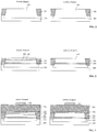
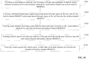
- FIG. 9 illustrates an exemplary fabrication process to form both buried-channel and surface-channel MOSFETs consistent with the disclosed embodiments; and FIGS. 1-9 illustrate semiconductor structures corresponding to certain stages of the exemplary fabrication process.
- FIG. 10 at the beginning of the fabrication process, for both buried-channel and surface-channel MOSFETs, a semiconductor substrate may be provided, and a well area and a plurality of shallow trench isolation structures may be formed in the semiconductor substrate (S101).
- FIG. 1 illustrates a corresponding semiconductor structure.
- a semiconductor substrate 200 (300) may be provided and a well area 203 (303) may be formed in the semiconductor substrate 200 (300).
- the labeling number in the brackets refer to the elements in the surface-channel MOSFET in the figures.
- the semiconductor substrate 200 (300) may include any appropriate semiconductor materials, such as silicon (Si), germanium (Ge), germanium-silicon alloy (GeSi), silicon carbide (SiC), silicon on insulator (SOI), germanium on insulator (GOI), or gallium arsenide (GaAs) and other III-V compounds thereof.
- the semiconductor substrate 200 may be silicon.
- the well area 203 (303) may be formed by performing an ion implantation process onto the semiconductor substrate 200 (300). According to different types of the formed MOSFET, the well area 203 (303) may be doped with different types of impurity ions. Specifically, when the formed MOSFET is an N-type FET, the type of doped impurity ions in the well area may be P-type. The P-type impurity ion may be one or more of boron ion, gallium ion and indium ion. When the formed MOSFET is a P-type FET, the type of doped impurity ions in the well area may be N-type. The N-type impurity ion may be one or more of phosphorus ion, arsenic ion and antimony ion.
- a plurality of shallow trench isolation structures 201 (301) may be formed in the semiconductor substrate 200 (300).
- the shallow trench isolation structures 201 (301) may be configured to isolate the adjacent active areas.
- a fabrication process of the shallow trench isolation structures 201 (301) may include: etching the semiconductor substrate to form notches; and filling the notches with isolation materials to form the shallow trench isolation structures.
- the fabrication process of the shallow trench isolation structures 201 (301) may also include: forming a liner layer on surfaces of both sides and bottom of the notches before filling the notches with isolation materials, and then forming isolation material layer for filling the notches on the liner layer.
- the liner layer can be made of any appropriate material, such as silicon oxide, silicon nitride, or silicon oxynitride, etc.
- the isolation material layer can be made of any appropriate material, such as silicon oxide, silicon oxynitride, or silicon-carbon oxide, etc.
- a threshold implantation region and an anti-punch-through region may be formed in the well area for the buried-channel MOSFET, and an anti-punch-through region may be formed in the well area for the surface-channel MOSFET (S102).
- FIG. 2 illustrates a corresponding semiconductor structure.
- a threshold implantation region 204 may be formed in the well area 203.
- the type of doped impurity ions in the threshold implantation region 204 may be opposite of the type of doped impurity ions in the well area 203 and the depth of the threshold implantation region 204 may be smaller than the depth of the well area 203.
- the threshold implantation region 204 may be formed by an ion implantation process. Before performing the ion implantation process, a mask layer may be formed on the surface of the surface-channel MOSFET.
- the type of doped impurity ions in the threshold implantation region 204 may be opposite of the type of doped impurity ions in the well area 203. Specifically, when the formed MOSFET is an N-type FET, the type of doped impurity ions in the well area 203 may be P-type and the type of doped impurity ions in the threshold implantation region 204 may be N-type.
- the N-type impurity ion may be one or more of phosphorus ion, arsenic ion, and antimony ion.
- the type of doped impurity ions in the well area 203 may be N-type and the type of doped impurity ions in the threshold implantation region 204 may be P-type.
- the P-type impurity ion may be one or more of boron ion, gallium ion, and indium ion.
- the depth of the threshold implantation region 204 may be smaller than the depth of the well area 203.
- the threshold implantation region 204 may be located between the surface of the semiconductor substrate 200 and the bottom of the well area 203.
- the distance between the threshold implantation region 204 and the surface of the semiconductor substrate 200 may be smaller than the distance between the threshold implantation region 204 and the bottom of the well area 203. Therefore, the threshold implantation region 204 may be located inside the semiconductor substrate 200, and both regions above and below the threshold implantation region 204 may be well areas with opposite doping types.
- a PN junction can be formed in the contact area between the threshold implantation region 204 and the well area 203.
- an inversion region can be formed in the area near the PN junction.
- the barrier of the area near the PN junction may be smaller than the barrier of the surface of the semiconductor substrate, carriers can transport in the inversion region formed in the area near the PN junction. Therefore, the transport channel of carriers in MOSFET fabricated with methods in the present invention may be located below the surface of the semiconductor substrate, and the transport of carriers are less affected by defects existed on the surface of the semiconductor substrate, reducing the occurrence of flicker noise and improving the performance of devices.
- the depth of the threshold implantation region 204 is the vertical distance between the bottom of the threshold implantation region 204 and the surface of the semiconductor substrate 200.
- the depth of the well area 203 is the vertical distance between the bottom of the well area 203 and the surface of the semiconductor substrate 200.
- the definition of the depth of the subsequently formed anti-punch-through region and source and drain regions is similar.
- the width of the threshold implantation region 204 may be larger than the width of the subsequently formed gate electrode.
- the method may also include forming an anti-punch-through region 205 (305) in the well area 203 (303).
- the type of doped impurity ions in the anti-punch-through region 205 (305) may be the same as the type of doped impurity ions in the well area 203 (303), and the depth of the anti-punch-through region 205 (305) may be larger than the depth of the threshold implantation region 204 and smaller than the depth of the well area 203 (303).
- the type of doped impurity ions in the well area 203 (303) may be P-type and the type of doped impurity ions in the anti-punch-through region 205 (305) may also be P-type.
- the P-type impurity ion may be one or more of boron ion, gallium ion, and indium ion.
- the type of doped impurity ions in the well area 203 (303) may be N-type and the type of doped impurity ions in the anti-punch-through region 205 (305) may also be N-type.
- the N-type impurity ion may be one or more of phosphorus ion, arsenic ion, and antimony ion.
- a gate structure including a gate dielectric layer and a gate electrode may be formed on the surface of the semiconductor substrate (S103).
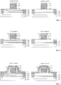
- FIGS. 3 and 4 illustrate the corresponding semiconductor structures.
- a gate structure may be formed on the surface of the semiconductor substrate 200 (300) above the threshold implantation region 204 (the anti-punch-through region 205).
- the gate structure may include a gate dielectric layer 208 (308) and a gate electrode 209 (309) above the gate dielectric layer 208 (308).
- the gate electrode 209 (309) may be doped with impurity ions and the type of doped impurity ions in the gate electrode 209 (309) may be the same as the type of doped impurity ions in the well area 203 (303).
- a fabrication process of forming the gate dielectric layer 208 (308) and the gate electrode 209 (309) may include: forming a gate dielectric material layer 202 (302) on the semiconductor substrate 200 (300); forming a gate electrode material layer 206 (306) on the gate dielectric material layer 202 (302); forming a patterned hard mask layer 207 (307) on the gate electrode material layer 206 (306); and using the patterned hard mask layer 207 (307) as a mask to etch the gate electrode material layer 206 (306) and the gate dielectric material layer 202 (302) to form the gate dielectric layer 208 (308) and the gate electrode 209 (309) on the semiconductor substrate 200 (300).
- the gate dielectric material layer 202 (302) can be made of any appropriate material, such as silicon oxide, silicon nitride, or silicon oxynitride, etc. In one embodiment, the gate dielectric material layer 202 (302) may be made of silicon oxide. The gate dielectric material layer 202 (302) can be formed by a silicon thermal oxidation process, or a chemical vapor deposition process, etc. The gate electrode material layer 206 (306) can be made of any appropriate material, such as polysilicon, or metal, etc. In one embodiment, the gate electrode material layer 206 (306) may be made of polysilicon. The gate electrode material layer 206 (306) may be formed by a chemical vapor deposition process.
- the gate electrode material layer 206 may be doped with impurity ions by an ion implantation process.
- a photoresist layer may be formed on the gate electrode material layer 306 of the surface-channel MOSFET. Therefore, the ion implantation process may be performed only on the gate electrode material layer 206 of the buried-channel MOSFET. In other words, only the gate electrode material layer 206 of the buried-channel MOSFET may be doped with impurity ions.
- the type and concentration of doped impurity ions in the gate electrode material layer 206 may be the type and concentration of doped impurity ions in the subsequently formed gate electrode 209.
- the type of doped impurity ions in the gate electrode 209 may be the same as the type of doped impurity ions in the well area 203. In other words, the type of doped impurity ions in the gate electrode 209 may be opposite of the type of doped impurity ions in the MOSFET. In one embodiment, when a buried-channel N-type MOSFET is formed, a P-type gate electrode may be formed. In another embodiment, when a buried-channel P-type MOSFET is formed, an N-type gate electrode may be formed. It is clearly different from the existing MOSFET, where the type of doped impurity ions in the gate electrode may be the same as the type of doped impurity ions in the MOSFET.
- the threshold implantation region 204 may be formed in the well area 203 at the bottom of the gate electrode.
- the doping type of the threshold implantation region 204 may be opposite of the doping type of the well area 203, such that the existence of the threshold implantation region 204 may have large influence on the threshold voltage of the MOSFET.
- the type of doped impurity ions in the gate electrode 209 may be opposite of the type of doped impurity ions in the threshold implantation region 204 (or the same as the type of doped impurity ions in the well area 203).
- the threshold voltage of the formed MOSFET can be adjusted.
- either the surface-channel or the buried-channel MOSFET of the same type (e.g., NMOS or PMOS) may be formed by using the combination of different gate-electrode doping type and threshold implant doping type and dose.
- the concentration of doped impurity ions in the gate electrode 209 may be positively correlated with the concentration of doped impurity ions in the threshold implantation region 204. That is, the larger the concentration of doped impurity ions in the threshold implantation region 204, the larger the concentration of doped impurity ions in the gate electrode 209.
- the patterned hard mask layer 207 (307) may have a single layer or multilayer ( ⁇ 2 layers) stacked structure and be made of any appropriate material, such as silicon nitride, silicon oxynitride, or silicon carbide, etc.
- FIG. 5 illustrates a corresponding semiconductor structure.
- the sidewall spacers 210 may be formed on both side surfaces of the gate electrode 209 (309) and the gate dielectric layer 208 (308).
- a fabrication process of forming the sidewall spacers 210 (310) may include: forming a sidewall spacer material layer covering the surface of the semiconductor substrate, both side surfaces of the gate electrode 209 (309) and the gate dielectric layer 208 (308), and the side and top surfaces of the patterned hard mask layer 207 (307); and etching the sidewall spacer material layer by a maskless plasma etching process to form sidewall spacers 210 (310) on both side surfaces of the gate electrode 209 (309) and the gate dielectric layer 208 (308).
- the sidewall spacers 210 (310) may also cover both side surfaces of the patterned hard mask layer 207 (307).
- the sidewall spacers 210 (310) may be a part of the gate structure.
- the sidewall spacers 210 (310) may be made of any appropriate materials, such as silicon oxide, silicon nitride, silicon oxynitride, or silicon nitride carbide, etc.
- the sidewall spacers 210 (310) may have a single layer or multilayer ( ⁇ 2 layers) stacked structure.
- the sidewall spacers 210 (310) may have a two-layer stacked structure, including first sidewall spacers formed on both side surfaces of the gate electrode 209 (309) and the gate dielectric layer 208 (308), and second sidewall spacers formed on the surfaces of the first sidewall spacers.
- the first sidewall spacers and the second sidewall spacers may be made of different materials.
- a source region and a drain region may be formed in the semiconductor substrate at both sides of the gate structure (S105).
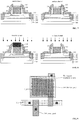
- FIGS. 6-8 illustrate the corresponding semiconductor structures.
- a source region and a drain region may be formed in the semiconductor substrate at both sides of the gate structure.
- the type of doped impurity ions in the source and drain regions may be opposite of the type of doped impurity ions in the well area and the depth of the source and drain regions may be smaller than the depth of the well area and larger than the depth of the threshold implantation region.
- a fabrication process of forming the source and drain regions may include: forming a semiconductor material layer 211 (311) covering the semiconductor substrate, the gate structure and the patterned hard mask layer 207 (307) above the gate structure; etching the semiconductor material layer 211 (311) formed on the surface of the patterned hard mask layer 207 (307) and portions of the semiconductor material layer 211 (311) formed on the semiconductor substrate 200 (300); forming source and drain material layer 213 (313) on the surfaces of the sidewall spacers 210 (310) and the surface of the semiconductor substrate 200 (300) at both sides of the sidewall spacers 210 (310); and forming the source and drain regions by performing an ion implantation process on the source and drain material layer 213 (313) and the semiconductor substrate 200 (300) at both sides of the sidewall spacers 210 (310).
- the source and drain regions may include the source and drain material layer 213 (313) doped with impurity ions on the surfaces of the sidewall spacers 210 (310) and the surface of the semiconductor substrate 200 (300) at both sides of the sidewall spacers 210 (310) and doping regions 212 (312) in the semiconductor substrate 200 (300) at both sides of the sidewall spacers 210 (310).
- the semiconductor material layer 211 (311) may be made of any appropriate material, such as polysilicon, silicon germanium, or silicon carbide, etc.
- the patterned hard mask layer 207 (307) may be removed.
- a photoresist layer 220 may be formed on the gate electrode 209 of the buried-channel MOSFET. Therefore, the gate electrode 209 of the buried-channel MOSFET may not be doped when performing the ion implantation process; and the gate electrode 309 of the surface-channel MOSFET may be doped when performing the ion implantation process.
- the buried-channel MOSFET and the surface-channel MOSFET of the same type e.g. NMOS or PMOS
- different gate electrodes e.g. P-type gate electrode for buried-channel NMOS and N-type gate electrode for surface-channel NMOS
- the gate electrode of the buried-channel MOSFET may also be configured as a floating-gate material for forming a floating-gate memory (pFlash).
- Fig. 9 illustrates a schematic of forming the floating-gate memory with the gate electrode or material of the gate electrode of the buried-channel MOSFET as a floating-gate material.
- the gate electrode of the buried-channel MOSFET may be configured as the floating gate
- the gate electrode of the surface-channel MOSFET may be configured as the select gate.
- the floating gate may be doped by an ion implantation process, and the floating gate implantation area may be larger than the floating gate area.
- the floating gate and the select gate may be electrically isolated from each other through a dielectric layer.
- the select gate may be configured to apply a voltage, and the floating gate may be floated.
- the select gate when an elevated voltage is applied on the select gate, electrons may flow from the source region to the drain region of the surface-channel MOSFET.
- the source to drain current of the surface-channel MOSFET is sufficiently high, high level electrons may punch through the insulating layer and get stuck in the floating gate of the buried-channel MOSFET. Because the floating gate of the buried-channel MOSFET is electrically isolated, charges trapped in the floating gate may be retained for long periods of time.
- the buried-channel MOSFET and the surface-channel MOSFET may need to be arranged on the wafer to form a CMOS device.
- the n-type and p-type buried-channel MOSFETs may be alternatively arranged in one row; and the n-type and p-type surface-channel MOSFETs may be alternatively arranged in one row.
- the n-type buried-channel MOSFET and the p-type surface-channel MOSFET may be arranged in one column; and the p-type buried-channel MOSFET and the n-type surface-channel MOSFET may be arranged in one column.
- Other arrangements may also be used.
- the source and drain regions of the buried-channel MOSFET may include the source and drain material layer 213 (313) doped with impurity ions on the surfaces of the sidewall spacers 210 (310), the surface of the semiconductor substrate 200 (300) at both sides of the sidewall spacers 210 (310), and the doping regions 212 (312) contacting with the source and drain material layer in the semiconductor substrate 200 (300) at both sides of the sidewall spacers 210 (310).
- the source and drain material layer 213 (313) may provide sufficient contact space for subsequently formed metal plugs electrically connected with the source and drain regions and provide sufficient carriers for the conduction of the MOSFET.
- the lateral dimensions of the source and drain regions occupied on the semiconductor substrate in the MOSFET consistent with the disclosed embodiments may be relatively smaller than the lateral dimensions of the source and drain regions occupied in the existing MOSFET, which can improve the integration of devices.
- the source and drain material layer 213 (313) can extend over the shallow trench isolation region 201 (301), allowing for electrical contacts to the source and drain regions to be made over the isolation, improving the packing density of the transistors.
- the source and drain material layer 213 (313) may extend over the isolation to adjacent source or drain regions of transistors, allowing a local interconnect layer which also improves the packing density of the transistors.
- the depth of the doping regions 212 (312) may be larger than the depth of the threshold implantation region 204 and smaller than the depth of the anti-punch-through region 205 (305) and the well area 203 (303).
- the photoresist layer 220 formed on the gate electrode 209 of the buried-channel MOSFET may be removed.
- the fabrication process of the source and drain regions may also include: forming a dielectric layer covering the semiconductor substrate 200 (300), the source and drain regions and the gate structure; and forming metal plugs electrically connected with the source and drain regions and the gate electrode 209 (309), respectively, in the dielectric layer.
- the buried-channel MOSFET may include a semiconductor substrate 200, a well area 203 and a plurality of shallow trench isolation structures in the semiconductor substrate.
- the buried-channel MOSFET may also include a threshold implantation region 204 formed in the well area 203.
- the type of doped impurity ions in the threshold implantation region 204 may be opposite of the type of doped impurity ions in the well area 203 and the depth of the threshold implantation region 204 may be smaller than the depth of the well area 203.
- the buried-channel MOSFET may include a gate structure formed on the surface of the semiconductor substrate 200 above the threshold implantation region 204.
- the gate structure may include a gate dielectric layer 208 and a gate electrode 209 above the gate dielectric layer 208.
- the gate electrode 209 may be doped with impurity ions and the type of doped impurity ions in the gate electrode 209 may be the same as the type of doped impurity ions in the well area 203.
- the buried-channel MOSFET may also include a source region and a drain region formed in the semiconductor substrate at both sides of the gate structure.
- the type of doped impurity ions in the source and drain regions may be opposite of the type of doped impurity ions in the well area and the depth of the source and drain regions may be smaller than the depth of the well area and larger than the depth of the threshold implantation region.
- the gate structure may also include sidewall spacers 210 formed at both side surfaces of the gate dielectric layer 208 and the gate electrode 209.
- the source and drain regions may include the source and drain material layers 213 doped with impurity ions on the surfaces of the sidewall spacers 210 and the surface of the semiconductor substrate 200 at both sides of the sidewall spacers 210, and doping regions 212 contacting with the source and drain material layers in the semiconductor substrate 200 at both sides of the sidewall spacers 210.
- the formed buried-channel MOSFET may be an N-type FET
- the type of doped impurity ions in the well area may be P-type
- the type of doped impurity ions in the threshold implantation region may be N-type
- the type of doped impurity ions in the gate electrode may be P-type
- the type of doped impurity ions in the source and drain regions may be N-type.
- the formed buried-channel MOSFET may be a P-type FET
- the type of doped impurity ions in the well area may be N-type
- the type of doped impurity ions in the threshold implantation region may be P-type
- the type of doped impurity ions in the gate electrode may be N-type
- the type of doped impurity ions in the source and drain regions may be P-type.
- the surface-channel MOSFET may include a semiconductor substrate 300, a well area 303 and a plurality of shallow trench isolation structures in the semiconductor substrate.
- the surface-channel MOSFET may also include a gate structure formed on the surface of the semiconductor substrate 300.
- the gate structure may include a gate dielectric layer 308 and a gate electrode 309 above the gate dielectric layer 308.
- the surface-channel MOSFET may include a source region and a drain region formed in the semiconductor substrate at both sides of the gate structure.
- the gate electrode 309 and the source and drain regions may be doped with impurity ions by the same ion implantation process, and the type of doped impurity ions may be opposite to the type of doped impurity ions in the well area 303.
- the gate structure may also include sidewall spacers 310 formed at both side surfaces of the gate dielectric layer 308 and the gate electrode 309.
- the source and drain regions may include the source and drain material layers 313 doped with impurity ions on the surfaces of the sidewall spacers 310 and on the surface of the semiconductor substrate 300 at both sides of the sidewall spacers 310, and doping regions 312 contacting with the source and drain material layers 313 in the semiconductor substrate 300 at both sides of the sidewall spacers 310.
- the formed surface-channel MOSFET may be an N-type FET
- the type of doped impurity ions in the well area may be P-type
- the type of doped impurity ions in the gate electrode may be N-type
- the type of doped impurity ions in the source and drain regions may be N-type.
- the formed surface-channel MOSFET may be a P-type FET
- the type of doped impurity ions in the well area may be N-type
- the type of doped impurity ions in the gate electrode may be P-type
- the type of doped impurity ions in the source and drain regions may be P-type.
Landscapes
- Engineering & Computer Science (AREA)
- Manufacturing & Machinery (AREA)
- Metal-Oxide And Bipolar Metal-Oxide Semiconductor Integrated Circuits (AREA)
- Insulated Gate Type Field-Effect Transistor (AREA)
- Chemical & Material Sciences (AREA)
- Crystallography & Structural Chemistry (AREA)
Abstract
Description
- This application claims the priority of Chinese patent application No.
201511021410.5, filed on December 30, 2015 - The present invention generally relates to the field of semiconductor manufacturing and, more particularly, relates to a buried-channel MOSFET and a surface-channel MOSFET of a same type, and fabrication method of the MOSFETs.
- The metal-oxide-semiconductor (MOS) field-effect transistor (FET) is the fundamental device in semiconductor manufacturing and has been widely used in various types of integrated circuit. Based on the type of main carriers and doping type during fabrication, FETs can be divided into two types: NMOS FET and PMOS FET. The main carriers in NMOS FETs are electrons and the main carriers in PMOS FETs are holes.
- The existing techniques provide a method for fabricating MOSFET. The method includes providing a semiconductor substrate, and forming isolation structures on the semiconductor substrate. The semiconductor substrate between isolation structures has active areas; and well areas are formed in the active areas (not labeled). The method also includes doping the surface of the well areas with impurity ions by a first ion implantation process to adjust the threshold voltage of the subsequently formed MOSFET; sequentially forming a gate dielectric layer and a gate electrode on the semiconductor substrate between the isolation structures, where the gate dielectric layer and the gate electrode constitute a gate structure; forming an oxide layer covering the gate structure by an oxidation process; and forming source and drain extension regions in the semiconductor substrate at both sides of the gate structure by a shallow ion implantation process. Further, the method includes using the gate structure as a mask to perform a deep ion implantation process in the well areas at both sides of the gate structure, where the energy and dose of the deep ion implantation is larger than the energy and dose of the shallow ion implantation; and forming a source region and a drain region in the well areas at both sides of the gate structure, where the depth of the source and drain regions is larger than the depth of the source and drain extension regions.
- However, the performance of such MOSFET fabricated with existing techniques needs to be improved. The disclosed device structures and methods are directed to solve one or more problems set forth above and other problems.
- A first aspect of the present invention includes a method for fabricating a buried-channel metal-oxide-semiconductor field-effect transistor (MOSFET) and a surface-channel metal-oxide-semiconductor field-effect transistor (MOSFET) of the same type and different gate electrodes on a same wafer, including: providing a semiconductor substrate for each buried-channel and surface-channel MOSFETs; forming a well area and a plurality of shallow trench isolation structures in the semiconductor substrate for each buried-channel and surface-channel MOSFETs; forming a threshold implantation region in the well area for the buried-channel MOSFET, wherein a type of doped impurity ions in the threshold implantation region is opposite of a type of doped impurity ions in the well area, and a depth of the threshold implantation region is smaller than a depth of the well area; forming a gate structure on a surface of the semiconductor substrate for each buried-channel and surface-channel MOSFETs, wherein the gate structure includes a gate dielectric layer and a gate electrode above the gate dielectric layer, the gate electrode of the buried-channel MOSFET is doped with impurity ions and a type of doped impurity ions in the gate electrode of the buried-channel MOSFET is the same as the type of doped impurity ions in the well area, and a type of doped impurity ions in the gate electrode of the surface-channel MOSFET is opposite of the type of doped impurity ions in the well area; and forming a source region and a drain region in the semiconductor substrate at both sides of the gate structure for each buried-channel and surface-channel MOSFETs, wherein a type of doped impurity ions in the source and drain regions is opposite of the type of doped impurity ions in the well area, and a depth of the source and drain regions is smaller than the depth of the well area and larger than the depth of the threshold implantation region.
- In one particular embodiment, the buried-channel MOSFET and surface-channel MOSFET are N-type FETs, wherein: the type of doped impurity ions in the well area for each buried-channel and surface-channel MOSFETs is P-type; the type of doped impurity ions in the threshold implantation region for the buried-channel MOSFET is N-type; the type of doped impurity ions in the source and drain regions for each buried-channel and surface-channel MOSFETs is N-type; the type of doped impurity ions in the gate electrode for the buried-channel MOSFET is P-type; and the type of doped impurity ions in the gate electrode for the surface-channel MOSFET is N-type.
- In an alternative particular embodiment, the buried-channel MOSFET and surface-channel MOSFET are P-type FETs, wherein: the type of doped impurity ions in the well area for each buried-channel and surface-channel MOSFETs is N-type; the type of doped impurity ions in the threshold implantation region for the buried-channel MOSFET is P-type; the type of doped impurity ions in the source and drain regions for each buried-channel and surface-channel MOSFETs is P-type; the type of doped impurity ions in the gate electrode for the buried-channel MOSFET is N-type; and the type of doped impurity ions in the gate electrode for the surface-channel MOSFET is P-type.
- Preferably, the N-type impurity ion is one or more of phosphorus ion, arsenic ion, and antimony ion.
- Preferably, the P-type impurity ion is one or more of boron ion, gallium ion, and indium ion.
- Preferably, the threshold implantation region of the buried-channel MOSFET is formed by an ion implantation process.
- Preferably, the threshold implantation region of the buried-channel MOSFET is located inside the semiconductor substrate, and both regions above and below the threshold implantation region are well areas with opposite doping types to the threshold implantation region, wherein a PN junction is formed in the contact area between the threshold implantation region and the well area, and wherein an inversion region is formed in the area near the PN junction when an operating voltage is applied onto the gate electrode.
- Preferably, a width of the threshold implantation region of the buried-channel MOSFET is larger than a width of the gate electrode.
- Forming the gate structure of the buried-channel and surface-channel MOSFETs may further include: forming a gate dielectric material layer on a surface of the semiconductor substrate; forming a gate electrode material layer on a surface of the gate dielectric material layer, wherein the gate electrode material layer of the buried-channel MOSFET is doped with impurity ions by an ion implantation process; forming a patterned hard mask layer on a surface of the gate electrode material layer; using the patterned hard mask layer as a mask to etch the gate electrode material layer and the gate dielectric material layer; and forming the gate dielectric layer and the gate electrode on the surface of the semiconductor substrate.
- Preferably, a photoresist layer is formed on the gate electrode material layer of the surface-channel MOSFET before performing the ion implantation process. Preferably, the photoresist layer is removed after performing the ion implantation process.
- Forming the buried-channel and surface-channel MOSFETs may further include: forming an anti-punch-through region in the well area, wherein a type of doped impurity ions in the anti-punch-through region is the same as the type of doped impurity ions in the well area, and a depth of the anti-punch-through region is larger than the depth of the threshold implantation region and smaller than the depth of the well area.
- Forming the buried-channel and surface-channel MOSFETs may further include: forming sidewall spacers on both side surfaces of the gate electrode and the gate dielectric layer. Preferably, the gate structure for each buried-channel and surface-channel MOSFETs also includes sidewall spacers at both side surfaces of the gate dielectric layer and the gate electrode.
- Forming the source and drain regions of the buried-channel and surface-channel MOSFETs may further include: forming a semiconductor material layer covering the semiconductor substrate, the gate structure and the patterned hard mask layer above the gate structure; removing the semiconductor material layer on a surface of the patterned hard mask layer and portions of the semiconductor material layer on the semiconductor substrate by an etching process; forming source and drain material layers on surfaces of the sidewall spacers and on the surface of the semiconductor substrate at both sides of the sidewall spacers; removing the patterned hard mask layer; forming a photoresist layer on the gate electrode of the buried-channel MOSFET; and forming the source and drain regions by performing an ion implantation process on the source and drain material layers and the semiconductor substrate at both sides of the sidewall spacers.
- Preferably, the semiconductor material layer is made of polysilicon, silicon germanium, or silicon carbide.
- Preferably, the gate electrode of the buried-channel MOSFET is configured for forming a floating-gate memory.
- A second aspect of the present invention includes a buried-channel MOSFET and a surface-channel MOSFET of a same type and different gate electrodes on a same wafer, comprising: a semiconductor substrate having a well area and a plurality of shallow trench isolation structures for each buried-channel and surface-channel MOSFETs; a threshold implantation region formed in the well area of the buried-channel MOSFET, wherein a type of doped impurity ions in the threshold implantation region of the buried-channel MOSFET is opposite of a type of doped impurity ions in the well area and a depth of the threshold implantation region is smaller than a depth of the well area; a gate structure formed on a surface of the semiconductor substrate for each buried-channel and surface-channel MOSFETs, wherein the gate structure includes a gate dielectric layer and a gate electrode above the gate dielectric layer, the gate electrode of the buried-channel MOSFET is doped with impurity ions and a type of doped impurity ions in the gate electrode of the buried-channel MOSFET is the same as the type of doped impurity ions in the well area, and a type of doped impurity ions in the gate electrode of the surface-channel MOSFET is opposite of the type of doped impurity ions in the well area; and a source region and a drain region formed in the semiconductor substrate at both sides of the gate structure for each buried-channel and surface-channel MOSFETs, wherein a type of doped impurity ions in the source and drain regions is opposite of the type of doped impurity ions in the well area and a depth of the source and drain regions is smaller than the depth of the well area and larger than the depth of the threshold implantation region.
- Preferably, the source and drain regions include a semiconductor material layer above the semiconductor substrate and doping regions in the semiconductor substrate at both sides of the gate structure.
- In a particular embodiment, the buried-channel MOSFET and surface-channel MOSFET are N-type FETs, wherein: the type of doped impurity ions in the well area for each buried-channel and surface-channel MOSFETs is P-type; the type of doped impurity ions in the threshold implantation region for the buried-channel MOSFET is N-type; the type of doped impurity ions in the source and drain regions for each buried-channel and surface-channel MOSFETs is N-type; the type of doped impurity ions in the gate electrode for the buried-channel MOSFET is P-type; the type of doped impurity ions in the gate electrode for the surface-channel MOSFET is N-type;
- In an alternative particular embodiment, the buried-channel MOSFET and surface-channel MOSFET are P-type FETs, wherein: the type of doped impurity ions in the well area for each buried-channel and surface-channel MOSFETs is N-type; the type of doped impurity ions in the threshold implantation region for the buried-channel MOSFET is P-type; the type of doped impurity ions in the source and drain regions for each buried-channel and surface-channel MOSFETs is P-type; the type of doped impurity ions in the gate electrode for the buried-channel MOSFET is N-type; and the type of doped impurity ions in the gate electrode for the surface-channel MOSFET is P-type.
- The buried-channel and surface-channel MOSFETs may further include: an anti-punch-through region formed in the well area, where a type of doped impurity ions in the anti-punch-through region is the same as the type of doped impurity ions in the well area, and a depth of the anti-punch-through region is larger than the depth of the threshold implantation region and is smaller than the depth of the well area.
- Other aspects of the present invention can be understood by those skilled in the art in light of the description, the claims, and the drawings of the present invention.
-
-
FIGS. 1-8 each illustrates semiconductor structures corresponding to a certain stage of a fabrication process of a buried-channel MOSFET and a surface-channel MOSFET consistent with the disclosed embodiments; -
Fig. 9 illustrates a schematic of forming a floating-gate memory with a gate electrode of a buried-channel MOSFET as a floating-gate material; and -
FIG. 10 illustrates an exemplary fabrication process of a buried-channel MOSFET and a surface-channel MOSFET consistent with the disclosed embodiments. - As explained in the background section, the performance of MOSFET fabricated with existing techniques needs to be improved. For example, the existing transistor has flicker noise (1/f noise) or random telegraph noise (RTN) during operation. The occurrence of the flicker noise (1/f noise) or random telegraph noise (RTN) is largely related to charge trapping/de-trapping from near-surface traps, which affects the threshold voltage of the device locally and causes current fluctuations, and is also related to the surface smoothness of the conducting channel, which significantly affects mobility. The conducting channel in existing MOSFET is substantially the surface channel. In the fabrication process, it is hard to ensure the charge traps and smoothness of the substrate surface, and defects may inevitably exist on the substrate surface. The presence of defects can affect the carrier transport and, therefore, when such existing MOSFET is in operation, the flicker noise or the random telegraph noise can appear and the noise performance of MOSFET is affected.
- According to the disclosed device structures and methods, the conducting channel charge traps and smoothness issues and the other issues may be overcome by making a buried-channel to avoid the influence of defects on the semiconductor substrate. The buried channel device reduces the susceptibility to variation from the traps, and also affects mobility.
- In many electronic circuit applications, both digital circuits and analog circuits are present, so as to form a mixed-signal circuit. The surface-channel MOSFET may be configured to optimize the performance of digital circuits (e.g., switching speed), and the buried-channel MOSFET may be configured to optimize the noise performance of certain analog circuits. Therefore, forming both the surface-channel and buried-channel MOSFETs of the same type is desirable in such mixed-signal circuit.
- In the existing techniques, different channel implantations may be performed to form the surface-channel and buried-channel MOSFETs. Therefore, the conducting region in the buried-channel MOSFET is kept away from the surface. In addition, different gate materials (with different work function) may be provided to form the surface-channel and buried-channel MOSFETs. By providing gate materials with different work function, parameters, such as threshold voltage, and saturation current, etc., of the buried-channel and surface-channel MOSFETs can be easily optimized, respectively.
- When polysilicon gate electrodes are used to form the MOSFET, the gate work function is set by the gate doping. The gate doping is usually either done by simultaneously implanting the gate and the source and drain regions of the transistor with one dopant type, or by doping the gate electrode material layer, and then doping the source and drain regions of the transistor by an ion implantation process after patterning the gate electrode. In both cases, the gate doping type for both surface-channel and buried-channel MOSFETs is the same (e.g., either p-type or n-type).
- It is desirable to separate the doping of the gate and the doping of the source and drain regions, thus p-type gate and n-type gate can be formed for the same type of transistor (e.g., either NMOS or PMOS). Therefore, the performance of the digital circuit can be improved by using the surface-channel MOSFET, and the noise performance of the analog circuit can be improved by using the buried-channel MOSFET. In addition, the packing density of transistors is a key factor in circuit size and manufacturing cost. Therefore, it is desirable to improve packing density for the circuits.
- Reference will now be made in detail to exemplary embodiments of the invention, which are illustrated in the accompanying drawings. Wherever possible, the same reference numbers will be used throughout the drawings to refer to the same or the alike parts.
- The present invention provides a buried-channel MOSFET and a surface-channel MOSFET of the same type and different gate electrodes on the same wafer.
FIG. 9 illustrates an exemplary fabrication process to form both buried-channel and surface-channel MOSFETs consistent with the disclosed embodiments; andFIGS. 1-9 illustrate semiconductor structures corresponding to certain stages of the exemplary fabrication process. - As shown in
FIG. 10 , at the beginning of the fabrication process, for both buried-channel and surface-channel MOSFETs, a semiconductor substrate may be provided, and a well area and a plurality of shallow trench isolation structures may be formed in the semiconductor substrate (S101).FIG. 1 illustrates a corresponding semiconductor structure. - Referring to
FIG. 1 , for a buried-channel MOSFET (a surface-channel MOSFET), a semiconductor substrate 200 (300) may be provided and a well area 203 (303) may be formed in the semiconductor substrate 200 (300). For illustrative purposes, the labeling number in the brackets refer to the elements in the surface-channel MOSFET in the figures. - The semiconductor substrate 200 (300) may include any appropriate semiconductor materials, such as silicon (Si), germanium (Ge), germanium-silicon alloy (GeSi), silicon carbide (SiC), silicon on insulator (SOI), germanium on insulator (GOI), or gallium arsenide (GaAs) and other III-V compounds thereof. In one embodiment, the
semiconductor substrate 200 may be silicon. - For the buried-channel MOSFET (the surface-channel MOSFET), the well area 203 (303) may be formed by performing an ion implantation process onto the semiconductor substrate 200 (300). According to different types of the formed MOSFET, the well area 203 (303) may be doped with different types of impurity ions. Specifically, when the formed MOSFET is an N-type FET, the type of doped impurity ions in the well area may be P-type. The P-type impurity ion may be one or more of boron ion, gallium ion and indium ion. When the formed MOSFET is a P-type FET, the type of doped impurity ions in the well area may be N-type. The N-type impurity ion may be one or more of phosphorus ion, arsenic ion and antimony ion.
- Further, as shown in
FIG. 1 , a plurality of shallow trench isolation structures 201 (301) may be formed in the semiconductor substrate 200 (300). The shallow trench isolation structures 201 (301) may be configured to isolate the adjacent active areas. In one embodiment, a fabrication process of the shallow trench isolation structures 201 (301) may include: etching the semiconductor substrate to form notches; and filling the notches with isolation materials to form the shallow trench isolation structures. - In another embodiment, the fabrication process of the shallow trench isolation structures 201 (301) may also include: forming a liner layer on surfaces of both sides and bottom of the notches before filling the notches with isolation materials, and then forming isolation material layer for filling the notches on the liner layer. The liner layer can be made of any appropriate material, such as silicon oxide, silicon nitride, or silicon oxynitride, etc. The isolation material layer can be made of any appropriate material, such as silicon oxide, silicon oxynitride, or silicon-carbon oxide, etc.
- Returning to
FIG. 10 , after forming the well area and the shallow trench isolation structures in the semiconductor substrate, a threshold implantation region and an anti-punch-through region may be formed in the well area for the buried-channel MOSFET, and an anti-punch-through region may be formed in the well area for the surface-channel MOSFET (S102).FIG. 2 illustrates a corresponding semiconductor structure. - Referring to
FIG. 2 , for the buried-channel MOSFET, athreshold implantation region 204 may be formed in thewell area 203. The type of doped impurity ions in thethreshold implantation region 204 may be opposite of the type of doped impurity ions in thewell area 203 and the depth of thethreshold implantation region 204 may be smaller than the depth of thewell area 203. - The
threshold implantation region 204 may be formed by an ion implantation process. Before performing the ion implantation process, a mask layer may be formed on the surface of the surface-channel MOSFET. The type of doped impurity ions in thethreshold implantation region 204 may be opposite of the type of doped impurity ions in thewell area 203. Specifically, when the formed MOSFET is an N-type FET, the type of doped impurity ions in thewell area 203 may be P-type and the type of doped impurity ions in thethreshold implantation region 204 may be N-type. The N-type impurity ion may be one or more of phosphorus ion, arsenic ion, and antimony ion. When the formed MOSFET is a P-type FET, the type of doped impurity ions in thewell area 203 may be N-type and the type of doped impurity ions in thethreshold implantation region 204 may be P-type. The P-type impurity ion may be one or more of boron ion, gallium ion, and indium ion. - As shown in
FIG. 2 , the depth of thethreshold implantation region 204 may be smaller than the depth of thewell area 203. Thethreshold implantation region 204 may be located between the surface of thesemiconductor substrate 200 and the bottom of thewell area 203. The distance between thethreshold implantation region 204 and the surface of thesemiconductor substrate 200 may be smaller than the distance between thethreshold implantation region 204 and the bottom of thewell area 203. Therefore, thethreshold implantation region 204 may be located inside thesemiconductor substrate 200, and both regions above and below thethreshold implantation region 204 may be well areas with opposite doping types. A PN junction can be formed in the contact area between thethreshold implantation region 204 and thewell area 203. - After subsequently forming a gate electrode, when an operating voltage is applied onto the gate electrode, an inversion region can be formed in the area near the PN junction. Because the barrier of the area near the PN junction may be smaller than the barrier of the surface of the semiconductor substrate, carriers can transport in the inversion region formed in the area near the PN junction. Therefore, the transport channel of carriers in MOSFET fabricated with methods in the present invention may be located below the surface of the semiconductor substrate, and the transport of carriers are less affected by defects existed on the surface of the semiconductor substrate, reducing the occurrence of flicker noise and improving the performance of devices.
- In the present invention, the depth of the
threshold implantation region 204 is the vertical distance between the bottom of thethreshold implantation region 204 and the surface of thesemiconductor substrate 200. The depth of thewell area 203 is the vertical distance between the bottom of thewell area 203 and the surface of thesemiconductor substrate 200. The definition of the depth of the subsequently formed anti-punch-through region and source and drain regions is similar. The width of thethreshold implantation region 204 may be larger than the width of the subsequently formed gate electrode. After forming thethreshold implantation region 204 for the buried-channel MOSFET, the mask layer formed on the surface of the surface-channel MOSFET may be removed. - Further, as shown in
FIG. 2 , for the buried-channel MOSFET (surface-channel MOSFET), before forming a gate dielectric layer and a gate electrode, the method may also include forming an anti-punch-through region 205 (305) in the well area 203 (303). The type of doped impurity ions in the anti-punch-through region 205 (305) may be the same as the type of doped impurity ions in the well area 203 (303), and the depth of the anti-punch-through region 205 (305) may be larger than the depth of thethreshold implantation region 204 and smaller than the depth of the well area 203 (303). - In one embodiment, when the formed MOSFET is an N-type FET, the type of doped impurity ions in the well area 203 (303) may be P-type and the type of doped impurity ions in the anti-punch-through region 205 (305) may also be P-type. The P-type impurity ion may be one or more of boron ion, gallium ion, and indium ion. In another embodiment, when the formed MOSFET is P-type FET, the type of doped impurity ions in the well area 203 (303) may be N-type and the type of doped impurity ions in the anti-punch-through region 205 (305) may also be N-type. The N-type impurity ion may be one or more of phosphorus ion, arsenic ion, and antimony ion.
- Returning to
FIG. 10 , for both buried-channel and surface-channel MOSFETs, after forming the threshold implantation region and/or the anti-punch-through region, a gate structure including a gate dielectric layer and a gate electrode may be formed on the surface of the semiconductor substrate (S103).FIGS. 3 and4 illustrate the corresponding semiconductor structures. - Referring to
FIGS. 3 and4 , for the buried-channel MOSFET (surface-channel MOSFET), a gate structure may be formed on the surface of the semiconductor substrate 200 (300) above the threshold implantation region 204 (the anti-punch-through region 205). The gate structure may include a gate dielectric layer 208 (308) and a gate electrode 209 (309) above the gate dielectric layer 208 (308). The gate electrode 209 (309) may be doped with impurity ions and the type of doped impurity ions in the gate electrode 209 (309) may be the same as the type of doped impurity ions in the well area 203 (303). - As shown in
FIG. 3 , for the buried-channel MOSFET (the surface-channel MOSFET), a fabrication process of forming the gate dielectric layer 208 (308) and the gate electrode 209 (309) may include: forming a gate dielectric material layer 202 (302) on the semiconductor substrate 200 (300); forming a gate electrode material layer 206 (306) on the gate dielectric material layer 202 (302); forming a patterned hard mask layer 207 (307) on the gate electrode material layer 206 (306); and using the patterned hard mask layer 207 (307) as a mask to etch the gate electrode material layer 206 (306) and the gate dielectric material layer 202 (302) to form the gate dielectric layer 208 (308) and the gate electrode 209 (309) on the semiconductor substrate 200 (300). - For the buried-channel MOSFET (the surface-channel MOSFET), the gate dielectric material layer 202 (302) can be made of any appropriate material, such as silicon oxide, silicon nitride, or silicon oxynitride, etc. In one embodiment, the gate dielectric material layer 202 (302) may be made of silicon oxide. The gate dielectric material layer 202 (302) can be formed by a silicon thermal oxidation process, or a chemical vapor deposition process, etc. The gate electrode material layer 206 (306) can be made of any appropriate material, such as polysilicon, or metal, etc. In one embodiment, the gate electrode material layer 206 (306) may be made of polysilicon. The gate electrode material layer 206 (306) may be formed by a chemical vapor deposition process.
- For the buried-channel MOSFET, the gate
electrode material layer 206 may be doped with impurity ions by an ion implantation process. Before performing the ion implantation process, a photoresist layer may be formed on the gateelectrode material layer 306 of the surface-channel MOSFET. Therefore, the ion implantation process may be performed only on the gateelectrode material layer 206 of the buried-channel MOSFET. In other words, only the gateelectrode material layer 206 of the buried-channel MOSFET may be doped with impurity ions. The type and concentration of doped impurity ions in the gateelectrode material layer 206 may be the type and concentration of doped impurity ions in the subsequently formedgate electrode 209. - The type of doped impurity ions in the
gate electrode 209 may be the same as the type of doped impurity ions in thewell area 203. In other words, the type of doped impurity ions in thegate electrode 209 may be opposite of the type of doped impurity ions in the MOSFET. In one embodiment, when a buried-channel N-type MOSFET is formed, a P-type gate electrode may be formed. In another embodiment, when a buried-channel P-type MOSFET is formed, an N-type gate electrode may be formed. It is clearly different from the existing MOSFET, where the type of doped impurity ions in the gate electrode may be the same as the type of doped impurity ions in the MOSFET. The purpose to do so in the present invention is that thethreshold implantation region 204 may be formed in thewell area 203 at the bottom of the gate electrode. The doping type of thethreshold implantation region 204 may be opposite of the doping type of thewell area 203, such that the existence of thethreshold implantation region 204 may have large influence on the threshold voltage of the MOSFET. The type of doped impurity ions in thegate electrode 209 may be opposite of the type of doped impurity ions in the threshold implantation region 204 (or the same as the type of doped impurity ions in the well area 203). Thus, the threshold voltage of the formed MOSFET can be adjusted. In addition, either the surface-channel or the buried-channel MOSFET of the same type (e.g., NMOS or PMOS) may be formed by using the combination of different gate-electrode doping type and threshold implant doping type and dose. - The concentration of doped impurity ions in the
gate electrode 209 may be positively correlated with the concentration of doped impurity ions in thethreshold implantation region 204. That is, the larger the concentration of doped impurity ions in thethreshold implantation region 204, the larger the concentration of doped impurity ions in thegate electrode 209. - After doping the gate
electrode material layer 206 of the buried-channel MOSFET with impurity ions, and before forming the patterned hard mask layer 207 (307), the photoresist layer formed on the gateelectrode material layer 306 of the surface-channel MOSFET may be removed. The patterned hard mask layer 207 (307) may have a single layer or multilayer (≥ 2 layers) stacked structure and be made of any appropriate material, such as silicon nitride, silicon oxynitride, or silicon carbide, etc. - Returning to
FIG. 10 , after forming the gate structure including the gate dielectric layer and the gate electrode, for both buried-channel and surface-channel MOSFETs, sidewall spacers may be formed on both side surfaces of the gate electrode and the gate dielectric layer (S104).FIG. 5 illustrates a corresponding semiconductor structure. - Referring to
FIG. 5 , for the buried-channel MOSFET (surface-channel MOSFET), the sidewall spacers 210 (310) may be formed on both side surfaces of the gate electrode 209 (309) and the gate dielectric layer 208 (308). - As shown in
FIG. 5 , for the buried-channel MOSFET (the surface-channel MOSFET), a fabrication process of forming the sidewall spacers 210 (310) may include: forming a sidewall spacer material layer covering the surface of the semiconductor substrate, both side surfaces of the gate electrode 209 (309) and the gate dielectric layer 208 (308), and the side and top surfaces of the patterned hard mask layer 207 (307); and etching the sidewall spacer material layer by a maskless plasma etching process to form sidewall spacers 210 (310) on both side surfaces of the gate electrode 209 (309) and the gate dielectric layer 208 (308). The sidewall spacers 210 (310) may also cover both side surfaces of the patterned hard mask layer 207 (307). - The sidewall spacers 210 (310) may be a part of the gate structure. The sidewall spacers 210 (310) may be made of any appropriate materials, such as silicon oxide, silicon nitride, silicon oxynitride, or silicon nitride carbide, etc.
- The sidewall spacers 210 (310) may have a single layer or multilayer (≥ 2 layers) stacked structure. In one embodiment, the sidewall spacers 210 (310) may have a two-layer stacked structure, including first sidewall spacers formed on both side surfaces of the gate electrode 209 (309) and the gate dielectric layer 208 (308), and second sidewall spacers formed on the surfaces of the first sidewall spacers. The first sidewall spacers and the second sidewall spacers may be made of different materials.
- Returning to
FIG. 10 , after forming the sidewall spacers, for both buried-channel and surface-channel MOSFETs, a source region and a drain region may be formed in the semiconductor substrate at both sides of the gate structure (S105).FIGS. 6-8 illustrate the corresponding semiconductor structures. - Referring to
FIGS. 6-8 , for both buried-channel and surface-channel MOSFETs, a source region and a drain region may be formed in the semiconductor substrate at both sides of the gate structure. The type of doped impurity ions in the source and drain regions may be opposite of the type of doped impurity ions in the well area and the depth of the source and drain regions may be smaller than the depth of the well area and larger than the depth of the threshold implantation region. - In one embodiment, for the buried-channel MOSFET (surface-channel MOSFET), a fabrication process of forming the source and drain regions may include: forming a semiconductor material layer 211 (311) covering the semiconductor substrate, the gate structure and the patterned hard mask layer 207 (307) above the gate structure; etching the semiconductor material layer 211 (311) formed on the surface of the patterned hard mask layer 207 (307) and portions of the semiconductor material layer 211 (311) formed on the semiconductor substrate 200 (300); forming source and drain material layer 213 (313) on the surfaces of the sidewall spacers 210 (310) and the surface of the semiconductor substrate 200 (300) at both sides of the sidewall spacers 210 (310); and forming the source and drain regions by performing an ion implantation process on the source and drain material layer 213 (313) and the semiconductor substrate 200 (300) at both sides of the sidewall spacers 210 (310). The source and drain regions may include the source and drain material layer 213 (313) doped with impurity ions on the surfaces of the sidewall spacers 210 (310) and the surface of the semiconductor substrate 200 (300) at both sides of the sidewall spacers 210 (310) and doping regions 212 (312) in the semiconductor substrate 200 (300) at both sides of the sidewall spacers 210 (310). The semiconductor material layer 211 (311) may be made of any appropriate material, such as polysilicon, silicon germanium, or silicon carbide, etc.
- Referring to
Fig. 8 , for the buried-channel MOSFET (surface-channel MOSFET), after forming the source and drain material layer 213 (313), the patterned hard mask layer 207 (307) may be removed. Before performing the ion implantation process, the source and drain material layer 213 (313) and the semiconductor substrate 200 (300) at both sides of the sidewall spacers 210 (310), aphotoresist layer 220 may be formed on thegate electrode 209 of the buried-channel MOSFET. Therefore, thegate electrode 209 of the buried-channel MOSFET may not be doped when performing the ion implantation process; and thegate electrode 309 of the surface-channel MOSFET may be doped when performing the ion implantation process. Thus, the buried-channel MOSFET and the surface-channel MOSFET of the same type (e.g. NMOS or PMOS) and different gate electrodes (e.g. P-type gate electrode for buried-channel NMOS and N-type gate electrode for surface-channel NMOS) may be formed on the same wafer. - The gate electrode of the buried-channel MOSFET may also be configured as a floating-gate material for forming a floating-gate memory (pFlash).
Fig. 9 illustrates a schematic of forming the floating-gate memory with the gate electrode or material of the gate electrode of the buried-channel MOSFET as a floating-gate material. Referring toFig. 9 , the gate electrode of the buried-channel MOSFET may be configured as the floating gate, and the gate electrode of the surface-channel MOSFET may be configured as the select gate. The floating gate may be doped by an ion implantation process, and the floating gate implantation area may be larger than the floating gate area. The floating gate and the select gate may be electrically isolated from each other through a dielectric layer. The select gate may be configured to apply a voltage, and the floating gate may be floated. For NMOS transistors, when an elevated voltage is applied on the select gate, electrons may flow from the source region to the drain region of the surface-channel MOSFET. When the source to drain current of the surface-channel MOSFET is sufficiently high, high level electrons may punch through the insulating layer and get stuck in the floating gate of the buried-channel MOSFET. Because the floating gate of the buried-channel MOSFET is electrically isolated, charges trapped in the floating gate may be retained for long periods of time. - For constructing integrated circuits, the buried-channel MOSFET and the surface-channel MOSFET may need to be arranged on the wafer to form a CMOS device. In one embodiment, the n-type and p-type buried-channel MOSFETs may be alternatively arranged in one row; and the n-type and p-type surface-channel MOSFETs may be alternatively arranged in one row. At the same time, the n-type buried-channel MOSFET and the p-type surface-channel MOSFET may be arranged in one column; and the p-type buried-channel MOSFET and the n-type surface-channel MOSFET may be arranged in one column. Other arrangements may also be used.
- As shown in
FIG. 7 , in one embodiment, the source and drain regions of the buried-channel MOSFET (surface-channel MOSFET) may include the source and drain material layer 213 (313) doped with impurity ions on the surfaces of the sidewall spacers 210 (310), the surface of the semiconductor substrate 200 (300) at both sides of the sidewall spacers 210 (310), and the doping regions 212 (312) contacting with the source and drain material layer in the semiconductor substrate 200 (300) at both sides of the sidewall spacers 210 (310). Because portions of the source and drain material layer 213 (313) may be formed on the surface of the semiconductor substrate 200 (300) and the other part of the source and drain material layer 213 (313) may be formed on the surfaces of the sidewall spacers 210 (310), the source and drain material layer 213 (313) may provide sufficient contact space for subsequently formed metal plugs electrically connected with the source and drain regions and provide sufficient carriers for the conduction of the MOSFET. The lateral dimensions of the source and drain regions occupied on the semiconductor substrate in the MOSFET consistent with the disclosed embodiments may be relatively smaller than the lateral dimensions of the source and drain regions occupied in the existing MOSFET, which can improve the integration of devices. - As shown in
FIG. 7 , in one embodiment, the source and drain material layer 213 (313) can extend over the shallow trench isolation region 201 (301), allowing for electrical contacts to the source and drain regions to be made over the isolation, improving the packing density of the transistors. In addition, the source and drain material layer 213 (313) may extend over the isolation to adjacent source or drain regions of transistors, allowing a local interconnect layer which also improves the packing density of the transistors. - For the buried-channel MOSFET (surface-channel MOSFET), the depth of the doping regions 212 (312) may be larger than the depth of the
threshold implantation region 204 and smaller than the depth of the anti-punch-through region 205 (305) and the well area 203 (303). After performing the ion implantation process, thephotoresist layer 220 formed on thegate electrode 209 of the buried-channel MOSFET may be removed. - For the buried-channel MOSFET (surface-channel MOSFET), the fabrication process of the source and drain regions may also include: forming a dielectric layer covering the semiconductor substrate 200 (300), the source and drain regions and the gate structure; and forming metal plugs electrically connected with the source and drain regions and the gate electrode 209 (309), respectively, in the dielectric layer.
- Further, a buried-channel MOSFET and a surface-channel MOSFET of the same type and different gate electrodes formed on the same wafer may be provided in the present invention. In one embodiment, as shown in
FIG. 8 , the buried-channel MOSFET may include asemiconductor substrate 200, awell area 203 and a plurality of shallow trench isolation structures in the semiconductor substrate. The buried-channel MOSFET may also include athreshold implantation region 204 formed in thewell area 203. The type of doped impurity ions in thethreshold implantation region 204 may be opposite of the type of doped impurity ions in thewell area 203 and the depth of thethreshold implantation region 204 may be smaller than the depth of thewell area 203. - Further, the buried-channel MOSFET may include a gate structure formed on the surface of the
semiconductor substrate 200 above thethreshold implantation region 204. The gate structure may include agate dielectric layer 208 and agate electrode 209 above thegate dielectric layer 208. Thegate electrode 209 may be doped with impurity ions and the type of doped impurity ions in thegate electrode 209 may be the same as the type of doped impurity ions in thewell area 203. - Further, the buried-channel MOSFET may also include a source region and a drain region formed in the semiconductor substrate at both sides of the gate structure. The type of doped impurity ions in the source and drain regions may be opposite of the type of doped impurity ions in the well area and the depth of the source and drain regions may be smaller than the depth of the well area and larger than the depth of the threshold implantation region.
- The gate structure may also include
sidewall spacers 210 formed at both side surfaces of thegate dielectric layer 208 and thegate electrode 209. The source and drain regions may include the source and drainmaterial layers 213 doped with impurity ions on the surfaces of thesidewall spacers 210 and the surface of thesemiconductor substrate 200 at both sides of thesidewall spacers 210, anddoping regions 212 contacting with the source and drain material layers in thesemiconductor substrate 200 at both sides of thesidewall spacers 210. - In one embodiment, the formed buried-channel MOSFET may be an N-type FET, the type of doped impurity ions in the well area may be P-type, the type of doped impurity ions in the threshold implantation region may be N-type, the type of doped impurity ions in the gate electrode may be P-type, and the type of doped impurity ions in the source and drain regions may be N-type.
- In another embodiment, the formed buried-channel MOSFET may be a P-type FET, the type of doped impurity ions in the well area may be N-type, the type of doped impurity ions in the threshold implantation region may be P-type, the type of doped impurity ions in the gate electrode may be N-type, and the type of doped impurity ions in the source and drain regions may be P-type.
- In one embodiment, as shown in
FIG. 8 , the surface-channel MOSFET may include asemiconductor substrate 300, awell area 303 and a plurality of shallow trench isolation structures in the semiconductor substrate. The surface-channel MOSFET may also include a gate structure formed on the surface of thesemiconductor substrate 300. The gate structure may include agate dielectric layer 308 and agate electrode 309 above thegate dielectric layer 308. Further, the surface-channel MOSFET may include a source region and a drain region formed in the semiconductor substrate at both sides of the gate structure. Thegate electrode 309 and the source and drain regions may be doped with impurity ions by the same ion implantation process, and the type of doped impurity ions may be opposite to the type of doped impurity ions in thewell area 303. - The gate structure may also include
sidewall spacers 310 formed at both side surfaces of thegate dielectric layer 308 and thegate electrode 309. The source and drain regions may include the source and drainmaterial layers 313 doped with impurity ions on the surfaces of thesidewall spacers 310 and on the surface of thesemiconductor substrate 300 at both sides of thesidewall spacers 310, anddoping regions 312 contacting with the source and drainmaterial layers 313 in thesemiconductor substrate 300 at both sides of thesidewall spacers 310. - In one embodiment, the formed surface-channel MOSFET may be an N-type FET, the type of doped impurity ions in the well area may be P-type, the type of doped impurity ions in the gate electrode may be N-type, and the type of doped impurity ions in the source and drain regions may be N-type.
- In another embodiment, the formed surface-channel MOSFET may be a P-type FET, the type of doped impurity ions in the well area may be N-type, the type of doped impurity ions in the gate electrode may be P-type, and the type of doped impurity ions in the source and drain regions may be P-type.
Claims (15)
- A method for fabricating a buried-channel metal-oxide-semiconductor field-effect transistor (MOSFET) and a surface-channel metal-oxide-semiconductor field-effect transistor (MOSFET) of a same type and different gate electrodes on a same wafer, comprising:providing a semiconductor substrate for each buried-channel and surface-channel MOSFETs;forming a well area and a plurality of shallow trench isolation structures in the semiconductor substrate for each buried-channel and surface-channel MOSFETs;forming a threshold implantation region in the well area for the buried-channel MOSFET, wherein a type of doped impurity ions in the threshold implantation region is opposite of a type of doped impurity ions in the well area, and a depth of the threshold implantation region is smaller than a depth of the well area;forming a gate structure on a surface of the semiconductor substrate for each buried-channel and surface-channel MOSFETs, wherein the gate structure includes a gate dielectric layer and a gate electrode above the gate dielectric layer, the gate electrode of the buried-channel MOSFET is doped with impurity ions and a type of doped impurity ions in the gate electrode of the buried-channel MOSFET is the same as the type of doped impurity ions in the well area, and a type of doped impurity ions in the gate electrode of the surface-channel MOSFET is opposite of the type of doped impurity ions in the well area; andforming a source region and a drain region in the semiconductor substrate at both sides of the gate structure for each buried-channel and surface-channel MOSFETs, wherein a type of doped impurity ions in the source and drain regions is opposite of the type of doped impurity ions in the well area, and a depth of the source and drain regions is smaller than the depth of the well area and larger than the depth of the threshold implantation region.
- The method according to claim 1, wherein:the buried-channel MOSFET and surface-channel MOSFET are both N-type FETs or P-type FETs;if the buried-channel MOSFET and surface-channel MOSFET are both N-type FETs: the type of doped impurity ions in the well area for each buried-channel and surface-channel MOSFETs is P-type; the type of doped impurity ions in the threshold implantation region for the buried-channel MOSFET is N-type; the type of doped impurity ions in the source and drain regions for each buried-channel and surface-channel MOSFETs is N-type; the type of doped impurity ions in the gate electrode for the buried-channel MOSFET is P-type; and the type of doped impurity ions in the gate electrode for the surface-channel MOSFET is N-type; orif the buried-channel MOSFET and surface-channel MOSFET are both P-type FETs: the type of doped impurity ions in the well area for each buried-channel and surface-channel MOSFETs is N-type; the type of doped impurity ions in the threshold implantation region for the buried-channel MOSFET is P-type; the type of doped impurity ions in the source and drain regions for each buried-channel and surface-channel MOSFETs is P-type; the type of doped impurity ions in the gate electrode for the buried-channel MOSFET is N-type; and the type of doped impurity ions in the gate electrode for the surface-channel MOSFET is P-type; andwherein preferably the N-type impurity ion is one or more of phosphorus ion, arsenic ion, and antimony ion, and the P-type impurity ion is one or more of boron ion, gallium ion, and indium ion.
- The method according to claim 1 or 2, wherein the method comprises at least one of:forming the threshold implantation region of the buried-channel MOSFET by an ion implantation process;forming a width of the threshold implantation region of the buried-channel MOSFET to be larger than a width of the gate electrode.
- The method according to any one of the claims 1-3, wherein:the threshold implantation region of the buried-channel MOSFET is located inside the semiconductor substrate, and both regions above and below the threshold implantation region are well areas with opposite doping types to the threshold implantation region;a PN junction is formed in the contact area between the threshold implantation region and the well area; andan inversion region is formed in the area near the PN junction when an operating voltage is applied onto the gate electrode.
- The method according to any one of the claims 1-4, wherein forming the gate structure of the buried-channel and surface-channel MOSFETs further includes:forming a gate dielectric material layer on a surface of the semiconductor substrate;forming a gate electrode material layer on a surface of the gate dielectric material layer, wherein the gate electrode material layer of the buried-channel MOSFET is doped with impurity ions by an ion implantation process;forming a patterned hard mask layer on a surface of the gate electrode material layer;using the patterned hard mask layer as a mask to etch the gate electrode material layer and the gate dielectric material layer; andforming the gate dielectric layer and the gate electrode on the surface of the semiconductor substrate; andwherein preferably: a photoresist layer is formed on the gate electrode material layer of the surface-channel MOSFET before performing the ion implantation process; and the photoresist layer is removed after performing the ion implantation process.
- The method according to any one of the claims 1-5, wherein forming the buried-channel and surface-channel MOSFETs further includes: forming an anti-punch-through region in the well area, wherein a type of doped impurity ions in the anti-punch-through region is the same as the type of doped impurity ions in the well area, and a depth of the anti-punch-through region is larger than the depth of the threshold implantation region and smaller than the depth of the well area.
- The method according to any one of the claims 1-6, wherein forming the buried-channel and surface-channel MOSFETs further includes: forming sidewall spacers on both side surfaces of the gate electrode and the gate dielectric layer; and
wherein preferably: the gate structure for each buried-channel and surface-channel MOSFETs also includes sidewall spacers at both side surfaces of the gate dielectric layer and the gate electrode. - The method according to any one of the claims 1-7, wherein forming the source and drain regions of the buried-channel and surface-channel MOSFETs further includes:forming a semiconductor material layer covering the semiconductor substrate, the gate structure and the patterned hard mask layer above the gate structure;removing the semiconductor material layer on a surface of the patterned hard mask layer and portions of the semiconductor material layer on the semiconductor substrate by an etching process;forming source and drain material layers on surfaces of the sidewall spacers and on the surface of the semiconductor substrate at both sides of the sidewall spacers;removing the patterned hard mask layer;forming a photoresist layer on the gate electrode of the buried-channel MOSFET; andforming the source and drain regions by performing an ion implantation process on the source and drain material layers and the semiconductor substrate at both sides of the sidewall spacers.
- The method according to claim 8, wherein:the semiconductor material layer is made of polysilicon, silicon germanium, or silicon carbide.
- The method according to any one of the claims 1-9, wherein:the gate electrode of the buried-channel MOSFET is configured for forming a floating-gate memory.
- A buried-channel MOSFET and a surface-channel MOSFET of a same type and different gate electrodes on a same wafer, comprising:a semiconductor substrate having a well area and a plurality of shallow trench isolation structures for each buried-channel and surface-channel MOSFETs;a threshold implantation region formed in the well area of the buried-channel MOSFET, wherein a type of doped impurity ions in the threshold implantation region of the buried-channel MOSFET is opposite of a type of doped impurity ions in the well area and a depth of the threshold implantation region is smaller than a depth of the well area;a gate structure formed on a surface of the semiconductor substrate for each buried-channel and surface-channel MOSFETs, wherein the gate structure includes a gate dielectric layer and a gate electrode above the gate dielectric layer, the gate electrode of the buried-channel MOSFET is doped with impurity ions and a type of doped impurity ions in the gate electrode of the buried-channel MOSFET is the same as the type of doped impurity ions in the well area, and a type of doped impurity ions in the gate electrode of the surface-channel MOSFET is opposite of the type of doped impurity ions in the well area; anda source region and a drain region formed in the semiconductor substrate at both sides of the gate structure for each buried-channel and surface-channel MOSFETs, wherein a type of doped impurity ions in the source and drain regions is opposite of the type of doped impurity ions in the well area and a depth of the source and drain regions is smaller than the depth of the well area and larger than the depth of the threshold implantation region.
- The buried-channel and surface-channel MOSFETs according to claim 11, wherein:the source and drain regions include a semiconductor material layer above the semiconductor substrate and doping regions in the semiconductor substrate at both sides of the gate structure.
- The buried-channel and surface-channel MOSFETs according to claim 11 or 12, wherein:the buried-channel MOSFET and surface-channel MOSFET are N-type FETs;the type of doped impurity ions in the well area for each buried-channel and surface-channel MOSFETs is P-type;the type of doped impurity ions in the threshold implantation region for the buried-channel MOSFET is N-type;the type of doped impurity ions in the source and drain regions for each buried-channel and surface-channel MOSFETs is N-type;the type of doped impurity ions in the gate electrode for the buried-channel MOSFET is P-type; andthe type of doped impurity ions in the gate electrode for the surface-channel MOSFET is N-type.
- The buried-channel and surface-channel MOSFETs to claim 11 or 12, wherein:the buried-channel MOSFET and surface-channel MOSFET are P-type FETs;the type of doped impurity ions in the well area for each buried-channel and surface-channel MOSFETs is N-type;the type of doped impurity ions in the threshold implantation region for the buried-channel MOSFET is P-type;the type of doped impurity ions in the source and drain regions for each buried-channel and surface-channel MOSFETs is P-type;the type of doped impurity ions in the gate electrode for the buried-channel MOSFET is N-type; andthe type of doped impurity ions in the gate electrode for the surface-channel MOSFET is P-type.
- The buried-channel and surface-channel MOSFETs according to any one of the claims 11-14, further including:an anti-punch-through region formed in the well area, where a type of doped impurity ions in the anti-punch-through region is the same as the type of doped impurity ions in the well area, and a depth of the anti-punch-through region is larger than the depth of the threshold implantation region and is smaller than the depth of the well area.
Applications Claiming Priority (1)
| Application Number | Priority Date | Filing Date | Title |
|---|---|---|---|
| CN201511021410.5A CN106935646B (en) | 2015-12-30 | 2015-12-30 | Buried channel transistor and method of forming the same |
Publications (1)
| Publication Number | Publication Date |
|---|---|
| EP3188226A1 true EP3188226A1 (en) | 2017-07-05 |
Family
ID=57614291
Family Applications (1)
| Application Number | Title | Priority Date | Filing Date |
|---|---|---|---|
| EP16207183.1A Withdrawn EP3188226A1 (en) | 2015-12-30 | 2016-12-28 | A buried-channel mosfet and a surface-channel mosfet of a same type and fabrication method thereof |
Country Status (3)
| Country | Link |
|---|---|
| US (1) | US10062704B2 (en) |
| EP (1) | EP3188226A1 (en) |
| CN (1) | CN106935646B (en) |
Families Citing this family (8)
| Publication number | Priority date | Publication date | Assignee | Title |
|---|---|---|---|---|
| CN110943129A (en) * | 2018-09-25 | 2020-03-31 | 长鑫存储技术有限公司 | Semiconductor device and method for manufacturing the same |
| CN112289686B (en) * | 2019-07-24 | 2022-03-04 | 长鑫存储技术有限公司 | Manufacturing method of semiconductor device and doping method of substrate |
| CN112992663B (en) * | 2019-12-16 | 2022-09-16 | 无锡华润上华科技有限公司 | Manufacturing method of high-voltage CMOS, high-voltage CMOS and electronic device |
| CN111354797B (en) * | 2020-03-12 | 2023-03-10 | 上海华虹宏力半导体制造有限公司 | Radio frequency device and method of forming the same |
| CN113823677B (en) * | 2020-06-18 | 2023-12-26 | 联华电子股份有限公司 | Metal oxide semiconductor field effect transistor with buried gate channel and manufacturing method thereof |
| CN115588694A (en) * | 2022-08-24 | 2023-01-10 | 西安电子科技大学芜湖研究院 | A Silicon Carbide MOSFET Gas Sensor with Buried Channel |
| CN119677145B (en) * | 2023-09-14 | 2026-04-17 | 长江存储科技有限责任公司 | Semiconductor structure, manufacturing method thereof and memory device |
| CN117133793B (en) * | 2023-10-26 | 2024-03-01 | 合肥晶合集成电路股份有限公司 | Semiconductor memory device and manufacturing method thereof |
Citations (5)
| Publication number | Priority date | Publication date | Assignee | Title |
|---|---|---|---|---|
| US5498555A (en) * | 1994-11-07 | 1996-03-12 | United Microelectronics Corporation | Method of making LDD with polysilicon and dielectric spacers |
| US6337248B1 (en) * | 1998-08-28 | 2002-01-08 | Nec Corporation | Process for manufacturing semiconductor devices |
| US20030025165A1 (en) * | 2001-08-01 | 2003-02-06 | Youngmin Kim | Buried channel pmos transistor in dual gate cmos with reduced masking steps |
| US6747318B1 (en) * | 2001-12-13 | 2004-06-08 | Lsi Logic Corporation | Buried channel devices and a process for their fabrication simultaneously with surface channel devices to produce transistors and capacitors with multiple electrical gate oxides |
| US20130221418A1 (en) * | 2012-02-28 | 2013-08-29 | Texas Instruments Incorporated | Analog Floating-Gate Memory Manufacturing Process Implementing N-Channel and P-Channel MOS Transistors |
Family Cites Families (5)
| Publication number | Priority date | Publication date | Assignee | Title |
|---|---|---|---|---|
| US6100568A (en) * | 1997-11-06 | 2000-08-08 | Motorola, Inc. | Semiconductor device including a memory cell and peripheral portion and method for forming same |
| CN101609841A (en) * | 2008-06-18 | 2009-12-23 | 中芯国际集成电路制造(上海)有限公司 | A kind of metal-oxide semiconductor (MOS) (MOS) transistor arrangement and manufacture method thereof |
| CN102867748B (en) * | 2011-07-06 | 2015-09-23 | 中国科学院微电子研究所 | Transistor, manufacturing method thereof, and semiconductor chip including the transistor |
| CN103107091B (en) * | 2011-11-15 | 2016-06-22 | 中国科学院微电子研究所 | A kind of semiconductor structure and its manufacturing method |
| CN103165652B (en) * | 2011-12-12 | 2015-12-02 | 上海华虹宏力半导体制造有限公司 | MOS device and manufacture method thereof |
-
2015
- 2015-12-30 CN CN201511021410.5A patent/CN106935646B/en active Active
-
2016
- 2016-12-28 EP EP16207183.1A patent/EP3188226A1/en not_active Withdrawn
- 2016-12-29 US US15/394,592 patent/US10062704B2/en active Active
Patent Citations (5)
| Publication number | Priority date | Publication date | Assignee | Title |
|---|---|---|---|---|
| US5498555A (en) * | 1994-11-07 | 1996-03-12 | United Microelectronics Corporation | Method of making LDD with polysilicon and dielectric spacers |
| US6337248B1 (en) * | 1998-08-28 | 2002-01-08 | Nec Corporation | Process for manufacturing semiconductor devices |
| US20030025165A1 (en) * | 2001-08-01 | 2003-02-06 | Youngmin Kim | Buried channel pmos transistor in dual gate cmos with reduced masking steps |
| US6747318B1 (en) * | 2001-12-13 | 2004-06-08 | Lsi Logic Corporation | Buried channel devices and a process for their fabrication simultaneously with surface channel devices to produce transistors and capacitors with multiple electrical gate oxides |
| US20130221418A1 (en) * | 2012-02-28 | 2013-08-29 | Texas Instruments Incorporated | Analog Floating-Gate Memory Manufacturing Process Implementing N-Channel and P-Channel MOS Transistors |
Also Published As
| Publication number | Publication date |
|---|---|
| CN106935646B (en) | 2020-10-30 |
| US10062704B2 (en) | 2018-08-28 |
| CN106935646A (en) | 2017-07-07 |
| US20170194339A1 (en) | 2017-07-06 |
Similar Documents
| Publication | Publication Date | Title |
|---|---|---|
| US10062704B2 (en) | Buried-channel MOSFET and a surface-channel MOSFET of a same type and fabrication method thereof | |
| US10170589B2 (en) | Vertical power MOSFET and methods for forming the same | |
| US10079279B2 (en) | FET with local isolation layers on S/D trench sidewalls | |
| US6255152B1 (en) | Method of fabricating CMOS using Si-B layer to form source/drain extension junction | |
| US8409947B2 (en) | Method of manufacturing semiconductor device having stress creating layer | |
| CN100570892C (en) | Semiconductor device and manufacturing method thereof | |
| US20130161739A1 (en) | Dummy gate for a high voltage transistor device | |
| JP5925740B2 (en) | Tunnel field effect transistor | |
| CN109841569B (en) | Gate structure with enhanced gate contact and threshold voltage and method therefor | |
| CN112825327B (en) | Semiconductor structure and method of forming the same | |
| CN109216470B (en) | Semiconductor structure and method of forming the same | |
| US10014406B2 (en) | Semiconductor device and method of forming the same | |
| US20090065817A1 (en) | Dielectric spacer removal | |
| JP2015159180A (en) | Semiconductor device | |
| US10177246B2 (en) | Semiconductor structure and fabrication method thereof | |
| CN110783409B (en) | Semiconductor device having low flicker noise and method of forming the same | |
| US11038063B2 (en) | Semiconductor structure and fabrication method thereof | |
| US9905480B1 (en) | Semiconductor devices and methods for forming the same | |
| US20180076281A1 (en) | Deep channel isolated drain metal-oxide-semiconductor transistors | |
| KR20090054686A (en) | Vertical transistors and manufacturing method thereof | |
| KR100685879B1 (en) | Semiconductor device and manufacturing method | |
| CN114068701A (en) | Semiconductor structure and forming method thereof | |
| CN118231414B (en) | PDSOI transistor and method for manufacturing the same | |
| CN113437148B (en) | Semiconductor structures and methods of forming them | |
| KR100863687B1 (en) | Semiconductor device and manufacturing method of semiconductor device |
Legal Events
| Date | Code | Title | Description |
|---|---|---|---|
| PUAI | Public reference made under article 153(3) epc to a published international application that has entered the european phase |
Free format text: ORIGINAL CODE: 0009012 |
|
| STAA | Information on the status of an ep patent application or granted ep patent |
Free format text: STATUS: THE APPLICATION HAS BEEN PUBLISHED |
|
| AK | Designated contracting states |
Kind code of ref document: A1 Designated state(s): AL AT BE BG CH CY CZ DE DK EE ES FI FR GB GR HR HU IE IS IT LI LT LU LV MC MK MT NL NO PL PT RO RS SE SI SK SM TR |
|
| AX | Request for extension of the european patent |
Extension state: BA ME |
|
| RAP1 | Party data changed (applicant data changed or rights of an application transferred) |
Owner name: SEMICONDUCTOR MANUFACTURING INTERNATIONAL CORPORAT |
|
| STAA | Information on the status of an ep patent application or granted ep patent |
Free format text: STATUS: REQUEST FOR EXAMINATION WAS MADE |
|
| 17P | Request for examination filed |
Effective date: 20170728 |
|
| RBV | Designated contracting states (corrected) |
Designated state(s): AL AT BE BG CH CY CZ DE DK EE ES FI FR GB GR HR HU IE IS IT LI LT LU LV MC MK MT NL NO PL PT RO RS SE SI SK SM TR |
|
| RAP1 | Party data changed (applicant data changed or rights of an application transferred) |
Owner name: SEMICONDUCTOR MANUFACTURING INTERNATIONAL (SHANGHA Owner name: SEMICONDUCTOR MANUFACTURING INTERNATIONAL (BEIJING |
|
| STAA | Information on the status of an ep patent application or granted ep patent |
Free format text: STATUS: EXAMINATION IS IN PROGRESS |
|
| 17Q | First examination report despatched |
Effective date: 20200131 |
|
| STAA | Information on the status of an ep patent application or granted ep patent |
Free format text: STATUS: THE APPLICATION IS DEEMED TO BE WITHDRAWN |
|
| 18D | Application deemed to be withdrawn |
Effective date: 20200611 |