EP3188220A2 - Bare die integration with printed components - Google Patents
Bare die integration with printed components Download PDFInfo
- Publication number
- EP3188220A2 EP3188220A2 EP16202082.0A EP16202082A EP3188220A2 EP 3188220 A2 EP3188220 A2 EP 3188220A2 EP 16202082 A EP16202082 A EP 16202082A EP 3188220 A2 EP3188220 A2 EP 3188220A2
- Authority
- EP
- European Patent Office
- Prior art keywords
- electronic circuit
- circuit component
- bonding material
- electronic
- tacky layer
- Prior art date
- Legal status (The legal status is an assumption and is not a legal conclusion. Google has not performed a legal analysis and makes no representation as to the accuracy of the status listed.)
- Withdrawn
Links
Images




Classifications
-
- H—ELECTRICITY
- H05—ELECTRIC TECHNIQUES NOT OTHERWISE PROVIDED FOR
- H05K—PRINTED CIRCUITS; CASINGS OR CONSTRUCTIONAL DETAILS OF ELECTRIC APPARATUS; MANUFACTURE OF ASSEMBLAGES OF ELECTRICAL COMPONENTS
- H05K1/00—Printed circuits
- H05K1/02—Details
- H05K1/0277—Bendability or stretchability details
- H05K1/028—Bending or folding regions of flexible printed circuits
-
- H—ELECTRICITY
- H05—ELECTRIC TECHNIQUES NOT OTHERWISE PROVIDED FOR
- H05K—PRINTED CIRCUITS; CASINGS OR CONSTRUCTIONAL DETAILS OF ELECTRIC APPARATUS; MANUFACTURE OF ASSEMBLAGES OF ELECTRICAL COMPONENTS
- H05K1/00—Printed circuits
- H05K1/02—Details
- H05K1/03—Use of materials for the substrate
- H05K1/0313—Organic insulating material
- H05K1/032—Organic insulating material consisting of one material
- H05K1/0326—Organic insulating material consisting of one material containing O
-
- H—ELECTRICITY
- H05—ELECTRIC TECHNIQUES NOT OTHERWISE PROVIDED FOR
- H05K—PRINTED CIRCUITS; CASINGS OR CONSTRUCTIONAL DETAILS OF ELECTRIC APPARATUS; MANUFACTURE OF ASSEMBLAGES OF ELECTRICAL COMPONENTS
- H05K1/00—Printed circuits
- H05K1/18—Printed circuits structurally associated with non-printed electric components
- H05K1/182—Printed circuits structurally associated with non-printed electric components associated with components mounted in printed circuit boards [PCB], e.g. insert-mounted components [IMC]
- H05K1/185—Printed circuits structurally associated with non-printed electric components associated with components mounted in printed circuit boards [PCB], e.g. insert-mounted components [IMC] associated with components encapsulated in the insulating substrate of the PCBs; associated with components incorporated in internal layers of multilayer circuit boards
-
- H—ELECTRICITY
- H05—ELECTRIC TECHNIQUES NOT OTHERWISE PROVIDED FOR
- H05K—PRINTED CIRCUITS; CASINGS OR CONSTRUCTIONAL DETAILS OF ELECTRIC APPARATUS; MANUFACTURE OF ASSEMBLAGES OF ELECTRICAL COMPONENTS
- H05K3/00—Apparatus or processes for manufacturing printed circuits
- H05K3/10—Apparatus or processes for manufacturing printed circuits in which conductive material is applied to the insulating support in such a manner as to form the desired conductive pattern
- H05K3/14—Apparatus or processes for manufacturing printed circuits in which conductive material is applied to the insulating support in such a manner as to form the desired conductive pattern using spraying techniques to apply the conductive material, e.g. vapour evaporation
-
- H—ELECTRICITY
- H10—SEMICONDUCTOR DEVICES; ELECTRIC SOLID-STATE DEVICES NOT OTHERWISE PROVIDED FOR
- H10W—GENERIC PACKAGES, INTERCONNECTIONS, CONNECTORS OR OTHER CONSTRUCTIONAL DETAILS OF DEVICES COVERED BY CLASS H10
- H10W70/00—Package substrates; Interposers; Redistribution layers [RDL]
- H10W70/01—Manufacture or treatment
- H10W70/05—Manufacture or treatment of insulating or insulated package substrates, or of interposers, or of redistribution layers
- H10W70/08—Manufacture or treatment of insulating or insulated package substrates, or of interposers, or of redistribution layers by depositing layers on the chip or wafer, e.g. "chip-first" RDLs
- H10W70/09—Manufacture or treatment of insulating or insulated package substrates, or of interposers, or of redistribution layers by depositing layers on the chip or wafer, e.g. "chip-first" RDLs extending onto an encapsulation that laterally surrounds the chip or wafer, e.g. fan-out wafer level package [FOWLP] RDLs
-
- H—ELECTRICITY
- H10—SEMICONDUCTOR DEVICES; ELECTRIC SOLID-STATE DEVICES NOT OTHERWISE PROVIDED FOR
- H10W—GENERIC PACKAGES, INTERCONNECTIONS, CONNECTORS OR OTHER CONSTRUCTIONAL DETAILS OF DEVICES COVERED BY CLASS H10
- H10W70/00—Package substrates; Interposers; Redistribution layers [RDL]
- H10W70/60—Insulating or insulated package substrates; Interposers; Redistribution layers
-
- H—ELECTRICITY
- H10—SEMICONDUCTOR DEVICES; ELECTRIC SOLID-STATE DEVICES NOT OTHERWISE PROVIDED FOR
- H10W—GENERIC PACKAGES, INTERCONNECTIONS, CONNECTORS OR OTHER CONSTRUCTIONAL DETAILS OF DEVICES COVERED BY CLASS H10
- H10W72/00—Interconnections or connectors in packages
- H10W72/01—Manufacture or treatment
- H10W72/0198—Manufacture or treatment batch processes
-
- H—ELECTRICITY
- H10—SEMICONDUCTOR DEVICES; ELECTRIC SOLID-STATE DEVICES NOT OTHERWISE PROVIDED FOR
- H10W—GENERIC PACKAGES, INTERCONNECTIONS, CONNECTORS OR OTHER CONSTRUCTIONAL DETAILS OF DEVICES COVERED BY CLASS H10
- H10W74/00—Encapsulations, e.g. protective coatings
- H10W74/01—Manufacture or treatment
- H10W74/019—Manufacture or treatment using temporary auxiliary substrates
-
- H—ELECTRICITY
- H10—SEMICONDUCTOR DEVICES; ELECTRIC SOLID-STATE DEVICES NOT OTHERWISE PROVIDED FOR
- H10W—GENERIC PACKAGES, INTERCONNECTIONS, CONNECTORS OR OTHER CONSTRUCTIONAL DETAILS OF DEVICES COVERED BY CLASS H10
- H10W70/00—Package substrates; Interposers; Redistribution layers [RDL]
- H10W70/01—Manufacture or treatment
- H10W70/05—Manufacture or treatment of insulating or insulated package substrates, or of interposers, or of redistribution layers
- H10W70/093—Connecting or disconnecting other interconnections thereto or therefrom, e.g. connecting bond wires or bumps
-
- H—ELECTRICITY
- H10—SEMICONDUCTOR DEVICES; ELECTRIC SOLID-STATE DEVICES NOT OTHERWISE PROVIDED FOR
- H10W—GENERIC PACKAGES, INTERCONNECTIONS, CONNECTORS OR OTHER CONSTRUCTIONAL DETAILS OF DEVICES COVERED BY CLASS H10
- H10W70/00—Package substrates; Interposers; Redistribution layers [RDL]
- H10W70/60—Insulating or insulated package substrates; Interposers; Redistribution layers
- H10W70/62—Insulating or insulated package substrates; Interposers; Redistribution layers characterised by their interconnections
- H10W70/65—Shapes or dispositions of interconnections
- H10W70/652—Cross-sectional shapes
- H10W70/6523—Cross-sectional shapes for connecting to pads at different heights at the same side of the package substrate, interposer or RDL
-
- H—ELECTRICITY
- H10—SEMICONDUCTOR DEVICES; ELECTRIC SOLID-STATE DEVICES NOT OTHERWISE PROVIDED FOR
- H10W—GENERIC PACKAGES, INTERCONNECTIONS, CONNECTORS OR OTHER CONSTRUCTIONAL DETAILS OF DEVICES COVERED BY CLASS H10
- H10W72/00—Interconnections or connectors in packages
- H10W72/071—Connecting or disconnecting
- H10W72/0711—Apparatus therefor
- H10W72/07131—Means for applying material, e.g. for deposition or forming coatings
-
- H—ELECTRICITY
- H10—SEMICONDUCTOR DEVICES; ELECTRIC SOLID-STATE DEVICES NOT OTHERWISE PROVIDED FOR
- H10W—GENERIC PACKAGES, INTERCONNECTIONS, CONNECTORS OR OTHER CONSTRUCTIONAL DETAILS OF DEVICES COVERED BY CLASS H10
- H10W72/00—Interconnections or connectors in packages
- H10W72/071—Connecting or disconnecting
- H10W72/0711—Apparatus therefor
- H10W72/07141—Means for applying energy, e.g. ovens or lasers
-
- H—ELECTRICITY
- H10—SEMICONDUCTOR DEVICES; ELECTRIC SOLID-STATE DEVICES NOT OTHERWISE PROVIDED FOR
- H10W—GENERIC PACKAGES, INTERCONNECTIONS, CONNECTORS OR OTHER CONSTRUCTIONAL DETAILS OF DEVICES COVERED BY CLASS H10
- H10W72/00—Interconnections or connectors in packages
- H10W72/90—Bond pads, in general
- H10W72/941—Dispositions of bond pads
- H10W72/9413—Dispositions of bond pads on encapsulations
-
- H—ELECTRICITY
- H10—SEMICONDUCTOR DEVICES; ELECTRIC SOLID-STATE DEVICES NOT OTHERWISE PROVIDED FOR
- H10W—GENERIC PACKAGES, INTERCONNECTIONS, CONNECTORS OR OTHER CONSTRUCTIONAL DETAILS OF DEVICES COVERED BY CLASS H10
- H10W74/00—Encapsulations, e.g. protective coatings
- H10W74/10—Encapsulations, e.g. protective coatings characterised by their shape or disposition
- H10W74/111—Encapsulations, e.g. protective coatings characterised by their shape or disposition the semiconductor body being completely enclosed
-
- Y—GENERAL TAGGING OF NEW TECHNOLOGICAL DEVELOPMENTS; GENERAL TAGGING OF CROSS-SECTIONAL TECHNOLOGIES SPANNING OVER SEVERAL SECTIONS OF THE IPC; TECHNICAL SUBJECTS COVERED BY FORMER USPC CROSS-REFERENCE ART COLLECTIONS [XRACs] AND DIGESTS
- Y10—TECHNICAL SUBJECTS COVERED BY FORMER USPC
- Y10T—TECHNICAL SUBJECTS COVERED BY FORMER US CLASSIFICATION
- Y10T29/00—Metal working
- Y10T29/49—Method of mechanical manufacture
- Y10T29/49002—Electrical device making
- Y10T29/49117—Conductor or circuit manufacturing
- Y10T29/49124—On flat or curved insulated base, e.g., printed circuit, etc.
- Y10T29/4913—Assembling to base an electrical component, e.g., capacitor, etc.
Definitions
- FIG. 1 illustrated is an assembly process 100, represented by a series of schematic diagrams 102-108 to construct a hybrid electronics platform assembly (discussed in more detail in U.S. Serial No. [Attorney Dkt. No. 20150242US02], entitled “Bare Die Integrator With Printed Component On Flexible Substrate”, by Ping Mei et al.).
- the preliminary bonding material 404F is of a composition that is more rigid (less flexible) than the chemical composition of the planarization bonding layer 406A. This aspect allows for the formation of a more rigid structure closer ( e.g ., 404F) to the electronic circuit component 404A, while the remaining portion ( e.g ., 406A) of the substrate.
- the fixed preliminary bonding material 404F (more rigid) and the planarization or other bonding material 406A (less rigid) may be considered a substrate on which electronic components may be provided and/or lead to other electronic devices ( e.g ., electronic chips, such as shown in FIG. 6 )).
- the resulting substrate structure (e.g ., the fixed or cured bonding material layer 506D) of diagram 508 is more rigid the closer to the electronic circuit component 504A, and the more flexible (i.e., fixed or cured bonding material) the more distant from the electronic circuit component 504A.
- a distinction between the two embodiments of FIGS. 4 and 5 is that while the process of FIG. 4 requires two separate fixing or curing operations, the embodiment of FIG. 5 provides for a single fixing or curing operation.
- an exact electronic circuit component location placed on a substrate is determined through calibrated machine vision element 816, and the electronic circuit component step height obtained in combination with an optical profiler element 818 (for example, by a Precitec confocal instrument from Precitec Group).
- the deposited curable material consists of a stiffer material composition closer to the electronic circuit component and a less stiff material composition farther away from the electronic circuit component.
- the depositing is accomplished using at least two different print heads, containing different curable material compositions.
- the curing of the bonding material includes providing curing through the transparent substrate to the bonding material to cure the bonding material.
- the removing of the tacky layer provides a ramp configuration on each side of the conductive electronic component.
Landscapes
- Engineering & Computer Science (AREA)
- Microelectronics & Electronic Packaging (AREA)
- Manufacturing & Machinery (AREA)
- Electric Connection Of Electric Components To Printed Circuits (AREA)
- Structures For Mounting Electric Components On Printed Circuit Boards (AREA)
- Manufacturing Of Printed Wiring (AREA)
- Structures Or Materials For Encapsulating Or Coating Semiconductor Devices Or Solid State Devices (AREA)
- Encapsulation Of And Coatings For Semiconductor Or Solid State Devices (AREA)
- Die Bonding (AREA)
- Wire Bonding (AREA)
Abstract
Description
- The present application is directed to electronic fabrication and more particularly fabrication of hybrid electronic platforms, which are comprised of different types of components such as integrated circuits and discrete components located on a common substrate. Hybrid electronic platforms employ cost-effective, large-area manufacturing techniques while keeping the same complex functionality and processing capability as silicon-based systems. Due to temperature and mechanical reasons, traditional silicon integration methods, such as solder bonding and wire bonding may not be suitable for hybrid platforms which may include flexible printed electronics. Various packaging techniques have been developed for chip integration on flexible substrates. For example, anisotropic conductive film (ACF) can be applied to bond and connect a chip to a circuit on a plastic substrate. However, a downside of this method is the limitation of the minimal size of the contact pads on the chip which can be bond with the adhesive.
- It is considered useful to provide techniques and arrangements which overcome the noted limitations and others.
- Provided is a manufacturing process for electronic circuit components such as bare dies, and packaged integrated chips, among other configurations, to form electronic assemblies. The surface of the electronic circuit component carries electronic elements such as conductive traces and/or other configurations including contact pads. A method for forming an electronic assembly includes providing a tacky layer. Then an electronic circuit component is provided having a first side and a second side, where the first side carries the electronic elements. The first side of the electronic circuit component is positioned into contact with the tacky layer. A bonding material is then deposited to a portion of the tacky layer that is not covered by the first side of the electronic circuit component, to a depth which is sufficient to cover at least a portion of the electronic circuit component. The bonding material is then fixed or cured into a fixed or cured bonding material, and the tacky layer is removed. By these operations, the electronic circuit component is held in a secure attachment by the fixed or cured bonding material and circuit connections are made.
-
-
FIG. 1 illustrates a method and structure to facilitate a high resolution connection between an electronic circuit component with a flexible substrate using a laser cutting process. -
FIG. 2 depicts an electronic circuit component that may implement concepts of the present application; -
FIG. 3 illustrates an embodiment of a process according to the present application which embeds an electronic circuit component to provide a flat and exposed surface for electrical connection; -
FIG. 4 illustrates another embodiment of a process according to the present application depicting a two-layer structure for embedding an electronic circuit component having a flattened exposed surface for electrical connection; -
FIG. 5 illustrates another embodiment of a process according to the present application for embedding an electronic circuit component with a substrate having a gradient of rigidity along its length; -
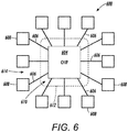
FIG. 6 illustrates a top view of the embedded electronic circuit component having electrical traces extending out to external pads or components, illustrating the more rigid substrate range and flexible substrate range as discussed in connection withFIGS. 4 and5 ; -
FIG. 7 illustrates an embodiment of a process according to the present application wherein a shaped tacky material is used to form a ramp for making electrical connections; -
FIG. 8 illustrates a side view of a printed interconnect to integrated circuits; -
FIG. 9 shows a top view ofFIG. 8 ; and -
FIGS 10A and 10B illustrate a substrate and an electronic circuit component which may be used in connection with the present teachings.. - In the following discussion the use of the term "electronic circuit component(s)" is to be understood to include any of a number of electronic circuit configurations including but not limited to bare die, electronic packaged electronic chips, among others.
- In order to provide a manufacturing process for electronic circuit component integration on a flexible substrate, the present discussion discloses methods and structures to facilitate high resolution connection with a printing process. In certain ones of the embodiments, a surface of the electronic circuit component, which carries electronic elements including contact pads and other electronic circuitry, is at the same level as the substrate (e.g., a cured bonding material). This arrangement permits high resolution patterning to be readily performed to construct or lay down conductive traces or connections between the circuitry on the electronic circuit component and circuitry on the substrate.
- To meet the challenge of the complexity of packaging, certain embodiments employ a printing technology, such as one commonly referred to as inkjet type printing which offers capabilities to enable high density and low resistance interconnections. Others include but are not limited to aerosol printing and extrusion printing. With use of printing technology (e.g., inkjet type, 3D, etc.), standard wire bonding processes can be replaced when the interconnections are made of printed conductive (e.g., metal) lines on a flat, planar level area. Thus the material being printed is understood to be a printable conductive material.
- Turning to
FIG. 1 illustrated is anassembly process 100, represented by a series of schematic diagrams 102-108 to construct a hybrid electronics platform assembly (discussed in more detail in U.S. Serial No. [Attorney Dkt. No. 20150242US02], entitled "Bare Die Integrator With Printed Component On Flexible Substrate", by Ping Mei et al.). - As illustrated in diagram 102, providing a
substrate 102A (in some embodiments the substrate is a flexible substrate, such as a plastic substrate).Substrate 102A has afirst surface 102B and second surface 102C opposite the first surface. These surfaces define the height of thesubstrate 102A. Thefirst surface 102B may includeelectronic circuitry 102D, such as but not limited to conductive circuit tracings. Also, while shown in side view, it is understoodsubstrate 102A of course also has width and length dimensions. - A material removal device (e.g., laser) 102E forms an opening 102F (the opening 102F defined by the parallel downward facing arrow lines) within a pre-identified location of
substrate 102A. More particularly at least one location on thefirst surface 102B of thesubstrate 102A appropriate to form the opening through the substrate is identified. Thereafter, thematerial removal device 102E performs a material removal operation to create the opening 102F in thesubstrate 102A, where the opening 102F is positioned within length and width boundaries of thesubstrate 102A, and the opening extends through thefirst surface 102B and the second surface 102C. - The
material removal device 102E is in one embodiment a laser arrangement, while in another embodiment it is a physical contact cutting device. In further embodiments other devices capable of precisely removing material to form opening 102F may be used. It is also to be understood that multiple openings may be made in a single substrate, and the assembly process ofFIG. 1 may be repeated a plurality of times for that same substrate, such that multiple openings may be formed. - The opening identified by 102F is made to conform to the shape and dimensions of a particular electronic circuit component (e.g., a bare die) being incorporated. However, a certain amount of clearance (e.g., about 5 - 25 µm) is provided to ensure the electronic circuit component is capable of being received. The
electronic circuit component 304B is at least one of a bare die or pre-packaged electronic circuit. - In a next step shown by diagram 104, opening 102F is more clearly depicted. It is mentioned here that diagram 104 (and the other diagrams of
FIG. 1 ) is a modified side or cross-sectional view, and for ease of understanding substrate material in front ofelectronic circuit component 104B is not shown. However it is to be understood that as the location of theelectronic circuit component 104B is within the boundaries of thesubstrate 102A, there would be portions of the substrate in front of theelectronic circuit component 104B, which would obstruct the view of agap 104E, as well as the portions of theelectronic circuit component 104B. It is to also be appreciated the other diagrams ofFIG. 1 are also modified side or cross-sectional views. - In diagram 104 the
substrate 102A has been turned over such thatfirst surface 102B (with circuits/traces 102D) is now facing downward. Additionally, atacky layer 104A with a tacky upper surface (e.g. a polydimethyisiloxane (PDMS) material, elastomer polymer, etc.), is positioned over the opening 102F, and at least a portion of thefirst surface 102B ofsubstrate 102A. Theelectronic circuit component 104B with itsfront surface 104C facing downward is then placed in the opening 102F. It is mentionedfront surface 104C includes conductive circuit traces (including contact pads, etc.) 104G. Also, it is understood thetacky layer 104A holds elements together but does not permanently bond the elements. - The upper face of the
flat article 104A with thetacky surface 104A may be considered analignment area 104D where thefirst surface 102B ofsubstrate 102A and thefirst surface 104C of theelectronic circuit component 104B are aligned in a substantially planar or flat or level relationship due to theflat article 104A. - Also shown in diagram 104 is
gap 104E which exists between the end of opening 102F andelectronic circuit component 104B. Thegap 104E is preferred to not be overly large, but sufficient to not interfere with the placement of theelectronic circuit component 104B (e.g., about 5-25µm). - Turning to diagram 106 of
FIG. 1 , abonding material 106A is applied on and over the second surface (the backside) 106B of theelectronic circuit component 104B, and on and over at least some portions of the second surface 102C of thesubstrate 102A. This backside may be understood to be anon-alignment area 106C where the second surface 102C of thesubstrate 102A and thesecond surface 106B of theelectronic circuit component 104B are not aligned (e.g., substantively planar or flat or level to each other). In other words the height of theelectronic circuit component 104B is greater than the height of the substrate. - In one embodiment the
bonding material 106A is a UV curable polymer dispensed onto the backside of the arrangement, the bonding material acting to seal thegap 104E. A fixing or curing arrangement (which may include curing lamps, heaters and/or other appropriate components) 106D is provided to perform fixing or curing on the bonding material (e.g., UV curable polymer). After UV curing, the UV cured polymer provides a bonding structure for the assembly. Of course, other bonding materials known in the art may also be employed in place of the UV bonding material. - In diagram 108 of
FIG. 1 , the assembly has been turned over and the tacky layer (e.g., a PDMS pad) 104A is separated and removed, exposing a substantially flat or planar or level surface spanning from thefirst surface 102B, across the filled ingap 104C' (i.e., filled in with thebonding material 106A to form a flat or planar surface), and further across thefirst surface 104D. It is mentioned the selected tacky material includes the characteristics of holding the mentioned components, but when separated does not leave behind undesirable amounts of residue that would otherwise interfere with the additional assembly process. Also, as an optional step, a cleaning of the component and substrate surfaces could be undertaken following separation and removal. - Finally,
conductive traces 108A, extending between thefirst surface 102B ofsubstrate 102A and thefirst surface 104Delectronic circuit component 104B are formed. In one embodiment traces 108A are generated by use of an inkjet type printing device 108B (using a conductive fluid). In an alternative embodiment the traces may be formed by use of photolithography, which requires a flat or planar or level surface to form conductive traces. - Turning to
FIG. 2 , illustrated is an exemplary electronic circuit component such as abare die arrangement 200, which has 36 contact pads 202 (not all pads numbered) with the smallest pitch about 120 um and the spacing between the pads to the edge 204 of the bare die is about 60 um. In practice, it is difficult to construct a ramp that is needed to seal a side wall of the die without covering the contact pads of the chip. - In order to provide a manufacturing process for electronic circuit component integration (including bare die, packaged chips, etc.) on a flexible, substrate, the inventors have developed a method and structure to facilitate high resolution connection with appropriate printing processes without the need to employ laser cutting. In certain embodiments, disclosed are methods and structures where a surface of an electronic circuit component is at the same level as a substrate formed from a bonding material. Therefore, high resolution patterning can be readily performed to construct conductive connections between the electronic circuit component and a circuit on the substrate.
- Turning to
FIG. 3 , illustrated is a particular embodiment of aprocess 300 used to embed an electronic circuit component such that it has a substantially flat or planar and exposed surface for electrical connection to components distant from theelectronic circuit component 304A. Inprocess 300, diagram 302 illustrates that atacky layer 302A (which may be a PDMS material or other appropriate material) is provided. Thetacky layer 302 includes atop surface 302B which has a tacky material carried thereon and abottom surface 302C. - Then in diagram 304, an
electronic circuit component 304A is provided (having similar characteristics to 104B ofFIG. 1 ) and has a first or front surface orside 304B and a back or second side orsurface 304C. The front or first surface orside 304B carries electronicconductive elements 304D, including but not limited to circuit traces and contact pads. As can be seen in thepresent process 300, the first orfront side 304B is placed in contact with the (tacky)surface 302B oftacky layer 302A. This provides a non-permanent securing of theelectronic circuit component 304A, such that it does not allow a liquid chemical to leak into the area under 304A to coversurface 304B and does not allow movement during the remainder of the process. - Turning to diagram 306, with the
electronic circuit component 304A in a secured relationship to thetacky layer 302A, abonding material 306A is deposited over thetacky surface 302B such that thebonding material 306A has a thickness or height sufficient to substantially hold theelectronic circuit component 304A. As shown in diagram 306, the depositing of thebonding material 306A may in one embodiment be accomplished by depositingdevice 306B, which in various embodiments may be printing devices such as inkjet printers, aerosol printers, among others. It is also to be appreciated that other forms of depositing thebonding material 306A may be employed. It is also shown in diagram 306 that once thebonding material 306A has been deposited, it is fixed or cured by a fixing or curingdevice 306C. In certain embodiments, thebonding material 306A is a UV curable polymer, and thecuring device 306C may be a light and/or heat generating device such as known in the art. It is to be appreciated, however, that other bonding materials that may be fixed or cured, such as to permanently set the bonding material, may also be employed. - With continuing attention to diagram 306, it may be seen that the fixed or cured
bonding material 306A includes asurface 306B which is substantially planar or in-line with first or front surface orside 304C ofelectronic circuit component 304A. This is seen more easily in diagram 308. - After the
bonding material 306A has been fixed or cured,tacky layer 302A is removed by separating or pulling away thetacky portion 302B from the cured, fixedbonding material 306A and theelectronic circuit component 304A. It is known that a PDMS and other material allows for removal without damaging components to which it has been connected. If desired, a cleaning operation may also be undertaken. - Turning to diagram 308, the structure has now been rotated approximately 180° such that first or front surface or
side 304B ofelectronic circuit component 304A is facing toward the upper end of the page. As can be seen in diagram 308, theelectronic circuit component 304A is now embedded in a permanent manner in the cured or fixedbonding material 306A. At this point, adepositing device 308A, such as a printer (e.g., inkjet printer, acoustic printer, etc.) is used to printconductive traces 308B to make a connection between theelectronic circuit component 304A to point 308C distant from theelectronic circuit component 304A.Point 308C may in one embodiment be a contact pad for other electronic elements (e.g., similar to that shown inFIG. 1 ). The cured or fixedbonding material 306A may be considered a form of substrate, particularly a flexible substrate without a gap between thesubstrate 306A and theelectronic component 304A. Also, as can be seen in diagram 308, theupper surface 306B of the fixed or curedbonding material 306A andsurface 304B are substantially in-line, even or planar with each other. This allows for the printer to simply print across this area for printing of the conductive traces without employing a ramp, and without employing cutting of a substrate such as done in the process ofFIG. 1 . - Turning to
FIG. 4 , illustrated is another embodiment of anassembly process 400 according to the present teachings. Diagram 402 illustrates that the process includes providing atacky layer 402A (e.g., a PDMS material or other appropriate layer) which has a tackyupper surface 402B and abottom surface 402C. In this embodiment and similar to that of diagram 304 (ofFIG. 3 ), diagram 404 of the present embodiment illustrates that anelectronic circuit component 404A (similar toelectronic circuit component 304A ofFIG. 3 ) is placed into contact with theupper surface 402B oftacky layer 402A, in such a way that a first or front surface orside 404B ofelectronic circuit component 404A is held by thetacky layer 402A, while the second or back side orsurface 404C of theelectronic circuit component 404A is not in contact with thetacky layer 402A. It is noted the front or first surface orside 404B contains electronic 404D elements such as but not limited to conductive tracings (including contact pads). - However, distinct from the previous embodiment, a
preliminary bonding material 404F is deposited on thesurface 402B of thetacky layer 402A and extending in a height dimension onto side walls 404G of theelectronic circuit component 404A. In one embodiment, thispreliminary bonding material 404F is deposited by adepositing device 404H, such as is known in the art, and would include but is not limited to inkjet type printers, aerosol printers, extrusion printing devices, etc. Once thepreliminary bonding material 404F has been deposited such that it extends up the side walls 404G (at least partially) ofelectronic circuit component 404A, a fixing or curing device 404I acts upon thebonding material 404F in order to fix or cure the preliminary bonding material to a permanent state. It is noted in one embodiment, thepreliminary bonding material 404F may be a UV curable polymer, and the curing or fixing device 404I may be a light/heat generating device sufficient to fix or cure the preliminary bonding material, as is known in the art. - Turning to diagram 406, once the
preliminary bonding material 404F has been fixed or cured, a second planarization orother bonding material 406A is deposited via adepositing device 406B. This may in certain embodiments be the same depositing device as used in diagram 404, while in other embodiments it may be different. Thebonding material 406A in certain embodiments is deposited to a thickness sufficient to cover theelectronic circuit component 404A as well as the preliminary fixedbonding material 404F. Following the depositing of thebonding material 406A, a fixing or curingdevice 406C ensures that the planarization or other bonding material is fixed or cured to a permanent state with asurface 406D (it is to be noted that the fixing or curingdevice 406C of diagram 406 may be a separate device from the curing or fixingdevice 404H of diagram 404, while in other embodiments, they may be the same device). - Following the fixing or curing of planarization or
other bonding material 406A,tacky layer 402A is removed in a manner such as known in the art and as previously discussed. - Thereafter, and as shown more clearly in diagram 408, the assembly is rotated essentially 180° in the drawing such that the surface of the
electronic circuit component 404A having conductive traces, contact pads, etc. 404D are shown pointing toward the top of drawing page. As can be seen in diagram 408,surface 404B ofelectronic circuit component 404A,surface 404J of thepreliminary bonding material 404F, andsurface 406D of the planarization orother bonding material 406A are substantially in-line, even or planar to each other with no gaps. This permits adepositing device 408A to printconductive traces 408B which extend off of theelectronic circuit component 404A across thepreliminary bonding material 404F and theplanarization bonding material 406A in a substantially planar manner. - In at least one embodiment, the
preliminary bonding material 404F is of a composition that is more rigid (less flexible) than the chemical composition of theplanarization bonding layer 406A. This aspect allows for the formation of a more rigid structure closer (e.g., 404F) to theelectronic circuit component 404A, while the remaining portion (e.g., 406A) of the substrate. The fixedpreliminary bonding material 404F (more rigid) and the planarization orother bonding material 406A (less rigid) may be considered a substrate on which electronic components may be provided and/or lead to other electronic devices (e.g., electronic chips, such as shown inFIG. 6 )). - Turning to
FIG. 5 , depicted is aprocess 500, including diagrams 502, 504, 506 and 508, which illustrate the formation of an embedded electronic circuit component (e.g., chip) with a substrate whose rigidity is a gradient from more rigid to less rigid (more flexible) as the distance from the electronic circuit component increases. Similar to the previous embodiments, diagram 502 shows atacky layer 502A having a front orfirst side 502B which carries a tacky material and a second surface 502C. Diagram 504, similar to the previous embodiments shows anelectronic circuit component 504A, having a front orfirst side surface 504B and a back or second side orsurface 504C. On the top orfront surface 504B areelectronic elements 504D (e.g., including but not limited to conductive traces and contact pads) 504D. Theelectronic circuit component 504A is in physical contact with the tacky front orfirst surface 502B oftacky layer 502A. This maintains theelectronic circuit component 504A in a secured (but not permanently fixed) position. This arrangement does not allow a liquid chemical to leak into the area under 504A and does not allow movement during the remainder of the process. - Turning to diagram 506, a
depositing device 506A is shown to include at least two separate depositing elements (e.g., print heads) 506B and 506C, to deposit a planarizationbonding material layer 506D. Thedepositing device 506A, which may be any of a number of known printing devices or extrusion devices, as previously discussed. In one embodiment, depositingelement 506B is supplied with a firstbonding material composition 506B', and depositingelement 506C is supplied with a secondbonding material composition 506C'. The firstbonding material composition 506B' is designed to be more rigid than the second bonding composition. - The
depositing device 506A is controlled to deposit the morerigid bonding composition 506B' nearer theelectronic circuit component 504A, and the secondbonding material composition 506C' more distant. It is understood that in certain embodiments the depositingelements second bonding compositions 506B', 506C' are mixed at locations in predetermined percentages to create a smooth gradient from rigid to less rigid, as the depositing moves more distant from theelectronic circuit component 504A as shown inFIG. 5 . - Thus, the
area 506E represents a more rigid non-flexible bonding material composition, where thearea 506F is a more flexible bonding material composition. Once deposited a fixing or curing device 506G is operated to fix or cure the compositions for a permanent holding of theelectronic circuit component 504A. Once thebonding material layer 506D has been fixed, thetacky layer 502A is removed using known techniques. - As shown in diagram 508 the assembly has been rotated 180° such that the upper or
first surface 504B is now pointing toward the upper end of the page, which results in the upper orfirst side 508A of thebonding material 506D to be substantially in-line or planar to the first orupper side 504B of theelectronic circuit component 504A. This, as in the previous embodiments, allows a depositing device (e.g., a printer) 508A to printconductive traces 508B across the electronicconductive component 504A and the fixed or curedbonding material layer 506D, which now acts as a substrate for theelectronic circuit component 504A. - Thus, similar to the process of
FIG. 4 , inFIG. 5 , the resulting substrate structure (e.g., the fixed or curedbonding material layer 506D) of diagram 508 is more rigid the closer to theelectronic circuit component 504A, and the more flexible (i.e., fixed or cured bonding material) the more distant from theelectronic circuit component 504A. A distinction between the two embodiments ofFIGS. 4 and5 is that while the process ofFIG. 4 requires two separate fixing or curing operations, the embodiment ofFIG. 5 provides for a single fixing or curing operation. - It is understood that in the
depositing device 506A shown in diagram 506, two depositingelements depositing device 506A may be computer controlled to first deposit the bonding material (more rigid material) near theelectronic circuit component 504A. Then as it moves forward, it is fed with a more flexible bonding composition. - Turning to
FIG. 6 , illustrated is atop view 600 of an arrangement employ the concepts ofFIGS. 4 and5 which have been discussed. More particularly, anelectronic circuit component 604 similar to the previously discussed electronic circuit components (404A and 504A) is shown with conductive traces 606 (not all traces are numbered), which extend out to contact pads and/orelectronic devices 608 that are on or past the described substrate (e.g., fixed or cured bonding material; e.g., 406A ofFIG. 4 , and 506A ofFIG. 5 ). As shown inFIG. 6 , anarea 610 , within a dashed line 612 (closer to the electronic circuit component 604) represents a more rigid substrate area than the material or area 612 extending past the dotted line 612 to theelectronic components 608. - The embodiments of
FIGS. 3 ,4 ,5 describe methods and arrangements where electrical conductive traces are laid down between electronic circuit components and distant connections (e.g., contact pads) in rampless designs. - Turning to
FIG. 7 , illustrated is another embodiment of aprocess 700 including diagrams 702, 704, 706 and 708. In diagram 702, atacky material 702A (e.g., PDMS) is designed with slopingside walls planar area 702D there between, creating acavity portion 703. Anelectronic circuit component 704A (similar to those previously discussed) includes a first or front side orsurface 704B and a second or back side orsurface 704C, where the front orfirst surface 704B includes conductive tracings (including contact pads) 704D, similar to those previously discussed. In diagram 702, theelectronic circuit component 704A is placed in contact with theplanar surface 702D, such that it is in a non-permanently fixed association. - In diagram 704, it is shown that a
bonding material 704F is deposited by depositingdevice 704G into the cutout area orcavity 703 formed by slopingwalls tacky material 702A. It is filled up to be substantially level with thetacky material 702A. Thereafter, in diagram 706, a flexibletransparent substrate 706A is positioned over the cutout area, and a curing or fixingcomponent 706B cures or fixes thebonding material 704F. - Thereafter, and similar to previous embodiments, the
tacky material 702A is removed, and as shown in diagram 708, the first orfront surface 704B of theelectronic component device 704A is in a fixed position wherein ramps 708A, 708B are provided. In this embodiment, aprinter 708C prints a conductive trace 708D extending between theelectronic circuit component 704A onto thesubstrate 706A. - Turning now to
FIGS. 8 and9 , it is known that combining hybrid electronic circuits to include electronic circuit components (e.g., packaged or bare die ICs) with printed electronics is a challenge due to the relative size differences between what can be achieved with printed conductive tracks and the small size and density of connection pads such as on Integrated Circuits (ICs). One must also solve the issue of how the IC is oriented to make the most reliable connection to the printed conductors. One way is to have the IC with the connection pads facing up. However, the printing method would have to be able to transition from the substrate surface level where the IC is placed to the ICs top surface where the connection pads are located. - The present embodiment of
FIGS. 8 and9 describe a method and arrangement which connects the IC pads to printed conductors on the substrate surface with the use of focused aerosol deposition device (e.g., from Optomec). The method uses accurate knowledge of the IC's location and geometry along with the location of the pads to connect in relation to a printed conductor trace with which a connection is to be made. - As illustrated in the side view of
FIG. 8 , the method andarrangement 800 shows a portion of an extrudedconductor 802 and a portion of an electronic circuit component (e.g., bare die, IC, etc.) 804 a certain known distance from each other on asubstrate 806. The process includes usingdeposition system 808, such as an aerosol deposition device for generating a printed trace (e.g., 20 to 40µm line width). Thesystem 808 is made to operate at a specific drawing speeds. Particularly as the conductive trace is being drawn from an edge of theelectronic circuit component 802, the printing speed is slowed down to deposit an increasinglytall trace 810 in order to match the height of theelectronic circuit component 804, when the deposited conductive material (i.e., in the form of trace 810) reaches the edge of the electronic circuit component 804B. From there the speed is increased to reduce theheight 812 of the conductive trace. Particularly, the height of thetrace 810 atlocation 812 is much less than the height of the trace prior to reaching thecomponent 804. The trace is continued until thecontact pad 814 is reached. - In one embodiment, an exact electronic circuit component location placed on a substrate is determined through calibrated
machine vision element 816, and the electronic circuit component step height obtained in combination with an optical profiler element 818 (for example, by a Precitec confocal instrument from Precitec Group). - Turning now to
FIGS. 10A and 10B . In the foregoing embodiments, the respective electronic circuitry is substantially level or planar with a surface of the respective substrates. However, it is to be understood the present concepts are also applicable when the electronic circuitry and substrates are not level. For example, inFIGS. 10A and 10B , illustrated is asubstrate 1000 and anelectronic circuit component 1002. As can be seen, the electronic circuitry or traces 1000A onsubstrate 1000, and electronic circuity or traces 1002A onelectronic component 1002, rise in profile above therespective surfaces electronic circuity component 1002 is placed in contact with a material (for example, PDMS) which is sufficiently soft, this allowselements 1002A to push into the PDMS material providing an appropriate positioning arrangement for the remainder of the process to be undertaken. - Also, when a conductive trace is formed between
substrate 1000 andcomponent 1002, there is sufficient depositing height to generate a substantially flat conductive line such as shown in the preceding figures. - The foregoing figures and discussions are noted to show embodiments for the fabrication of hybrid electronic platforms.
- The preceding discussion has described a method of forming an electronic assembly including the steps of providing a tacky layer. Providing an electronic circuit component having a first side and a second side, the first side carrying electronics. Positioning the first side of the electronic circuit component into contact with the tacky layer. Depositing a bonding material to a portion of the tacky layer not covered by the first side of the electronic circuit component to depth which substantially covers the second side of the electronic circuit component. Curing the bonding material into a cured bonding material. Finally, removing the tacky layer, wherein the electronic circuit component is held in secure attachment by the cured bonding material.
- Aspects of the described method are set forth below.
- The first surface of the electronic circuit component and a first surface of the cured bonding material are substantially planar to each other.
- Conductive traces are laid down between the cured bonding material and the first surface of the electronic circuit component.
- A preliminary bonding material is deposited prior to the step of depositing the bonding material. The preliminary bonding material extends along a portion of the tacky layer and up in a height direction along sides of the electronic circuit component. Then the preliminary bonding material is cured into a preliminary cured bonding material prior to the step of depositing the bonding material. The preliminary cured bonding material has a stiffer constitution than the cured bonding material.
- The deposited curable material consists of a stiffer material composition closer to the electronic circuit component and a less stiff material composition farther away from the electronic circuit component.
- The deposited curable material consists of (i) a stiffer material composition and (ii) a less stiff material composition are cured at substantially the same time during a same curing operation.
- The depositing is accomplished using at least two different print heads, containing different curable material compositions.
- The depositing is accomplished using a single print head with a varying UV curable polymer material.
- The tacky layer is formed with a cavity portion defined by sloping sides and a planar portion between the sloping sides, the planar portion being sized to receive the electronic circuit component. The positioning of the first side of the electronic circuit component in contact with the tacky layer is on a surface of the planar portion, wherein the first surface is in contact with a surface of the planar portion of the tacky layer. The depositing further including depositing the curable material to a portion of the tacky layer not covered by the first side of the electronic circuit component to a depth which substantially covers the backside of the electronic circuit component, substantially filing in the remaining cavity portion with the bonding material.
- A substantially transparent substrate on the surface of the tacky layer and a surface of the bonding material. The curing of the bonding material includes providing curing through the transparent substrate to the bonding material to cure the bonding material. The removing of the tacky layer provides a ramp configuration on each side of the conductive electronic component.
- The depositing of the bonding material is at least one of ink-jet type printing, aerosol type printing, and extrusion type printing.
- The described steps form an electronic chip which includes an electronic circuit component having electronic elements on a first surface; a cured bonding material having a depth sufficient to substantially cover the second surface of the electronic circuit component, wherein the electronic circuit component is held in a secured relationship by the cured bonding material; an upper surface composed of the first surface of the electronic circuit component and at least a portion of the cured bonding material; and printed conductive traces extending between the cured bonding material and the first surface of the electronic circuit component.
- The assembly being designed where the cured bonding material consists of more than a single bonding material composition, wherein a bonding material composition closer to the electronic circuit component has a stiffer composition than another bonding material composition farther from the electronic circuit component.
- The first surface of the electronic circuit component and a first surface the cured bonding material are substantially planar with respect to each other.
- The cured bonding material is formed in a ramp configuration on each side of the conductive electronic component.
- The depositing of the bonding material is at least one of ink-jet type printing, aerosol type printing, and extrusion type printing.
- In another embodiment disclosed is a method of forming an electronic assembly including, providing a conductor on a substrate; providing an electronic circuit component on the substrate distanced from the conductor, wherein a height of the conductor is less than a height of the electronic circuit conductor; and determining the difference in height and distance between the conductor and the electronic circuit component operating an aerosol printing device to change speeds of depositing dependent upon the determined difference between the conductors and the electronic circuit component, and thereby alter the amount of material aerosol printer is laying down at a particular area.
- The method above, further includes slowing the aerosol printer down as it nears the electronic circuit component, thereby increasing the depth of the material until the material depth is equal to or above the height of the electronic circuit component, and speeding up the movement of the aerosol printer thereafter.
- It will be appreciated that variants of the above-disclosed and other features and functions, or alternatives thereof, may be combined into many other different systems or applications. Various presently unforeseen or unanticipated alternatives, modifications, variations or improvements therein may be subsequently made by those skilled in the art which are also intended to be encompassed by the following claims.
Claims (10)
- A method of forming an electronic assembly comprising:providing a tacky layerproviding an electronic circuit component having a first side and a second side, the first side carrying electronics;positioning the first side of the electronic circuit component into contact with the tacky layer;depositing a bonding material to a portion of the tacky layer not covered by the first side of the electronic circuit component to depth which substantially covers the second side of the electronic circuit component;curing the bonding material into a cured bonding materialremoving the tacky layer, wherein the electronic circuit component is held in secure attachment by the cured bonding material.
- The method according to claim 1 wherein the first surface of the electronic circuit component and a first surface of the cured bonding material are substantially planar to each other.
- The method of claim 2 further including laying down conductive traces between the cured bonding material and the first surface of the electronic circuit component.
- The method according to claim 1 further including:depositing a preliminary bonding material prior to the step of depositing the bonding material, wherein the preliminary bonding material extends along a portion of the tacky layer and up in a height direction along sides of the electronic circuit component; andcuring the preliminary bonding material into a preliminary cured bonding material prior to the step of depositing the bonding material, and wherein the preliminary cured bonding material has a stiffer constitution than the cured bonding material.
- The method according to claim 1 further including:forming the tacky layer with a cavity portion defined by sloping sides and a planar portion between the sloping sides, the planar portion being sized to receive the electronic circuit component;the positioning of the first side of the electronic circuit component in contact with the tacky layer is on a surface of the planar portion, wherein the first surface is in contact with a surface of the planar portion of the tacky layer; andthe depositing further including depositing the curable material to a portion of the tacky layer not covered by the first side of the electronic circuit component to a depth which substantially covers the backside of the electronic circuit component, substantially filing in the remaining cavity portion with the bonding material.
- The method according to claim 5 further including:positioning a substantially transparent substrate on the surface of the tacky layer and a surface of the bonding material;the curing of the bonding material includes providing curing through the transparent substrate to the bonding material to cure the bonding material; andthe removing of the tacky layer provides a ramp configuration on each side of the conductive electronic component.
- The method according to claim 1 wherein the depositing of the bonding material is at least one of ink-jet type printing, aerosol type printing, and extrusion type printing.
- An electronic chip assembly comprising:an electronic circuit component having electronic elements on a first surface;a cured bonding material having a depth sufficient to substantially cover the second (or backside) surface of the electronic circuit component, wherein the electronic circuit component is held in a secured relationship by the cured bonding material;an upper surface composed of the first surface of the electronic circuit component and at least a portion of the cured bonding material; andprinted conductive traces extending between the cured bonding material and the first surface of the electronic circuit component.
- A method of forming an electronic assembly comprising:providing a conductor on a substrate;providing an electronic circuit component on the substrate distanced from the conductor, wherein a height of the conductor is less than a height of the electronic circuit conductor;determining the difference in height and distance between the conductor and the electronic circuit component operating an aerosol printing device to change speeds of depositing dependent upon the determined difference between the conductors and the electronic circuit component, and thereby alter the amount of material aerosol printer is laying down at a particular area.
- The method according to claim 9, further including slowing the aerosol printer down as it nears the electronic circuit component, thereby increasing the depth of the material until the material depth is equal to or above the height of the electronic circuit component, and speeding up the movement of the aerosol printer thereafter.
Applications Claiming Priority (1)
| Application Number | Priority Date | Filing Date | Title |
|---|---|---|---|
| US14/965,039 US10165677B2 (en) | 2015-12-10 | 2015-12-10 | Bare die integration with printed components on flexible substrate without laser cut |
Publications (2)
| Publication Number | Publication Date |
|---|---|
| EP3188220A2 true EP3188220A2 (en) | 2017-07-05 |
| EP3188220A3 EP3188220A3 (en) | 2017-12-13 |
Family
ID=57681226
Family Applications (1)
| Application Number | Title | Priority Date | Filing Date |
|---|---|---|---|
| EP16202082.0A Withdrawn EP3188220A3 (en) | 2015-12-10 | 2016-12-02 | Bare die integration with printed components |
Country Status (3)
| Country | Link |
|---|---|
| US (2) | US10165677B2 (en) |
| EP (1) | EP3188220A3 (en) |
| JP (1) | JP6814030B2 (en) |
Families Citing this family (6)
| Publication number | Priority date | Publication date | Assignee | Title |
|---|---|---|---|---|
| US10206288B2 (en) * | 2015-08-13 | 2019-02-12 | Palo Alto Research Center Incorporated | Bare die integration with printed components on flexible substrate |
| US10847384B2 (en) | 2017-05-31 | 2020-11-24 | Palo Alto Research Center Incorporated | Method and fixture for chip attachment to physical objects |
| US10789522B2 (en) | 2018-12-07 | 2020-09-29 | Palo Alto Research Center Incorporated | Near-field communication device with antenna on elongated printed interconnect |
| US12456706B2 (en) * | 2019-08-26 | 2025-10-28 | X-Celeprint Limited | Variable stiffness modules |
| KR102817417B1 (en) | 2019-09-10 | 2025-06-11 | 삼성디스플레이 주식회사 | Display panel, display device havig the same and the manufacturing method of the display device |
| CN114953432A (en) * | 2022-05-20 | 2022-08-30 | 合肥本源量子计算科技有限责任公司 | Method for manufacturing signal transmission line by aerosol jet printing and application |
Family Cites Families (26)
| Publication number | Priority date | Publication date | Assignee | Title |
|---|---|---|---|---|
| FR2527036A1 (en) | 1982-05-14 | 1983-11-18 | Radiotechnique Compelec | METHOD FOR CONNECTING A SEMICONDUCTOR TO ELEMENTS OF A SUPPORT, PARTICULARLY A PORTABLE CARD |
| US4658330A (en) | 1985-09-09 | 1987-04-14 | Tektronix, Inc. | Mounting a hybrid circuit to a circuit board |
| EP1213755A3 (en) * | 1994-03-18 | 2005-05-25 | Hitachi Chemical Co., Ltd. | Fabrication process of semiconductor package and semiconductor package |
| US6815251B1 (en) | 1999-02-01 | 2004-11-09 | Micron Technology, Inc. | High density modularity for IC's |
| JP4649745B2 (en) | 2001-02-01 | 2011-03-16 | ソニー株式会社 | Light-emitting element transfer method |
| US6670698B1 (en) * | 2002-02-05 | 2003-12-30 | Amkor Technology, Inc. | Integrated circuit package mounting |
| US7208345B2 (en) | 2005-05-11 | 2007-04-24 | Infineon Technologies Ag | Method of manufacturing a semiconductor device comprising stacked chips and a corresponding semiconductor device |
| JP4538416B2 (en) * | 2006-02-03 | 2010-09-08 | 株式会社日立メディアエレクトロニクス | Optical pickup device, manufacturing method thereof, and optical drive device |
| US9681550B2 (en) | 2007-08-28 | 2017-06-13 | Joseph C. Fjelstad | Method of making a circuit subassembly |
| KR20100009896A (en) | 2008-07-21 | 2010-01-29 | 삼성전자주식회사 | Semiconductor device package and method of fabricating the same |
| WO2011128266A1 (en) * | 2010-04-12 | 2011-10-20 | Imec | Optical shear sensor and method of producing such an optical shear sensor |
| KR20120004777A (en) | 2010-07-07 | 2012-01-13 | 삼성전기주식회사 | Electronic component module and manufacturing method thereof |
| US8501544B2 (en) | 2010-08-31 | 2013-08-06 | Stats Chippac, Ltd. | Semiconductor device and method of forming adhesive material over semiconductor die and carrier to reduce die shifting during encapsulation |
| JP5552404B2 (en) * | 2010-09-14 | 2014-07-16 | 日東電工株式会社 | A heat-resistant adhesive tape for manufacturing a semiconductor device and a method for manufacturing a semiconductor device using the tape. |
| US20140291001A1 (en) | 2010-11-22 | 2014-10-02 | Bridge Semiconductor Corporation | Method of making hybrid wiring board with built-in stiffener and interposer and hybrid wiring board manufactured thereby |
| US20120268899A1 (en) | 2011-04-21 | 2012-10-25 | Tessera Research Llc | Reinforced fan-out wafer-level package |
| US8937382B2 (en) | 2011-06-27 | 2015-01-20 | Intel Corporation | Secondary device integration into coreless microelectronic device packages |
| US10388584B2 (en) | 2011-09-06 | 2019-08-20 | STATS ChipPAC Pte. Ltd. | Semiconductor device and method of forming Fo-WLCSP with recessed interconnect area in peripheral region of semiconductor die |
| EP2639278A1 (en) | 2012-03-13 | 2013-09-18 | Nitto Denko Corporation | Heat-resistant pressure-sensitive adhesive tape for production of semiconductor device and method for producing seminconductor device using the tape |
| JP5987696B2 (en) * | 2013-01-09 | 2016-09-07 | 富士通株式会社 | Manufacturing method of semiconductor device |
| US8975739B2 (en) * | 2013-01-11 | 2015-03-10 | Xintec Inc. | Package structure and method for manufacturing thereof |
| DE102013201926B4 (en) | 2013-02-06 | 2025-12-04 | Robert Bosch Gmbh | Methods for electrically contacting a component and component assembly |
| TWI518852B (en) | 2013-10-02 | 2016-01-21 | 矽品精密工業股份有限公司 | Semiconductor package and its manufacturing method |
| CN104701190A (en) * | 2013-12-06 | 2015-06-10 | 毅宝力科技有限公司 | Systems and methods for fabricating cavity-down fabrication carriers |
| US9396972B2 (en) | 2014-02-11 | 2016-07-19 | Palo Alto Research Center Incorporated | Micro-assembly with planarized embedded microelectronic dies |
| US10206288B2 (en) | 2015-08-13 | 2019-02-12 | Palo Alto Research Center Incorporated | Bare die integration with printed components on flexible substrate |
-
2015
- 2015-12-10 US US14/965,039 patent/US10165677B2/en active Active
-
2016
- 2016-11-22 JP JP2016227298A patent/JP6814030B2/en active Active
- 2016-12-02 EP EP16202082.0A patent/EP3188220A3/en not_active Withdrawn
-
2018
- 2018-11-14 US US16/190,324 patent/US11122683B2/en active Active
Non-Patent Citations (1)
| Title |
|---|
| None |
Also Published As
| Publication number | Publication date |
|---|---|
| JP2017108120A (en) | 2017-06-15 |
| US20190124757A1 (en) | 2019-04-25 |
| JP6814030B2 (en) | 2021-01-13 |
| EP3188220A3 (en) | 2017-12-13 |
| US20170171958A1 (en) | 2017-06-15 |
| US11122683B2 (en) | 2021-09-14 |
| US10165677B2 (en) | 2018-12-25 |
Similar Documents
| Publication | Publication Date | Title |
|---|---|---|
| US11122683B2 (en) | Bare die integration with printed components on flexible substrate without laser cut | |
| EP3131114B1 (en) | Bare die integration within a flexible substrate | |
| KR100872212B1 (en) | Liquid discharge head, and method of manufacturing liquid discharge head | |
| JP2010182137A (en) | Touch panel and method for manufacturing the same | |
| US8074350B2 (en) | Method of printing electronic circuits | |
| US20160152029A1 (en) | Ink-jet recording head, recording element substrate, method for manufacturing ink-jet recording head, and method for manufacturing recording element substrate | |
| EP3485511B1 (en) | Method of manufacturing flexible electronic circuits having conformal material coatings | |
| KR20190002503A (en) | Ceramic circuit board and manufacturing method thereof | |
| CA3134189A1 (en) | Foldable digital microfluidic (dmf) device using flexible electronic platform and methods of making same | |
| US20180160548A1 (en) | Patterned overcoat layer | |
| US10477699B2 (en) | Method for manufacturing electronic component attached wiring board | |
| JP2011199184A (en) | Substrate mounting device and substrate mounting method | |
| US10847384B2 (en) | Method and fixture for chip attachment to physical objects | |
| JP7540000B2 (en) | A barrier against floating SMT components | |
| CN107548573A (en) | Printed circuit board to mold compound junction | |
| KR20170022934A (en) | Squeegee printing on descended surfaces | |
| CN220258596U (en) | Display module assembly rubber coating stop device | |
| JP7739131B2 (en) | Liquid ejection head and manufacturing method thereof | |
| WO2021206732A1 (en) | Blocking fluid progression among layers of fluidic devices | |
| US12134274B2 (en) | Molded structures with channels | |
| JP2007180397A (en) | Printed wiring board and liquid crystal display device | |
| WO2021183134A1 (en) | Device with fluid directing trenches | |
| CN100511578C (en) | Die attach area cut-on-fly method and apparatus | |
| JP2005235849A (en) | Thin substrate fixture | |
| JP2003182027A (en) | Printing squeegee structure and printing apparatus |
Legal Events
| Date | Code | Title | Description |
|---|---|---|---|
| PUAI | Public reference made under article 153(3) epc to a published international application that has entered the european phase |
Free format text: ORIGINAL CODE: 0009012 |
|
| STAA | Information on the status of an ep patent application or granted ep patent |
Free format text: STATUS: THE APPLICATION HAS BEEN PUBLISHED |
|
| AK | Designated contracting states |
Kind code of ref document: A2 Designated state(s): AL AT BE BG CH CY CZ DE DK EE ES FI FR GB GR HR HU IE IS IT LI LT LU LV MC MK MT NL NO PL PT RO RS SE SI SK SM TR |
|
| AX | Request for extension of the european patent |
Extension state: BA ME |
|
| PUAL | Search report despatched |
Free format text: ORIGINAL CODE: 0009013 |
|
| AK | Designated contracting states |
Kind code of ref document: A3 Designated state(s): AL AT BE BG CH CY CZ DE DK EE ES FI FR GB GR HR HU IE IS IT LI LT LU LV MC MK MT NL NO PL PT RO RS SE SI SK SM TR |
|
| AX | Request for extension of the european patent |
Extension state: BA ME |
|
| RIC1 | Information provided on ipc code assigned before grant |
Ipc: H01L 21/56 20060101AFI20171103BHEP Ipc: H01L 23/31 20060101ALI20171103BHEP Ipc: H01L 23/48 20060101ALI20171103BHEP |
|
| STAA | Information on the status of an ep patent application or granted ep patent |
Free format text: STATUS: REQUEST FOR EXAMINATION WAS MADE |
|
| 17P | Request for examination filed |
Effective date: 20180613 |
|
| RBV | Designated contracting states (corrected) |
Designated state(s): AL AT BE BG CH CY CZ DE DK EE ES FI FR GB GR HR HU IE IS IT LI LT LU LV MC MK MT NL NO PL PT RO RS SE SI SK SM TR |
|
| STAA | Information on the status of an ep patent application or granted ep patent |
Free format text: STATUS: EXAMINATION IS IN PROGRESS |
|
| 17Q | First examination report despatched |
Effective date: 20210305 |
|
| STAA | Information on the status of an ep patent application or granted ep patent |
Free format text: STATUS: THE APPLICATION IS DEEMED TO BE WITHDRAWN |
|
| 18D | Application deemed to be withdrawn |
Effective date: 20250408 |