EP3187924A1 - Display device - Google Patents
Display device Download PDFInfo
- Publication number
- EP3187924A1 EP3187924A1 EP16205407.6A EP16205407A EP3187924A1 EP 3187924 A1 EP3187924 A1 EP 3187924A1 EP 16205407 A EP16205407 A EP 16205407A EP 3187924 A1 EP3187924 A1 EP 3187924A1
- Authority
- EP
- European Patent Office
- Prior art keywords
- pixel electrode
- main trunk
- substrate
- display device
- interlayer
- Prior art date
- Legal status (The legal status is an assumption and is not a legal conclusion. Google has not performed a legal analysis and makes no representation as to the accuracy of the status listed.)
- Granted
Links
Images


Classifications
-
- G—PHYSICS
- G02—OPTICS
- G02F—OPTICAL DEVICES OR ARRANGEMENTS FOR THE CONTROL OF LIGHT BY MODIFICATION OF THE OPTICAL PROPERTIES OF THE MEDIA OF THE ELEMENTS INVOLVED THEREIN; NON-LINEAR OPTICS; FREQUENCY-CHANGING OF LIGHT; OPTICAL LOGIC ELEMENTS; OPTICAL ANALOGUE/DIGITAL CONVERTERS
- G02F1/00—Devices or arrangements for the control of the intensity, colour, phase, polarisation or direction of light arriving from an independent light source, e.g. switching, gating or modulating; Non-linear optics
- G02F1/01—Devices or arrangements for the control of the intensity, colour, phase, polarisation or direction of light arriving from an independent light source, e.g. switching, gating or modulating; Non-linear optics for the control of the intensity, phase, polarisation or colour
- G02F1/13—Devices or arrangements for the control of the intensity, colour, phase, polarisation or direction of light arriving from an independent light source, e.g. switching, gating or modulating; Non-linear optics for the control of the intensity, phase, polarisation or colour based on liquid crystals, e.g. single liquid crystal display cells
- G02F1/133—Constructional arrangements; Operation of liquid crystal cells; Circuit arrangements
- G02F1/1333—Constructional arrangements; Manufacturing methods
- G02F1/1343—Electrodes
- G02F1/134309—Electrodes characterised by their geometrical arrangement
-
- G—PHYSICS
- G02—OPTICS
- G02F—OPTICAL DEVICES OR ARRANGEMENTS FOR THE CONTROL OF LIGHT BY MODIFICATION OF THE OPTICAL PROPERTIES OF THE MEDIA OF THE ELEMENTS INVOLVED THEREIN; NON-LINEAR OPTICS; FREQUENCY-CHANGING OF LIGHT; OPTICAL LOGIC ELEMENTS; OPTICAL ANALOGUE/DIGITAL CONVERTERS
- G02F1/00—Devices or arrangements for the control of the intensity, colour, phase, polarisation or direction of light arriving from an independent light source, e.g. switching, gating or modulating; Non-linear optics
- G02F1/01—Devices or arrangements for the control of the intensity, colour, phase, polarisation or direction of light arriving from an independent light source, e.g. switching, gating or modulating; Non-linear optics for the control of the intensity, phase, polarisation or colour
- G02F1/13—Devices or arrangements for the control of the intensity, colour, phase, polarisation or direction of light arriving from an independent light source, e.g. switching, gating or modulating; Non-linear optics for the control of the intensity, phase, polarisation or colour based on liquid crystals, e.g. single liquid crystal display cells
- G02F1/133—Constructional arrangements; Operation of liquid crystal cells; Circuit arrangements
- G02F1/1333—Constructional arrangements; Manufacturing methods
- G02F1/133371—Cells with varying thickness of the liquid crystal layer
-
- G—PHYSICS
- G02—OPTICS
- G02F—OPTICAL DEVICES OR ARRANGEMENTS FOR THE CONTROL OF LIGHT BY MODIFICATION OF THE OPTICAL PROPERTIES OF THE MEDIA OF THE ELEMENTS INVOLVED THEREIN; NON-LINEAR OPTICS; FREQUENCY-CHANGING OF LIGHT; OPTICAL LOGIC ELEMENTS; OPTICAL ANALOGUE/DIGITAL CONVERTERS
- G02F1/00—Devices or arrangements for the control of the intensity, colour, phase, polarisation or direction of light arriving from an independent light source, e.g. switching, gating or modulating; Non-linear optics
- G02F1/01—Devices or arrangements for the control of the intensity, colour, phase, polarisation or direction of light arriving from an independent light source, e.g. switching, gating or modulating; Non-linear optics for the control of the intensity, phase, polarisation or colour
- G02F1/13—Devices or arrangements for the control of the intensity, colour, phase, polarisation or direction of light arriving from an independent light source, e.g. switching, gating or modulating; Non-linear optics for the control of the intensity, phase, polarisation or colour based on liquid crystals, e.g. single liquid crystal display cells
- G02F1/133—Constructional arrangements; Operation of liquid crystal cells; Circuit arrangements
- G02F1/1333—Constructional arrangements; Manufacturing methods
- G02F1/133345—Insulating layers
-
- G—PHYSICS
- G02—OPTICS
- G02F—OPTICAL DEVICES OR ARRANGEMENTS FOR THE CONTROL OF LIGHT BY MODIFICATION OF THE OPTICAL PROPERTIES OF THE MEDIA OF THE ELEMENTS INVOLVED THEREIN; NON-LINEAR OPTICS; FREQUENCY-CHANGING OF LIGHT; OPTICAL LOGIC ELEMENTS; OPTICAL ANALOGUE/DIGITAL CONVERTERS
- G02F1/00—Devices or arrangements for the control of the intensity, colour, phase, polarisation or direction of light arriving from an independent light source, e.g. switching, gating or modulating; Non-linear optics
- G02F1/01—Devices or arrangements for the control of the intensity, colour, phase, polarisation or direction of light arriving from an independent light source, e.g. switching, gating or modulating; Non-linear optics for the control of the intensity, phase, polarisation or colour
- G02F1/13—Devices or arrangements for the control of the intensity, colour, phase, polarisation or direction of light arriving from an independent light source, e.g. switching, gating or modulating; Non-linear optics for the control of the intensity, phase, polarisation or colour based on liquid crystals, e.g. single liquid crystal display cells
- G02F1/133—Constructional arrangements; Operation of liquid crystal cells; Circuit arrangements
- G02F1/1333—Constructional arrangements; Manufacturing methods
- G02F1/1337—Surface-induced orientation of the liquid crystal molecules, e.g. by alignment layers
- G02F1/133707—Structures for producing distorted electric fields, e.g. bumps, protrusions, recesses, slits in pixel electrodes
-
- G—PHYSICS
- G02—OPTICS
- G02F—OPTICAL DEVICES OR ARRANGEMENTS FOR THE CONTROL OF LIGHT BY MODIFICATION OF THE OPTICAL PROPERTIES OF THE MEDIA OF THE ELEMENTS INVOLVED THEREIN; NON-LINEAR OPTICS; FREQUENCY-CHANGING OF LIGHT; OPTICAL LOGIC ELEMENTS; OPTICAL ANALOGUE/DIGITAL CONVERTERS
- G02F1/00—Devices or arrangements for the control of the intensity, colour, phase, polarisation or direction of light arriving from an independent light source, e.g. switching, gating or modulating; Non-linear optics
- G02F1/01—Devices or arrangements for the control of the intensity, colour, phase, polarisation or direction of light arriving from an independent light source, e.g. switching, gating or modulating; Non-linear optics for the control of the intensity, phase, polarisation or colour
- G02F1/13—Devices or arrangements for the control of the intensity, colour, phase, polarisation or direction of light arriving from an independent light source, e.g. switching, gating or modulating; Non-linear optics for the control of the intensity, phase, polarisation or colour based on liquid crystals, e.g. single liquid crystal display cells
- G02F1/133—Constructional arrangements; Operation of liquid crystal cells; Circuit arrangements
- G02F1/1333—Constructional arrangements; Manufacturing methods
- G02F1/1343—Electrodes
- G02F1/13439—Electrodes characterised by their electrical, optical, physical properties; materials therefor; method of making
-
- G—PHYSICS
- G02—OPTICS
- G02F—OPTICAL DEVICES OR ARRANGEMENTS FOR THE CONTROL OF LIGHT BY MODIFICATION OF THE OPTICAL PROPERTIES OF THE MEDIA OF THE ELEMENTS INVOLVED THEREIN; NON-LINEAR OPTICS; FREQUENCY-CHANGING OF LIGHT; OPTICAL LOGIC ELEMENTS; OPTICAL ANALOGUE/DIGITAL CONVERTERS
- G02F1/00—Devices or arrangements for the control of the intensity, colour, phase, polarisation or direction of light arriving from an independent light source, e.g. switching, gating or modulating; Non-linear optics
- G02F1/01—Devices or arrangements for the control of the intensity, colour, phase, polarisation or direction of light arriving from an independent light source, e.g. switching, gating or modulating; Non-linear optics for the control of the intensity, phase, polarisation or colour
- G02F1/13—Devices or arrangements for the control of the intensity, colour, phase, polarisation or direction of light arriving from an independent light source, e.g. switching, gating or modulating; Non-linear optics for the control of the intensity, phase, polarisation or colour based on liquid crystals, e.g. single liquid crystal display cells
- G02F1/133—Constructional arrangements; Operation of liquid crystal cells; Circuit arrangements
- G02F1/136—Liquid crystal cells structurally associated with a semi-conducting layer or substrate, e.g. cells forming part of an integrated circuit
- G02F1/1362—Active matrix addressed cells
- G02F1/136286—Wiring, e.g. gate line, drain line
-
- G—PHYSICS
- G02—OPTICS
- G02F—OPTICAL DEVICES OR ARRANGEMENTS FOR THE CONTROL OF LIGHT BY MODIFICATION OF THE OPTICAL PROPERTIES OF THE MEDIA OF THE ELEMENTS INVOLVED THEREIN; NON-LINEAR OPTICS; FREQUENCY-CHANGING OF LIGHT; OPTICAL LOGIC ELEMENTS; OPTICAL ANALOGUE/DIGITAL CONVERTERS
- G02F1/00—Devices or arrangements for the control of the intensity, colour, phase, polarisation or direction of light arriving from an independent light source, e.g. switching, gating or modulating; Non-linear optics
- G02F1/01—Devices or arrangements for the control of the intensity, colour, phase, polarisation or direction of light arriving from an independent light source, e.g. switching, gating or modulating; Non-linear optics for the control of the intensity, phase, polarisation or colour
- G02F1/13—Devices or arrangements for the control of the intensity, colour, phase, polarisation or direction of light arriving from an independent light source, e.g. switching, gating or modulating; Non-linear optics for the control of the intensity, phase, polarisation or colour based on liquid crystals, e.g. single liquid crystal display cells
- G02F1/133—Constructional arrangements; Operation of liquid crystal cells; Circuit arrangements
- G02F1/1333—Constructional arrangements; Manufacturing methods
- G02F1/1343—Electrodes
-
- G—PHYSICS
- G02—OPTICS
- G02F—OPTICAL DEVICES OR ARRANGEMENTS FOR THE CONTROL OF LIGHT BY MODIFICATION OF THE OPTICAL PROPERTIES OF THE MEDIA OF THE ELEMENTS INVOLVED THEREIN; NON-LINEAR OPTICS; FREQUENCY-CHANGING OF LIGHT; OPTICAL LOGIC ELEMENTS; OPTICAL ANALOGUE/DIGITAL CONVERTERS
- G02F1/00—Devices or arrangements for the control of the intensity, colour, phase, polarisation or direction of light arriving from an independent light source, e.g. switching, gating or modulating; Non-linear optics
- G02F1/01—Devices or arrangements for the control of the intensity, colour, phase, polarisation or direction of light arriving from an independent light source, e.g. switching, gating or modulating; Non-linear optics for the control of the intensity, phase, polarisation or colour
- G02F1/13—Devices or arrangements for the control of the intensity, colour, phase, polarisation or direction of light arriving from an independent light source, e.g. switching, gating or modulating; Non-linear optics for the control of the intensity, phase, polarisation or colour based on liquid crystals, e.g. single liquid crystal display cells
- G02F1/133—Constructional arrangements; Operation of liquid crystal cells; Circuit arrangements
- G02F1/1333—Constructional arrangements; Manufacturing methods
- G02F1/1343—Electrodes
- G02F1/134309—Electrodes characterised by their geometrical arrangement
- G02F1/134345—Subdivided pixels, e.g. for grey scale or redundancy
-
- G—PHYSICS
- G02—OPTICS
- G02F—OPTICAL DEVICES OR ARRANGEMENTS FOR THE CONTROL OF LIGHT BY MODIFICATION OF THE OPTICAL PROPERTIES OF THE MEDIA OF THE ELEMENTS INVOLVED THEREIN; NON-LINEAR OPTICS; FREQUENCY-CHANGING OF LIGHT; OPTICAL LOGIC ELEMENTS; OPTICAL ANALOGUE/DIGITAL CONVERTERS
- G02F1/00—Devices or arrangements for the control of the intensity, colour, phase, polarisation or direction of light arriving from an independent light source, e.g. switching, gating or modulating; Non-linear optics
- G02F1/01—Devices or arrangements for the control of the intensity, colour, phase, polarisation or direction of light arriving from an independent light source, e.g. switching, gating or modulating; Non-linear optics for the control of the intensity, phase, polarisation or colour
- G02F1/13—Devices or arrangements for the control of the intensity, colour, phase, polarisation or direction of light arriving from an independent light source, e.g. switching, gating or modulating; Non-linear optics for the control of the intensity, phase, polarisation or colour based on liquid crystals, e.g. single liquid crystal display cells
- G02F1/137—Devices or arrangements for the control of the intensity, colour, phase, polarisation or direction of light arriving from an independent light source, e.g. switching, gating or modulating; Non-linear optics for the control of the intensity, phase, polarisation or colour based on liquid crystals, e.g. single liquid crystal display cells characterised by the electro-optical or magneto-optical effect, e.g. field-induced phase transition, orientation effect, guest-host interaction or dynamic scattering
-
- G—PHYSICS
- G02—OPTICS
- G02F—OPTICAL DEVICES OR ARRANGEMENTS FOR THE CONTROL OF LIGHT BY MODIFICATION OF THE OPTICAL PROPERTIES OF THE MEDIA OF THE ELEMENTS INVOLVED THEREIN; NON-LINEAR OPTICS; FREQUENCY-CHANGING OF LIGHT; OPTICAL LOGIC ELEMENTS; OPTICAL ANALOGUE/DIGITAL CONVERTERS
- G02F2201/00—Constructional arrangements not provided for in groups G02F1/00 - G02F7/00
- G02F2201/12—Constructional arrangements not provided for in groups G02F1/00 - G02F7/00 electrode
- G02F2201/121—Constructional arrangements not provided for in groups G02F1/00 - G02F7/00 electrode common or background
-
- G—PHYSICS
- G02—OPTICS
- G02F—OPTICAL DEVICES OR ARRANGEMENTS FOR THE CONTROL OF LIGHT BY MODIFICATION OF THE OPTICAL PROPERTIES OF THE MEDIA OF THE ELEMENTS INVOLVED THEREIN; NON-LINEAR OPTICS; FREQUENCY-CHANGING OF LIGHT; OPTICAL LOGIC ELEMENTS; OPTICAL ANALOGUE/DIGITAL CONVERTERS
- G02F2201/00—Constructional arrangements not provided for in groups G02F1/00 - G02F7/00
- G02F2201/12—Constructional arrangements not provided for in groups G02F1/00 - G02F7/00 electrode
- G02F2201/123—Constructional arrangements not provided for in groups G02F1/00 - G02F7/00 electrode pixel
-
- G—PHYSICS
- G02—OPTICS
- G02F—OPTICAL DEVICES OR ARRANGEMENTS FOR THE CONTROL OF LIGHT BY MODIFICATION OF THE OPTICAL PROPERTIES OF THE MEDIA OF THE ELEMENTS INVOLVED THEREIN; NON-LINEAR OPTICS; FREQUENCY-CHANGING OF LIGHT; OPTICAL LOGIC ELEMENTS; OPTICAL ANALOGUE/DIGITAL CONVERTERS
- G02F2201/00—Constructional arrangements not provided for in groups G02F1/00 - G02F7/00
- G02F2201/40—Arrangements for improving the aperture ratio
Definitions
- the disclosure relates to a display device.
- the liquid crystal display device To develop its functions towards high contrast ratio, no gray scale inversion, low color shift, high luminance, full color, high color saturation, high response speed, and a wide viewing angle.
- the technologies capable of meeting the requirement of a wide viewing angle include the twist nematic (TN) liquid crystal having a wide viewing film, the in-plane switching (IPS) liquid crystal display device, the fringe field switching liquid crystal display device, and the multi-domain vertical alignment (MVA) liquid crystal display device.
- TN twist nematic
- IPS in-plane switching
- MVA multi-domain vertical alignment
- the technology of Low color shift is developed for solving this problem, different voltages separately provided to two separate pixel electrodes in a the sub-pixel area, at least one more transistor is need to control the pixel electrodes, as a result, a tilt degree of liquid crystal molecules driven by the separate pixel electrodes are also different to mitigate the issues of color shift and insufficient color saturation.
- such design increases a number of the thin film transistors and meanwhile increases a number of the scan lines. It not only increases a probability of lowering the process yield rate, but also lowers the aperture rate of the liquid crystal display device.
- the disclosure provides a display device capable of solving issues of a low process yield rate or a low aperture ratio in the current wide viewing angle technology.
- the display device includes a first substrate, at least two scan lines, at least two data lines, at least a pixel electrode, at least an active component, a first interlayer, a second substrate, a common electrode layer, and a display medium layer.
- the scan lines, the data lines, the pixel electrode, and the active component are disposed over the first substrate. Adjacent two of the scan lines and adjacent two of the data lines intersect to define a sub-pixel area.
- the active component is electrically connected to one of the scan lines.
- the pixel electrode is electrically connected to the active component.
- the pixel electrode includes a first pixel electrode and a second pixel electrode having the same electric potential.
- the first interlayer is formed between the first substrate and the first pixel electrode of the pixel electrode.
- the first interlayer includes a plurality of first strip-shaped branches. Adjacent two of the first strip-shaped branches form a first gap to expose part of the first substrate.
- the common electrode layer is disposed over the second substrate.
- the display medium layer is disposed between the first substrate and the second substrate.
- the pixel electrode is positioned between the first substrate and the display medium layer.
- the first pixel electrode extends to cover the first gap.
- a maximum vertical distance between the first pixel electrode and the common electrode layer is a first distance.
- a maximum vertical distance between the second pixel electrode and the common electrode layer is a second distance.
- a difference between the first distance and the second distance is 0.1 ⁇ m to 0.4 ⁇ m.
- the second pixel electrode includes a plurality of second strip-shaped branches, wherein adjacent two of the strip-shaped branches form a second gap.
- the display device further includes a second interlayer disposed between the first substrate and the second pixel electrode.
- the second gap exposes part of the second interlayer.
- a material of at least one of the first interlayer and the second interlayer is identical to a material of the pixel electrode.
- the material of at least one of the first interlayer and the second interlayer is an insulating material.
- the first interlayer further includes a first main trunk and a second main trunk, the first main trunk and the second main trunk intersects.
- Each of the first strip-shaped branches connects to one of the first main trunk and the second main trunk.
- An included angle between one of the first strip-shaped branches and one of the first main trunk and the second main trunk is between 25° and 65°.
- the second pixel electrode includes a third main trunk and a fourth main trunk.
- the third main trunk and the fourth main trunk intersects.
- Each of the second strip-shaped branches connects to one of the third main trunk and the fourth main trunk.
- An included angle between one of the second strip-shaped branches and one of the third main trunk and the fourth main trunk is between 25° and 65°.
- the first pixel electrode directly connects to the second pixel electrode.
- the first interlayer comprises a sidewall and a bottom surface connected to the sidewall.
- An included angle between the sidewall and the bottom surface is between 40° and 90°.
- the display device includes a first substrate, at least two scan lines, at least two data lines, at least a pixel electrode, at least an active component, a first interlayer, a second substrate, a common electrode layer, and a display medium layer.
- the scan lines, the data lines, the pixel electrode, and the active component are disposed over the first substrate. Adjacent two of the scan lines and adjacent two of the data lines intersect to define a sub-pixel area.
- the active component is electrically connected to one of the scan line.
- the pixel electrode is electrically connected to the active component.
- the pixel electrode includes a first pixel electrode and a second pixel electrode having the same electric potential.
- the first interlayer is formed between the first substrate and the first pixel electrode of the pixel electrode.
- the first interlayer includes a plurality of first strip-shaped branches. Adjacent two of the first strip-shaped branches form a first gap to expose part of the first substrate.
- the common electrode layer is disposed over the second substrate.
- the display medium layer is disposed between the first substrate and the second substrate.
- the pixel electrode is positioned between the first substrate and the display medium layer. The first pixel electrode extends to cover the first gap.
- the second pixel electrode includes a plurality of second strip-shaped branches. Adjacent two of the second strip-shaped branches form a second gap. A minimum distance between the first pixel electrode and the common electrode layer is a third distance. A minimum distance between the second pixel electrode and the common electrode layer is a fourth distance. The third distance is different from the fourth distance.
- a difference between the third distance and the fourth distance is 0.1 ⁇ m to 0.4 ⁇ m.
- the second gap is between 3 ⁇ m and 10 ⁇ m.
- a thickness of the first interlayer is between 0.1 ⁇ m and 0.4 ⁇ m.
- the first interlayer includes a sidewall and a bottom surface connected to the sidewall.
- An included angle formed between the sidewall and the bottom surface is between 40° and 90°.
- the first interlayer further includes a first main trunk and a second main trunk.
- the first main trunk and the second main trunk intersects.
- Each of the first strip-shaped branches connects to one of the first main trunk and the second main trunk.
- An included angle between one of the first strip-shaped branches and one of the first main trunk and the second main trunk is between 25° and 65°.
- the second pixel electrode includes a third main trunk and a fourth main trunk.
- the third main trunk and the fourth main trunk intersects.
- Each of the second strip-shaped branches connects to one of the third main trunk and the fourth main trunk.
- An included angle between one of the second strip-shaped branches and one of the third main trunk and the fourth main trunk is between 25° and 65°.
- the first pixel electrode directly connects to the second pixel electrode.
- the pixel electrode (include first pixel electrode and second pixel electrode) of the display device of the disclosure has substantially the same electric potential.
- the distance between the first pixel electrode of the pixel electrode and the common electrode layer is different from the distance between the second pixel electrode of the pixel electrode and the common electrode layer. Accordingly, without increasing a number of the active component, brightness presented by the first pixel electrode and by the second pixel electrode can still be different to mitigate the issues of color shift and insufficient color saturation. Thereby, the process yield rate or the aperture ratio of the display device can be improved.
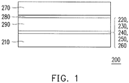
- FIG. 1 is a cross-sectional simplified schematic view of a display device according to one embodiment of the disclosure.
- FIG. 2 is a top view of a single sub-pixel area of the display device of FIG. 1 .
- a display device 200 according to one embodiment of the disclosure includes a first substrate 210, at least two scan lines 220, at least two data lines 230, at least a pixel electrode 240, at least an active component 250, a first interlayer 260, a second substrate 270, a common electrode layer 280, and a display medium layer 290.
- FIG. 2 only illustrates one single sub-pixel area. Upon referring to FIG.
- an arrangement of at least two or more scan lines 220, at least two or more data lines 230, a plurality of pixel electrodes 240, and a plurality of active components 250 are not be repeated here.
- the scan lines 220, the data lines 230, the pixel electrode 240, and the active component 250 are all disposed over the first substrate 210. Adjacent two of the scan lines 220 and adjacent two of the data lines 230 intersect to define a sub-pixel area P10.
- the active component 250 is electrically connected to one of the scan lines 220.
- the pixel electrode 240 is electrically connected to the active component 250 and can receive data signal sent from the data lines 230.
- the common electrode layer 280 is disposed over the second substrate 270.
- the display medium layer 290 is disposed between the first substrate 210 and the second substrate 270 (in other words, between the first substrate 210 and the common electrode layer 280).
- a threshold voltage is inputted through the scan lines 220 to turn on the active component 250
- the data signal sent by the data lines 240 can be sent to the pixel electrode 240 via the active component 250.
- the display medium layer 290 is driven to control transmittance variations and thereby generate display effect.
- the pixel electrode 240 includes a first pixel electrode 242 and a second pixel electrode 244 substantially having the same electric potential.
- the first pixel electrode 242 and the second pixel electrode 244 are directly connected to each other.
- the first pixel electrode 242 and the second pixel electrode 244 may also be electrically connected via other conductive paths, as long as the first pixel electrode 242 and the second pixel electrode 244 substantially have the same electric potential.
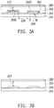
- FIG. 3A and FIG. 3B are respectively cross-sectional schematic views along lines AA and BB in FIG. 2 . Referring to FIG. 2 and FIGs.
- the first interlayer 260 is formed between the first substrate 210 and the first pixel electrode 242 of the pixel electrode 240.
- the pixel electrode 240 is positioned between the first substrate 210 and the display medium layer 290. Due to the first interlayer 260, a minimum vertical distance between the first pixel electrode 242 and the common electrode layer 280 is a first distance G12, a minimum vertical distance between the second pixel electrode 244 and the common electrode layer 280 is a second distance G14, the first distance G12 is different from the second distance G14.
- the electric field applied to the display medium layer 290 corresponding to the first pixel electrode 242 is also different from the electric field applied to the display medium layer 290 corresponding to the second pixel electrode 244, which causes a difference in the transmittance of the display medium layer 290 corresponding to the first pixel electrode 242 and corresponding to the second pixel electrode 244. Accordingly, a color difference as viewed from a direct viewing angle and from a side viewing angle can be reduced, and issues of color shift and insufficient color saturation that exist in the current wide viewing angle technology can be further improved. Moreover, it is not necessary to provide additional active components and relevant driving circuit, or thus a decrease in an aperture ratio of the display device can be avoided without causing difficulty in driving.
- the display medium layer 290 may be a liquid crystal layer. Since the first distance G12 is different from the second distance G14 , the electric field applied to the liquid crystal molecules of the display medium layer 290 corresponding to the first pixel electrode 242 is also different from the electric field applied to the liquid crystal molecules of the display medium layer 290 corresponding to the second pixel electrode 244, which causes a difference in a tilt angle of the liquid crystal molecules corresponding to the first pixel electrode 242 and corresponding to the second pixel electrode 244. Accordingly, color difference as viewed from a direct viewing angle and from a side viewing angle can be reduced, and issues of color shift and insufficient color saturation that exist in the current wide viewing angle technology can be further improved.
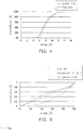
- FIG. 4 is a comparative diagram of a voltage-transmittance relation after driving the liquid crystal molecules corresponding to the first pixel electrode and the second pixel electrode in FIG. 1 .
- FIG. 4 clearly shows that a voltage-transmittance curve of a part of the liquid crystal molecules driven by the first pixel electrode is different from a voltage-transmittance curve a part of the liquid crystal molecules driven by the second pixel electrode.
- the voltage-transmittance curve of the first pixel electrode is shifted leftward from the voltage-transmittance curve of the second pixel electrode. It is implied the first pixel electrode has a lower threshold voltage than the second pixel.
- FIG. 5 is a comparative diagram of gamma curves of the display device of FIG.
- FIG. 5 shows that a gamma curve of the display device of FIG. 1 is closer to an ideal gamma curve 2.2 when compared with a gamma curve of the liquid crystal display device in the prior art.
- a material of the first interlayer 260 is selectively a light-transmitting material.
- the material of the first interlayer 260 may be an insulating material, such as silicon oxide (SiOx) or silicon nitride (SiNx), but the disclosure is not limited hereto.
- the material of the first interlayer 260 may also be an electrically conductive material, such as indium tin oxide (ITO).
- ITO indium tin oxide
- a material of the pixel electrode 240 is selectively a light-transmitting material, such as indium tin oxide (ITO), indium zinc oxide (IZO), aluminum doped zinc oxide (AZO), cadmium tin oxide (CTO), tin oxide (SnO2), zinc oxide (ZnO), etc.
- a material of the common electrode layer 280 is selected to be the same as that of the pixel electrode 240. Moreover, the material of the first interlayer 260 may also be the same as the material of the pixel electrode 240. What is important is to configure the first distance G12 between the first pixel electrode 242 and the common electrode layer 280 to be different from the second distance G14 between the second pixel electrode 244 and the common electrode layer 280.
- a thickness T of the first interlayer 260 is between 0.1 ⁇ m and 0.4 ⁇ m.
- the first interlayer 260 includes a sidewall 262 and a bottom surface 264 connected to the sidewall 262.
- the included angle ⁇ between the sidewall 262 and the bottom surface 264 is between 40° and 90°.
- FIG. 6 is a comparative diagram of a voltage-transmittance relation after the liquid crystal molecules are driven as the included angle and the thickness of the interlayer vary.
- the voltage-transmittance curve of the first pixel electrode moves leftward, which further widens a distance between the voltage-transmittance curve of the first pixel electrode and the voltage-transmittance curve of the second pixel electrode in FIG. 4 , and results in an improved effect of mitigating color shift.
- the voltage-transmittance curve of the first pixel electrode also moves leftward, which similarly further widens the distance between the voltage-transmittance curve of the second pixel electrode and the voltage-transmittance curve of the first pixel electrode, and results in an improved effect of mitigating color shift.
- a portion of the first interlayer 260 positioned between the first pixel electrode 242 and the first substrate includes a first main trunk 260A, a second main trunk 260B, and a plurality of first strip-shaped branches 260C.
- the first main trunk 260A intersects with the second main trunk 260B, and an included angle of the two may be 90° or another appropriate angle.
- the first strip-shaped branches 260C are arranged in parallel in four areas divided by the first main trunk 260A and the second main trunk 260B, and an included angle between one of the first strip-shaped branches 260C and one of the first main trunk 260A and the second main trunk 260B is between 25° ⁇ 65°. For example, in FIG.
- the first strip-shaped branches 260C in the upper-right area divided by the first main trunk 260A and the second main trunk 260B are arranged in parallel at an azimuth angle of 25° to 65°
- the first strip-shaped branches 260C in the lower-right area are arranged in parallel at an azimuth angle of 295° to 340°
- the first strip-shaped branches 260C in the lower-left area are arranged in parallel at an azimuth angle of 205° to 245°
- the first strip-shaped branches 260C in the upper-left area are arranged in parallel at an azimuth angle of 115° to 155°.
- a first gap G26 to expose part of the first substrate means the gap G26 is formed by hollowing out part of the first interlayer to expose part of a layer under than the first interlayer, for example, if the first substrate 210 includes a buffer layer (no shown in the figure) and the buffer layer is directly contacted with the first interlayer, the first gap G26 exposes the buffer layer is one of an embodiment of this disclosure.
- the first substrate no only implied a single plate like glass or flexible plate, but also implied the other layers disposed over the glass or flexible plate.
- first pixel electrode 242 The portion of the first interlayer 260 under each first pixel electrode 242 is approximately in a Union Jack-like pattern.
- first pixel electrode 242 is in a rectangular shape, but in another embodiment, first pixel electrode 242 may also be in other shapes depending on a shape of the sub-pixel area P10.
- the first pixel electrode 242 covers the first main trunk 260A, the second main trunk 260B, and the first strip-shaped branches 260C, and extends to cover the first gap G26.
- the first pixel electrode 242 Since the first pixel electrode 242 is positioned over the first interlayer 260 in a Union Jack-like pattern, a topology of the first pixel electrode 242 varies as the a topology of the first interlayer, so the first pixel electrode 242 has different height from the first substrate, part of the first pixel electrode 242 with higher height is in a Union Jack-like pattern, which further causes the liquid crystal molecules to have a variety of tilt directions and achieves the purpose of a wide viewing angle. Since the first pixel electrode 242 of the pixel electrode 240 is in a complete shape and does not include slits, a phenomenon of dark stripes existing in display can be mitigated.
- Each second pixel electrode 244 of the present embodiment includes a third main trunk 244A, a fourth main trunk 244B, and a plurality of second strip-shaped branches 244C.
- the third main trunk 244A intersects with the fourth main trunk 244B, and an included angle of the two is 90° or another appropriate angle.
- the second strip-shaped branches 244C are arranged in parallel in four areas divided by the third main trunk 244A and the fourth main trunk 244B, and an included angle between one of the second strip-shaped branches 244C and one of the third main trunk 244A and the fourth main trunk 244B is between 25° ⁇ 65°. For example, in FIG.
- the second strip-shaped branches 244C in the upper-right area divided by the third main trunk 244A and the fourth main trunk 244B are arranged in parallel at an azimuth angle of 25° to 65°
- the second strip-shaped branches 244C in the lower-right area are arranged in parallel at an azimuth angle of 295° to 335°
- the second strip-shaped branches 244C in the lower-left area are arranged in parallel at an azimuth angle of 205° to 245°
- the second strip-shaped branches 244C in the upper-left area are arranged in parallel at an azimuth angle of 115° to 155°.
- the second pixel electrode 244 is approximately in a Union Jack-like pattern.
- the first interlayer 260 of the present embodiment includes a plurality of portions separate from each other and is distributed under each first pixel electrode 242. What is important is that, due to the first interlayer 260, the first distance G12 between the first pixel electrode 242 and the common electrode layer 280 is different from the second distance G14 between the second pixel electrode 244 and the common electrode layer 280, as FIG. 3A shows.
- a second gap G16 between the strip-shaped branches 244C of the second pixel electrode 244 is between 3 ⁇ m and 10 ⁇ m and exposes the first substrate 210.
- FIG. 7 is a comparative diagram of a voltage-transmittance relation after the liquid crystal molecules are driven as the gap between the strip-shaped branches of the second pixel electrode of the pixel electrode varies.
- FIG. 7 shows that as the gap between the strip-shaped branches of the second pixel electrode increases, the voltage-transmittance curve of the second pixel electrode moves rightward, which further widens a distance between the voltage-transmittance curve of the first pixel electrode and the voltage-transmittance curve of the second pixel electrode in FIG. 4 and results in an improved effect of mitigating color shift.
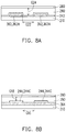
- FIG. 8A and FIG. 8B are respectively cross-sectional schematic views at the first pixel electrode and the second pixel electrode of the pixel electrode of the display device according to another embodiment of the disclosure.
- the display device of the present embodiment is similar to that of the embodiment of FIGs. 3A and 3B , and the differences between the two are described here.
- FIG. 8A is basically identical to FIG. 3A
- the interlayer includes a first interlayer 362 and a second interlayer 364. Materials of the first interlayer 362 and the second interlayer 364 are similar to that of the first interlayer 260 in FIG. 2 .
- a shape and a position of the first interlayer 362 are also similar to those of the first interlayer 260 in FIG. 2 (namely, being between the first pixel electrode 242 and the first substrate 210).
- the first interlayer 362 includes a plurality of first strip-shaped branches 362A. Adjacent two of the first strip-shaped branches 362A form a first gap G22 to expose part of the first substrate 210.
- a first gap G22 to expose part of the first substrate means the gap G22 is formed by hollowing out part of the first interlayer to expose part of a layer under than the first interlayer, for example, if the first substrate 210 includes a buffer layer (no shown in the figure) and the buffer layer is directly contacted with the first interlayer, the first gap G22 exposes the buffer layer is one of an embodiment of this disclosure.
- the first substrate no only implied a single plate like glass or flexible plate, but also implied the other layers disposed over the glass or flexible plate.
- the first pixel electrode 242 extends to cover the first gap G22.
- the second interlayer 364 is fully distributed under the second pixel electrode 244.
- the second pixel electrode 244 is raised in entirety by the second interlayer 364.
- the second gap G16 between the second strip-shaped branches 244C of the second pixel electrode 244 exposes part of the second interlayer 364.
- a maximum vertical distance between the first pixel electrode 242 and the common electrode layer 280 is a first distance G24
- a maximum vertical distance between the second pixel electrode 244 and the common electrode layer 280 is a second distance G18
- the first distance G24 is still different from the second distance G18.
- a difference between the first distance G24 and the second distance G18 is 0.1 ⁇ m to 0.4 ⁇ m.
- the display device of the present embodiment similarly improves issues of color shift and insufficient color saturation that exist in the current wide viewing angle technology or can avoid a decrease in an aperture ratio of the display device without causing difficulty in driving. Moreover, as the second maximum distance G18 between the second pixel electrode 244 and the common electrode layer 280 is decreased, the wide viewing angle effect further becomes more significant.
- the entire pixel electrode in the sub-pixel area has the same electric potential.
- the arrangement of the interlayer enables the distance between the first pixel electrode of the pixel electrode and the common electrode layer to be different from the distance between the second pixel electrode of the pixel electrode and the common electrode layer. Accordingly, without providing additional active components and relevant driving circuits, brightness presented by the first pixel electrode and that by the second pixel electrode can still be different. Thereby, the issues of color shift and insufficient color saturation can be mitigated, and meanwhile a process yield rate or the aperture ratio of the display device can be improved.
Landscapes
- Physics & Mathematics (AREA)
- Nonlinear Science (AREA)
- Mathematical Physics (AREA)
- Chemical & Material Sciences (AREA)
- Crystallography & Structural Chemistry (AREA)
- General Physics & Mathematics (AREA)
- Optics & Photonics (AREA)
- Geometry (AREA)
- Spectroscopy & Molecular Physics (AREA)
- Liquid Crystal (AREA)
- Engineering & Computer Science (AREA)
- Microelectronics & Electronic Packaging (AREA)
Abstract
Description
- The disclosure relates to a display device.
- Nowadays, the market demands the liquid crystal display device to develop its functions towards high contrast ratio, no gray scale inversion, low color shift, high luminance, full color, high color saturation, high response speed, and a wide viewing angle. Currently, the technologies capable of meeting the requirement of a wide viewing angle include the twist nematic (TN) liquid crystal having a wide viewing film, the in-plane switching (IPS) liquid crystal display device, the fringe field switching liquid crystal display device, and the multi-domain vertical alignment (MVA) liquid crystal display device. However, when viewing a vertical alignment liquid crystal display device, due to the birefringence properties of liquid crystal molecules, there exists a phenomenon where colors seen from a side viewing angle are different from those seen from a direct viewing angle; namely, a phenomenon of color shift occurs.
- The technology of Low color shift is developed for solving this problem, different voltages separately provided to two separate pixel electrodes in a the sub-pixel area, at least one more transistor is need to control the pixel electrodes, as a result, a tilt degree of liquid crystal molecules driven by the separate pixel electrodes are also different to mitigate the issues of color shift and insufficient color saturation. However, such design increases a number of the thin film transistors and meanwhile increases a number of the scan lines. It not only increases a probability of lowering the process yield rate, but also lowers the aperture rate of the liquid crystal display device.
- The disclosure provides a display device capable of solving issues of a low process yield rate or a low aperture ratio in the current wide viewing angle technology.
- According to one embodiment of the disclosure, the display device includes a first substrate, at least two scan lines, at least two data lines, at least a pixel electrode, at least an active component, a first interlayer, a second substrate, a common electrode layer, and a display medium layer. The scan lines, the data lines, the pixel electrode, and the active component are disposed over the first substrate. Adjacent two of the scan lines and adjacent two of the data lines intersect to define a sub-pixel area. The active component is electrically connected to one of the scan lines. The pixel electrode is electrically connected to the active component. The pixel electrode includes a first pixel electrode and a second pixel electrode having the same electric potential. The first interlayer is formed between the first substrate and the first pixel electrode of the pixel electrode. The first interlayer includes a plurality of first strip-shaped branches. Adjacent two of the first strip-shaped branches form a first gap to expose part of the first substrate. The common electrode layer is disposed over the second substrate. The display medium layer is disposed between the first substrate and the second substrate. The pixel electrode is positioned between the first substrate and the display medium layer. The first pixel electrode extends to cover the first gap. A maximum vertical distance between the first pixel electrode and the common electrode layer is a first distance. A maximum vertical distance between the second pixel electrode and the common electrode layer is a second distance. A difference between the first distance and the second distance is 0.1 µm to 0.4 µm.
- In the display device according to one embodiment of the disclosure, the second pixel electrode includes a plurality of second strip-shaped branches, wherein adjacent two of the strip-shaped branches form a second gap.
- In the display device according to one embodiment of the disclosure, the display device further includes a second interlayer disposed between the first substrate and the second pixel electrode.
- In the display device according to one embodiment of the disclosure, the second gap exposes part of the second interlayer.
- In the display device according to one embodiment of the disclosure, a material of at least one of the first interlayer and the second interlayer is identical to a material of the pixel electrode.
- In the display device according to one embodiment of the disclosure, the material of at least one of the first interlayer and the second interlayer is an insulating material.
- In the display device according to one embodiment of the disclosure, the first interlayer further includes a first main trunk and a second main trunk, the first main trunk and the second main trunk intersects. Each of the first strip-shaped branches connects to one of the first main trunk and the second main trunk. An included angle between one of the first strip-shaped branches and one of the first main trunk and the second main trunk is between 25° and 65°.
- In the display device according to one embodiment of the disclosure, the second pixel electrode includes a third main trunk and a fourth main trunk. The third main trunk and the fourth main trunk intersects. Each of the second strip-shaped branches connects to one of the third main trunk and the fourth main trunk. An included angle between one of the second strip-shaped branches and one of the third main trunk and the fourth main trunk is between 25° and 65°.
- In the display device according to one embodiment of the disclosure, the first pixel electrode directly connects to the second pixel electrode.
- In the display device according to one embodiment of the disclosure, the first interlayer comprises a sidewall and a bottom surface connected to the sidewall. An included angle between the sidewall and the bottom surface is between 40° and 90°.
- According to another embodiment of the disclosure, the display device includes a first substrate, at least two scan lines, at least two data lines, at least a pixel electrode, at least an active component, a first interlayer, a second substrate, a common electrode layer, and a display medium layer. The scan lines, the data lines, the pixel electrode, and the active component are disposed over the first substrate. Adjacent two of the scan lines and adjacent two of the data lines intersect to define a sub-pixel area. The active component is electrically connected to one of the scan line. The pixel electrode is electrically connected to the active component. The pixel electrode includes a first pixel electrode and a second pixel electrode having the same electric potential. The first interlayer is formed between the first substrate and the first pixel electrode of the pixel electrode. The first interlayer includes a plurality of first strip-shaped branches. Adjacent two of the first strip-shaped branches form a first gap to expose part of the first substrate. The common electrode layer is disposed over the second substrate. The display medium layer is disposed between the first substrate and the second substrate. The pixel electrode is positioned between the first substrate and the display medium layer. The first pixel electrode extends to cover the first gap. The second pixel electrode includes a plurality of second strip-shaped branches. Adjacent two of the second strip-shaped branches form a second gap. A minimum distance between the first pixel electrode and the common electrode layer is a third distance. A minimum distance between the second pixel electrode and the common electrode layer is a fourth distance. The third distance is different from the fourth distance.
- In the display device according to one embodiment of the disclosure, a difference between the third distance and the fourth distance is 0.1 µm to 0.4 µm.
- In the display device according to one embodiment of the disclosure, the second gap is between 3 µm and 10 µm.
- In the display device according to one embodiment of the disclosure, a thickness of the first interlayer is between 0.1 µm and 0.4 µm.
- In the display device according to one embodiment of the disclosure, the first interlayer includes a sidewall and a bottom surface connected to the sidewall. An included angle formed between the sidewall and the bottom surface is between 40° and 90°.
- In the display device according to one embodiment of the disclosure, the first interlayer further includes a first main trunk and a second main trunk. The first main trunk and the second main trunk intersects. Each of the first strip-shaped branches connects to one of the first main trunk and the second main trunk. An included angle between one of the first strip-shaped branches and one of the first main trunk and the second main trunk is between 25° and 65°.
- In the display device according to one embodiment of the disclosure, the second pixel electrode includes a third main trunk and a fourth main trunk. The third main trunk and the fourth main trunk intersects. Each of the second strip-shaped branches connects to one of the third main trunk and the fourth main trunk. An included angle between one of the second strip-shaped branches and one of the third main trunk and the fourth main trunk is between 25° and 65°.
- In the display device according to one embodiment of the disclosure, the first pixel electrode directly connects to the second pixel electrode.
- In light of the above, the pixel electrode (include first pixel electrode and second pixel electrode) of the display device of the disclosure has substantially the same electric potential. However, through the design of the interlayer, the distance between the first pixel electrode of the pixel electrode and the common electrode layer is different from the distance between the second pixel electrode of the pixel electrode and the common electrode layer. Accordingly, without increasing a number of the active component, brightness presented by the first pixel electrode and by the second pixel electrode can still be different to mitigate the issues of color shift and insufficient color saturation. Thereby, the process yield rate or the aperture ratio of the display device can be improved.
-
-
FIG. 1 is a cross-sectional simplified schematic view of a display device according to one embodiment of the disclosure. -
FIG. 2 is a top view of a single sub-pixel area of the display device ofFIG. 1 . -
FIG. 3A and FIG. 3B are respectively cross-sectional schematic views along lines AA and BB inFIG. 2 . -
FIG. 4 is a comparative diagram of a voltage-transmittance relation after driving liquid crystal molecules of a first pixel electrode and a second pixel electrode of a pixel electrode inFIG. 1 . -
FIG. 5 is a comparative diagram of gamma curves of the display device ofFIG. 1 and a liquid crystal display device in the prior art. -
FIG. 6 is a comparative diagram of a voltage-transmittance relation after the liquid crystal molecules are driven as an included angle at a bottom of an edge of an interlayer and a thickness of the interlayer vary. -
FIG. 7 is a comparative diagram of a voltage-transmittance relation after the liquid crystal molecules are driven as a gap between second strip-shaped branches of the second pixel electrode of the pixel electrode varies. -
FIG. 8A and FIG. 8B are respectively cross-sectional schematic views at the first pixel electrode and the second pixel electrode of the pixel electrode of the display device according to another embodiment of the disclosure. - Reference will now be made in detail to the exemplary embodiments of the disclosure, examples of which are illustrated in the accompanying drawings. Wherever possible, the same reference numbers are used in the drawings and the description to refer to the same or like parts.
-
FIG. 1 is a cross-sectional simplified schematic view of a display device according to one embodiment of the disclosure.FIG. 2 is a top view of a single sub-pixel area of the display device ofFIG. 1 . Referring toFIGs. 1 and2 , adisplay device 200 according to one embodiment of the disclosure includes afirst substrate 210, at least twoscan lines 220, at least twodata lines 230, at least apixel electrode 240, at least anactive component 250, afirst interlayer 260, a second substrate 270, acommon electrode layer 280, and adisplay medium layer 290.FIG. 2 only illustrates one single sub-pixel area. Upon referring toFIG. 2 , an arrangement of at least two ormore scan lines 220, at least two ormore data lines 230, a plurality ofpixel electrodes 240, and a plurality ofactive components 250 are not be repeated here. Thescan lines 220, thedata lines 230, thepixel electrode 240, and theactive component 250 are all disposed over thefirst substrate 210. Adjacent two of thescan lines 220 and adjacent two of thedata lines 230 intersect to define a sub-pixel area P10. Theactive component 250 is electrically connected to one of the scan lines 220. Thepixel electrode 240 is electrically connected to theactive component 250 and can receive data signal sent from the data lines 230. Thecommon electrode layer 280 is disposed over the second substrate 270. Thedisplay medium layer 290 is disposed between thefirst substrate 210 and the second substrate 270 (in other words, between thefirst substrate 210 and the common electrode layer 280). When a threshold voltage is inputted through thescan lines 220 to turn on theactive component 250, the data signal sent by thedata lines 240 can be sent to thepixel electrode 240 via theactive component 250. Through an electric field generated by a voltage difference between thepixel electrode 240 and thecommon electrode layer 280, thedisplay medium layer 290 is driven to control transmittance variations and thereby generate display effect. - Referring to
FIG. 2 , thepixel electrode 240 includes afirst pixel electrode 242 and asecond pixel electrode 244 substantially having the same electric potential. In the present embodiment, thefirst pixel electrode 242 and thesecond pixel electrode 244 are directly connected to each other. However, thefirst pixel electrode 242 and thesecond pixel electrode 244 may also be electrically connected via other conductive paths, as long as thefirst pixel electrode 242 and thesecond pixel electrode 244 substantially have the same electric potential.FIG. 3A and FIG. 3B are respectively cross-sectional schematic views along lines AA and BB inFIG. 2 . Referring toFIG. 2 andFIGs. 3A and 3B , thefirst interlayer 260 is formed between thefirst substrate 210 and thefirst pixel electrode 242 of thepixel electrode 240. Thepixel electrode 240 is positioned between thefirst substrate 210 and thedisplay medium layer 290. Due to thefirst interlayer 260, a minimum vertical distance between thefirst pixel electrode 242 and thecommon electrode layer 280 is a first distance G12, a minimum vertical distance between thesecond pixel electrode 244 and thecommon electrode layer 280 is a second distance G14, the first distance G12 is different from the second distance G14. Since the first distance G12 is different from the second distance G14, the electric field applied to thedisplay medium layer 290 corresponding to thefirst pixel electrode 242 is also different from the electric field applied to thedisplay medium layer 290 corresponding to thesecond pixel electrode 244, which causes a difference in the transmittance of thedisplay medium layer 290 corresponding to thefirst pixel electrode 242 and corresponding to thesecond pixel electrode 244. Accordingly, a color difference as viewed from a direct viewing angle and from a side viewing angle can be reduced, and issues of color shift and insufficient color saturation that exist in the current wide viewing angle technology can be further improved. Moreover, it is not necessary to provide additional active components and relevant driving circuit, or thus a decrease in an aperture ratio of the display device can be avoided without causing difficulty in driving. - For example, the
display medium layer 290 may be a liquid crystal layer. Since the first distance G12 is different from the second distance G14 , the electric field applied to the liquid crystal molecules of thedisplay medium layer 290 corresponding to thefirst pixel electrode 242 is also different from the electric field applied to the liquid crystal molecules of thedisplay medium layer 290 corresponding to thesecond pixel electrode 244, which causes a difference in a tilt angle of the liquid crystal molecules corresponding to thefirst pixel electrode 242 and corresponding to thesecond pixel electrode 244. Accordingly, color difference as viewed from a direct viewing angle and from a side viewing angle can be reduced, and issues of color shift and insufficient color saturation that exist in the current wide viewing angle technology can be further improved. -
FIG. 4 is a comparative diagram of a voltage-transmittance relation after driving the liquid crystal molecules corresponding to the first pixel electrode and the second pixel electrode inFIG. 1 .FIG. 4 clearly shows that a voltage-transmittance curve of a part of the liquid crystal molecules driven by the first pixel electrode is different from a voltage-transmittance curve a part of the liquid crystal molecules driven by the second pixel electrode. The voltage-transmittance curve of the first pixel electrode is shifted leftward from the voltage-transmittance curve of the second pixel electrode. It is implied the first pixel electrode has a lower threshold voltage than the second pixel.FIG. 5 is a comparative diagram of gamma curves of the display device ofFIG. 1 and a liquid crystal display device in the prior art.FIG. 5 shows that a gamma curve of the display device ofFIG. 1 is closer to an ideal gamma curve 2.2 when compared with a gamma curve of the liquid crystal display device in the prior art. This proves that the design of the display device of the present embodiment can indeed achieve the purposes of mitigating the color shift phenomenon and enhancing color saturation. - The following describes other selective variations of the technical means of the disclosure, but the disclosure is not limited hereto.
- A material of the
first interlayer 260 is selectively a light-transmitting material. On the other hand, the material of thefirst interlayer 260 may be an insulating material, such as silicon oxide (SiOx) or silicon nitride (SiNx), but the disclosure is not limited hereto. The material of thefirst interlayer 260 may also be an electrically conductive material, such as indium tin oxide (ITO). A material of thepixel electrode 240 is selectively a light-transmitting material, such as indium tin oxide (ITO), indium zinc oxide (IZO), aluminum doped zinc oxide (AZO), cadmium tin oxide (CTO), tin oxide (SnO2), zinc oxide (ZnO), etc. A material of thecommon electrode layer 280 is selected to be the same as that of thepixel electrode 240. Moreover, the material of thefirst interlayer 260 may also be the same as the material of thepixel electrode 240. What is important is to configure the first distance G12 between thefirst pixel electrode 242 and thecommon electrode layer 280 to be different from the second distance G14 between thesecond pixel electrode 244 and thecommon electrode layer 280. - Referring to
FIG. 3A , a thickness T of thefirst interlayer 260 is between 0.1 µm and 0.4 µm. Specifically, thefirst interlayer 260 includes asidewall 262 and abottom surface 264 connected to thesidewall 262. The included angle θ between thesidewall 262 and thebottom surface 264 is between 40° and 90°.FIG. 6 is a comparative diagram of a voltage-transmittance relation after the liquid crystal molecules are driven as the included angle and the thickness of the interlayer vary.FIG. 6 shows that as the thickness of the interlayer increases, the voltage-transmittance curve of the first pixel electrode moves leftward, which further widens a distance between the voltage-transmittance curve of the first pixel electrode and the voltage-transmittance curve of the second pixel electrode inFIG. 4 , and results in an improved effect of mitigating color shift. Moreover, as the included angle formed between the sidewall and the bottom surface of the interlayer increases, the voltage-transmittance curve of the first pixel electrode also moves leftward, which similarly further widens the distance between the voltage-transmittance curve of the second pixel electrode and the voltage-transmittance curve of the first pixel electrode, and results in an improved effect of mitigating color shift. - Next, referring to
FIG. 2 , a portion of thefirst interlayer 260 positioned between thefirst pixel electrode 242 and the first substrate includes a firstmain trunk 260A, a secondmain trunk 260B, and a plurality of first strip-shapedbranches 260C. The firstmain trunk 260A intersects with the secondmain trunk 260B, and an included angle of the two may be 90° or another appropriate angle. The first strip-shapedbranches 260C are arranged in parallel in four areas divided by the firstmain trunk 260A and the secondmain trunk 260B, and an included angle between one of the first strip-shapedbranches 260C and one of the firstmain trunk 260A and the secondmain trunk 260B is between 25°∼65°. For example, inFIG. 2 , the first strip-shapedbranches 260C in the upper-right area divided by the firstmain trunk 260A and the secondmain trunk 260B are arranged in parallel at an azimuth angle of 25° to 65°, the first strip-shapedbranches 260C in the lower-right area are arranged in parallel at an azimuth angle of 295° to 340°, the first strip-shapedbranches 260C in the lower-left area are arranged in parallel at an azimuth angle of 205° to 245°, and the first strip-shapedbranches 260C in the upper-left area are arranged in parallel at an azimuth angle of 115° to 155°. Referring toFIG. 3 , adjacent two of the first strip-shapedbranches 260C form a first gap G26 to expose part of thefirst substrate 210. It have to say that "a first gap G26 to expose part of the first substrate" means the gap G26 is formed by hollowing out part of the first interlayer to expose part of a layer under than the first interlayer, for example, if thefirst substrate 210 includes a buffer layer (no shown in the figure) and the buffer layer is directly contacted with the first interlayer, the first gap G26 exposes the buffer layer is one of an embodiment of this disclosure. In another words, the first substrate no only implied a single plate like glass or flexible plate, but also implied the other layers disposed over the glass or flexible plate. The portion of thefirst interlayer 260 under eachfirst pixel electrode 242 is approximately in a Union Jack-like pattern. In this embodiment,first pixel electrode 242 is in a rectangular shape, but in another embodiment,first pixel electrode 242 may also be in other shapes depending on a shape of the sub-pixel area P10. Thefirst pixel electrode 242 covers the firstmain trunk 260A, the secondmain trunk 260B, and the first strip-shapedbranches 260C, and extends to cover the first gap G26. Since thefirst pixel electrode 242 is positioned over thefirst interlayer 260 in a Union Jack-like pattern, a topology of thefirst pixel electrode 242 varies as the a topology of the first interlayer, so thefirst pixel electrode 242 has different height from the first substrate, part of thefirst pixel electrode 242 with higher height is in a Union Jack-like pattern, which further causes the liquid crystal molecules to have a variety of tilt directions and achieves the purpose of a wide viewing angle. Since thefirst pixel electrode 242 of thepixel electrode 240 is in a complete shape and does not include slits, a phenomenon of dark stripes existing in display can be mitigated. Eachsecond pixel electrode 244 of the present embodiment includes a thirdmain trunk 244A, a fourthmain trunk 244B, and a plurality of second strip-shaped branches 244C. The thirdmain trunk 244A intersects with the fourthmain trunk 244B, and an included angle of the two is 90° or another appropriate angle. The second strip-shaped branches 244C are arranged in parallel in four areas divided by the thirdmain trunk 244A and the fourthmain trunk 244B, and an included angle between one of the second strip-shaped branches 244C and one of the thirdmain trunk 244A and the fourthmain trunk 244B is between 25°∼65°. For example, inFIG. 2 , the second strip-shaped branches 244C in the upper-right area divided by the thirdmain trunk 244A and the fourthmain trunk 244B are arranged in parallel at an azimuth angle of 25° to 65°, the second strip-shaped branches 244C in the lower-right area are arranged in parallel at an azimuth angle of 295° to 335°, the second strip-shaped branches 244C in the lower-left area are arranged in parallel at an azimuth angle of 205° to 245°, and the second strip-shaped branches 244C in the upper-left area are arranged in parallel at an azimuth angle of 115° to 155°. Thesecond pixel electrode 244 is approximately in a Union Jack-like pattern. - The
first interlayer 260 of the present embodiment includes a plurality of portions separate from each other and is distributed under eachfirst pixel electrode 242. What is important is that, due to thefirst interlayer 260, the first distance G12 between thefirst pixel electrode 242 and thecommon electrode layer 280 is different from the second distance G14 between thesecond pixel electrode 244 and thecommon electrode layer 280, asFIG. 3A shows. In the present embodiment, a second gap G16 between the strip-shaped branches 244C of thesecond pixel electrode 244 is between 3 µm and 10µm and exposes thefirst substrate 210.FIG. 7 is a comparative diagram of a voltage-transmittance relation after the liquid crystal molecules are driven as the gap between the strip-shaped branches of the second pixel electrode of the pixel electrode varies.FIG. 7 shows that as the gap between the strip-shaped branches of the second pixel electrode increases, the voltage-transmittance curve of the second pixel electrode moves rightward, which further widens a distance between the voltage-transmittance curve of the first pixel electrode and the voltage-transmittance curve of the second pixel electrode inFIG. 4 and results in an improved effect of mitigating color shift. -
FIG. 8A and FIG. 8B are respectively cross-sectional schematic views at the first pixel electrode and the second pixel electrode of the pixel electrode of the display device according to another embodiment of the disclosure. Referring toFIGs. 8A and 8B , the display device of the present embodiment is similar to that of the embodiment ofFIGs. 3A and 3B , and the differences between the two are described here.FIG. 8A is basically identical toFIG. 3A , while inFIG. 8B , the interlayer includes a first interlayer 362 and asecond interlayer 364. Materials of the first interlayer 362 and thesecond interlayer 364 are similar to that of thefirst interlayer 260 inFIG. 2 . A shape and a position of the first interlayer 362 are also similar to those of thefirst interlayer 260 inFIG. 2 (namely, being between thefirst pixel electrode 242 and the first substrate 210). The first interlayer 362 includes a plurality of first strip-shaped branches 362A. Adjacent two of the first strip-shaped branches 362A form a first gap G22 to expose part of thefirst substrate 210. It have to say that "a first gap G22 to expose part of the first substrate" means the gap G22 is formed by hollowing out part of the first interlayer to expose part of a layer under than the first interlayer, for example, if thefirst substrate 210 includes a buffer layer (no shown in the figure) and the buffer layer is directly contacted with the first interlayer, the first gap G22 exposes the buffer layer is one of an embodiment of this disclosure. In another words, the first substrate no only implied a single plate like glass or flexible plate, but also implied the other layers disposed over the glass or flexible plate. Thefirst pixel electrode 242 extends to cover the first gap G22. Thesecond interlayer 364 is fully distributed under thesecond pixel electrode 244. In other words, thesecond pixel electrode 244 is raised in entirety by thesecond interlayer 364. The second gap G16 between the second strip-shaped branches 244C of thesecond pixel electrode 244 exposes part of thesecond interlayer 364. However, due to the first interlayer 362 and thesecond interlayer 364, a maximum vertical distance between thefirst pixel electrode 242 and thecommon electrode layer 280 is a first distance G24, a maximum vertical distance between thesecond pixel electrode 244 and thecommon electrode layer 280 is a second distance G18, the first distance G24 is still different from the second distance G18. A difference between the first distance G24 and the second distance G18 is 0.1 µm to 0.4 µm. Accordingly, the display device of the present embodiment similarly improves issues of color shift and insufficient color saturation that exist in the current wide viewing angle technology or can avoid a decrease in an aperture ratio of the display device without causing difficulty in driving. Moreover, as the second maximum distance G18 between thesecond pixel electrode 244 and thecommon electrode layer 280 is decreased, the wide viewing angle effect further becomes more significant. - In light of the above, the entire pixel electrode in the sub-pixel area has the same electric potential. However, the arrangement of the interlayer enables the distance between the first pixel electrode of the pixel electrode and the common electrode layer to be different from the distance between the second pixel electrode of the pixel electrode and the common electrode layer. Accordingly, without providing additional active components and relevant driving circuits, brightness presented by the first pixel electrode and that by the second pixel electrode can still be different. Thereby, the issues of color shift and insufficient color saturation can be mitigated, and meanwhile a process yield rate or the aperture ratio of the display device can be improved.
Claims (18)
- A display device (200) comprising:a first substrate (210);at least two scan lines (220), at least two data lines (230), at least a pixel electrode (240), and at least an active component (250), disposed over the first substrate (210), wherein adjacent two of the scan lines (220) and adjacent two of the data lines (230) intersect to define a sub-pixel area (P10), the active component (250) is electrically connected to one of the scan lines (220), the pixel electrode (240) is electrically connected to the active component (250), and the pixel electrode (240) comprises a first pixel electrode (242) and a second pixel electrode (244) having the same electric potential;a first interlayer (362) disposed between the first substrate (210) and the first pixel electrode (242), wherein the first interlayer (362) comprises a plurality of first strip-shaped branches (362A), wherein adjacent two of the first strip-shaped branches (362A) form a first gap (G22) to expose part of the first substrate (210);a second substrate (270);a common electrode layer (280) disposed over the second substrate (270); anda display medium layer (290) disposed between the first substrate (210) and the second substrate (270), wherein the pixel electrode (240) is positioned between the first substrate (210) and the display medium layer (290), the first pixel electrode (242) extends to cover the first gap (G22), a maximum vertical distance between the first pixel electrode (242) and the common electrode layer (280) is a first distance (G24), a maximum vertical distance between the second pixel electrode (244) and the common electrode layer (280) is a second distance (G18), and a difference between the first distance (G24) and the second distance (G18) is 0.1 µm to 0.4 µm.
- The display device (200) according to claim 1, wherein the second pixel electrode (244) comprises a plurality of second strip-shaped branches (244C), wherein adjacent two of the second strip-shaped branches (244C) form a second gap (G16).
- The display device (200) according to claim 2, further comprising a second interlayer (364) disposed between the first substrate (210) and the second pixel electrode (244).
- The display device (200) according to claim 3, wherein the second gap (G16) exposes part of the second interlayer (364).
- The display device (200) according to claim 3 or 4, wherein a material of at least one of the first interlayer (362) and the second interlayer (364) is identical to a material of the pixel electrode (240).
- The display device (200) according to claim 3 or 4, wherein a material of at least one of the first interlayer (362) and the second interlayer (364) is an insulating material.
- The display device (200) according to one of the claims 3-6, wherein the first interlayer (362) further includes a first main trunk(260A) and a second main trunk(260B), the first main trunk(260A) and the second main trunk(260B) intersects, each of the first strip-shaped branches (362A) connects to one of the first main trunk(260A) and the second main trunk(260B), an included angle between one of the first strip-shaped branches (362A) and one of the first main trunk(260A) and the second main trunk(260B) is between 25° and 65°.
- The display device (200) according to one of the claims 2-7, wherein the second pixel electrode (244) includes a third main trunk (244A) and a fourth main trunk (244B), the third main trunk (244A) and the fourth main trunk (244B) intersects, each of the second strip-shaped branches (244C) connects to one of the third main trunk (244A) and the fourth main trunk (244B), an included angle between one of the second strip-shaped branches (244C) and one of the third main trunk (244A) and the fourth main trunk (244B) is between 25° and 65°.
- The display device (200) according to one of the preceding claims, wherein the first pixel electrode (242) directly connects to the second pixel electrode (244).
- The display device (200) according to one of the preceding claims, wherein the first interlayer (260) comprises a sidewall (262) and a bottom surface (264) connected to the sidewall (262), and an included angle (θ) between the sidewall (262) and the bottom surface (264) is between 40° and 90°.
- A display device (200) comprising:a first substrate (210);at least two scan lines (220), at least two data lines (230), at least a pixel electrode (240), and at least an active component (250), disposed over the first substrate (210), wherein adjacent two of the scan lines (220) and adjacent two of the data lines (230) intersect to define a sub-pixel area (P10), the active component (250) is electrically connected to one of the scan lines (220), the pixel electrode (240) is electrically connected to the active component (250), and the pixel electrode (240) comprises a first pixel electrode (242) and a second pixel electrode (244) having the same electric potential;a first interlayer (260) formed between the first substrate (210) and the first pixel electrode (242) of the pixel electrode (240), wherein the first interlayer (260) comprises a plurality of first strip-shaped branches (260C), wherein adjacent two of the first strip-shaped branches (260C) form a first gap (G26) to expose part of the first substrate (210);a second substrate (270);a common electrode layer (280) disposed over the second substrate (270); anda display medium layer (290) disposed between the first substrate (210) and the second substrate (270), wherein the pixel electrode (240) is positioned between the first substrate (210) and the display medium layer (290), the first pixel electrode (242) extends to cover the first gap (G26), the second pixel electrode (244) comprises a plurality of second strip-shaped branches (244C), wherein adjacent two of the second strip-shaped branches (244C) form a second gap (G16), and a minimum vertical distance between the first pixel electrode (242) and the common electrode layer (280) is a first distance (G12), a minimum vertical distance between the second pixel electrode (244) and the common electrode layer (280) is a second distance (G14), the first distance (G12) is different from the second distance.
- The display device (200) according to claim 11, a difference between the first distance (G12) and the second distance (G14) is 0.1 µm to 0.4 µm.
- The display device (200) according to claim 11 or 12, wherein the second gap (G16) is between 3 µm and 10 µm.
- The display device (200) according to claim 11, 12 or 13 wherein a thickness (T) of the first interlayer (260) is between 0.1 µm and 0.4 µm.
- The display device (200) according to one of the claims 11-14, wherein the first interlayer (260) comprises a sidewall (262) and a bottom surface (264) connected to the sidewall (262), and an included angle (θ) between the sidewall (262) and the bottom surface (264) is between 40° and 90°.
- The display device (200) according to one of the claims 11-14, wherein the first interlayer (260) further includes a first main trunk(260A) and a second main trunk(260B), the first main trunk(260A) and the second main trunk(260B) intersects, each of the first strip-shaped branches (260C) connects to one of the first main trunk(260A) and the second main trunk(260B), an included angle between one of the first strip-shaped branches (260C) and one of the first main trunk(260A) and the second main trunk(260B) is between 25° and 65°.
- The display device (200) according to one of the claims 11-14, wherein the second pixel electrode (244) includes a third main trunk (244A) and a fourth main trunk (244B), the third main trunk (244A) and the fourth main trunk (244B) intersects, each of the second strip-shaped branches (244C) connects to one of the third main trunk (244A) and the fourth main trunk (244B), an included angle between one of the second strip-shaped branches (244C) and one of the third main trunk (244A) and the fourth main trunk (244B) is between 25° and 65°.
- The display device (200) according to one of the claims 11-14, the first pixel electrode (242) directly connects to the second pixel electrode (244).
Applications Claiming Priority (1)
| Application Number | Priority Date | Filing Date | Title |
|---|---|---|---|
| CN201511006036.1A CN106932969B (en) | 2015-12-29 | 2015-12-29 | Display device |
Publications (2)
| Publication Number | Publication Date |
|---|---|
| EP3187924A1 true EP3187924A1 (en) | 2017-07-05 |
| EP3187924B1 EP3187924B1 (en) | 2021-03-31 |
Family
ID=57570832
Family Applications (1)
| Application Number | Title | Priority Date | Filing Date |
|---|---|---|---|
| EP16205407.6A Active EP3187924B1 (en) | 2015-12-29 | 2016-12-20 | Display device |
Country Status (3)
| Country | Link |
|---|---|
| US (1) | US10048547B2 (en) |
| EP (1) | EP3187924B1 (en) |
| CN (1) | CN106932969B (en) |
Families Citing this family (9)
| Publication number | Priority date | Publication date | Assignee | Title |
|---|---|---|---|---|
| CN106783891B (en) * | 2017-02-10 | 2019-09-13 | 京东方科技集团股份有限公司 | Array substrate and control method thereof |
| KR102317070B1 (en) * | 2017-08-02 | 2021-10-25 | 삼성디스플레이 주식회사 | Liquid crystal display device |
| CN109283755B (en) * | 2018-08-15 | 2022-01-04 | 咸阳彩虹光电科技有限公司 | Pixel structure, pixel unit and display panel |
| CN209343106U (en) * | 2018-12-04 | 2019-09-03 | 惠科股份有限公司 | Display panel and display device |
| CN109407380B (en) * | 2018-12-05 | 2021-06-11 | 惠科股份有限公司 | Display panel, manufacturing method thereof and display device |
| CN110174787B (en) * | 2019-05-06 | 2021-11-30 | 惠科股份有限公司 | Array substrate, manufacturing method thereof and display device |
| CN110928094B (en) * | 2019-12-31 | 2020-12-15 | 成都中电熊猫显示科技有限公司 | Array substrate and liquid crystal panel |
| CN111338134A (en) * | 2020-03-13 | 2020-06-26 | Tcl华星光电技术有限公司 | Pixel electrode structure and liquid crystal display panel |
| TWI812196B (en) * | 2022-04-29 | 2023-08-11 | 宏碁股份有限公司 | Display device |
Citations (4)
| Publication number | Priority date | Publication date | Assignee | Title |
|---|---|---|---|---|
| US20090128765A1 (en) * | 2007-11-16 | 2009-05-21 | Samsung Electronics Co., Ltd. | Display device |
| US20110317104A1 (en) * | 2010-04-06 | 2011-12-29 | Sony Corporation | Liquid crystal display and method of manufacturing liquid crystal display |
| US20140320794A1 (en) * | 2013-04-25 | 2014-10-30 | Shenzhen China Star Optoelectronics Technology Co., Ltd. | Liquid crystal panel |
| US20150103281A1 (en) * | 2010-12-14 | 2015-04-16 | Samsung Display Co., Ltd. | Liquid crystal display to increase side view visibility |
Family Cites Families (2)
| Publication number | Priority date | Publication date | Assignee | Title |
|---|---|---|---|---|
| JP4248835B2 (en) * | 2002-04-15 | 2009-04-02 | シャープ株式会社 | Substrate for liquid crystal display device and liquid crystal display device including the same |
| KR101814208B1 (en) * | 2010-04-06 | 2018-01-02 | 소니 주식회사 | Liquid crystal diplay and method of manufacturing liquid crystal display |
-
2015
- 2015-12-29 CN CN201511006036.1A patent/CN106932969B/en active Active
-
2016
- 2016-12-08 US US15/372,397 patent/US10048547B2/en active Active
- 2016-12-20 EP EP16205407.6A patent/EP3187924B1/en active Active
Patent Citations (4)
| Publication number | Priority date | Publication date | Assignee | Title |
|---|---|---|---|---|
| US20090128765A1 (en) * | 2007-11-16 | 2009-05-21 | Samsung Electronics Co., Ltd. | Display device |
| US20110317104A1 (en) * | 2010-04-06 | 2011-12-29 | Sony Corporation | Liquid crystal display and method of manufacturing liquid crystal display |
| US20150103281A1 (en) * | 2010-12-14 | 2015-04-16 | Samsung Display Co., Ltd. | Liquid crystal display to increase side view visibility |
| US20140320794A1 (en) * | 2013-04-25 | 2014-10-30 | Shenzhen China Star Optoelectronics Technology Co., Ltd. | Liquid crystal panel |
Also Published As
| Publication number | Publication date |
|---|---|
| US20170184927A1 (en) | 2017-06-29 |
| EP3187924B1 (en) | 2021-03-31 |
| CN106932969B (en) | 2020-07-10 |
| US10048547B2 (en) | 2018-08-14 |
| CN106932969A (en) | 2017-07-07 |
Similar Documents
| Publication | Publication Date | Title |
|---|---|---|
| EP3187924B1 (en) | Display device | |
| US9886125B2 (en) | In-cell touch screen and display device | |
| US10466522B2 (en) | Display device | |
| EP2256542B1 (en) | Liquid crystal display device with controllable viewing angle and driving method thereof | |
| CN107121804B (en) | display device | |
| KR20140070119A (en) | Liquid crystal display | |
| CN102411242A (en) | Pixel structure and driving method thereof | |
| KR102423536B1 (en) | Liquid crystal display device | |
| CN105425480A (en) | View angle switchable liquid crystal display device and view angle switching method thereof | |
| US9766525B2 (en) | Active-matrix substrate and display device | |
| US10088724B2 (en) | Display panel and displaying device | |
| CN106154639B (en) | Liquid crystal display panel and liquid crystal display device | |
| US10520779B2 (en) | Liquid crystal display device | |
| CN106908978A (en) | Touch-control display panel and touch control display apparatus | |
| US20170255071A1 (en) | Array substrate and in-plane switching liquid crystal display panel | |
| EP2821845B1 (en) | Liquid crystal display device | |
| US10620487B2 (en) | Pixel structure, array substrate, display device and method for manufacturing the same | |
| JP2015135411A (en) | Liquid crystal display | |
| JP2020140157A (en) | Liquid crystal display device | |
| US20150009112A1 (en) | Liquid crystal display device | |
| JP2017026816A (en) | Liquid crystal display device | |
| KR20170076867A (en) | Liquid crystal display device | |
| EA035295B1 (en) | FFS MATRIX SUBSTRATE AND LIQUID CRYSTAL DISPLAY CONTAINING IT | |
| JP2016212391A (en) | Display | |
| US10168588B2 (en) | Display substrate and liquid crystal display device comprising the same |
Legal Events
| Date | Code | Title | Description |
|---|---|---|---|
| PUAI | Public reference made under article 153(3) epc to a published international application that has entered the european phase |
Free format text: ORIGINAL CODE: 0009012 |
|
| STAA | Information on the status of an ep patent application or granted ep patent |
Free format text: STATUS: THE APPLICATION HAS BEEN PUBLISHED |
|
| AK | Designated contracting states |
Kind code of ref document: A1 Designated state(s): AL AT BE BG CH CY CZ DE DK EE ES FI FR GB GR HR HU IE IS IT LI LT LU LV MC MK MT NL NO PL PT RO RS SE SI SK SM TR |
|
| AX | Request for extension of the european patent |
Extension state: BA ME |
|
| STAA | Information on the status of an ep patent application or granted ep patent |
Free format text: STATUS: REQUEST FOR EXAMINATION WAS MADE |
|
| 17P | Request for examination filed |
Effective date: 20171229 |
|
| RBV | Designated contracting states (corrected) |
Designated state(s): AL AT BE BG CH CY CZ DE DK EE ES FI FR GB GR HR HU IE IS IT LI LT LU LV MC MK MT NL NO PL PT RO RS SE SI SK SM TR |
|
| STAA | Information on the status of an ep patent application or granted ep patent |
Free format text: STATUS: EXAMINATION IS IN PROGRESS |
|
| 17Q | First examination report despatched |
Effective date: 20190315 |
|
| GRAP | Despatch of communication of intention to grant a patent |
Free format text: ORIGINAL CODE: EPIDOSNIGR1 |
|
| STAA | Information on the status of an ep patent application or granted ep patent |
Free format text: STATUS: GRANT OF PATENT IS INTENDED |
|
| INTG | Intention to grant announced |
Effective date: 20201106 |
|
| GRAS | Grant fee paid |
Free format text: ORIGINAL CODE: EPIDOSNIGR3 |
|
| GRAA | (expected) grant |
Free format text: ORIGINAL CODE: 0009210 |
|
| STAA | Information on the status of an ep patent application or granted ep patent |
Free format text: STATUS: THE PATENT HAS BEEN GRANTED |
|
| AK | Designated contracting states |
Kind code of ref document: B1 Designated state(s): AL AT BE BG CH CY CZ DE DK EE ES FI FR GB GR HR HU IE IS IT LI LT LU LV MC MK MT NL NO PL PT RO RS SE SI SK SM TR |
|
| REG | Reference to a national code |
Ref country code: GB Ref legal event code: FG4D Ref country code: CH Ref legal event code: EP |
|
| REG | Reference to a national code |
Ref country code: DE Ref legal event code: R096 Ref document number: 602016055162 Country of ref document: DE Ref country code: AT Ref legal event code: REF Ref document number: 1377611 Country of ref document: AT Kind code of ref document: T Effective date: 20210415 |
|
| REG | Reference to a national code |
Ref country code: IE Ref legal event code: FG4D |
|
| REG | Reference to a national code |
Ref country code: LT Ref legal event code: MG9D |
|
| PG25 | Lapsed in a contracting state [announced via postgrant information from national office to epo] |
Ref country code: NO Free format text: LAPSE BECAUSE OF FAILURE TO SUBMIT A TRANSLATION OF THE DESCRIPTION OR TO PAY THE FEE WITHIN THE PRESCRIBED TIME-LIMIT Effective date: 20210630 Ref country code: FI Free format text: LAPSE BECAUSE OF FAILURE TO SUBMIT A TRANSLATION OF THE DESCRIPTION OR TO PAY THE FEE WITHIN THE PRESCRIBED TIME-LIMIT Effective date: 20210331 Ref country code: HR Free format text: LAPSE BECAUSE OF FAILURE TO SUBMIT A TRANSLATION OF THE DESCRIPTION OR TO PAY THE FEE WITHIN THE PRESCRIBED TIME-LIMIT Effective date: 20210331 Ref country code: BG Free format text: LAPSE BECAUSE OF FAILURE TO SUBMIT A TRANSLATION OF THE DESCRIPTION OR TO PAY THE FEE WITHIN THE PRESCRIBED TIME-LIMIT Effective date: 20210630 |
|
| PG25 | Lapsed in a contracting state [announced via postgrant information from national office to epo] |
Ref country code: SE Free format text: LAPSE BECAUSE OF FAILURE TO SUBMIT A TRANSLATION OF THE DESCRIPTION OR TO PAY THE FEE WITHIN THE PRESCRIBED TIME-LIMIT Effective date: 20210331 Ref country code: RS Free format text: LAPSE BECAUSE OF FAILURE TO SUBMIT A TRANSLATION OF THE DESCRIPTION OR TO PAY THE FEE WITHIN THE PRESCRIBED TIME-LIMIT Effective date: 20210331 Ref country code: LV Free format text: LAPSE BECAUSE OF FAILURE TO SUBMIT A TRANSLATION OF THE DESCRIPTION OR TO PAY THE FEE WITHIN THE PRESCRIBED TIME-LIMIT Effective date: 20210331 |
|
| REG | Reference to a national code |
Ref country code: NL Ref legal event code: MP Effective date: 20210331 |
|
| REG | Reference to a national code |
Ref country code: AT Ref legal event code: MK05 Ref document number: 1377611 Country of ref document: AT Kind code of ref document: T Effective date: 20210331 |
|
| PG25 | Lapsed in a contracting state [announced via postgrant information from national office to epo] |
Ref country code: CZ Free format text: LAPSE BECAUSE OF FAILURE TO SUBMIT A TRANSLATION OF THE DESCRIPTION OR TO PAY THE FEE WITHIN THE PRESCRIBED TIME-LIMIT Effective date: 20210331 Ref country code: EE Free format text: LAPSE BECAUSE OF FAILURE TO SUBMIT A TRANSLATION OF THE DESCRIPTION OR TO PAY THE FEE WITHIN THE PRESCRIBED TIME-LIMIT Effective date: 20210331 Ref country code: LT Free format text: LAPSE BECAUSE OF FAILURE TO SUBMIT A TRANSLATION OF THE DESCRIPTION OR TO PAY THE FEE WITHIN THE PRESCRIBED TIME-LIMIT Effective date: 20210331 Ref country code: NL Free format text: LAPSE BECAUSE OF FAILURE TO SUBMIT A TRANSLATION OF THE DESCRIPTION OR TO PAY THE FEE WITHIN THE PRESCRIBED TIME-LIMIT Effective date: 20210331 Ref country code: SM Free format text: LAPSE BECAUSE OF FAILURE TO SUBMIT A TRANSLATION OF THE DESCRIPTION OR TO PAY THE FEE WITHIN THE PRESCRIBED TIME-LIMIT Effective date: 20210331 Ref country code: AT Free format text: LAPSE BECAUSE OF FAILURE TO SUBMIT A TRANSLATION OF THE DESCRIPTION OR TO PAY THE FEE WITHIN THE PRESCRIBED TIME-LIMIT Effective date: 20210331 |
|
| PG25 | Lapsed in a contracting state [announced via postgrant information from national office to epo] |
Ref country code: SK Free format text: LAPSE BECAUSE OF FAILURE TO SUBMIT A TRANSLATION OF THE DESCRIPTION OR TO PAY THE FEE WITHIN THE PRESCRIBED TIME-LIMIT Effective date: 20210331 Ref country code: RO Free format text: LAPSE BECAUSE OF FAILURE TO SUBMIT A TRANSLATION OF THE DESCRIPTION OR TO PAY THE FEE WITHIN THE PRESCRIBED TIME-LIMIT Effective date: 20210331 Ref country code: PT Free format text: LAPSE BECAUSE OF FAILURE TO SUBMIT A TRANSLATION OF THE DESCRIPTION OR TO PAY THE FEE WITHIN THE PRESCRIBED TIME-LIMIT Effective date: 20210802 Ref country code: PL Free format text: LAPSE BECAUSE OF FAILURE TO SUBMIT A TRANSLATION OF THE DESCRIPTION OR TO PAY THE FEE WITHIN THE PRESCRIBED TIME-LIMIT Effective date: 20210331 Ref country code: IS Free format text: LAPSE BECAUSE OF FAILURE TO SUBMIT A TRANSLATION OF THE DESCRIPTION OR TO PAY THE FEE WITHIN THE PRESCRIBED TIME-LIMIT Effective date: 20210731 |
|
| REG | Reference to a national code |
Ref country code: DE Ref legal event code: R097 Ref document number: 602016055162 Country of ref document: DE |
|
| PG25 | Lapsed in a contracting state [announced via postgrant information from national office to epo] |
Ref country code: ES Free format text: LAPSE BECAUSE OF FAILURE TO SUBMIT A TRANSLATION OF THE DESCRIPTION OR TO PAY THE FEE WITHIN THE PRESCRIBED TIME-LIMIT Effective date: 20210331 Ref country code: AL Free format text: LAPSE BECAUSE OF FAILURE TO SUBMIT A TRANSLATION OF THE DESCRIPTION OR TO PAY THE FEE WITHIN THE PRESCRIBED TIME-LIMIT Effective date: 20210331 Ref country code: DK Free format text: LAPSE BECAUSE OF FAILURE TO SUBMIT A TRANSLATION OF THE DESCRIPTION OR TO PAY THE FEE WITHIN THE PRESCRIBED TIME-LIMIT Effective date: 20210331 |
|
| PLBE | No opposition filed within time limit |
Free format text: ORIGINAL CODE: 0009261 |
|
| STAA | Information on the status of an ep patent application or granted ep patent |
Free format text: STATUS: NO OPPOSITION FILED WITHIN TIME LIMIT |
|
| 26N | No opposition filed |
Effective date: 20220104 |
|
| PG25 | Lapsed in a contracting state [announced via postgrant information from national office to epo] |
Ref country code: IS Free format text: LAPSE BECAUSE OF FAILURE TO SUBMIT A TRANSLATION OF THE DESCRIPTION OR TO PAY THE FEE WITHIN THE PRESCRIBED TIME-LIMIT Effective date: 20210731 |
|
| PG25 | Lapsed in a contracting state [announced via postgrant information from national office to epo] |
Ref country code: MC Free format text: LAPSE BECAUSE OF FAILURE TO SUBMIT A TRANSLATION OF THE DESCRIPTION OR TO PAY THE FEE WITHIN THE PRESCRIBED TIME-LIMIT Effective date: 20210331 Ref country code: IT Free format text: LAPSE BECAUSE OF FAILURE TO SUBMIT A TRANSLATION OF THE DESCRIPTION OR TO PAY THE FEE WITHIN THE PRESCRIBED TIME-LIMIT Effective date: 20210331 |
|
| REG | Reference to a national code |
Ref country code: CH Ref legal event code: PL |
|
| REG | Reference to a national code |
Ref country code: BE Ref legal event code: MM Effective date: 20211231 |
|
| PG25 | Lapsed in a contracting state [announced via postgrant information from national office to epo] |
Ref country code: LU Free format text: LAPSE BECAUSE OF NON-PAYMENT OF DUE FEES Effective date: 20211220 Ref country code: IE Free format text: LAPSE BECAUSE OF NON-PAYMENT OF DUE FEES Effective date: 20211220 |
|
| PG25 | Lapsed in a contracting state [announced via postgrant information from national office to epo] |
Ref country code: BE Free format text: LAPSE BECAUSE OF NON-PAYMENT OF DUE FEES Effective date: 20211231 |
|
| PG25 | Lapsed in a contracting state [announced via postgrant information from national office to epo] |
Ref country code: LI Free format text: LAPSE BECAUSE OF NON-PAYMENT OF DUE FEES Effective date: 20211231 Ref country code: CH Free format text: LAPSE BECAUSE OF NON-PAYMENT OF DUE FEES Effective date: 20211231 |
|
| PG25 | Lapsed in a contracting state [announced via postgrant information from national office to epo] |
Ref country code: HU Free format text: LAPSE BECAUSE OF FAILURE TO SUBMIT A TRANSLATION OF THE DESCRIPTION OR TO PAY THE FEE WITHIN THE PRESCRIBED TIME-LIMIT; INVALID AB INITIO Effective date: 20161220 |
|
| PG25 | Lapsed in a contracting state [announced via postgrant information from national office to epo] |
Ref country code: CY Free format text: LAPSE BECAUSE OF FAILURE TO SUBMIT A TRANSLATION OF THE DESCRIPTION OR TO PAY THE FEE WITHIN THE PRESCRIBED TIME-LIMIT Effective date: 20210331 |
|
| PG25 | Lapsed in a contracting state [announced via postgrant information from national office to epo] |
Ref country code: GR Free format text: LAPSE BECAUSE OF FAILURE TO SUBMIT A TRANSLATION OF THE DESCRIPTION OR TO PAY THE FEE WITHIN THE PRESCRIBED TIME-LIMIT Effective date: 20210331 |
|
| PG25 | Lapsed in a contracting state [announced via postgrant information from national office to epo] |
Ref country code: MK Free format text: LAPSE BECAUSE OF FAILURE TO SUBMIT A TRANSLATION OF THE DESCRIPTION OR TO PAY THE FEE WITHIN THE PRESCRIBED TIME-LIMIT Effective date: 20210331 |
|
| PG25 | Lapsed in a contracting state [announced via postgrant information from national office to epo] |
Ref country code: MT Free format text: LAPSE BECAUSE OF FAILURE TO SUBMIT A TRANSLATION OF THE DESCRIPTION OR TO PAY THE FEE WITHIN THE PRESCRIBED TIME-LIMIT Effective date: 20210331 |
|
| PG25 | Lapsed in a contracting state [announced via postgrant information from national office to epo] |
Ref country code: TR Free format text: LAPSE BECAUSE OF FAILURE TO SUBMIT A TRANSLATION OF THE DESCRIPTION OR TO PAY THE FEE WITHIN THE PRESCRIBED TIME-LIMIT Effective date: 20210331 |
|
| PGFP | Annual fee paid to national office [announced via postgrant information from national office to epo] |
Ref country code: DE Payment date: 20251119 Year of fee payment: 10 |
|
| PGFP | Annual fee paid to national office [announced via postgrant information from national office to epo] |
Ref country code: GB Payment date: 20251120 Year of fee payment: 10 |
|
| PGFP | Annual fee paid to national office [announced via postgrant information from national office to epo] |
Ref country code: FR Payment date: 20251124 Year of fee payment: 10 |