EP3186691B1 - System and method for control of multiple voltage regulators - Google Patents
System and method for control of multiple voltage regulators Download PDFInfo
- Publication number
- EP3186691B1 EP3186691B1 EP15739195.4A EP15739195A EP3186691B1 EP 3186691 B1 EP3186691 B1 EP 3186691B1 EP 15739195 A EP15739195 A EP 15739195A EP 3186691 B1 EP3186691 B1 EP 3186691B1
- Authority
- EP
- European Patent Office
- Prior art keywords
- logic
- vsel
- voltage
- values
- opp
- Prior art date
- Legal status (The legal status is an assumption and is not a legal conclusion. Google has not performed a legal analysis and makes no representation as to the accuracy of the status listed.)
- Active
Links
Images



Classifications
-
- H—ELECTRICITY
- H02—GENERATION; CONVERSION OR DISTRIBUTION OF ELECTRIC POWER
- H02J—ELECTRIC POWER NETWORKS; CIRCUIT ARRANGEMENTS OR SYSTEMS FOR SUPPLYING OR DISTRIBUTING ELECTRIC POWER; SYSTEMS FOR STORING ELECTRIC ENERGY
- H02J1/00—Circuit arrangements for DC mains or DC distribution networks
- H02J1/14—Balancing load and power generation in DC networks
-
- G—PHYSICS
- G06—COMPUTING OR CALCULATING; COUNTING
- G06F—ELECTRIC DIGITAL DATA PROCESSING
- G06F1/00—Details not covered by groups G06F3/00 - G06F13/00 and G06F21/00
- G06F1/26—Power supply means, e.g. regulation thereof
- G06F1/32—Means for saving power
- G06F1/3203—Power management, i.e. event-based initiation of a power-saving mode
- G06F1/3234—Power saving characterised by the action undertaken
- G06F1/3296—Power saving characterised by the action undertaken by lowering the supply or operating voltage
-
- G—PHYSICS
- G11—INFORMATION STORAGE
- G11C—STATIC STORES
- G11C5/00—Details of stores covered by group G11C11/00
- G11C5/14—Power supply arrangements, e.g. power down, chip selection or deselection, layout of wirings or power grids, or multiple supply levels
- G11C5/147—Voltage reference generators, voltage or current regulators; Internally lowered supply levels; Compensation for voltage drops
-
- Y—GENERAL TAGGING OF NEW TECHNOLOGICAL DEVELOPMENTS; GENERAL TAGGING OF CROSS-SECTIONAL TECHNOLOGIES SPANNING OVER SEVERAL SECTIONS OF THE IPC; TECHNICAL SUBJECTS COVERED BY FORMER USPC CROSS-REFERENCE ART COLLECTIONS [XRACs] AND DIGESTS
- Y02—TECHNOLOGIES OR APPLICATIONS FOR MITIGATION OR ADAPTATION AGAINST CLIMATE CHANGE
- Y02D—CLIMATE CHANGE MITIGATION TECHNOLOGIES IN INFORMATION AND COMMUNICATION TECHNOLOGIES [ICT], I.E. INFORMATION AND COMMUNICATION TECHNOLOGIES AIMING AT THE REDUCTION OF THEIR OWN ENERGY USE
- Y02D10/00—Energy efficient computing, e.g. low power processors, power management or thermal management
Definitions
- the present invention relates generally to electronic circuits, and in particular to a system and method of dynamically controlling multiple voltage regulators to ensure strict relationships between the respective voltages at all times.
- Portable electronic devices are ubiquitous accoutrements in modern life.
- Cellular telephones, smartphones, satellite navigation receivers, e-book readers and tablet computers, wearable computers (e.g., glasses, wrist computing), cameras, and music players are just a few examples of the many types of portable electronic devices in widespread use.
- Portable electronic devices are powered by batteries - either replaceable batteries such as alkaline cells, or rechargeable batteries such as NiCd, NiMH, LiOn, or the like. In either case, the useful life of portable electronic devices is limited by available battery power, which decreases in proportion to the length of use of the device, and the level of power consumption during that use.
- Trends in portable electronic device design include higher levels of circuit integration, shrinking device form factors (and hence smaller batteries), increasing functionality, and wireless connectivity - all of which have made power management a critical area of optimization for portable electronic device designers.
- Power management is particularly critical for very highly integrated circuits. Processing circuits, associated logic circuits (DMA, graphics processing, encryption, RF baseband processing, etc.) and memory are often integrated into the same IC die (or separate dice that are packaged together). This is known in the art as “System On a Chip,” or SOC.
- SOC System On a Chip
- DVFS/DVS is routinely employed for battery-powered SOC, because maintaining voltage levels at the levels required for maximum operational performance will cause average battery power life to be significantly lower than when voltage levels are scaled dynamically along with the required performance. For example, for digital devices, supplying a voltage level 10% higher than required results in at least 21% higher power consumption drawn from the battery. DVFS/DVS is also advantageous from the perspective of thermal management.
- SOC typically have a power architecture with numerous power rails running inside the silicon die (with different requirements for voltage, current, and power sequence).
- the power rails in the SOC are typically supplied from analog mixed signal components, such as voltage regulators (also called as power supplies).
- the voltage regulator outputs typically have a built-in slew rate control, to protect the system from battery surge currents when the regulator output voltages are changed.
- V memory The supply voltage for the memory array
- V logic the supply voltage for the digital interface
- level shifters between the memory array and its interface logic may not be practical, due to the number of such connections, and/or performance constraints. Accordingly, the two circuits may be operated at different voltages. However, the memory array voltage supply must meet certain voltage boundary conditions in order for the memory to work at the required speed.
- the voltage boundary conditions may be specified as:
- V memory or V logic supply voltages If one of the V memory or V logic supply voltages is changed, then the other must change accordingly to ensure that the voltage boundary conditions are met at all times, in order to guarantee proper memory operation. Since DVFS/DVS is required for reasonable power consumption for SOC, changing two power supplies in a precise, rapid and linked way is necessary for the SOC device to work correctly, and power efficiently.
- One known SOC is a baseband processor for a wireless communication device.
- This chip includes both digital logic and on-chip memory, with the power supplies for both circuits tied together; a single voltage regulator supplies power for the entire chip. Because the memory array and digital logic voltages are tied together, the memory array cannot be operated at a higher voltage than the digital core logic. The allowed voltage range for digital core logic of the SOC is thus more narrow than otherwise possible, and hence the power consumption is higher than optimum.
- Another known SOC - a more sophisticated solution for a wireless communication device - is a two-chip solution tightly integrating a baseband processor and RF transceiver.
- the memory array power supply is a Low Drop Out (LDO) regulator
- the digital logic power supply is a switching DCDC power supply.
- V memory is fixed, and V logic may vary over an acceptable range without violating the voltage boundary conditions. While this solution improves performance, it still restricts V logic , which in some use cases must be higher than it could otherwise be, due to V memory being fixed.
- V memory and V logic could be broken into numerous small steps, and the incremental changes interleaved between the two voltage supplies. This would make it possible to adjust the voltages without violating boundary conditions. However, it would introduce significant delay, resulting in increased power consumption. In some cases, such an approach may fail to achieve required supply levels quickly enough to meet operational demands.
- US 2012/0023345 describes a method of managing current and power in a computer system by allocating power credits to computational units across a die.
- US 5,946,242 shows a circuit for generating an internal source voltage signal responsive to an external source voltage signal.
- the internal source voltage signal may be lower in a stress operating mode.
- a power control system provides multiple supply voltages that are guaranteed not to violate boundary conditions regardless of the timing of voltage change commands.
- the invention is presented in the context of two power supply voltages; however, it may easily be extended to multiple outputs.
- a first voltage (V logic in the embodiments described herein) is controlled conventionally, and a second voltage (V memory ) is either selected, or generated by adding a selected offset to the first voltage. Both the size of the offset, and the absolute value of the second voltage, are constrained at all times, by constraint values specific to the current voltage zone.
- the invention ensures a smooth transition between different voltage operating points, and ensures that the trajectory of change between specified operating points remains within predefined boundaries.
- Figure 1 depicts a graph of the relationship between a first power supply voltage applied to digital logic circuits (V logic ) and a second power supply voltage applied to a memory array (V memory ).
- Figure 1 depicts, in the dotted area, absolute voltage values that are impermissible - neither V logic nor V memory may extend into these regions.
- the graph also depicts, in positive-slope hashing, regions within the allowed maximum range, but which represent an impermissible combination - that is, a combination of V logic and V memory that violates one or more boundary conditions.
- the negative-slope hashed area of Figure 1 represents values of V logic and V memory that are legal combinations. Any point within this area may be selected as an Operating Performance Point (OPP).
- OPP Operating Performance Point
- OPP is a pre-defined V logic - V memory relationship point, where appropriate voltage levels are specified for low power consumption, high performance, or some compromise between these goals.
- OPPs are programmed in software or a hardware state machine and transitions between them are implemented by a system controller. If the system controller decides to move from one OPP to another OPP, the consequence is a voltage adjustment path (trajectory), which shows the voltage level relationship at particular voltage levels. Since the SOC is operating during the voltage level transitions, it is critical that the voltage trajectory between OPPs remain within the negative-sloped hashed area.
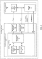
- FIG. 2 depicts a block diagram of a SOC 10.
- the SOC 10 includes a power management unit 12 and a digital processing unit 14.
- the power management unit 12 includes a digital control block 13 and (in this embodiment) two voltage regulators 16a and 16b, generating V memory and V logic , respectively.
- the digital control block 13 may generate more than two voltage values, and additional voltage regulators 16n may generate a corresponding number of supply voltages.
- the digital control block 13 includes a finite state machine 18, registers 20, and a regulator control block 22.
- the regulator control block 22 comprises hardware that implements a software-configurable dual power supply controller, under the control of the state machine 18, and relying on pre-programmed OPPs and other boundary condition data.
- data used by the regulator control block 22 may include OPP voltage values (or an offset to be added to another voltage to generate an OPP voltage value), constraints on the absolute voltage value or offset value of one or more voltages for various zones, and voltage values defining voltage zones.
- this data may be stored in registers 20 during an initialization phase, and accessed by the regulator control block 22 during an operational phase. In other embodiments, some of the data may be communicated to the regulator control block 22 dynamically during the operational phase, such as via a data communication bus.
- the digital processing unit 14 which may for example implement a digital baseband processor for a portable communication device, includes a digital core 28 and a memory array 26. By strictly controlling the boundary conditions between the digital core logic supply voltage V logic and the memory array supply voltage V memory , optimal performance may be achieved without requiring level shifters at every point of interface between the digital core 28 and the memory array 26.
- the digital core 28 controls the power management unit 12 by programming register 20 values via software, and by hardware control signals that transition the regulator control block 22 between predefined OPPs.
- the regulator control block 22 generates digital inputs to voltage regulators 16a and 16b that generate the V memory and V logic power supply voltages.
- the V memory power supply voltage is generated by applying a predetermined offset to the V logic power supply voltage. This ensures both that the offset does not violate any boundary conditions, and that V memory remains within the permissible absolute value range.
- the power management unit 12 operates, under the control of the digital core 28, to transition from one OPP to another. Accordingly, OPPs are predefined, and information about the OPPs is stored in registers 20 prior to operation.
- This information includes the V logic voltage of each OPP, the offset of V memory from V logic at that OPP, trigger point voltage values defining voltage zones, a plurality of minimum and maximum values for the offset between V logic and V memory per zone, and a plurality of absolute maximum and minimum permissible values for V logic and V memory per zone.
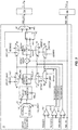
- Figure 3 depicts a detailed functional schematic diagram of the regulator control block 22. Schematic symbols of, e.g., comparators, multiplexors, and the like are functional indicators; the regulator control block 22 is digital.
- the logic_vsel data is generated conventionally - e.g., by a counter (not shown) - to set the V logic voltage level to a predetermined value for a selected OPP. This data is converted by voltage regulator 16b (which includes DAC functionality) into the V logic supply voltage provided to the digital logic 28.
- the regulator control block 22 simultaneously generates mem_vsel data to set the corresponding V memory voltage level for the selected OPP.
- the mem_vsel data is converted by voltage regulator 16a into the V memory supply voltage provided to the memory array 26.
- the digital core 28 indicates the selected new OPP to the power management unit 12, such as by encoding an OPP identification on an opp_sel[2:0] signal.
- the opp_sel[2:0] data will retrieve the target V logic value for the selected OPP, and ramp (not shown) the logic_vsel data from a current value to the target value to generate the target V logic voltage.
- the opp_sel[2:0] lines select by multiplexer M0, an OFFSETn from among a plurality of OFFSETs programmed into registers 20.
- an offset ramp generator 32 gradually ramps the mem_vsel data from its current value to the value indicated by the offset data retrieved from a register 20, over an appropriate duration (i.e., number of clock pulses).
- the OFFSETn value is then limited, in offset limiter block 34, to conform to boundary conditions.
- the boundary conditions may vary across the V logic /V memory voltage space. That is, an OPP with a relatively high value of V logic may allow a greater offset of V memory from the V logic value, than would be the case for an OPP with a relatively low value of V logic .
- the permissible maximum and minimum offset values thus depend on the value - or at least the neighborhood - of V logic .
- Trigger points separate the extent of permissible V logic values into zones, over which the boundary conditions are fairly close, and for which a maximum and minimum offset (and absolute V memory value) may be defined.
- three trigger points are defined, delineating four zones. The first and second trigger points control the minimum constraint values, and the third trigger point controls the maximum constraint values.
- TRIGGERPOINT1 As the logic-vsel value increases past the value of TRIGGER1, the output of comparator 42-1, or TRIGGERPOINT1, transitions to a 1; TRIGGERPOINT2 and TRIGGERPOINT3 remain 0. These signals are the select inputs to multiplexers M1-M6.
- the data inputs to the multiplexers M1-M6 are various pre-programmed maximum and minimum offset and absolute values (stored in registers 20), which constrain the generated V memory voltage. For example, as the logic_vsel value passes the first trigger point, the TRIGGERPOINTn outputs are ⁇ 1 0 0>, which select OFFSET_MIN2 and OFFSET_MAX1.
- the OFFSET value retrieved from registers 20 (and ramped up to its full value) is constrained to these minimum and maximum values at the offset limiter block 34.
- the constrained offset value is then added to the logic_vsel value at the adder 36 to generate a preliminary mem_vsel value.
- the preliminary mem_vsel value will increase as well, since the constrained offset value is added to logic_vsel to generate mem_vsel.
- mem_vsel violate the applicable boundary condition that its offset from logic_vsel be within predefined limits.
- the magnitude, or absolute, value of V memory is also limited, to be within pre-programmed minimum and maximum values for each trigger point-defined zone.
- the TRIGGERPOINTn signals of ⁇ 1 0 0> select ABSMIN2 and ABSMAX1.
- the output of the adder 36 is limited to be within these values at ABS limiter block 38, generating the final mem_vsel.
- This data are latched at flip-flop bank 40.
- the output of the flip-flop bank 40 if not bypassed at multiplexer M7, is the final mem_vsel value, which is the input to the voltage regulator 16a, which generates the V memory supply voltage provided to the memory array 26.
- Table 1 Constraint Values as a Function of Trigger Points TRIGGERPOINT COMPARATOR OUTPUTS 1-3 MINIMUM OFFSET MAXIMUM OFFSET MINIMUM ABSOLUTE MAXIMUM ABSOLUTE 000 OFFSET_MIN1 10 mV OFFSET_MAX1 90 mV ABSMIN1 0.95 V ABSMAX1 1.05 V 100 OFFSET_MIN2 -70 mV OFFSET_MAX1 90 mV ABSMIN2 1.00 V ABSMAX1 1.05 V 110 OFFSET_MIN2 -70 mV OFFSET_MAX2 -40 mV ABSMIN2 1.00 V ABSMAX2 1.15 V 111 OFFSET_MIN3 -100 mV OFFSET_MAX2 -40 mV ABSMIN3 1.07V ABSMAX2 1.15V
- Figure 4 depicts the operation of the power management unit 12 as the SOC 10 transitions between various representative OPPs. These OPPs are listed in Table 2. Table 2: Representative OPP Values OPP0 OPP1 OPP2 OPP5 V logic 1.17 V 1.04 V 0.94 V 1.19 V V memory offset -100 mV -20 mV 30 mV -50 mV
- the three trigger points defined for the SOC 10 divide the V logic voltage range into four zones. These trigger point voltages are as follows:
- ABSMIN2 1.00 V.
- V memory is constrained to 1.00 V.
- the applied offset of -20 mV is only applicable without constraint as V logic > 1.02V, along segment D. This offset is applied until OPP1 is reached.
- V logic increases while the offset ramps down from -20 mV to -100 mV, resulting in a flat, horizontal trajectory along segment E.
- V memory is constrained by the OFFSET_MIN2 limit of -70 mV, which is applied, along segment F, until V logic crosses TRIGGERPOINT3 at 1.14 V.
- ABSMIN3 1.07 V.
- V memory is maintained at this value, along segment G, until V logic reaches OPP0.
- the power management unit 12 is next commanded to move again to OPP1.
- V logic decreases while the offset ramps up from -50 mV to -20 mV, resulting in a flat horizontal line.
- the offset quickly hits the limit OFFSET_MAX2 of -40 mV, and is constrained to this value along segment K, until V logic passes TRIGGERPOINT2.
- the ABSMAX1 limit of 1.05 V applies, constraining V memory to this value along segment L, until the offset reaches its target value of -20 mV (due to V logic decreasing to 1.07 V).
- An unconstrained -20 mV offset is then applied along segment M, until reaching OPP1.
- the transitions between OPPs demonstrate voltage trajectories for a hypothetical SOC 10, as it transitions from a power-conserving mode (OPP2) through increased power demands to a high-performance mode (OPP5), and back, with different constraints applied in different voltage zones.
- the power management unit 12 may arbitrarily be commanded from any V logic /V memory voltage relationship point - either an OPP or a transition point between OPPs - to any OPP, and it is guaranteed to observe all boundary conditions (i.e., constraints on offset and V memory value for the relevant trigger point zone). This is because as V logic crosses a trigger point into a different zone, different limiting values may apply, and V memory will be constrained accordingly.
- Figure 4 demonstrates that arbitrarily complex rules and boundary conditions regarding the relative voltage values between two supply voltages, such as V logic and V memory , may be implemented with a few simple constraints on the offset value and absolute voltage values of the second voltage value, and by defining the zones where the different constraints apply by setting a few trigger points.
- those of skill in the art may easily set the OPPs, constraints, and trigger points based on the requirements of a particular SOC 10 or other circuit.
- the inventive concept may easily be extended to generate any number of dependent voltages as offsets from a primary voltage, each with the same or different constraints and trigger points.
- FIG. 5 depicts an alternative embodiment of the regulator control unit 22.
- a Pwrctrl[0:3] signal selects voltage levels for both V memory and V logic , at multiplexers 50a and 50b, respectively.
- the target V memory level may be selected directly, or a per-zone constrained value may be selected.
- Ramp circuits 52a, 52b gradually ramp the voltages V memory and V logic from current values to the selected values (although this feature may be bypassed for V memory by multiplexer 54).
- digital comparators 56-1, 56-2, and 56-3 compare V logic to predetermined voltage zone boundary values denoted Zone n_ low_limit. These comparators operate similarly to the trigger point comparators 42 of Figure 3 , to divide the V logic voltage range into two or more zones.
- the V logic /V memory graph inset in Figure 5 depicts these zones.
- Logic gates 58 decode the zone comparison outputs to generate selectors for Zone n _set_point multiplexers, which select the set point to provide to the ramp generator 52a, depending on the active zone. That set point, for each zone, may be an absolute value retrieved from registers 20, or an offset, also retrieved from registers 20, and applied to logic_vsel by adders 64. This selection between predetermined absolute value or offset to logic_vsel is determined, independently for each zone, by Absolute n /Offset n _sel signals.
- the graph in Figure 5 depicts three OPPs, depicted by + symbols.
- This graph depicts the case that offsets are selected by multiplexers 62 for zones 0 and 2, which are added to logic_vsel, and hence the voltage trajectory rises with a constant slope across these zones.
- Absolute values are selected for zones 1 and 3, which match the mem_vsel value at the end of the preceding zone, resulting in a flat, horizontal trajectory across these zones.
- voltage trajectories across zones are directly selected, as opposed to the embodiment of Figure 3 , which defines and enforces zone-specific limits for possible trajectories.
- the embodiment of Figure 5 is limited to one OPP per zone, which may be sufficient for many designs (or more zones may be defined).
- Figure 6 depicts a method 100 of controlling a plurality of supply voltages provided to one or more electronic circuits, wherein permissible values of at least first and second voltages of the plurality are constrained both absolutely and relative to each other.
- the range of permissible values for a first voltage is divided into two or more zones, and one or more trigger point voltage values delimiting the zones are stored to registers 20 (block 102).
- a plurality of operating performance points (OPP), each OPP specifying values for the first and second voltages and boundary conditions, are defined (block 104).
- the OPP values (in the case of the second voltage, either absolute voltage values or offsets, per zone) are also stored in registers 20.
- a target OPP is selected (block 106), such as by a digital core 28 of an SOC 10, and the selected OPP is communicated to the power management unit 12.
- Two actions then proceed in parallel.
- the first voltage value is gradually ramped from a current value to the OPP value for the first voltage (block 108).
- a target second voltage value within each zone is generated (block 110). This may occur two ways: either the target second voltage value is selected from a register (block 112), or a target offset value is selected from a register 20, and added to the first voltage value (block 114).
- a second voltage value is ramped from a current value to the generated target value for the current zone (block 116)
- the second voltage value is constrained, both in the voltage value and in the difference between the second voltage value and the first voltage value, wherein the constraints are unique to each zone (block 116).
- the operational process may be repeated by selecting a new target (predefined) OPP (block 106).
- Embodiments of the present invention present numerous advantages over the prior art. More optimal and power-efficient performance of SOC is possible, as greater freedom is provided in supplying different circuits (such as memory arrays and digital logic) with different supply voltages. Where a large number of level shifters is impractical and hence strict relationships between the relative levels of the voltages are imposed by circuit constraints, embodiments of the present invention guarantee that these relationships, or boundary conditions, are not violated at any time. This guarantee is independent of the speed or timing of software commands, and the guarantee holds thorough even unpredictable transitions, such as commanding a first OPP, and then commanding a second OPP mid-way through the transition to the first OPP.
- SOC may respond more quickly to changes in the operational environment, such as the instantaneous computational or communications demand.
- An arbitrarily complex set of constraints may be imposed by specifying relatively few parameters, and defining a few zones in which the different constraints apply.
Landscapes
- Engineering & Computer Science (AREA)
- Power Engineering (AREA)
- Theoretical Computer Science (AREA)
- Physics & Mathematics (AREA)
- General Engineering & Computer Science (AREA)
- General Physics & Mathematics (AREA)
- Power Sources (AREA)
Description
- The present invention relates generally to electronic circuits, and in particular to a system and method of dynamically controlling multiple voltage regulators to ensure strict relationships between the respective voltages at all times.
- Portable electronic devices are ubiquitous accoutrements in modern life. Cellular telephones, smartphones, satellite navigation receivers, e-book readers and tablet computers, wearable computers (e.g., glasses, wrist computing), cameras, and music players are just a few examples of the many types of portable electronic devices in widespread use. Portable electronic devices are powered by batteries - either replaceable batteries such as alkaline cells, or rechargeable batteries such as NiCd, NiMH, LiOn, or the like. In either case, the useful life of portable electronic devices is limited by available battery power, which decreases in proportion to the length of use of the device, and the level of power consumption during that use.
- Trends in portable electronic device design include higher levels of circuit integration, shrinking device form factors (and hence smaller batteries), increasing functionality, and wireless connectivity - all of which have made power management a critical area of optimization for portable electronic device designers.
- Power management is particularly critical for very highly integrated circuits. Processing circuits, associated logic circuits (DMA, graphics processing, encryption, RF baseband processing, etc.) and memory are often integrated into the same IC die (or separate dice that are packaged together). This is known in the art as "System On a Chip," or SOC. One approach to intelligent power management on SOC, which may include circuits having different power consumption profiles and operating frequencies, is to dynamically vary the clock frequency and voltage levels of power supplies during operation, in response to instantaneous demand (processing load, communications activity, and the like). This is known as Dynamic Voltage and Frequency Scaling (DVFS) or Dynamic Voltage Scaling (DVS). DVFS/DVS is routinely employed for battery-powered SOC, because maintaining voltage levels at the levels required for maximum operational performance will cause average battery power life to be significantly lower than when voltage levels are scaled dynamically along with the required performance. For example, for digital devices, supplying a
voltage level 10% higher than required results in at least 21% higher power consumption drawn from the battery. DVFS/DVS is also advantageous from the perspective of thermal management. - SOC typically have a power architecture with numerous power rails running inside the silicon die (with different requirements for voltage, current, and power sequence). The power rails in the SOC are typically supplied from analog mixed signal components, such as voltage regulators (also called as power supplies). The voltage regulator outputs typically have a built-in slew rate control, to protect the system from battery surge currents when the regulator output voltages are changed.
- There are usually some dependencies between power rails in the SOC due to the fact that two or more power supplies are fed to single components at many places of the die. For example, this is the case for level shifter components that are inserted when signals traverse from one power domain to another. The level shifter is then connected to the supplies of both power domains. However, in some situations there are speed constraints that preclude the use of a traditional level shifter. One such case, where special constraint between the power supplies can exist on a SOC, is the on-chip memory. The supply voltage for the memory array (called Vmemory) is ideally higher than the supply voltage for the digital interface (called Vlogic). This is because the noise instability is higher for memory cell than for logic cells, and this is generally true for any kind of CMOS process designs. However, inserting level shifters between the memory array and its interface logic may not be practical, due to the number of such connections, and/or performance constraints. Accordingly, the two circuits may be operated at different voltages. However, the memory array voltage supply must meet certain voltage boundary conditions in order for the memory to work at the required speed.
- For example, the voltage boundary conditions may be specified as:
- Vmemory - Vlogic < 350 mV, and
- Vlogic - Vmemory < 200 mV.
- If one of the Vmemory or Vlogic supply voltages is changed, then the other must change accordingly to ensure that the voltage boundary conditions are met at all times, in order to guarantee proper memory operation. Since DVFS/DVS is required for reasonable power consumption for SOC, changing two power supplies in a precise, rapid and linked way is necessary for the SOC device to work correctly, and power efficiently.
- One known SOC is a baseband processor for a wireless communication device. This chip includes both digital logic and on-chip memory, with the power supplies for both circuits tied together; a single voltage regulator supplies power for the entire chip. Because the memory array and digital logic voltages are tied together, the memory array cannot be operated at a higher voltage than the digital core logic. The allowed voltage range for digital core logic of the SOC is thus more narrow than otherwise possible, and hence the power consumption is higher than optimum.
- Another known SOC - a more sophisticated solution for a wireless communication device - is a two-chip solution tightly integrating a baseband processor and RF transceiver. In this SOC, the memory array power supply is a Low Drop Out (LDO) regulator, and the digital logic power supply is a switching DCDC power supply. In this case, Vmemory is fixed, and Vlogic may vary over an acceptable range without violating the voltage boundary conditions. While this solution improves performance, it still restricts Vlogic, which in some use cases must be higher than it could otherwise be, due to Vmemory being fixed.
- The simple solution of making both Vmemory and Vlogic independently variable is problematic. First, there can be unspecified delays between the commands that control Vmemory and those that control Vlogic. This can result in the voltage boundary conditions to be broken temporarily. Second, the voltages may have different ramp times, making it complicated to adjust the delay between two commands. Third, since the voltage changes are driven by operating conditions, there can be a sudden need to achieve a new operation point while the transition to a previous one is still in progress, resulting voltage trajectories that are difficult to predict, and which hence may violate boundary conditions.
- The changes to Vmemory and Vlogic could be broken into numerous small steps, and the incremental changes interleaved between the two voltage supplies. This would make it possible to adjust the voltages without violating boundary conditions. However, it would introduce significant delay, resulting in increased power consumption. In some cases, such an approach may fail to achieve required supply levels quickly enough to meet operational demands.
-
US 2012/0023345 describes a method of managing current and power in a computer system by allocating power credits to computational units across a die. -
US 5,946,242 shows a circuit for generating an internal source voltage signal responsive to an external source voltage signal. The internal source voltage signal may be lower in a stress operating mode. - The Background section of this document is provided to place embodiments of the present invention in technological and operational context, to assist those of skill in the art in understanding their scope and utility. Unless explicitly identified as such, no statement herein is admitted to be prior art merely by its inclusion in the Background section.
- The following presents a simplified summary of the disclosure in order to provide a basic understanding to those of skill in the art. This summary is not an extensive overview of the disclosure and is not intended to identify key/critical elements of embodiments of the invention or to delineate the scope of the invention. The sole purpose of this summary is to present some concepts disclosed herein in a simplified form as a prelude to the more detailed description that is presented later.
- The present invention is defined by the appended independent claims. Further aspects of the invention are outlined in the dependent claims. Embodiments which do not fall within the scope of the claims do not form part of the present invention.
- According to one or more embodiments described and claimed herein, a power control system provides multiple supply voltages that are guaranteed not to violate boundary conditions regardless of the timing of voltage change commands. The invention is presented in the context of two power supply voltages; however, it may easily be extended to multiple outputs. A first voltage (Vlogic in the embodiments described herein) is controlled conventionally, and a second voltage (Vmemory) is either selected, or generated by adding a selected offset to the first voltage. Both the size of the offset, and the absolute value of the second voltage, are constrained at all times, by constraint values specific to the current voltage zone. The invention ensures a smooth transition between different voltage operating points, and ensures that the trajectory of change between specified operating points remains within predefined boundaries.
- The present invention will now be described more fully hereinafter with reference to the accompanying drawings, in which embodiments of the invention are shown. However, this invention should not be construed as limited to the embodiments set forth herein. Rather, these embodiments are provided so that this disclosure will be thorough and complete, and will fully convey the scope of the invention to those skilled in the art. Like numbers refer to like elements throughout.
-
Figure 1 is a graph of absolute and relative constraints of and between two supply voltages. -
Figure 2 is a functional block diagram of a System on a Chip. -
Figure 3 is a functional schematic diagram of a first embodiment of the regulator control circuit ofFig. 2 . -
Figure 4 is a graph of two supply voltages and transitions between operating performance points. -
Figure 5 is a functional schematic diagram of a second embodiment of the regulator control circuit ofFig. 2 . -
Figure 6 is a flow diagram of a method of controlling a plurality of supply voltages. - It should be understood at the outset that although illustrative implementations of one or more embodiments of the present disclosure are provided below, the disclosed systems and/or methods may be implemented using any number of techniques, whether currently known or not yet in existence. The disclosure should in no way be limited to the illustrative implementations, drawings, and techniques illustrated below, including the exemplary designs and implementations illustrated and described herein, but may be modified within the scope of the appended claims.
-
Figure 1 depicts a graph of the relationship between a first power supply voltage applied to digital logic circuits (Vlogic) and a second power supply voltage applied to a memory array (Vmemory).Figure 1 depicts, in the dotted area, absolute voltage values that are impermissible - neither Vlogic nor Vmemory may extend into these regions. The graph also depicts, in positive-slope hashing, regions within the allowed maximum range, but which represent an impermissible combination - that is, a combination of Vlogic and Vmemory that violates one or more boundary conditions. The negative-slope hashed area ofFigure 1 represents values of Vlogic and Vmemory that are legal combinations. Any point within this area may be selected as an Operating Performance Point (OPP). - An OPP is a pre-defined Vlogic - Vmemory relationship point, where appropriate voltage levels are specified for low power consumption, high performance, or some compromise between these goals. OPPs are programmed in software or a hardware state machine and transitions between them are implemented by a system controller. If the system controller decides to move from one OPP to another OPP, the consequence is a voltage adjustment path (trajectory), which shows the voltage level relationship at particular voltage levels. Since the SOC is operating during the voltage level transitions, it is critical that the voltage trajectory between OPPs remain within the negative-sloped hashed area.
- It is possible for software to pre-program the various OPP control parameters, and configure the system controller to change OPPs upon a change in the state of hardware control signals. This method is advantageous in terms of speed.
-
Figure 2 depicts a block diagram of aSOC 10. TheSOC 10 includes apower management unit 12 and adigital processing unit 14. Thepower management unit 12 includes adigital control block 13 and (in this embodiment) twovoltage regulators digital control block 13 may generate more than two voltage values, and additional voltage regulators 16n may generate a corresponding number of supply voltages. Thedigital control block 13 includes afinite state machine 18, registers 20, and aregulator control block 22. Theregulator control block 22 comprises hardware that implements a software-configurable dual power supply controller, under the control of thestate machine 18, and relying on pre-programmed OPPs and other boundary condition data. In various embodiments, as described in greater detail herein, data used by theregulator control block 22 may include OPP voltage values (or an offset to be added to another voltage to generate an OPP voltage value), constraints on the absolute voltage value or offset value of one or more voltages for various zones, and voltage values defining voltage zones. In some embodiments, this data may be stored inregisters 20 during an initialization phase, and accessed by theregulator control block 22 during an operational phase. In other embodiments, some of the data may be communicated to theregulator control block 22 dynamically during the operational phase, such as via a data communication bus. - The
digital processing unit 14, which may for example implement a digital baseband processor for a portable communication device, includes adigital core 28 and amemory array 26. By strictly controlling the boundary conditions between the digital core logic supply voltage Vlogic and the memory array supply voltage Vmemory, optimal performance may be achieved without requiring level shifters at every point of interface between thedigital core 28 and thememory array 26. Thedigital core 28 controls thepower management unit 12 by programmingregister 20 values via software, and by hardware control signals that transition theregulator control block 22 between predefined OPPs. - The
regulator control block 22 generates digital inputs tovoltage regulators power management unit 12 operates, under the control of thedigital core 28, to transition from one OPP to another. Accordingly, OPPs are predefined, and information about the OPPs is stored inregisters 20 prior to operation. This information includes the Vlogic voltage of each OPP, the offset of Vmemory from Vlogic at that OPP, trigger point voltage values defining voltage zones, a plurality of minimum and maximum values for the offset between Vlogic and Vmemory per zone, and a plurality of absolute maximum and minimum permissible values for Vlogic and Vmemory per zone. -
Figure 3 depicts a detailed functional schematic diagram of theregulator control block 22. Schematic symbols of, e.g., comparators, multiplexors, and the like are functional indicators; theregulator control block 22 is digital. The logic_vsel data is generated conventionally - e.g., by a counter (not shown) - to set the Vlogic voltage level to a predetermined value for a selected OPP. This data is converted byvoltage regulator 16b (which includes DAC functionality) into the Vlogic supply voltage provided to thedigital logic 28. Theregulator control block 22 simultaneously generates mem_vsel data to set the corresponding Vmemory voltage level for the selected OPP. The mem_vsel data is converted byvoltage regulator 16a into the Vmemory supply voltage provided to thememory array 26. - Operation of the
regulator control block 22 is best explained in the context of a transition from a first OPP to a second OPP. Thedigital core 28 indicates the selected new OPP to thepower management unit 12, such as by encoding an OPP identification on an opp_sel[2:0] signal. The opp_sel[2:0] data will retrieve the target Vlogic value for the selected OPP, and ramp (not shown) the logic_vsel data from a current value to the target value to generate the target Vlogic voltage. Simultaneously, the opp_sel[2:0] lines select by multiplexer M0, an OFFSETn from among a plurality of OFFSETs programmed into registers 20. - To prevent sudden changes in the memory array supply voltage Vmemory, which may cause deleterious effects such as supply rail ringing, current inrush, or the like, an offset
ramp generator 32 gradually ramps the mem_vsel data from its current value to the value indicated by the offset data retrieved from aregister 20, over an appropriate duration (i.e., number of clock pulses). - The OFFSETn value is then limited, in offset
limiter block 34, to conform to boundary conditions. In general, the boundary conditions may vary across the Vlogic/Vmemory voltage space. That is, an OPP with a relatively high value of Vlogic may allow a greater offset of Vmemory from the Vlogic value, than would be the case for an OPP with a relatively low value of Vlogic. The permissible maximum and minimum offset values thus depend on the value - or at least the neighborhood - of Vlogic. - To select the proper maximum and minimum offset values, a plurality of trigger points is defined, and programmed into
registers 20 prior to use. Trigger points separate the extent of permissible Vlogic values into zones, over which the boundary conditions are fairly close, and for which a maximum and minimum offset (and absolute Vmemory value) may be defined. In this embodiment, three trigger points are defined, delineating four zones. The first and second trigger points control the minimum constraint values, and the third trigger point controls the maximum constraint values. - Assume the
SOC 10 has been operating at an OPP with low voltage values for Vlogic and Vmemory (i.e., below all trigger points). An increased computational load prompts thedigital core 28 to specify a higher-voltage OPP. The logic_vsel data value increases, and the OFFSETn value corresponding to the selected OPP is retrieved and ramped up by theramp generator 32. The logic_vsel value is compared to (in this embodiment) three TRIGGER values (stored in registers 20) at comparators 42-1, 42-2, and 42-3. As the logic-vsel value increases past the value of TRIGGER1, the output of comparator 42-1, or TRIGGERPOINT1, transitions to a 1; TRIGGERPOINT2 and TRIGGERPOINT3 remain 0. These signals are the select inputs to multiplexers M1-M6. The data inputs to the multiplexers M1-M6 are various pre-programmed maximum and minimum offset and absolute values (stored in registers 20), which constrain the generated Vmemory voltage. For example, as the logic_vsel value passes the first trigger point, the TRIGGERPOINTn outputs are <1 0 0>, which select OFFSET_MIN2 and OFFSET_MAX1. - The OFFSET value retrieved from registers 20 (and ramped up to its full value) is constrained to these minimum and maximum values at the offset
limiter block 34. The constrained offset value is then added to the logic_vsel value at theadder 36 to generate a preliminary mem_vsel value. As the logic_vsel value increases, on the way to the selected OPP, the preliminary mem_vsel value will increase as well, since the constrained offset value is added to logic_vsel to generate mem_vsel. However, at no point will mem_vsel violate the applicable boundary condition that its offset from logic_vsel be within predefined limits. - In a manner similar to the limiting of the offset, the magnitude, or absolute, value of Vmemory is also limited, to be within pre-programmed minimum and maximum values for each trigger point-defined zone. The TRIGGERPOINTn signals of <1 0 0> select ABSMIN2 and ABSMAX1. The output of the
adder 36 is limited to be within these values atABS limiter block 38, generating the final mem_vsel. This data are latched at flip-flop bank 40. The output of the flip-flop bank 40, if not bypassed at multiplexer M7, is the final mem_vsel value, which is the input to thevoltage regulator 16a, which generates the Vmemory supply voltage provided to thememory array 26. Inspection ofFigure 3 yields the following table of constraints applied to the generated offset voltage, along with representative values applicable to an example presented inFigure 4 .Table 1: Constraint Values as a Function of Trigger Points TRIGGERPOINT COMPARATOR OUTPUTS 1-3 MINIMUM OFFSET MAXIMUM OFFSET MINIMUM ABSOLUTE MAXIMUM ABSOLUTE 000 OFFSET_MIN1 10 mV OFFSET_MAX1 90 mV ABSMIN1 0.95 V ABSMAX1 1.05 V 100 OFFSET_MIN2 - 70 mV OFFSET_MAX1 90 mV ABSMIN2 1.00 V ABSMAX1 1.05 V 110 OFFSET_MIN2 -70 mV OFFSET_MAX2 -40 mV ABSMIN2 1.00 V ABSMAX2 1.15 V 111 OFFSET_MIN3 -100 mV OFFSET_MAX2 -40 mV ABSMIN3 1.07V ABSMAX2 1.15V -
Figure 4 depicts the operation of thepower management unit 12 as theSOC 10 transitions between various representative OPPs. These OPPs are listed in Table 2.Table 2: Representative OPP Values OPP0 OPP1 OPP2 OPP5 Vlogic 1.17 V 1.04 V 0.94 V 1.19 V Vmemory offset -100 mV -20 mV 30 mV -50 mV - The three trigger points defined for the
SOC 10 divide the Vlogic voltage range into four zones. These trigger point voltages are as follows: - TRIGGERPOINT1 = 0.99 V
- TRIGGERPOINT2 = 1.09 V
- TRIGGERPOINT2 = 1.14 V
- Referring to
Figure 4 , assume theSOC 10 is initially operating at OPP2, below TRIGGERPOINT1, and thedigital core 28 issues a command to move to OPP1. The initial voltage trajectory is a flat, horizontal line from Vlogic = 0.94 V to 0.96 V, because the Vlogic voltage is rising while the offset is ramping down from +30 mV to -20 mV. This segment is indicated inFigure 4 by the label A. At the point Vlogic = 0.96 V, the offset is +10 mV, and is limited by the OFFSET_MIN1 limit value - the offset cannot fall below that value in this zone. The Vmemory value then follows the increase in Vlogic, with a +10mV offset, along the trajectory segment labeled B, until TRIGGERPOINT1 is reached at Vlogic = 0.99 V. Note that without OFFSET_MIN1 limiting the Vmemory value, the voltage trajectory would be straight line until Vlogic = 0.99 V and the Vmemory would assume impermissible values. - As Vlogic crosses TRIGGERPOINT1 at 0.99 V, the OFFSET_MIN1 limit no longer applies. However, Vmemory is in this zone constrained by ABSMIN2 = 1.00 V. Hence, along segment C, as Vlogic increases to 1.02 V, Vmemory is constrained to 1.00 V. The applied offset of -20 mV is only applicable without constraint as Vlogic > 1.02V, along segment D. This offset is applied until OPP1 is reached.
- If the
power management unit 12 is then commanded to move to OPP0, a similar trajectory results. Vlogic increases while the offset ramps down from -20 mV to -100 mV, resulting in a flat, horizontal trajectory along segment E. As Vlogic crosses TRIGGERPOINT2 at 1.09 V, Vmemory is constrained by the OFFSET_MIN2 limit of -70 mV, which is applied, along segment F, until Vlogic crosses TRIGGERPOINT3 at 1.14 V. In this zone, the absolute minimum permissible value of Vmemory is ABSMIN3 = 1.07 V. Vmemory is maintained at this value, along segment G, until Vlogic reaches OPP0. - If the
power management unit 12 is then commanded to move to OPP5, a very steep climb in the trajectory occurs along segment H, due to both Vlogic increasing, and the offset ramping up from -100 mV to -50 mV. After Vlogic reaches its OPP5 value of 1.19 V, the offset continues to increase, causing a vertical trajectory along segment I, until the offset reaches -50 mV, yielding Vmemory = 1.14V at OPP5. Note that the trajectory from OPP0 to OPP5 was unconstrained, either in the offset or the absolute voltage value of Vmemory. - Continuing the example, the
power management unit 12 is next commanded to move again to OPP1. Initially, along segment J, Vlogic decreases while the offset ramps up from -50 mV to -20 mV, resulting in a flat horizontal line. However, the offset quickly hits the limit OFFSET_MAX2 of -40 mV, and is constrained to this value along segment K, until Vlogic passes TRIGGERPOINT2. In this region, the ABSMAX1 limit of 1.05 V applies, constraining Vmemory to this value along segment L, until the offset reaches its target value of -20 mV (due to Vlogic decreasing to 1.07 V). An unconstrained -20 mV offset is then applied along segment M, until reaching OPP1. - In moving from OPP1 to OPP2, the offset ramps up from -20 mV to +30 mV, while Vlogic decreases, resulting in a flat, horizontal trajectory along segment N. At Vlogic = 0.99 V, the target offset of +30 mV is reached, and is maintained as Vlogic decreases, along segment O, to OPP2. Note that the change in trajectory between segments N and O coincided with crossing TRIGGERPOINT1; however, the corresponding change in offset and absolute constraints did not affect the trajectory in this example.
- The transitions between OPPs, described with reference to
Figure 4 , demonstrate voltage trajectories for ahypothetical SOC 10, as it transitions from a power-conserving mode (OPP2) through increased power demands to a high-performance mode (OPP5), and back, with different constraints applied in different voltage zones. However, thepower management unit 12 according to embodiments of the present invention also may arbitrarily be commanded from any Vlogic/Vmemory voltage relationship point - either an OPP or a transition point between OPPs - to any OPP, and it is guaranteed to observe all boundary conditions (i.e., constraints on offset and Vmemory value for the relevant trigger point zone). This is because as Vlogic crosses a trigger point into a different zone, different limiting values may apply, and Vmemory will be constrained accordingly. -
Figure 4 demonstrates that arbitrarily complex rules and boundary conditions regarding the relative voltage values between two supply voltages, such as Vlogic and Vmemory, may be implemented with a few simple constraints on the offset value and absolute voltage values of the second voltage value, and by defining the zones where the different constraints apply by setting a few trigger points. In any implementation, those of skill in the art may easily set the OPPs, constraints, and trigger points based on the requirements of aparticular SOC 10 or other circuit. Furthermore, the inventive concept may easily be extended to generate any number of dependent voltages as offsets from a primary voltage, each with the same or different constraints and trigger points. -
Figure 5 depicts an alternative embodiment of theregulator control unit 22. A Pwrctrl[0:3] signal selects voltage levels for both Vmemory and Vlogic, atmultiplexers multiplexer 51, the target Vmemory level may be selected directly, or a per-zone constrained value may be selected.Ramp circuits - In the mode that Vmemory is constrained in each zone, digital comparators 56-1, 56-2, and 56-3 compare Vlogic to predetermined voltage zone boundary values denoted Zonen_low_limit. These comparators operate similarly to the trigger point comparators 42 of
Figure 3 , to divide the Vlogic voltage range into two or more zones. The Vlogic/Vmemory graph inset inFigure 5 depicts these zones.Logic gates 58 decode the zone comparison outputs to generate selectors for Zonen_set_point multiplexers, which select the set point to provide to theramp generator 52a, depending on the active zone. That set point, for each zone, may be an absolute value retrieved fromregisters 20, or an offset, also retrieved fromregisters 20, and applied to logic_vsel byadders 64. This selection between predetermined absolute value or offset to logic_vsel is determined, independently for each zone, by Absoluten/Offsetn_sel signals. - The graph in
Figure 5 depicts three OPPs, depicted by + symbols. This graph depicts the case that offsets are selected bymultiplexers 62 forzones zones Figure 3 , which defines and enforces zone-specific limits for possible trajectories. Also, the embodiment ofFigure 5 is limited to one OPP per zone, which may be sufficient for many designs (or more zones may be defined). -
Figure 6 depicts amethod 100 of controlling a plurality of supply voltages provided to one or more electronic circuits, wherein permissible values of at least first and second voltages of the plurality are constrained both absolutely and relative to each other. In an initialization phase, above a dashed line inFigure 6 , the range of permissible values for a first voltage is divided into two or more zones, and one or more trigger point voltage values delimiting the zones are stored to registers 20 (block 102). A plurality of operating performance points (OPP), each OPP specifying values for the first and second voltages and boundary conditions, are defined (block 104). The OPP values (in the case of the second voltage, either absolute voltage values or offsets, per zone) are also stored inregisters 20. - In an operational phase, below the dashed line, a target OPP is selected (block 106), such as by a
digital core 28 of anSOC 10, and the selected OPP is communicated to thepower management unit 12. Two actions then proceed in parallel. First, the first voltage value is gradually ramped from a current value to the OPP value for the first voltage (block 108). Second, a target second voltage value within each zone is generated (block 110). This may occur two ways: either the target second voltage value is selected from a register (block 112), or a target offset value is selected from aregister 20, and added to the first voltage value (block 114). However the target second voltage is generated, a second voltage value is ramped from a current value to the generated target value for the current zone (block 116) The second voltage value is constrained, both in the voltage value and in the difference between the second voltage value and the first voltage value, wherein the constraints are unique to each zone (block 116). The operational process may be repeated by selecting a new target (predefined) OPP (block 106). - Embodiments of the present invention present numerous advantages over the prior art. More optimal and power-efficient performance of SOC is possible, as greater freedom is provided in supplying different circuits (such as memory arrays and digital logic) with different supply voltages. Where a large number of level shifters is impractical and hence strict relationships between the relative levels of the voltages are imposed by circuit constraints, embodiments of the present invention guarantee that these relationships, or boundary conditions, are not violated at any time. This guarantee is independent of the speed or timing of software commands, and the guarantee holds thorough even unpredictable transitions, such as commanding a first OPP, and then commanding a second OPP mid-way through the transition to the first OPP. Due to this ability to change OPP trajectory quickly while still observing all boundary conditions, SOC may respond more quickly to changes in the operational environment, such as the instantaneous computational or communications demand. An arbitrarily complex set of constraints may be imposed by specifying relatively few parameters, and defining a few zones in which the different constraints apply.
- The present invention may, of course, be carried out in other ways than those specifically set forth herein without departing from essential characteristics of the invention. The present embodiments are to be considered in all respects as illustrative and not restrictive, and all changes coming within the meaning of the appended claims are intended to be embraced therein.
Claims (8)
- A power management unit (12), comprising:a digital control circuit (13) operative to generate first and second voltage values (logic_vsel, mem_vsel) that are configured to gradually ramp during a transition from a first Operating Performance Point "OPP" to a second OPP, each OPP specifying target values for corresponding first and second supply voltages (Vlogic, Vmemory), in response to a selection of the second OPP communicated to the power management unit (12) ; andfirst and second voltage regulators (16a, 16b) operative to convert the first and second voltage values (logic_vsel, mem_vsel) to the first and second supply voltages (Vlogic, Vmemory) having corresponding voltage levels;wherein the digital control circuit (13) comprises:a plurality of registers (20) storing at least one trigger point voltage value (TRIGGER1-3), the trigger points dividing a permissible range of values of the first supply voltage (Vlogic) into two or more zones and OPP target values for the first and second supply voltages (Vlogic, Vmemory) for each selectable OPP; anda regulator control circuit (22) operative to generate the first and second voltage values (logic_vsel, mem_vsel) according to the OPP target values for the first OPP and the second OPP read from the registers, whereby the second voltage value (mem_vsel) is constrained, both in the voltage value and in the difference between the second voltage value (mem_vsel) and the first voltage value (logic_vsel), the constraints being unique to each zone.
- The power management unit of claim 1 wherein the regulator control circuit (22) comprises a plurality of digital comparators (42-1, 42-2, and 42-3) operative to compare the first voltage value (logic_vsel) with the one or more corresponding trigger point voltage values (TRIGGER1-3), to define the plurality of zones.
- The power management unit of claim 2 wherein the output of the digital comparators (42-1, 42-2, and 42-3) constrain the value corresponding to the second supply voltage (Vmemory) within each zone by selecting a target second voltage value for the current zone from a plurality of target second voltage values.
- A portable electronic device comprising the power management unit (12) of any of claims 1-3.
- A digital control circuit (13) for supplying at least first and second voltage values (logic_vsel, mem_vsel) to respective first and second voltage regulators (16a, 16b) operative to convert the respective first and second voltage values (logic_vsel, mem_vsel) to first and second supply voltages (Vlogic, Vmemory) wherein the first and second voltage values (logic_vsel, mem_vsel) are configured to gradually ramp during a transition from a first Operating Performance Point "OPP" to a selected second OPP, each OPP specifying a target value for the corresponding first supply voltage (Vlogic) and an offset of the corresponding second supply voltage (Vmemory) from the first supply voltage;
wherein the digital control circuit (13) comprises:a plurality of registers (20) for storing:a plurality of target offset values (OFFSET0-7), each offset value representing a difference between the first and second voltage values (logic_vsel, mem_vsel) for a corresponding OPP,at least one trigger point value (TRIGGER 1-3), the trigger point values dividing a permissible range of values of the first voltage value (logic_vsel) into a plurality of zones, anda plurality of offset limits (OFFSET_MIN1-3, OFFSET_MAX1-2) defining minimum and maximum differences between the first and second voltage values (logic_vsel, mem_vsel) for each zone; anda regulator control circuit (22) operative to receive the first voltage value (logic_vsel) and to generate the second voltage value (mem_vsel) during the transistion dependent on the values stored in the plurality of registers (20) such that the second voltage value (mem_vsel) is constrained both in the voltage value and in the difference between the second and first voltage values (logic_vsel, mem_vsel), the constraints being unique to each zone. - The digital control circuit of claim 5 wherein the plurality of registers (20) are further arranged to store maximum and minimum second voltage values (mem_vsel) for each zone.
- The digital control circuit of claim 5 or 6 further comprising:
at least one digital comparator (42-1 - 42-3) operative to compare the first voltage value (logic_vsel) with a corresponding trigger point value (TRIGGER 1-3). - The digital control circuit of any of claims 5-7 further comprising a finite state machine (18).
Applications Claiming Priority (2)
| Application Number | Priority Date | Filing Date | Title |
|---|---|---|---|
| US14/472,792 US10396553B2 (en) | 2014-08-29 | 2014-08-29 | System and method for control of multiple voltage regulators |
| PCT/EP2015/065015 WO2016030054A1 (en) | 2014-08-29 | 2015-07-01 | System and method for control of multiple voltage regulators |
Publications (2)
| Publication Number | Publication Date |
|---|---|
| EP3186691A1 EP3186691A1 (en) | 2017-07-05 |
| EP3186691B1 true EP3186691B1 (en) | 2020-03-25 |
Family
ID=53682648
Family Applications (1)
| Application Number | Title | Priority Date | Filing Date |
|---|---|---|---|
| EP15739195.4A Active EP3186691B1 (en) | 2014-08-29 | 2015-07-01 | System and method for control of multiple voltage regulators |
Country Status (4)
| Country | Link |
|---|---|
| US (2) | US10396553B2 (en) |
| EP (1) | EP3186691B1 (en) |
| ES (1) | ES2797053T3 (en) |
| WO (1) | WO2016030054A1 (en) |
Families Citing this family (2)
| Publication number | Priority date | Publication date | Assignee | Title |
|---|---|---|---|---|
| US10684671B2 (en) * | 2016-05-27 | 2020-06-16 | Qualcomm Incorporated | Adaptively controlling drive strength of multiplexed power from supply power rails in a power multiplexing system to a powered circuit |
| US11271566B2 (en) * | 2018-12-14 | 2022-03-08 | Integrated Device Technology, Inc. | Digital logic compatible inputs in compound semiconductor circuits |
Family Cites Families (13)
| Publication number | Priority date | Publication date | Assignee | Title |
|---|---|---|---|---|
| KR100200926B1 (en) * | 1996-08-29 | 1999-06-15 | 윤종용 | Internal power supply voltage generating circuit |
| US6700359B2 (en) | 2001-09-12 | 2004-03-02 | Texas Instruments Incorporated | Method for simultaneous output ramp up of multiple regulators |
| US7698583B2 (en) * | 2002-10-03 | 2010-04-13 | Via Technologies, Inc. | Microprocessor capable of dynamically reducing its power consumption in response to varying operating temperature |
| US7583555B2 (en) * | 2003-04-11 | 2009-09-01 | Qualcomm Incorporated | Robust and Efficient dynamic voltage scaling for portable devices |
| US7802113B2 (en) * | 2005-12-13 | 2010-09-21 | Silicon Laboratories Inc. | MCU with on-chip boost converter controller |
| US7925910B2 (en) * | 2007-07-19 | 2011-04-12 | Micron Technology, Inc. | Systems, methods and devices for limiting current consumption upon power-up |
| JP5577829B2 (en) * | 2010-05-07 | 2014-08-27 | 富士通セミコンダクター株式会社 | Power supply device, control circuit, and control method for power supply device |
| US8510582B2 (en) * | 2010-07-21 | 2013-08-13 | Advanced Micro Devices, Inc. | Managing current and power in a computing system |
| US9665144B2 (en) * | 2011-12-21 | 2017-05-30 | Intel Corporation | Methods and systems for energy efficiency and energy conservation including entry and exit latency reduction for low power states |
| US20130311792A1 (en) * | 2012-05-18 | 2013-11-21 | Prahallada PONNATHOTA | Voltage scaling architecture on system-on-chip platform |
| US9647453B2 (en) * | 2013-08-02 | 2017-05-09 | Samsung Electronics Co., Ltd. | Dual supply memory |
| US9577519B2 (en) * | 2014-02-05 | 2017-02-21 | Fairchild Semiconductor Corporation | Enhanced peak current mode DC-DC power converter |
| KR102190453B1 (en) * | 2014-02-17 | 2020-12-11 | 삼성전자주식회사 | Power management device and system on chip including the same |
-
2014
- 2014-08-29 US US14/472,792 patent/US10396553B2/en active Active
-
2015
- 2015-07-01 WO PCT/EP2015/065015 patent/WO2016030054A1/en not_active Ceased
- 2015-07-01 EP EP15739195.4A patent/EP3186691B1/en active Active
- 2015-07-01 ES ES15739195T patent/ES2797053T3/en active Active
-
2019
- 2019-07-18 US US16/515,301 patent/US10992132B2/en active Active
Non-Patent Citations (1)
| Title |
|---|
| None * |
Also Published As
| Publication number | Publication date |
|---|---|
| WO2016030054A1 (en) | 2016-03-03 |
| ES2797053T3 (en) | 2020-12-01 |
| US10396553B2 (en) | 2019-08-27 |
| US20160064928A1 (en) | 2016-03-03 |
| US20190341778A1 (en) | 2019-11-07 |
| US10992132B2 (en) | 2021-04-27 |
| EP3186691A1 (en) | 2017-07-05 |
Similar Documents
| Publication | Publication Date | Title |
|---|---|---|
| CN106873696B (en) | A kind of adaptive fast source voltage regulating system | |
| US8395440B2 (en) | Apparatus and method for controlling power gating in an integrated circuit | |
| US9990022B2 (en) | Adaptive power multiplexing with a power distribution network | |
| US9852859B2 (en) | Adjustable power rail multiplexing | |
| KR20150130500A (en) | Digitally assisted regulation for an integrated capless low-dropout(ldo) voltage regulator | |
| US20150036446A1 (en) | Dual supply memory | |
| US20190377405A1 (en) | Input Voltage Protection | |
| US10078358B2 (en) | System and method for reducing power delivery network complexity through local power multiplexers | |
| CN104076863B (en) | A kind of clock switching device | |
| WO2012104673A1 (en) | Integrated circuit device, voltage regulation circuitry and method for regulating a voltage supply signal | |
| EP1769314B1 (en) | Closed-loop control for performance tuning | |
| KR20170069269A (en) | Novel low cost, low power high performance smp/asmp multiple-processor system | |
| US11068006B2 (en) | Apparatus and method for power management with a two-loop architecture | |
| US10992132B2 (en) | System and method for control of multiple voltage regulators | |
| US20260003387A1 (en) | Controlled Transition Between Configuration Mode and User to Reduce Current-Resistance Voltage Drop | |
| US20190391608A1 (en) | Power multiplexer system for current load migration | |
| US10866608B2 (en) | Apparatus and method of voltage regulation control for integrated circuit | |
| US20150220128A1 (en) | Method and Apparatus for Use in a Data Processing System | |
| US20120072740A1 (en) | Power Booting Sequence Control System and Control Method Thereof | |
| JP2008507117A (en) | Control method for binary control of performance parameters | |
| US20130043936A1 (en) | Method And Apparatus For Controlling Power Supply | |
| EP2795423B1 (en) | Apparatus and method for managing power in a computing system | |
| US10203743B2 (en) | Reference voltage circuits in microcontroller systems | |
| US12339729B2 (en) | General purpose input/output (GPIO) supply harvesting | |
| US20240329707A1 (en) | Power management for multiple circuit domains |
Legal Events
| Date | Code | Title | Description |
|---|---|---|---|
| STAA | Information on the status of an ep patent application or granted ep patent |
Free format text: STATUS: THE INTERNATIONAL PUBLICATION HAS BEEN MADE |
|
| PUAI | Public reference made under article 153(3) epc to a published international application that has entered the european phase |
Free format text: ORIGINAL CODE: 0009012 |
|
| STAA | Information on the status of an ep patent application or granted ep patent |
Free format text: STATUS: REQUEST FOR EXAMINATION WAS MADE |
|
| 17P | Request for examination filed |
Effective date: 20170314 |
|
| AK | Designated contracting states |
Kind code of ref document: A1 Designated state(s): AL AT BE BG CH CY CZ DE DK EE ES FI FR GB GR HR HU IE IS IT LI LT LU LV MC MK MT NL NO PL PT RO RS SE SI SK SM TR |
|
| AX | Request for extension of the european patent |
Extension state: BA ME |
|
| DAV | Request for validation of the european patent (deleted) | ||
| DAX | Request for extension of the european patent (deleted) | ||
| STAA | Information on the status of an ep patent application or granted ep patent |
Free format text: STATUS: EXAMINATION IS IN PROGRESS |
|
| 17Q | First examination report despatched |
Effective date: 20190103 |
|
| GRAP | Despatch of communication of intention to grant a patent |
Free format text: ORIGINAL CODE: EPIDOSNIGR1 |
|
| STAA | Information on the status of an ep patent application or granted ep patent |
Free format text: STATUS: GRANT OF PATENT IS INTENDED |
|
| INTG | Intention to grant announced |
Effective date: 20190926 |
|
| GRAJ | Information related to disapproval of communication of intention to grant by the applicant or resumption of examination proceedings by the epo deleted |
Free format text: ORIGINAL CODE: EPIDOSDIGR1 |
|
| STAA | Information on the status of an ep patent application or granted ep patent |
Free format text: STATUS: EXAMINATION IS IN PROGRESS |
|
| GRAS | Grant fee paid |
Free format text: ORIGINAL CODE: EPIDOSNIGR3 |
|
| STAA | Information on the status of an ep patent application or granted ep patent |
Free format text: STATUS: GRANT OF PATENT IS INTENDED |
|
| GRAP | Despatch of communication of intention to grant a patent |
Free format text: ORIGINAL CODE: EPIDOSNIGR1 |
|
| GRAA | (expected) grant |
Free format text: ORIGINAL CODE: 0009210 |
|
| STAA | Information on the status of an ep patent application or granted ep patent |
Free format text: STATUS: THE PATENT HAS BEEN GRANTED |
|
| INTC | Intention to grant announced (deleted) | ||
| INTG | Intention to grant announced |
Effective date: 20200211 |
|
| AK | Designated contracting states |
Kind code of ref document: B1 Designated state(s): AL AT BE BG CH CY CZ DE DK EE ES FI FR GB GR HR HU IE IS IT LI LT LU LV MC MK MT NL NO PL PT RO RS SE SI SK SM TR |
|
| REG | Reference to a national code |
Ref country code: GB Ref legal event code: FG4D |
|
| REG | Reference to a national code |
Ref country code: AT Ref legal event code: REF Ref document number: 1249286 Country of ref document: AT Kind code of ref document: T Effective date: 20200415 Ref country code: IE Ref legal event code: FG4D |
|
| REG | Reference to a national code |
Ref country code: DE Ref legal event code: R096 Ref document number: 602015049382 Country of ref document: DE |
|
| REG | Reference to a national code |
Ref country code: SE Ref legal event code: TRGR |
|
| PG25 | Lapsed in a contracting state [announced via postgrant information from national office to epo] |
Ref country code: RS Free format text: LAPSE BECAUSE OF FAILURE TO SUBMIT A TRANSLATION OF THE DESCRIPTION OR TO PAY THE FEE WITHIN THE PRESCRIBED TIME-LIMIT Effective date: 20200325 Ref country code: FI Free format text: LAPSE BECAUSE OF FAILURE TO SUBMIT A TRANSLATION OF THE DESCRIPTION OR TO PAY THE FEE WITHIN THE PRESCRIBED TIME-LIMIT Effective date: 20200325 Ref country code: NO Free format text: LAPSE BECAUSE OF FAILURE TO SUBMIT A TRANSLATION OF THE DESCRIPTION OR TO PAY THE FEE WITHIN THE PRESCRIBED TIME-LIMIT Effective date: 20200625 |
|
| REG | Reference to a national code |
Ref country code: NL Ref legal event code: FP |
|
| PG25 | Lapsed in a contracting state [announced via postgrant information from national office to epo] |
Ref country code: LV Free format text: LAPSE BECAUSE OF FAILURE TO SUBMIT A TRANSLATION OF THE DESCRIPTION OR TO PAY THE FEE WITHIN THE PRESCRIBED TIME-LIMIT Effective date: 20200325 Ref country code: BG Free format text: LAPSE BECAUSE OF FAILURE TO SUBMIT A TRANSLATION OF THE DESCRIPTION OR TO PAY THE FEE WITHIN THE PRESCRIBED TIME-LIMIT Effective date: 20200625 Ref country code: HR Free format text: LAPSE BECAUSE OF FAILURE TO SUBMIT A TRANSLATION OF THE DESCRIPTION OR TO PAY THE FEE WITHIN THE PRESCRIBED TIME-LIMIT Effective date: 20200325 Ref country code: GR Free format text: LAPSE BECAUSE OF FAILURE TO SUBMIT A TRANSLATION OF THE DESCRIPTION OR TO PAY THE FEE WITHIN THE PRESCRIBED TIME-LIMIT Effective date: 20200626 |
|
| REG | Reference to a national code |
Ref country code: LT Ref legal event code: MG4D |
|
| PG25 | Lapsed in a contracting state [announced via postgrant information from national office to epo] |
Ref country code: EE Free format text: LAPSE BECAUSE OF FAILURE TO SUBMIT A TRANSLATION OF THE DESCRIPTION OR TO PAY THE FEE WITHIN THE PRESCRIBED TIME-LIMIT Effective date: 20200325 Ref country code: SM Free format text: LAPSE BECAUSE OF FAILURE TO SUBMIT A TRANSLATION OF THE DESCRIPTION OR TO PAY THE FEE WITHIN THE PRESCRIBED TIME-LIMIT Effective date: 20200325 Ref country code: PT Free format text: LAPSE BECAUSE OF FAILURE TO SUBMIT A TRANSLATION OF THE DESCRIPTION OR TO PAY THE FEE WITHIN THE PRESCRIBED TIME-LIMIT Effective date: 20200818 Ref country code: LT Free format text: LAPSE BECAUSE OF FAILURE TO SUBMIT A TRANSLATION OF THE DESCRIPTION OR TO PAY THE FEE WITHIN THE PRESCRIBED TIME-LIMIT Effective date: 20200325 Ref country code: SK Free format text: LAPSE BECAUSE OF FAILURE TO SUBMIT A TRANSLATION OF THE DESCRIPTION OR TO PAY THE FEE WITHIN THE PRESCRIBED TIME-LIMIT Effective date: 20200325 Ref country code: IS Free format text: LAPSE BECAUSE OF FAILURE TO SUBMIT A TRANSLATION OF THE DESCRIPTION OR TO PAY THE FEE WITHIN THE PRESCRIBED TIME-LIMIT Effective date: 20200725 Ref country code: CZ Free format text: LAPSE BECAUSE OF FAILURE TO SUBMIT A TRANSLATION OF THE DESCRIPTION OR TO PAY THE FEE WITHIN THE PRESCRIBED TIME-LIMIT Effective date: 20200325 Ref country code: RO Free format text: LAPSE BECAUSE OF FAILURE TO SUBMIT A TRANSLATION OF THE DESCRIPTION OR TO PAY THE FEE WITHIN THE PRESCRIBED TIME-LIMIT Effective date: 20200325 |
|
| REG | Reference to a national code |
Ref country code: AT Ref legal event code: MK05 Ref document number: 1249286 Country of ref document: AT Kind code of ref document: T Effective date: 20200325 |
|
| REG | Reference to a national code |
Ref country code: ES Ref legal event code: FG2A Ref document number: 2797053 Country of ref document: ES Kind code of ref document: T3 Effective date: 20201201 |
|
| REG | Reference to a national code |
Ref country code: DE Ref legal event code: R097 Ref document number: 602015049382 Country of ref document: DE |
|
| PG25 | Lapsed in a contracting state [announced via postgrant information from national office to epo] |
Ref country code: DK Free format text: LAPSE BECAUSE OF FAILURE TO SUBMIT A TRANSLATION OF THE DESCRIPTION OR TO PAY THE FEE WITHIN THE PRESCRIBED TIME-LIMIT Effective date: 20200325 Ref country code: IT Free format text: LAPSE BECAUSE OF FAILURE TO SUBMIT A TRANSLATION OF THE DESCRIPTION OR TO PAY THE FEE WITHIN THE PRESCRIBED TIME-LIMIT Effective date: 20200325 Ref country code: AT Free format text: LAPSE BECAUSE OF FAILURE TO SUBMIT A TRANSLATION OF THE DESCRIPTION OR TO PAY THE FEE WITHIN THE PRESCRIBED TIME-LIMIT Effective date: 20200325 |
|
| PLBE | No opposition filed within time limit |
Free format text: ORIGINAL CODE: 0009261 |
|
| STAA | Information on the status of an ep patent application or granted ep patent |
Free format text: STATUS: NO OPPOSITION FILED WITHIN TIME LIMIT |
|
| PG25 | Lapsed in a contracting state [announced via postgrant information from national office to epo] |
Ref country code: PL Free format text: LAPSE BECAUSE OF FAILURE TO SUBMIT A TRANSLATION OF THE DESCRIPTION OR TO PAY THE FEE WITHIN THE PRESCRIBED TIME-LIMIT Effective date: 20200325 Ref country code: MC Free format text: LAPSE BECAUSE OF FAILURE TO SUBMIT A TRANSLATION OF THE DESCRIPTION OR TO PAY THE FEE WITHIN THE PRESCRIBED TIME-LIMIT Effective date: 20200325 |
|
| REG | Reference to a national code |
Ref country code: CH Ref legal event code: PL |
|
| 26N | No opposition filed |
Effective date: 20210112 |
|
| REG | Reference to a national code |
Ref country code: BE Ref legal event code: MM Effective date: 20200731 |
|
| PG25 | Lapsed in a contracting state [announced via postgrant information from national office to epo] |
Ref country code: LU Free format text: LAPSE BECAUSE OF NON-PAYMENT OF DUE FEES Effective date: 20200701 Ref country code: LI Free format text: LAPSE BECAUSE OF NON-PAYMENT OF DUE FEES Effective date: 20200731 Ref country code: IE Free format text: LAPSE BECAUSE OF NON-PAYMENT OF DUE FEES Effective date: 20200701 Ref country code: CH Free format text: LAPSE BECAUSE OF NON-PAYMENT OF DUE FEES Effective date: 20200731 |
|
| PG25 | Lapsed in a contracting state [announced via postgrant information from national office to epo] |
Ref country code: SI Free format text: LAPSE BECAUSE OF FAILURE TO SUBMIT A TRANSLATION OF THE DESCRIPTION OR TO PAY THE FEE WITHIN THE PRESCRIBED TIME-LIMIT Effective date: 20200325 Ref country code: BE Free format text: LAPSE BECAUSE OF NON-PAYMENT OF DUE FEES Effective date: 20200731 |
|
| PG25 | Lapsed in a contracting state [announced via postgrant information from national office to epo] |
Ref country code: TR Free format text: LAPSE BECAUSE OF FAILURE TO SUBMIT A TRANSLATION OF THE DESCRIPTION OR TO PAY THE FEE WITHIN THE PRESCRIBED TIME-LIMIT Effective date: 20200325 Ref country code: MT Free format text: LAPSE BECAUSE OF FAILURE TO SUBMIT A TRANSLATION OF THE DESCRIPTION OR TO PAY THE FEE WITHIN THE PRESCRIBED TIME-LIMIT Effective date: 20200325 Ref country code: CY Free format text: LAPSE BECAUSE OF FAILURE TO SUBMIT A TRANSLATION OF THE DESCRIPTION OR TO PAY THE FEE WITHIN THE PRESCRIBED TIME-LIMIT Effective date: 20200325 |
|
| PG25 | Lapsed in a contracting state [announced via postgrant information from national office to epo] |
Ref country code: MK Free format text: LAPSE BECAUSE OF FAILURE TO SUBMIT A TRANSLATION OF THE DESCRIPTION OR TO PAY THE FEE WITHIN THE PRESCRIBED TIME-LIMIT Effective date: 20200325 Ref country code: AL Free format text: LAPSE BECAUSE OF FAILURE TO SUBMIT A TRANSLATION OF THE DESCRIPTION OR TO PAY THE FEE WITHIN THE PRESCRIBED TIME-LIMIT Effective date: 20200325 |
|
| PGFP | Annual fee paid to national office [announced via postgrant information from national office to epo] |
Ref country code: SE Payment date: 20220727 Year of fee payment: 8 Ref country code: ES Payment date: 20220801 Year of fee payment: 8 |
|
| P01 | Opt-out of the competence of the unified patent court (upc) registered |
Effective date: 20230524 |
|
| REG | Reference to a national code |
Ref country code: SE Ref legal event code: EUG |
|
| PG25 | Lapsed in a contracting state [announced via postgrant information from national office to epo] |
Ref country code: SE Free format text: LAPSE BECAUSE OF NON-PAYMENT OF DUE FEES Effective date: 20230702 |
|
| REG | Reference to a national code |
Ref country code: ES Ref legal event code: FD2A Effective date: 20240826 |
|
| PG25 | Lapsed in a contracting state [announced via postgrant information from national office to epo] |
Ref country code: ES Free format text: LAPSE BECAUSE OF NON-PAYMENT OF DUE FEES Effective date: 20230702 |
|
| PG25 | Lapsed in a contracting state [announced via postgrant information from national office to epo] |
Ref country code: ES Free format text: LAPSE BECAUSE OF NON-PAYMENT OF DUE FEES Effective date: 20230702 |
|
| PGFP | Annual fee paid to national office [announced via postgrant information from national office to epo] |
Ref country code: NL Payment date: 20250726 Year of fee payment: 11 |
|
| PGFP | Annual fee paid to national office [announced via postgrant information from national office to epo] |
Ref country code: DE Payment date: 20250729 Year of fee payment: 11 |
|
| PGFP | Annual fee paid to national office [announced via postgrant information from national office to epo] |
Ref country code: GB Payment date: 20250728 Year of fee payment: 11 |
|
| PGFP | Annual fee paid to national office [announced via postgrant information from national office to epo] |
Ref country code: FR Payment date: 20250725 Year of fee payment: 11 |