EP3179628B1 - Verstärkervorrichtungen mit übertragungsleitungskombinator in einem gehäuse - Google Patents
Verstärkervorrichtungen mit übertragungsleitungskombinator in einem gehäuse Download PDFInfo
- Publication number
- EP3179628B1 EP3179628B1 EP16203004.3A EP16203004A EP3179628B1 EP 3179628 B1 EP3179628 B1 EP 3179628B1 EP 16203004 A EP16203004 A EP 16203004A EP 3179628 B1 EP3179628 B1 EP 3179628B1
- Authority
- EP
- European Patent Office
- Prior art keywords
- transistor
- transmission line
- amplifier
- peaking
- output
- Prior art date
- Legal status (The legal status is an assumption and is not a legal conclusion. Google has not performed a legal analysis and makes no representation as to the accuracy of the status listed.)
- Active
Links
Images

Classifications
-
- H—ELECTRICITY
- H03—ELECTRONIC CIRCUITRY
- H03F—AMPLIFIERS
- H03F1/00—Details of amplifiers with only discharge tubes, only semiconductor devices or only unspecified devices as amplifying elements
- H03F1/02—Modifications of amplifiers to raise the efficiency, e.g. gliding Class A stages, use of an auxiliary oscillation
- H03F1/0205—Modifications of amplifiers to raise the efficiency, e.g. gliding Class A stages, use of an auxiliary oscillation in transistor amplifiers
- H03F1/0288—Modifications of amplifiers to raise the efficiency, e.g. gliding Class A stages, use of an auxiliary oscillation in transistor amplifiers using a main and one or several auxiliary peaking amplifiers whereby the load is connected to the main amplifier using an impedance inverter, e.g. Doherty amplifiers
-
- H—ELECTRICITY
- H03—ELECTRONIC CIRCUITRY
- H03F—AMPLIFIERS
- H03F1/00—Details of amplifiers with only discharge tubes, only semiconductor devices or only unspecified devices as amplifying elements
- H03F1/56—Modifications of input or output impedances, not otherwise provided for
- H03F1/565—Modifications of input or output impedances, not otherwise provided for using inductive elements
-
- H—ELECTRICITY
- H03—ELECTRONIC CIRCUITRY
- H03F—AMPLIFIERS
- H03F3/00—Amplifiers with only discharge tubes or only semiconductor devices as amplifying elements
- H03F3/189—High-frequency amplifiers, e.g. radio frequency amplifiers
- H03F3/19—High-frequency amplifiers, e.g. radio frequency amplifiers with semiconductor devices only
- H03F3/193—High-frequency amplifiers, e.g. radio frequency amplifiers with semiconductor devices only with field-effect devices
-
- H—ELECTRICITY
- H03—ELECTRONIC CIRCUITRY
- H03F—AMPLIFIERS
- H03F3/00—Amplifiers with only discharge tubes or only semiconductor devices as amplifying elements
- H03F3/20—Power amplifiers, e.g. Class B amplifiers, Class C amplifiers
- H03F3/21—Power amplifiers, e.g. Class B amplifiers, Class C amplifiers with semiconductor devices only
- H03F3/211—Power amplifiers, e.g. Class B amplifiers, Class C amplifiers with semiconductor devices only using a combination of several amplifiers
-
- H—ELECTRICITY
- H03—ELECTRONIC CIRCUITRY
- H03F—AMPLIFIERS
- H03F2200/00—Indexing scheme relating to amplifiers
- H03F2200/451—Indexing scheme relating to amplifiers the amplifier being a radio frequency amplifier
-
- H—ELECTRICITY
- H03—ELECTRONIC CIRCUITRY
- H03F—AMPLIFIERS
- H03F2203/00—Indexing scheme relating to amplifiers with only discharge tubes or only semiconductor devices as amplifying elements covered by H03F3/00
- H03F2203/20—Indexing scheme relating to power amplifiers, e.g. Class B amplifiers, Class C amplifiers
- H03F2203/21—Indexing scheme relating to power amplifiers, e.g. Class B amplifiers, Class C amplifiers with semiconductor devices only
- H03F2203/211—Indexing scheme relating to power amplifiers, e.g. Class B amplifiers, Class C amplifiers with semiconductor devices only using a combination of several amplifiers
- H03F2203/21106—An input signal being distributed in parallel over the inputs of a plurality of power amplifiers
-
- H—ELECTRICITY
- H03—ELECTRONIC CIRCUITRY
- H03F—AMPLIFIERS
- H03F2203/00—Indexing scheme relating to amplifiers with only discharge tubes or only semiconductor devices as amplifying elements covered by H03F3/00
- H03F2203/20—Indexing scheme relating to power amplifiers, e.g. Class B amplifiers, Class C amplifiers
- H03F2203/21—Indexing scheme relating to power amplifiers, e.g. Class B amplifiers, Class C amplifiers with semiconductor devices only
- H03F2203/211—Indexing scheme relating to power amplifiers, e.g. Class B amplifiers, Class C amplifiers with semiconductor devices only using a combination of several amplifiers
- H03F2203/21139—An impedance adaptation circuit being added at the output of a power amplifier stage
-
- H—ELECTRICITY
- H10—SEMICONDUCTOR DEVICES; ELECTRIC SOLID-STATE DEVICES NOT OTHERWISE PROVIDED FOR
- H10W—GENERIC PACKAGES, INTERCONNECTIONS, CONNECTORS OR OTHER CONSTRUCTIONAL DETAILS OF DEVICES COVERED BY CLASS H10
- H10W72/00—Interconnections or connectors in packages
- H10W72/50—Bond wires
- H10W72/541—Dispositions of bond wires
- H10W72/547—Dispositions of multiple bond wires
- H10W72/5475—Dispositions of multiple bond wires multiple bond wires connected to common bond pads at both ends of the wires
-
- H—ELECTRICITY
- H10—SEMICONDUCTOR DEVICES; ELECTRIC SOLID-STATE DEVICES NOT OTHERWISE PROVIDED FOR
- H10W—GENERIC PACKAGES, INTERCONNECTIONS, CONNECTORS OR OTHER CONSTRUCTIONAL DETAILS OF DEVICES COVERED BY CLASS H10
- H10W90/00—Package configurations
- H10W90/701—Package configurations characterised by the relative positions of pads or connectors relative to package parts
- H10W90/751—Package configurations characterised by the relative positions of pads or connectors relative to package parts of bond wires
- H10W90/753—Package configurations characterised by the relative positions of pads or connectors relative to package parts of bond wires between laterally-adjacent chips
Definitions
- Embodiments of the subject matter described herein relate generally to amplifiers, and more particularly to radio frequency (RF) power amplifiers used in a variety of applications.
- RF radio frequency
- amplifiers are used to increase the power of signals.
- amplifiers can be used to convert low-power radio frequency (RF) signals into larger RF signals for driving the antenna of a transmitter.
- RF radio frequency
- amplifiers may be implemented as part of overall power amplifier used by an RF transmission system.
- the power amplifier's efficiency i.e., the power of the amplifier output signal divided by the total power consumed by the amplifier
- the power amplifier's efficiency is an amplifier quality that designers consistently strive to increase.
- amplifier bandwidth is also an important parameter to consider, and many amplifier designs with high theoretical power efficiencies may have characteristically lower fractional bandwidths, where the fractional bandwidth is the bandwidth of the amplifier divided by the center frequency of the amplifier. Therefore, there remains a need for amplifiers that provide both relatively high efficiency and relatively high fractional bandwidth.
- US8581665 describes a Doherty amplifier that is provided with first and second amplifiers, and a combiner for combining the output of the amplifiers.
- US2010/045385 describes a similar amplifier
- the embodiments described herein can provide semiconductor devices, and particularly amplifiers, with improved performance.
- the invention is defined by the subject matter as claimed in independent claim 1.
- the embodiments described herein include amplifiers that are typically used in radio frequency (RF) applications.
- the amplifiers described herein use a combiner that is implemented inside the device package in a way that facilitates improved amplifier bandwidth.
- the amplifiers can be implemented with a combiner that includes a transmission line inside the device package, where the transmission line has a length between first and second ends configured to provide an impedance inverter between the outputs (e.g., drain terminals) of transistors in the amplifier. So configured, the combiner can facilitate an amplifier with a relatively high fractional bandwidth and relatively high efficiency.
- such an amplifier can be provided with a reduced size and more consistent circuit performance.
- FIG. 1 a schematic diagram of a portion of an exemplary amplifier 100 is illustrated.
- the example in this figure is outside the scope of the invention as claimed.
- the amplifier 100 includes a first amplifier 102 (including one or more first transistors), a second amplifier 104 (including one or more second transistors), a combiner 106, a package 108, and an output lead 110.
- amplifier 100 is a simplified representation of a portion of an amplifier, and in a more typical implementation the amplifier would include additional features not illustrated in FIG. 1 .
- the term "package” means a collection of structural components (e.g., including a flange or substrate) to which the primary electrical components (e.g., input and output leads, amplifiers 102, 104, combiner 106, and various electrical interconnections) are coupled, where a "package” is a distinct device that may be coupled to a printed circuit board (PCB) or other substrate that includes other portions of the amplifier.
- PCB printed circuit board
- the first amplifier 102 includes a first amplifier output and the second amplifier 104 includes a second amplifier output.
- the combiner 106 is coupled to the first amplifier output and the second amplifier output and the output lead 110.
- the combiner 106 includes a transmission line having a length configured to provide an impedance inverter between the first amplifier output and the second amplifier output.
- the transmission line together with intrinsic capacitances of the transistors within the amplifiers 102, 104 and inductances in the various connections provides the impedance inverter between the first amplifier output and the second amplifier output.
- this transmission line as part of the combiner 106 and inside the package 108 can provide the amplifier 100 with improved bandwidth and associated improvements in performance.
- the combiner 106 comprises a first set of bond wires, a second set of bond wires, and the transmission line.
- the first set of bond wires couple the first amplifier 102 output to the transmission line and the second set of bond wires couples the second amplifier 104 output to the transmission line, and again the transmission line has a length configured to provide, in combination with the first transistor parasitic capacitance, the second transistor parasitic capacitance, the first set of bond wires and the second set of bond wires, an impedance inverter between the first transistor output and the second transistor output.
- a third set of bond wires is provided, where the third set of bond wires couple the transistor outputs to the output lead 110.
- the amplifier 100 comprises a portion of a Doherty amplifier that uses a carrier amplifier 102 and one or more peaking amplifiers 104 coupled in parallel to provide parallel amplification paths.
- Doherty amplifiers use separate amplifiers to amplify a carrier signal and one or more peaking signals.
- the carrier amplifier 102 can comprise one or more transistors (e.g., including a driver transistor and a final stage transistor), and the peaking amplifier 104 can comprise one or more other transistors (e.g., including a driver transistor and a final stage transistor).
- each amplification path includes a driver amplifier (transistor) and a final-stage amplifier (transistor) coupled in series).
- some embodiments can include multiple peaking amplifiers coupled in parallel with the carrier amplifier to increase power capacity.
- the combiner 106 can be implemented with the transmission line inside the package 108 and between the outputs of the carrier amplifier 102 and the one or more peaking amplifiers 104. Examples of such Doherty amplifier implementations will be described in greater detail below.
- the combiner 106 includes a transmission line, and the transmission line has a length configured to provide impedance inverter between the output of the first amplifier 102 and the output of the second amplifier 104.
- impedance inverter can improve efficiency at the operational frequency by providing an optimal load to the first transistor during operation.
- a transmission line is defined as a conductive line or other conductive element that has a specific characteristic impedance and effective electrical length for specific RF frequency transmissions.
- a transmission line can be implemented in a variety of ways.
- the transmission line can be implemented as one or more conductive features within an integrated passive device (IPD).
- the transmission line can be implemented as one or more conductive traces defined in and or on a PCB.
- the transmission line can be formed on a substrate that is distinct from the die(s) on which the transistors (e.g., first transistor(s) of the carrier amplifier 102 and second transistor(s) of the peaking amplifier 104) are formed.
- the various embodiments provide the ability to bias the transistors (e.g., the transistors of the first and second amplifiers 102, 104) using a shared drain bias circuit that is coupled to the both a drain of the carrier transistor and a drain of the peaking transistor to provide a shared bias voltage to the carrier transistor and the peaking transistor.
- this use of a transmission line as part of the combiner 106, and inside the package 108, can provide the amplifier 100 with improved bandwidth.
- the amplifier 100 can provide a significant increase in fractional bandwidth. In some embodiments such an amplifier can provide up to about 20% fractional bandwidth or greater. This increase in fractional bandwidth, as compared with conventional amplifiers, can occur because a reduced phase shift can be achieved between the intrinsic nodes of the transistors (e.g., transistors of amplifiers 102 and 104) and nodes of the combiner 106. Furthermore, this increased fractional bandwidth can be provided while also providing an optimal load to the first amplifier 102 during operation.
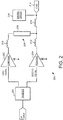
- the amplifier 200 is a Doherty amplifier that receives an RF input and drives an amplified signal to a load 216 (e.g., an antenna).
- the amplifier 200 includes a carrier amplifier 202, a peaking amplifier 204, a divider 205, and a combiner 206.
- the divider 206 receives an RF signal and generates two outputs that are 90 degrees out of phase with each other. These two outputs correspond to the first signal and second signal that are applied to the carrier amplifier 202 and peaking amplifier 204 respectively.
- the two outputs can be in the form of equal-power or unequal-power signals.
- the 90 degree phase difference can be provided by a phase delay element that applies a phase shift of about 90 degrees before outputting to the peaking amplifier 204.
- the 90 degree difference in phase allows the output of the peaking amplifier 204 to be in step with the carrier amplifier 202 output when combined by in the combiner 208.
- the divider 205 can be implemented with a power splitter and phase delay element, for example, implemented within the package or on a PCB to which the illustrated portion of the amplifier 200 is coupled.
- the carrier amplifier 202 can includes one or more carrier transistors
- the peaking amplifier 204 can includes one or more peaking transistors, with the outputs of the carrier and peaking transistors coupled to the combiner 206.
- the combiner 206 can be considered to include a transmission line 208 and inductances 210 and 212. This combiner 206 serves to the combine the outputs of the final (or single) stage carrier transistor in the carrier amplifier 202 and peaking transistor in the peaking amplifier 204 such that the combined output can be delivered to the load 216. To facilitate that this, the combiner 206 is coupled to the load 216 through inductance 214.
- the combiner 206 also provides an impedance inverter between the outputs of the carrier amplifier 202 and the peaking amplifier 204.
- Using the combiner 206 to provide an impedance inverter between the amplifiers 202 and 204 can improve efficiency at the operational frequency of the amplifier 200. Specifically, the efficiency can be improved at both back-off and peak power.
- the impedance inverter effectively changes the impedance seen by the carrier amplifier 202 to provide an optimal load to the carrier amplifier 202 at and around the operational frequency. This effectively adjusts the output of the peaking amplifier 204, and thus improves the efficiency of the amplifier 200.
- the inductances 210 and 212 in the combiner 206 can be provided by bond wire arrays used to couple the amplifiers 202 and 204 (e.g., drain terminals of the associated transistors) to the transmission line 208.
- the carrier amplifier 202, the peaking amplifier 204 and the transmission line 208 are provided on separate semiconductor dies or substrates. Providing the transmission line 208 on a die or substrate that is separate from the active die(s) on which the carrier amplifier 202 and peaking amplifier 204 reside can enable the use of different frequency and power levels when compared to a fully integrated implementation.
- the thickness and material properties of the dies or substrates used for amplifiers 202 and 204 and the transmission line 208 can each be selected based on their individual frequency and power requirements. More specifically, in some embodiments the dielectric thickness and constant used in the die or other substrate of the transmission line 208 can be specifically selected for optimal performance of the combiner 206. In such an embodiment, the separate dies or substrates would be packaged together in one device package, with the connection between dies and/or substrates in the package provided by bond wires. Thus, the bond wires can provide at least part of the inductances represented by inductances 210 and 212. Of course, it should be noted that other elements can provide all or part or all of those inductances in other embodiments.
- the inductance 214 can be provided by bond wires used to couple the transmission line 208 to a package lead (e.g., an output lead). That package lead can then provide the connection to the load 216 and a biasing circuit 218.
- the biasing circuit 218 provides a shared bias voltage to the drains of transistors in both the carrier amplifier 202 and the peaking amplifier 204. An example of such a shared bias voltage will be discussed with reference to FIG. 4 .
- the amplifier may include separate biasing circuits and/or one or more bias leads that are distinct from the output lead.
- the carrier amplifier 202 and peaking amplifier 204 would be implemented with suitable RF-capable transistors with relatively high power capability.
- the carrier amplifier 202 and peaking amplifier 204 can be implemented with Gallium Nitride (GaN) transistors or laterally diffused metal oxide semiconductor (LDMOS) transistors.
- the "input" of such a transistor is the control terminal (e.g., a gate terminal, "G") of the transistor
- the "output" of a transistor is a current carrying terminal (e.g., a drain terminal, "D", or source terminal, "S”) of the transistor.
- the other current carrying terminal e.g., the source or drain terminal
- is coupled to a ground node of the device e.g., to the device package substrate or flange.
- the inductances 210 and 212 can be relatively small compared to conventional amplifiers in which the combiner and its associated connections are made outside the package. Furthermore, by adjusting the electrical length (between first and second ends of the transmission line 208) and number of bond wires the values of the inductances 210 and 212 can be selected to provide an accurate impedance inverter at the operational frequency.
- the transistors implementing the carrier amplifier 202 and peaking amplifier 204 can each have intrinsic capacitances, such as drain-to-source capacitance (C DS ). These intrinsic capacitances are inherent in the transistors, and in implementing the combiner 206 the effects of the intrinsic capacitances are taken into account. This can be accomplished by selecting appropriate configurations for the inductances 210 and 212 and the transmission line 208. Specifically, the length of the transmission line 208 and physical characteristics of the bond wires used to couple the transmission line 208 to the transistors 202 and 204 are selected to account for the intrinsic capacitances C DS of the transistors in the amplifiers 202 and 204 in providing the impedance inverter.
- C DS drain-to-source capacitance
- the electrical length of the transmission line 208 and the inductances of the bond wires are selected such that the total phase shift provided by the transmission line 208 and the bond wire inductances between the outputs of the carrier amplifier 202 and peaking amplifier 204 is about 90 degrees and thus the combination of the transmission line 208 and the bond wires behaves as an impedance inverter.
- the transmission line 208 may have a length (between first and second ends) that is less than about 1 ⁇ 4 wavelength of an RF signal at a center operational frequency of the amplifier 200, where the bond wires will provide the additional inductances needed for effective impedance inverting at that frequency.
- the exact division between bond-wire inductance and transmission line impedance will typically depend on the specific implementation and frequency.
- the transmission line length is configured to provide between about 45 degrees to about 80 degrees of phase shift.
- Such an embodiment can be provided by implementing the transmission line 208 to have a length between about 0.5 to about 0.9 of 1 ⁇ 4 wavelength of an RF signal at a center operational frequency of the amplifier.
- the length and shape of the individual bond wires can be used to provide phase compensation.
- an array of graded bond wires can be used.
- graded bond wires the length of the individual bond wires varies in from one end of the array to the other.
- the individual bond wires can have a longer length near the end of the transmission line, and can get progressively shorter the closer to the center.
- Such a grading of the bond wires in the vertical dimension can be used to provide phase compensation of the signals in the combiner, and again can provide improved performance compared to a device that uses only lumped elements that are extremal to the package as a combiner.
- the transmission line 208 can be implemented in a variety of ways.
- the transmission line 208 can be implemented as one or more conductors in an integrated passive device (IPD).
- IPDs are formed using wafer-level or die-level fabrication techniques such as photolithography.
- the transmission line 208 can be formed on a wafer by depositing and patterning a conductive material to have the selected length and other desirable features. The wafer is then singulated to define a separate die that includes the transmission line 208, and that die is packaged (e.g., coupled to the package flange or substrate) with the other elements of the amplifier 200.
- the electrical connection between the formed transmission line 208 on the die and the other elements can be provided by bond wires.
- the transmission line 208 can be implemented as a conductor defined on a PCB substrate.
- the transmission line 208 can be printed on the PCB substrate to have the selected length, and then placed in the package (e.g., coupled to the package flange or substrate) with the other elements of the amplifier 200.
- the connections between the printed transmission line 208 and the other elements can be provided by bond wires.
- the transmission line 208 can be implemented with a microstrip line.
- a microstrip line is a type of transmission line that includes a conductive strip that is separated from a ground plane by a dielectric layer.
- Microstrip lines can be formed on a variety of substrates, including PCB substrates and semiconductor wafer/die substrates, and with a variety of manufacturing techniques.
- the microstrip line is formed with a length selected to provide a portion of an impedance inverter between the transistor outputs.
- the transmission line 208 can be formed as a microstrip line of the selected length, and then placed in the package with other elements of the amplifier 200.
- the connections between the printed transmission line 208 and the other elements can again be provided by bond wires.
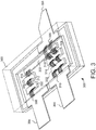
- FIG. 3 a perspective, cut-away view of an exemplary device 300 that includes a portion of an amplifier is illustrated.
- the device 300 includes a package 302, input leads 304 and 306, bond wire arrays 308, 310, 312, 314, 316, 318 and 320, a transmission line 322 and an output lead 324. Also included are a carrier transistor die 326, a peaking transistor die 328, and capacitor die 330 and 332, with the capacitor die 330 and 332 forming portions of input matching networks.
- device 300 is a simplified representation of a portion of an amplifier, and in a more typical implementation the amplifier would include additional features not illustrated in FIG. 3 .
- the package 302 includes a package substrate (e.g., formed of PCB materials with various conductive features) or flange (e.g., a rigid conductive component) to which the transistor die 326, 328, capacitors 330, 332, and the transmission line 322 (e.g., a substrate or IPD that includes the transmission line 322) are coupled.
- the package substrate or flange may provide an electrical ground reference for the device (e.g., for the capacitors 330, 332 and for the transistor die 326, 324 (e.g., more specifically to the sources of the carrier and peaking transistors).
- the package 302 also may include an isolator that electrically isolates the package substrate or flange from the leads 304, 306, 324, or alternatively may include encapsulation that provides such electrical isolation.
- the package 302 may be an air-cavity package or an overmolded (encapsulated) package, in various embodiments.
- the first input lead 304 is configured to receive a carrier signal
- the second input lead 306 is configured to receive a peaking signal.
- the bond wires 308, 312 and the capacitor 330 form portions of a first input matching network coupled between the input lead 304 and the input (e.g., gate) of the carrier transistor die 326.
- the bond wires 316 couple the output (e.g., drain) of the carrier transistor die 326 to the transmission line 322.
- the bond wires 310, 314 and the capacitor 3332 form portions of a second input matching network coupled between the second input lead 306 and the input (e.g., gate) of the peaking transistor die 3.
- the bond wires 318 couple the output (e.g., drain) of the peaking transistor die 328 to the transmission line 322.
- the bond wires 320 couple the outputs of the carrier transistor die 326 and peaking transistor die 328 to the output lead 324. More specifically, in the illustrated embodiment, bond wires 320 coupled the output of the peaking transistor die 328 to the output lead 324 (and the output of the carrier transistor die 326 is coupled to the output of the peaking transistor die 328 through the transmission line 322.
- bond wires would be selected based on the power handling requirements and the desired inductance of the bond wires. Thus, for connections that require more power handling ability (e.g., connections to the peaking transistor) more bond wires can be provided.
- the carrier and peaking transistor die 326, 328 are illustrated as separate die, an alternate example, not covered by the invention, may have the carrier and peaking transistors implemented on a single die.
- bond wires 316 are coupled to a first end of transmission line 322, and bond wires 318 are coupled to a second end of transmission line 322.
- the second end of transmission line 322 further is coupled (through bond wires 318 and 320 to the output lead 324. Accordingly, the output signal from the carrier transistor on the carrier transistor die 326 travels through bond wires 316, through the transmission line 322 from the first end to the second end, and through bond wires 318 to the output of the peaking transistor on the peaking transistor die 328.
- the combination of the bond wires 316, the length of the transmission line 322 (between first and second ends), and the bond wires 318 provide the impedance inversion (and about 90 degree phase delay) to the signal produced at the output of the carrier transistor.
- the output of the peaking transistor on the peaking transistor die 328 serves as the combining node for the output carrier and peaking signals.
- the output carrier and peaking signals are combined in-phase at the combining node (e.g., at the output of the peaking transistor).
- the bond wires 316 and 318, and the transmission line 322 can be considered to be part of a combiner (e.g., combiner 206) that serves to the combine the output signals produced by the carrier transistor and peaking transistor such that the combined output can be delivered to the load output lead 324.
- a combiner e.g., combiner 206 that serves to the combine the output signals produced by the carrier transistor and peaking transistor such that the combined output can be delivered to the load output lead 324.
- the bond wires 316 and 318, and the transmission line 322 are encased in the package 302 with the carrier transistor die 326 and peaking transistor die 328. Configured in this way, the combiner facilitates a Doherty amplifier that has a relatively high fractional bandwidth.
- the transmission line 322 may be on a separate substrate (e.g., die) from the transistor die 326, 328, the use of different frequencies and power levels in the various die or substrates are enabled.
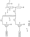
- FIG. 4 a circuit diagram representing a portion of an exemplary amplifier 400 is illustrated.
- the amplifier 400 is again a Doherty amplifier that receives a carrier signal and a peaking signal and drives a combined signal to a load 416.
- the amplifier 400 includes one or more carrier transistors 402, one or more peaking transistors 404 and a combiner 406.
- the combiner 406 can be considered to include a transmission line 408 and inductances 410 and 412. This combiner 406 again serves to the combine the output signals produced by the carrier transistor 402 and peaking transistor 404 such that the combined output can be delivered through inductance 414 to the load 416.
- a biasing circuit 418 is coupled to the inductance 414.
- the biasing circuit 418 includes a DC voltage source V DC , a quarter-wave transformer 420, and a capacitor 422 coupled to ground.
- the biasing circuit 418 provides a DC bias voltage to both the drain of the carrier transistor 402 and the drain of the peaking transistor 404.
- the quarter-wave transformer 420 acts to provide an open circuit to the output lead at the operational frequency 1/ ⁇ , preventing the RF energy from flowing through the biasing circuit 418 to ground.
- the capacitor 422 prevents the DC bias voltage from shorting to ground.
- the biasing circuit 418 provides a shared DC bias voltage V DC to the drains of both the carrier transistor 402 and the peaking transistor 404. Having the common bias voltage V DC applied to both transistors through a shared input can provide improved ease of biasing and reduced bias network complexity.
- the embodiments described herein can provide semiconductor devices, and particularly amplifiers, with improved performance.
- the embodiments described herein include amplifiers that are typically used in radio frequency (RF) applications.
- the amplifiers described herein use a combiner that is implemented inside the device package in a way that facilitates improved amplifier bandwidth.
- the amplifiers can be implemented with a combiner that includes a transmission line inside the device package, where the transmission line has a length between first and second ends that is configured to provide an impedance inverter between the outputs of transistors in the amplifier. So configured, the combiner can facilitate an amplifier with a relatively high fractional bandwidth and relatively high efficiency. Furthermore, such an amplifier can be provided with a reduced size and more consistent circuit performance.
- embodiments may include an "inverted" Doherty amplifier implementation (e.g., in which a 90 degree phase delay is applied to the input carrier signal prior to amplification, and a corresponding 90 degree phase delay is applied to the output peaking signal after amplification).
- embodiments include single-stage and multiple-stage amplifiers.
- the main and peaking transistors may be implemented on separate die or on the same die, in various embodiments.
- a Doherty amplifier as claimed in claim 1 is provided.
- the transmission line comprises a conductor defined on a printed circuit board (PCB).
- the transmission line comprises a conductive feature of an integrated passive device (IPD).
- the transmission line comprises a microstrip line.
- the transmission line is formed on a substrate distinct from a die on which either the first transistor is formed, the second transistor is formed, or both the first and second transistor is formed.
- the transmission line has a length between 0.5 to 0.9 of a 1 ⁇ 4 wavelength of a radio frequency (RF) signal at a center operational frequency of the amplifier.
- RF radio frequency
- the amplifier further comprises a biasing circuit.
- the biasing circuit is coupled to both the first transistor output and the second transistor output to provide a shared bias voltage to the first transistor and the second transistor.
- node means any internal or external reference point, connection point, junction, signal line, conductive element, or the like, at which a given signal, logic level, voltage, data pattern, current, or quantity is present.
- two or more nodes may be realized by one physical element (and two or more signals can be multiplexed, modulated, or otherwise distinguished even though received or output at a common node).
Landscapes
- Engineering & Computer Science (AREA)
- Power Engineering (AREA)
- Amplifiers (AREA)
- Microwave Amplifiers (AREA)
Claims (6)
- Doherty-Verstärker, der Folgendes umfasst:ein Vorrichtungsgehäuse (108, 302), das eine Ausgangsleitung (110, 324), eine erste Eingangsleitung (304), die konfiguriert ist, ein Trägersignal zu empfangen, und eine zweite Eingangsleitung (306), die konfiguriert ist, ein Spitzenwertsignal zu empfangen, aufweist, wobei das Vorrichtungsgehäuse Folgendes umgibt:einen Trägertransistor (326), der auf einem Trägertransistor-Chip gebildet ist und einen Trägertransistor-Eingang, der mit der ersten Eingangsleitung verbunden ist, und einen Trägertransistor-Ausgang besitzt;einen Spitzenwerttransistor (328), der auf einem Spitzenwerttransistor-Chip gebildet ist und einen Spitzenwerttransistor-Eingang, der mit der zweiten Eingangsleitung verbunden ist, und einen Spitzenwerttransistor-Ausgang besitzt;eine Übertragungsleitung (208, 322, 408), die eine Länge besitzt, wobei die Übertragungsleitung auf einem Substrat gebildet ist, das von dem Trägertransistor-Chip (306) und von dem Spitzenwerttransistor-Chip (328) verschieden ist;eine erste Gruppe von Bond-Drähten (316), die den Trägertransistor-Ausgang mit einem ersten Ende der Übertragungsleitung verbinden;eine zweite Gruppe von Bond-Drähten (318), die den Spitzenwerttransistor-Ausgang mit einem zweiten Ende der Übertragungsleitung verbinden;wobei eine Länge der Übertragungsleitung zwischen dem ersten und dem zweiten Ende so konfiguriert ist, dass in Kombination mit einer parasitären Kapazität des Trägertransistors, einer parasitären Kapazität des Spitzenwerttransistors, der ersten Gruppe von Bond-Drähten und der zweiten Gruppe von Bond-Drähten ein Impedanzwandler zwischen dem Trägertransistor-Ausgang und dem Spitzenwerttransistor-Ausgang bereitgestellt wird,gekennzeichnet durch eine dritte Gruppe von Bond-Drähten (320), die den Spitzenwerttransistor-Ausgang mit der Ausgangsleitung verbinden.
- Doherty-Verstärker nach Anspruch 1, wobei die Übertragungsleitung einen Leiter umfasst, der auf einer gedruckten Leiterplatte, PCB, definiert ist.
- Doherty-Verstärker nach Anspruch 1, wobei die Übertragungsleitung ein leitendes Merkmal einer integrierten passiven Vorrichtung, IPD, umfasst.
- Doherty-Verstärker nach Anspruch 1, wobei die Übertragungsleitung eine Mikrostreifenleitung umfasst.
- Doherty-Verstärker nach einem der Ansprüche 1 bis 4, wobei die Übertragungsleitung eine Länge im Bereich des 0,5- bis 0,9-Fachen einer Viertelwellenlänge eines Hochfrequenzsignals, HF-Signals, bei einer Betriebsmittenfrequenz des Verstärkers besitzt.
- Doherty-Verstärker nach einem der Ansprüche 1 bis 5, der ferner eine Vorspannungsschaltung umfasst, wobei die Vorspannungsschaltung sowohl mit dem ersten Transistorausgang als auch mit dem zweiten Transistorausgang verbunden ist, um eine gemeinsam genutzte Vorspannung für den ersten Transistor und den zweiten Transistor bereitzustellen.
Applications Claiming Priority (1)
| Application Number | Priority Date | Filing Date | Title |
|---|---|---|---|
| US14/966,922 US9621115B1 (en) | 2015-12-11 | 2015-12-11 | Amplifier devices with in-package transmission line combiner |
Publications (3)
| Publication Number | Publication Date |
|---|---|
| EP3179628A2 EP3179628A2 (de) | 2017-06-14 |
| EP3179628A3 EP3179628A3 (de) | 2017-08-23 |
| EP3179628B1 true EP3179628B1 (de) | 2021-04-28 |
Family
ID=57530603
Family Applications (1)
| Application Number | Title | Priority Date | Filing Date |
|---|---|---|---|
| EP16203004.3A Active EP3179628B1 (de) | 2015-12-11 | 2016-12-08 | Verstärkervorrichtungen mit übertragungsleitungskombinator in einem gehäuse |
Country Status (2)
| Country | Link |
|---|---|
| US (1) | US9621115B1 (de) |
| EP (1) | EP3179628B1 (de) |
Cited By (3)
| Publication number | Priority date | Publication date | Assignee | Title |
|---|---|---|---|---|
| WO2022235535A1 (en) * | 2021-05-06 | 2022-11-10 | Wolfspeed, Inc. | Output-integrated transistor amplifier device packages incorporating internal connections |
| US11888448B2 (en) | 2019-12-30 | 2024-01-30 | Macom Technology Solutions Holdings, Inc. | Low-load-modulation broadband amplifier |
| US12381515B2 (en) | 2017-04-24 | 2025-08-05 | Macom Technology Solutions Holdings, Inc. | Symmetrical Doherty power amplifier having improved efficiency |
Families Citing this family (23)
| Publication number | Priority date | Publication date | Assignee | Title |
|---|---|---|---|---|
| US10284146B2 (en) | 2016-12-01 | 2019-05-07 | Nxp Usa, Inc. | Amplifier die with elongated side pads, and amplifier modules that incorporate such amplifier die |
| US10284147B2 (en) | 2016-12-15 | 2019-05-07 | Nxp Usa, Inc. | Doherty amplifiers and amplifier modules with shunt inductance circuits that affect transmission line length between carrier and peaking amplifier outputs |
| US10381984B2 (en) | 2016-12-15 | 2019-08-13 | Nxp Usa, Inc. | Amplifiers and amplifier modules with shunt inductance circuits that include high-Q capacitors |
| US11233483B2 (en) | 2017-02-02 | 2022-01-25 | Macom Technology Solutions Holdings, Inc. | 90-degree lumped and distributed Doherty impedance inverter |
| WO2018142176A1 (en) * | 2017-02-02 | 2018-08-09 | Macom Technology Solutions Holdings, Inc. | Methods for combining doherty amplifier signals with 90-degree lumped and distributed impedance inverters |
| EP3616320B1 (de) | 2017-04-24 | 2023-11-08 | MACOM Technology Solutions Holdings, Inc. | Invertierter doherty-leistungsverstärker mit grossen hf- und momentanbandbreiten |
| WO2018197917A1 (en) | 2017-04-24 | 2018-11-01 | Macom Technology Solutions Holdings, Inc. | Inverted doherty power amplifier with large rf fractional and instantaneous bandwiths |
| FR3070100A1 (fr) | 2017-08-14 | 2019-02-15 | Macom Technology Solutions Holdings, Inc. | Architecture d'amplificateur de puissance sans modulation, a large bande et a haut rendement |
| WO2019069115A1 (en) | 2017-10-02 | 2019-04-11 | Macom Technology Solutions Holdings, Inc. | HIGH PERFORMANCE POWER AMPLIFIER WITHOUT CHARGE MODULATION |
| US10250197B1 (en) * | 2017-11-06 | 2019-04-02 | Nxp Usa, Inc. | Multiple-stage power amplifiers implemented with multiple semiconductor technologies |
| US10594266B2 (en) * | 2017-12-04 | 2020-03-17 | Nxp Usa, Inc. | Multiple-path amplifier with series component along inverter between amplifier outputs |
| US10826194B2 (en) | 2018-02-21 | 2020-11-03 | International Business Machines Corporation | Scalable phased array package |
| US10784563B2 (en) | 2018-02-21 | 2020-09-22 | International Business Machines Corporation | Scalable phased array package |
| US10629552B2 (en) | 2018-04-30 | 2020-04-21 | Nxp Usa, Inc. | Amplifiers and amplifier modules with ground plane height variation structures |
| US11705869B2 (en) | 2018-10-05 | 2023-07-18 | Macom Technology Solutions Holdings, Inc. | Low-load-modulation power amplifier |
| EP3664287A1 (de) * | 2018-12-05 | 2020-06-10 | NXP USA, Inc. | Integral geformter mehrpfadiger leistungsverstärker mit kombinierender knotenstruktur auf einem chip |
| US11223336B2 (en) | 2018-12-05 | 2022-01-11 | Nxp Usa, Inc. | Power amplifier integrated circuit with integrated shunt-l circuit at amplifier output |
| US11018629B2 (en) * | 2019-06-24 | 2021-05-25 | Nxp Usa, Inc. | Integrated multiple-path power amplifier |
| US11190146B2 (en) | 2019-11-19 | 2021-11-30 | Nxp Usa, Inc. | Doherty power amplifier devices having intergrated output combining networks |
| EP3836210B1 (de) | 2019-12-10 | 2025-06-18 | NXP USA, Inc. | Integrierter mehrwegleistungsverstärker |
| US12028022B2 (en) | 2020-12-10 | 2024-07-02 | Macom Technology Solutions Holdings, Inc. | Hybrid power amplifier with GaN-on-Si and GaN-on-SiC circuits |
| US12603622B2 (en) | 2021-10-29 | 2026-04-14 | Analog Devices International Unlimited Company | Apparatus and methods for radio frequency amplifiers |
| US20250006688A1 (en) * | 2023-06-27 | 2025-01-02 | Sumitomo Electric Device Innovations, Inc. | Output matching network to reduce self and mutual inductances of output inductive components in a cavity package |
Family Cites Families (16)
| Publication number | Priority date | Publication date | Assignee | Title |
|---|---|---|---|---|
| US5973567A (en) * | 1997-06-16 | 1999-10-26 | Hughes Electronics Corporation | Tunable impedance matching network for a mic power amplifier module |
| EP1532731B1 (de) | 2002-08-19 | 2011-09-21 | Nxp B.V. | Hochleistungs-doherty-verstärker |
| US6833761B2 (en) * | 2003-02-28 | 2004-12-21 | Freescale Semiconductor, Inc. | Amplifier apparatus and method thereof |
| WO2006006119A1 (en) * | 2004-07-08 | 2006-01-19 | Koninklijke Philips Electronics N.V. | Integrated doherty type amplifier arrangement with integrated feedback |
| CN101617403B (zh) * | 2006-04-26 | 2012-09-26 | Nxp股份有限公司 | 高功率集成射频放大器 |
| WO2008062371A2 (en) * | 2006-11-23 | 2008-05-29 | Nxp B.V. | Integrated doherty type amplifier arrangement with high power efficiency |
| US7764120B2 (en) * | 2008-08-19 | 2010-07-27 | Cree, Inc. | Integrated circuit with parallel sets of transistor amplifiers having different turn on power levels |
| KR101097605B1 (ko) * | 2009-11-04 | 2011-12-22 | 알.에프 에이치아이씨 주식회사 | 도허티 증폭기 |
| EP2339746B1 (de) * | 2009-12-15 | 2013-02-20 | Nxp B.V. | Doherty-Verstärker mit zusammengesetzter Übertragungseigenschaft mit mehreren Spitzenverstärkern |
| JP2012029239A (ja) * | 2010-07-27 | 2012-02-09 | Sumitomo Electric Device Innovations Inc | ドハティ増幅器 |
| EP2458730B8 (de) | 2010-11-29 | 2015-08-05 | Nxp B.V. | Hochfrequenzverstärker |
| US8717102B2 (en) * | 2011-09-27 | 2014-05-06 | Infineon Technologies Ag | RF device with compensatory resonator matching topology |
| US8717099B2 (en) * | 2012-03-16 | 2014-05-06 | Infineon Technologies Ag | Wideband doherty amplifier circuit with peaking impedance absorption |
| US8653889B1 (en) * | 2012-09-06 | 2014-02-18 | Alcatel Lucent | Doherty amplifier having compact output matching and combining networks |
| US9531329B2 (en) * | 2013-09-12 | 2016-12-27 | Nec Corporation | Power amplifier and transmission apparatus |
| EP2869463B1 (de) * | 2013-10-31 | 2016-01-06 | Samba Holdco Netherlands B.V. | Doherty-Verstärker-Struktur |
-
2015
- 2015-12-11 US US14/966,922 patent/US9621115B1/en active Active
-
2016
- 2016-12-08 EP EP16203004.3A patent/EP3179628B1/de active Active
Non-Patent Citations (1)
| Title |
|---|
| None * |
Cited By (4)
| Publication number | Priority date | Publication date | Assignee | Title |
|---|---|---|---|---|
| US12381515B2 (en) | 2017-04-24 | 2025-08-05 | Macom Technology Solutions Holdings, Inc. | Symmetrical Doherty power amplifier having improved efficiency |
| US11888448B2 (en) | 2019-12-30 | 2024-01-30 | Macom Technology Solutions Holdings, Inc. | Low-load-modulation broadband amplifier |
| WO2022235535A1 (en) * | 2021-05-06 | 2022-11-10 | Wolfspeed, Inc. | Output-integrated transistor amplifier device packages incorporating internal connections |
| US11936342B2 (en) | 2021-05-06 | 2024-03-19 | Macom Technology Solutions Holdings, Inc. | Output-integrated transistor amplifier device packages incorporating internal connections |
Also Published As
| Publication number | Publication date |
|---|---|
| EP3179628A3 (de) | 2017-08-23 |
| EP3179628A2 (de) | 2017-06-14 |
| US9621115B1 (en) | 2017-04-11 |
Similar Documents
| Publication | Publication Date | Title |
|---|---|---|
| US9621115B1 (en) | Amplifier devices with in-package transmission line combiner | |
| US11108362B2 (en) | Multiple-path RF amplifiers with angularly offset signal path directions, and methods of manufacture thereof | |
| US10784824B2 (en) | Amplifiers and related integrated circuits | |
| EP3331161B1 (de) | Verstärkermatrize mit länglichen seitenflächen und verstärkermodule mit solch einer verstärkermatrize | |
| US10284147B2 (en) | Doherty amplifiers and amplifier modules with shunt inductance circuits that affect transmission line length between carrier and peaking amplifier outputs | |
| US10381984B2 (en) | Amplifiers and amplifier modules with shunt inductance circuits that include high-Q capacitors | |
| US9077285B2 (en) | Electronic devices with multiple amplifier stages and methods of their manufacture | |
| US9531328B2 (en) | Amplifiers with a short phase path, packaged RF devices for use therein, and methods of manufacture thereof | |
| US12159845B2 (en) | Transistor with integrated passive components | |
| CN112953401A (zh) | 集成多路径功率放大器 | |
| US10250196B2 (en) | Amplifier devices with back-off power optimization | |
| EP3780387B1 (de) | Integrierter mehrwegleistungsverstärker mit ineinandergreifenden transistoren | |
| EP4207276A1 (de) | Leistungstransistorvorrichtungen und verstärker mit eingangsseitigen harmonischen abschlussschaltungen | |
| EP3611839A1 (de) | Verstärker mit breitbandiger impedanzanpassung und verfahren zur herstellung davon | |
| US11936342B2 (en) | Output-integrated transistor amplifier device packages incorporating internal connections | |
| US11967936B2 (en) | Output-integrated transistor device packages |
Legal Events
| Date | Code | Title | Description |
|---|---|---|---|
| PUAI | Public reference made under article 153(3) epc to a published international application that has entered the european phase |
Free format text: ORIGINAL CODE: 0009012 |
|
| STAA | Information on the status of an ep patent application or granted ep patent |
Free format text: STATUS: THE APPLICATION HAS BEEN PUBLISHED |
|
| AK | Designated contracting states |
Kind code of ref document: A2 Designated state(s): AL AT BE BG CH CY CZ DE DK EE ES FI FR GB GR HR HU IE IS IT LI LT LU LV MC MK MT NL NO PL PT RO RS SE SI SK SM TR |
|
| AX | Request for extension of the european patent |
Extension state: BA ME |
|
| PUAL | Search report despatched |
Free format text: ORIGINAL CODE: 0009013 |
|
| AK | Designated contracting states |
Kind code of ref document: A3 Designated state(s): AL AT BE BG CH CY CZ DE DK EE ES FI FR GB GR HR HU IE IS IT LI LT LU LV MC MK MT NL NO PL PT RO RS SE SI SK SM TR |
|
| AX | Request for extension of the european patent |
Extension state: BA ME |
|
| RIC1 | Information provided on ipc code assigned before grant |
Ipc: H03F 1/02 20060101AFI20170720BHEP |
|
| STAA | Information on the status of an ep patent application or granted ep patent |
Free format text: STATUS: REQUEST FOR EXAMINATION WAS MADE |
|
| 17P | Request for examination filed |
Effective date: 20180223 |
|
| RBV | Designated contracting states (corrected) |
Designated state(s): AL AT BE BG CH CY CZ DE DK EE ES FI FR GB GR HR HU IE IS IT LI LT LU LV MC MK MT NL NO PL PT RO RS SE SI SK SM TR |
|
| STAA | Information on the status of an ep patent application or granted ep patent |
Free format text: STATUS: EXAMINATION IS IN PROGRESS |
|
| 17Q | First examination report despatched |
Effective date: 20180626 |
|
| GRAP | Despatch of communication of intention to grant a patent |
Free format text: ORIGINAL CODE: EPIDOSNIGR1 |
|
| STAA | Information on the status of an ep patent application or granted ep patent |
Free format text: STATUS: GRANT OF PATENT IS INTENDED |
|
| INTG | Intention to grant announced |
Effective date: 20201113 |
|
| GRAS | Grant fee paid |
Free format text: ORIGINAL CODE: EPIDOSNIGR3 |
|
| GRAA | (expected) grant |
Free format text: ORIGINAL CODE: 0009210 |
|
| STAA | Information on the status of an ep patent application or granted ep patent |
Free format text: STATUS: THE PATENT HAS BEEN GRANTED |
|
| AK | Designated contracting states |
Kind code of ref document: B1 Designated state(s): AL AT BE BG CH CY CZ DE DK EE ES FI FR GB GR HR HU IE IS IT LI LT LU LV MC MK MT NL NO PL PT RO RS SE SI SK SM TR |
|
| REG | Reference to a national code |
Ref country code: GB Ref legal event code: FG4D |
|
| REG | Reference to a national code |
Ref country code: CH Ref legal event code: EP |
|
| REG | Reference to a national code |
Ref country code: DE Ref legal event code: R096 Ref document number: 602016056800 Country of ref document: DE |
|
| REG | Reference to a national code |
Ref country code: AT Ref legal event code: REF Ref document number: 1388291 Country of ref document: AT Kind code of ref document: T Effective date: 20210515 |
|
| REG | Reference to a national code |
Ref country code: IE Ref legal event code: FG4D |
|
| REG | Reference to a national code |
Ref country code: LT Ref legal event code: MG9D |
|
| REG | Reference to a national code |
Ref country code: AT Ref legal event code: MK05 Ref document number: 1388291 Country of ref document: AT Kind code of ref document: T Effective date: 20210428 |
|
| PG25 | Lapsed in a contracting state [announced via postgrant information from national office to epo] |
Ref country code: NL Free format text: LAPSE BECAUSE OF FAILURE TO SUBMIT A TRANSLATION OF THE DESCRIPTION OR TO PAY THE FEE WITHIN THE PRESCRIBED TIME-LIMIT Effective date: 20210428 Ref country code: LT Free format text: LAPSE BECAUSE OF FAILURE TO SUBMIT A TRANSLATION OF THE DESCRIPTION OR TO PAY THE FEE WITHIN THE PRESCRIBED TIME-LIMIT Effective date: 20210428 Ref country code: FI Free format text: LAPSE BECAUSE OF FAILURE TO SUBMIT A TRANSLATION OF THE DESCRIPTION OR TO PAY THE FEE WITHIN THE PRESCRIBED TIME-LIMIT Effective date: 20210428 Ref country code: BG Free format text: LAPSE BECAUSE OF FAILURE TO SUBMIT A TRANSLATION OF THE DESCRIPTION OR TO PAY THE FEE WITHIN THE PRESCRIBED TIME-LIMIT Effective date: 20210728 Ref country code: AT Free format text: LAPSE BECAUSE OF FAILURE TO SUBMIT A TRANSLATION OF THE DESCRIPTION OR TO PAY THE FEE WITHIN THE PRESCRIBED TIME-LIMIT Effective date: 20210428 Ref country code: HR Free format text: LAPSE BECAUSE OF FAILURE TO SUBMIT A TRANSLATION OF THE DESCRIPTION OR TO PAY THE FEE WITHIN THE PRESCRIBED TIME-LIMIT Effective date: 20210428 |
|
| PG25 | Lapsed in a contracting state [announced via postgrant information from national office to epo] |
Ref country code: SE Free format text: LAPSE BECAUSE OF FAILURE TO SUBMIT A TRANSLATION OF THE DESCRIPTION OR TO PAY THE FEE WITHIN THE PRESCRIBED TIME-LIMIT Effective date: 20210428 Ref country code: RS Free format text: LAPSE BECAUSE OF FAILURE TO SUBMIT A TRANSLATION OF THE DESCRIPTION OR TO PAY THE FEE WITHIN THE PRESCRIBED TIME-LIMIT Effective date: 20210428 Ref country code: PL Free format text: LAPSE BECAUSE OF FAILURE TO SUBMIT A TRANSLATION OF THE DESCRIPTION OR TO PAY THE FEE WITHIN THE PRESCRIBED TIME-LIMIT Effective date: 20210428 Ref country code: NO Free format text: LAPSE BECAUSE OF FAILURE TO SUBMIT A TRANSLATION OF THE DESCRIPTION OR TO PAY THE FEE WITHIN THE PRESCRIBED TIME-LIMIT Effective date: 20210728 Ref country code: PT Free format text: LAPSE BECAUSE OF FAILURE TO SUBMIT A TRANSLATION OF THE DESCRIPTION OR TO PAY THE FEE WITHIN THE PRESCRIBED TIME-LIMIT Effective date: 20210830 Ref country code: LV Free format text: LAPSE BECAUSE OF FAILURE TO SUBMIT A TRANSLATION OF THE DESCRIPTION OR TO PAY THE FEE WITHIN THE PRESCRIBED TIME-LIMIT Effective date: 20210428 Ref country code: GR Free format text: LAPSE BECAUSE OF FAILURE TO SUBMIT A TRANSLATION OF THE DESCRIPTION OR TO PAY THE FEE WITHIN THE PRESCRIBED TIME-LIMIT Effective date: 20210729 Ref country code: IS Free format text: LAPSE BECAUSE OF FAILURE TO SUBMIT A TRANSLATION OF THE DESCRIPTION OR TO PAY THE FEE WITHIN THE PRESCRIBED TIME-LIMIT Effective date: 20210828 |
|
| REG | Reference to a national code |
Ref country code: NL Ref legal event code: MP Effective date: 20210428 |
|
| PG25 | Lapsed in a contracting state [announced via postgrant information from national office to epo] |
Ref country code: SK Free format text: LAPSE BECAUSE OF FAILURE TO SUBMIT A TRANSLATION OF THE DESCRIPTION OR TO PAY THE FEE WITHIN THE PRESCRIBED TIME-LIMIT Effective date: 20210428 Ref country code: SM Free format text: LAPSE BECAUSE OF FAILURE TO SUBMIT A TRANSLATION OF THE DESCRIPTION OR TO PAY THE FEE WITHIN THE PRESCRIBED TIME-LIMIT Effective date: 20210428 Ref country code: CZ Free format text: LAPSE BECAUSE OF FAILURE TO SUBMIT A TRANSLATION OF THE DESCRIPTION OR TO PAY THE FEE WITHIN THE PRESCRIBED TIME-LIMIT Effective date: 20210428 Ref country code: EE Free format text: LAPSE BECAUSE OF FAILURE TO SUBMIT A TRANSLATION OF THE DESCRIPTION OR TO PAY THE FEE WITHIN THE PRESCRIBED TIME-LIMIT Effective date: 20210428 Ref country code: DK Free format text: LAPSE BECAUSE OF FAILURE TO SUBMIT A TRANSLATION OF THE DESCRIPTION OR TO PAY THE FEE WITHIN THE PRESCRIBED TIME-LIMIT Effective date: 20210428 Ref country code: RO Free format text: LAPSE BECAUSE OF FAILURE TO SUBMIT A TRANSLATION OF THE DESCRIPTION OR TO PAY THE FEE WITHIN THE PRESCRIBED TIME-LIMIT Effective date: 20210428 Ref country code: ES Free format text: LAPSE BECAUSE OF FAILURE TO SUBMIT A TRANSLATION OF THE DESCRIPTION OR TO PAY THE FEE WITHIN THE PRESCRIBED TIME-LIMIT Effective date: 20210428 |
|
| REG | Reference to a national code |
Ref country code: DE Ref legal event code: R097 Ref document number: 602016056800 Country of ref document: DE |
|
| PLBE | No opposition filed within time limit |
Free format text: ORIGINAL CODE: 0009261 |
|
| STAA | Information on the status of an ep patent application or granted ep patent |
Free format text: STATUS: NO OPPOSITION FILED WITHIN TIME LIMIT |
|
| 26N | No opposition filed |
Effective date: 20220131 |
|
| PG25 | Lapsed in a contracting state [announced via postgrant information from national office to epo] |
Ref country code: IS Free format text: LAPSE BECAUSE OF FAILURE TO SUBMIT A TRANSLATION OF THE DESCRIPTION OR TO PAY THE FEE WITHIN THE PRESCRIBED TIME-LIMIT Effective date: 20210828 Ref country code: AL Free format text: LAPSE BECAUSE OF FAILURE TO SUBMIT A TRANSLATION OF THE DESCRIPTION OR TO PAY THE FEE WITHIN THE PRESCRIBED TIME-LIMIT Effective date: 20210428 |
|
| PG25 | Lapsed in a contracting state [announced via postgrant information from national office to epo] |
Ref country code: MC Free format text: LAPSE BECAUSE OF FAILURE TO SUBMIT A TRANSLATION OF THE DESCRIPTION OR TO PAY THE FEE WITHIN THE PRESCRIBED TIME-LIMIT Effective date: 20210428 Ref country code: IT Free format text: LAPSE BECAUSE OF FAILURE TO SUBMIT A TRANSLATION OF THE DESCRIPTION OR TO PAY THE FEE WITHIN THE PRESCRIBED TIME-LIMIT Effective date: 20210428 |
|
| REG | Reference to a national code |
Ref country code: CH Ref legal event code: PL |
|
| GBPC | Gb: european patent ceased through non-payment of renewal fee |
Effective date: 20211208 |
|
| REG | Reference to a national code |
Ref country code: BE Ref legal event code: MM Effective date: 20211231 |
|
| PG25 | Lapsed in a contracting state [announced via postgrant information from national office to epo] |
Ref country code: LU Free format text: LAPSE BECAUSE OF NON-PAYMENT OF DUE FEES Effective date: 20211208 Ref country code: IE Free format text: LAPSE BECAUSE OF NON-PAYMENT OF DUE FEES Effective date: 20211208 Ref country code: GB Free format text: LAPSE BECAUSE OF NON-PAYMENT OF DUE FEES Effective date: 20211208 |
|
| PG25 | Lapsed in a contracting state [announced via postgrant information from national office to epo] |
Ref country code: FR Free format text: LAPSE BECAUSE OF NON-PAYMENT OF DUE FEES Effective date: 20211231 Ref country code: BE Free format text: LAPSE BECAUSE OF NON-PAYMENT OF DUE FEES Effective date: 20211231 |
|
| PG25 | Lapsed in a contracting state [announced via postgrant information from national office to epo] |
Ref country code: LI Free format text: LAPSE BECAUSE OF NON-PAYMENT OF DUE FEES Effective date: 20211231 Ref country code: CH Free format text: LAPSE BECAUSE OF NON-PAYMENT OF DUE FEES Effective date: 20211231 |
|
| PG25 | Lapsed in a contracting state [announced via postgrant information from national office to epo] |
Ref country code: HU Free format text: LAPSE BECAUSE OF FAILURE TO SUBMIT A TRANSLATION OF THE DESCRIPTION OR TO PAY THE FEE WITHIN THE PRESCRIBED TIME-LIMIT; INVALID AB INITIO Effective date: 20161208 |
|
| PG25 | Lapsed in a contracting state [announced via postgrant information from national office to epo] |
Ref country code: CY Free format text: LAPSE BECAUSE OF FAILURE TO SUBMIT A TRANSLATION OF THE DESCRIPTION OR TO PAY THE FEE WITHIN THE PRESCRIBED TIME-LIMIT Effective date: 20210428 |
|
| P01 | Opt-out of the competence of the unified patent court (upc) registered |
Effective date: 20230725 |
|
| PG25 | Lapsed in a contracting state [announced via postgrant information from national office to epo] |
Ref country code: MK Free format text: LAPSE BECAUSE OF FAILURE TO SUBMIT A TRANSLATION OF THE DESCRIPTION OR TO PAY THE FEE WITHIN THE PRESCRIBED TIME-LIMIT Effective date: 20210428 |
|
| PG25 | Lapsed in a contracting state [announced via postgrant information from national office to epo] |
Ref country code: TR Free format text: LAPSE BECAUSE OF FAILURE TO SUBMIT A TRANSLATION OF THE DESCRIPTION OR TO PAY THE FEE WITHIN THE PRESCRIBED TIME-LIMIT Effective date: 20210428 |
|
| PG25 | Lapsed in a contracting state [announced via postgrant information from national office to epo] |
Ref country code: MT Free format text: LAPSE BECAUSE OF FAILURE TO SUBMIT A TRANSLATION OF THE DESCRIPTION OR TO PAY THE FEE WITHIN THE PRESCRIBED TIME-LIMIT Effective date: 20210428 |
|
| PGFP | Annual fee paid to national office [announced via postgrant information from national office to epo] |
Ref country code: DE Payment date: 20251126 Year of fee payment: 10 |