EP3179525A1 - Semiconductor device and method for manufacturing same - Google Patents
Semiconductor device and method for manufacturing same Download PDFInfo
- Publication number
- EP3179525A1 EP3179525A1 EP15830533.4A EP15830533A EP3179525A1 EP 3179525 A1 EP3179525 A1 EP 3179525A1 EP 15830533 A EP15830533 A EP 15830533A EP 3179525 A1 EP3179525 A1 EP 3179525A1
- Authority
- EP
- European Patent Office
- Prior art keywords
- metal substrate
- resin
- semiconductor
- producing
- reflector
- Prior art date
- Legal status (The legal status is an assumption and is not a legal conclusion. Google has not performed a legal analysis and makes no representation as to the accuracy of the status listed.)
- Granted
Links
Images






Classifications
-
- H—ELECTRICITY
- H10—SEMICONDUCTOR DEVICES; ELECTRIC SOLID-STATE DEVICES NOT OTHERWISE PROVIDED FOR
- H10H—INORGANIC LIGHT-EMITTING SEMICONDUCTOR DEVICES HAVING POTENTIAL BARRIERS
- H10H20/00—Individual inorganic light-emitting semiconductor devices having potential barriers, e.g. light-emitting diodes [LED]
- H10H20/80—Constructional details
- H10H20/85—Packages
- H10H20/857—Interconnections, e.g. lead-frames, bond wires or solder balls
-
- H—ELECTRICITY
- H10—SEMICONDUCTOR DEVICES; ELECTRIC SOLID-STATE DEVICES NOT OTHERWISE PROVIDED FOR
- H10H—INORGANIC LIGHT-EMITTING SEMICONDUCTOR DEVICES HAVING POTENTIAL BARRIERS
- H10H20/00—Individual inorganic light-emitting semiconductor devices having potential barriers, e.g. light-emitting diodes [LED]
- H10H20/80—Constructional details
- H10H20/85—Packages
- H10H20/8506—Containers
-
- H—ELECTRICITY
- H10—SEMICONDUCTOR DEVICES; ELECTRIC SOLID-STATE DEVICES NOT OTHERWISE PROVIDED FOR
- H10H—INORGANIC LIGHT-EMITTING SEMICONDUCTOR DEVICES HAVING POTENTIAL BARRIERS
- H10H20/00—Individual inorganic light-emitting semiconductor devices having potential barriers, e.g. light-emitting diodes [LED]
- H10H20/80—Constructional details
- H10H20/85—Packages
- H10H20/851—Wavelength conversion means
- H10H20/8511—Wavelength conversion means characterised by their material, e.g. binder
- H10H20/8512—Wavelength conversion materials
-
- H—ELECTRICITY
- H10—SEMICONDUCTOR DEVICES; ELECTRIC SOLID-STATE DEVICES NOT OTHERWISE PROVIDED FOR
- H10H—INORGANIC LIGHT-EMITTING SEMICONDUCTOR DEVICES HAVING POTENTIAL BARRIERS
- H10H20/00—Individual inorganic light-emitting semiconductor devices having potential barriers, e.g. light-emitting diodes [LED]
- H10H20/80—Constructional details
- H10H20/85—Packages
- H10H20/852—Encapsulations
- H10H20/854—Encapsulations characterised by their material, e.g. epoxy or silicone resins
-
- H—ELECTRICITY
- H10—SEMICONDUCTOR DEVICES; ELECTRIC SOLID-STATE DEVICES NOT OTHERWISE PROVIDED FOR
- H10H—INORGANIC LIGHT-EMITTING SEMICONDUCTOR DEVICES HAVING POTENTIAL BARRIERS
- H10H20/00—Individual inorganic light-emitting semiconductor devices having potential barriers, e.g. light-emitting diodes [LED]
- H10H20/80—Constructional details
- H10H20/85—Packages
- H10H20/855—Optical field-shaping means, e.g. lenses
- H10H20/856—Reflecting means
-
- H—ELECTRICITY
- H10—SEMICONDUCTOR DEVICES; ELECTRIC SOLID-STATE DEVICES NOT OTHERWISE PROVIDED FOR
- H10H—INORGANIC LIGHT-EMITTING SEMICONDUCTOR DEVICES HAVING POTENTIAL BARRIERS
- H10H20/00—Individual inorganic light-emitting semiconductor devices having potential barriers, e.g. light-emitting diodes [LED]
- H10H20/80—Constructional details
- H10H20/85—Packages
- H10H20/858—Means for heat extraction or cooling
- H10H20/8585—Means for heat extraction or cooling being an interconnection
-
- H—ELECTRICITY
- H10—SEMICONDUCTOR DEVICES; ELECTRIC SOLID-STATE DEVICES NOT OTHERWISE PROVIDED FOR
- H10W—GENERIC PACKAGES, INTERCONNECTIONS, CONNECTORS OR OTHER CONSTRUCTIONAL DETAILS OF DEVICES COVERED BY CLASS H10
- H10W70/00—Package substrates; Interposers; Redistribution layers [RDL]
- H10W70/60—Insulating or insulated package substrates; Interposers; Redistribution layers
-
- H—ELECTRICITY
- H10—SEMICONDUCTOR DEVICES; ELECTRIC SOLID-STATE DEVICES NOT OTHERWISE PROVIDED FOR
- H10W—GENERIC PACKAGES, INTERCONNECTIONS, CONNECTORS OR OTHER CONSTRUCTIONAL DETAILS OF DEVICES COVERED BY CLASS H10
- H10W72/00—Interconnections or connectors in packages
- H10W72/01—Manufacture or treatment
- H10W72/0198—Manufacture or treatment batch processes
-
- H—ELECTRICITY
- H10—SEMICONDUCTOR DEVICES; ELECTRIC SOLID-STATE DEVICES NOT OTHERWISE PROVIDED FOR
- H10H—INORGANIC LIGHT-EMITTING SEMICONDUCTOR DEVICES HAVING POTENTIAL BARRIERS
- H10H20/00—Individual inorganic light-emitting semiconductor devices having potential barriers, e.g. light-emitting diodes [LED]
- H10H20/01—Manufacture or treatment
- H10H20/036—Manufacture or treatment of packages
-
- H—ELECTRICITY
- H10—SEMICONDUCTOR DEVICES; ELECTRIC SOLID-STATE DEVICES NOT OTHERWISE PROVIDED FOR
- H10H—INORGANIC LIGHT-EMITTING SEMICONDUCTOR DEVICES HAVING POTENTIAL BARRIERS
- H10H20/00—Individual inorganic light-emitting semiconductor devices having potential barriers, e.g. light-emitting diodes [LED]
- H10H20/01—Manufacture or treatment
- H10H20/036—Manufacture or treatment of packages
- H10H20/0361—Manufacture or treatment of packages of wavelength conversion means
-
- H—ELECTRICITY
- H10—SEMICONDUCTOR DEVICES; ELECTRIC SOLID-STATE DEVICES NOT OTHERWISE PROVIDED FOR
- H10H—INORGANIC LIGHT-EMITTING SEMICONDUCTOR DEVICES HAVING POTENTIAL BARRIERS
- H10H20/00—Individual inorganic light-emitting semiconductor devices having potential barriers, e.g. light-emitting diodes [LED]
- H10H20/01—Manufacture or treatment
- H10H20/036—Manufacture or treatment of packages
- H10H20/0362—Manufacture or treatment of packages of encapsulations
-
- H—ELECTRICITY
- H10—SEMICONDUCTOR DEVICES; ELECTRIC SOLID-STATE DEVICES NOT OTHERWISE PROVIDED FOR
- H10H—INORGANIC LIGHT-EMITTING SEMICONDUCTOR DEVICES HAVING POTENTIAL BARRIERS
- H10H20/00—Individual inorganic light-emitting semiconductor devices having potential barriers, e.g. light-emitting diodes [LED]
- H10H20/01—Manufacture or treatment
- H10H20/036—Manufacture or treatment of packages
- H10H20/0363—Manufacture or treatment of packages of optical field-shaping means
-
- H—ELECTRICITY
- H10—SEMICONDUCTOR DEVICES; ELECTRIC SOLID-STATE DEVICES NOT OTHERWISE PROVIDED FOR
- H10H—INORGANIC LIGHT-EMITTING SEMICONDUCTOR DEVICES HAVING POTENTIAL BARRIERS
- H10H20/00—Individual inorganic light-emitting semiconductor devices having potential barriers, e.g. light-emitting diodes [LED]
- H10H20/01—Manufacture or treatment
- H10H20/036—Manufacture or treatment of packages
- H10H20/0364—Manufacture or treatment of packages of interconnections
-
- H—ELECTRICITY
- H10—SEMICONDUCTOR DEVICES; ELECTRIC SOLID-STATE DEVICES NOT OTHERWISE PROVIDED FOR
- H10W—GENERIC PACKAGES, INTERCONNECTIONS, CONNECTORS OR OTHER CONSTRUCTIONAL DETAILS OF DEVICES COVERED BY CLASS H10
- H10W74/00—Encapsulations, e.g. protective coatings
-
- H—ELECTRICITY
- H10—SEMICONDUCTOR DEVICES; ELECTRIC SOLID-STATE DEVICES NOT OTHERWISE PROVIDED FOR
- H10W—GENERIC PACKAGES, INTERCONNECTIONS, CONNECTORS OR OTHER CONSTRUCTIONAL DETAILS OF DEVICES COVERED BY CLASS H10
- H10W90/00—Package configurations
- H10W90/701—Package configurations characterised by the relative positions of pads or connectors relative to package parts
- H10W90/721—Package configurations characterised by the relative positions of pads or connectors relative to package parts of bump connectors
- H10W90/726—Package configurations characterised by the relative positions of pads or connectors relative to package parts of bump connectors between a chip and a stacked lead frame, conducting package substrate or heat sink
Definitions
- the present invention relates to a semiconductor device that includes a semiconductor element mounted on a metal substrate and to a method for producing the semiconductor device.
- the present invention pertains to a semiconductor light-emitting device that includes a metal substrate on which a semiconductor light-emitting element and a reflector are mounted and to a method for producing the semiconductor light-emitting device.
- LED Light-emitting diodes
- semiconductor light-emitting devices that employ a flip-chip mounting have increased.
- the flip-chip mounting an LED element is directly bonded to a lead frame, which is a kind of metal substrates.
- Employment of the flip-chip mounting allows electrodes of the LED element to be located on the side facing the lead frame. This eliminates shields on the light radiation surface of the LED element and improves the light-extraction efficiency. Since connection leads of the LED element are formed to overlap the LED element, the size is reduced. Elimination of bonding wires further reduces the thickness.
- the flip-chip mounting on the metal substrate has increased because the metal substrates are lower in cost compared with common resin substrates and because the metal substrates have superior heat dissipation.
- the semiconductor light-emitting device that employs the flip-chip mounting on the lead frame has a plurality of connection leads arranged apart from each other in the lead frame to connect to the LED element. With this configuration, the difference in the heights between the connection leads, distortions, and warps are issues that need to be solved.
- the techniques for solving such issues include, as disclosed in patent document 1, a technique of inserting an electrically insulative reinforcing plate between the connection leads in the lead frame to correct warps.
- the pre-dicing technique includes, first, cutting grooves of a predetermined depth in a semiconductor wafer, backgrinding to allow the grooves to open on the backside, and cutting out semiconductor elements from the semiconductor wafer.
- connection leads As described above, to flip-chip mount the semiconductor element on the metal substrate, strains caused by the difference in the heights of the connection leads, distortions, and warps need to be reduced to increase the yield and the connection reliability.
- the techniques disclosed in the above-described patent documents 1 and 2 require the metal substrate to be punched by a press or partially dissolved by etching to separate the connection leads in order to electrically separate the connection leads in advance.
- the metal substrates are generally pressed taking into consideration of the mass productivity. Separating the connection leads, however, causes an internal strain that the metal substrate originally has and a stress strain generated by pressing to appear besides a strain caused by a thermal stress described in the above patent document 1. It is therefore difficult to correct those strains with only a reinforcing member like the reinforcing member disclosed in patent document 1, and the flatness of the connection leads of the metal substrate required in the flip-chip mounting has not been completely achieved.
- the flip-chip mounting is performed without providing conductive protrusions (bumps) on the electrodes of the semiconductor element or projections on the metal substrate, the difference between the heights of the connection leads, distortions, and warps are not absorbed by the height of the bumps, and demand for the flatness of the connection leads is further increased.
- the reinforcing member is arranged on the backside of the lead frame, the electrodes of the semiconductor device cannot be arranged directly below the electrodes of the semiconductor element, which undesirably deteriorates heat dissipation.
- Use of the reinforcing member also increases the number of components and undesirably increases the costs and the number of processes. This results in the increase in the production period.
- the problem of the strains in the metal substrate is caused by separating the connection leads of the metal substrate when flip-chip mounting the semiconductor element.
- the inventors considered applying the pre-dicing technique disclosed in patent document 2 to the metal substrate not for the purpose of preventing chipping of the semiconductor wafer during dicing, but for the purpose of reducing the strains in the connection leads caused by separating the connection leads.
- the metal substrate differs from the semiconductor wafer in that the material itself has workability in rolling. For this reason, when the metal substrate is ground and polished, metal burrs are generated in addition to the strains in the connection leads. As a result, the yield is undesirably reduced.
- a method for producing a semiconductor device includes forming an electrode separating groove in an element mounting position on a main surface of the metal substrate at a predetermined depth.
- the semiconductor element is mounted to extend over the electrode separating groove.
- the metal substrate is ground from a surface reverse to the main surface of the metal substrate up to a position reaching the electrode separating groove.
- the semiconductor element is mounted on the metal substrate before cutting and separating connection leads formed of the metal substrate, mounting of the semiconductor element is completed before strains occur in processing of the metal substrate. That is, when the semiconductor element is mounted, the main surface of the metal substrate is kept flat, and the semiconductor element is allowed to be flip-chip mounted without forming bumps on the electrodes of the semiconductor element.
- the first aspect of the present invention may further include injecting resin in the electrode separating groove.
- the groove forming step may include forming a metal substrate holding groove around the element mounting position together with the electrode separating groove, and the resin injecting step may include injecting a metal substrate holding resin in the metal substrate holding groove.
- Injecting the resin in the groove inhibits generation of grinding burrs in the following process for grinding and polishing the metal substrate to a predetermined depth from the surface reverse to the main surface of the metal substrate.
- the resin that fills the groove prevents the grinding burrs from entering the groove and causes the grinding burrs to be ground off.
- the metal burrs generated during grinding or polishing are reduced.
- the main surface of the metal substrate is kept flat. This allows the electrodes to be directly adhered to each other without providing bumps on the semiconductor element or on the metal substrate.
- the first aspect of the present invention may further include forming a reflector around the semiconductor element, which is mounted on the element mounting position on the main surface of the metal substrate.
- the reflector forming step may include forming the reflector with the metal substrate holding resin, which is injected in the metal substrate holding groove.
- the first aspect of the present invention may further include injecting a light-transmitting resin in the reflector to seal the semiconductor element.
- a method for producing semiconductor devices includes the following four steps: (1) forming electrode separating grooves in a plurality of element mounting positions on a main surface of a large metal substrate at a predetermined depth, (2) mounting semiconductor elements each extending over the associated electrode separating groove, (3) grinding the metal substrate from a surface reverse to the main surface of the metal substrate up to a position reaching the electrode separating grooves, and (4) cutting the large metal substrate in areas each including the semiconductor element mounted on the associated element mounting position to separate into semiconductor devices.
- Another aspect of the present invention may further include injecting resin in the electrode separating grooves.
- the groove forming step may include forming metal substrate holding grooves around the element mounting positions together with the electrode separating grooves
- the resin injecting step may include injecting a metal substrate holding resin in the metal substrate holding grooves.
- the semiconductor devices having desired properties are easily mass produced using the large metal substrate. That is, the semiconductor devices are mass produced very efficiently by simultaneously forming the electrode separating grooves and the metal substrate holding grooves in the large metal substrate, simultaneously injecting the resin in the grooves, and simultaneously grinding the rear surface of the large metal substrate.
- Another aspect of the present invention may further include forming reflectors around the semiconductor elements, which are mounted on the element mounting positions on the main surface of the large metal substrate.
- the reflector forming step may include stacking a reflector large substrate comprising a plurality of reflector portions corresponding to the element mounting positions on the main surface of the large metal substrate.
- the reflector forming step may include forming the reflectors with the metal substrate holding resin, which is injected in the metal substrate holding grooves.
- Another aspect of the present invention may include adhering a grinding protective sheet to the surface of the elements on the main surface of the large metal substrate prior to the grinding step.
- Damages on the semiconductor elements or components are reduced during grinding of the rear surface of the large metal substrate by adhering the protective sheet for grinding or polishing on the side of the large metal substrate on which the semiconductor elements are mounted as described above.
- the cutting and separating step may include cutting the large metal substrate at a position of the metal substrate holding resin.
- Another aspect of the present invention may include adhering a cutting protective sheet on the rear surface of the large metal substrate prior to the cutting and separating step.
- Damages on the semiconductor elements or components are reduced during an element separating process by adhering the cutting protective sheet on the rear surface of the large metal substrate as described above.
- the semiconductor device produced by the above production method may be a single-element semiconductor device in which elements are cut and separated one each, or a multi-element semiconductor device in which multiple elements are cut and separated as one unit.
- the semiconductor element is mounted on the metal substrate before cutting and separating the connection leads formed of the metal substrate, mounting of the semiconductor element is completed before strains occur in processing of the metal substrate. That is, when the semiconductor element is mounted, the main surface of the metal substrate is kept flat, and the semiconductor element is allowed to be flip-chip mounted without forming bumps on the electrodes of the semiconductor element.
- a semiconductor light-emitting device according to an embodiment of the present invention and a method for producing the semiconductor light-emitting device will hereafter be described with reference to the drawings.
- Semiconductor light-emitting devices are widely used among semiconductor devices.
- a semiconductor light-emitting element is therefore described as an example of a semiconductor element mounted on a semiconductor light-emitting device.
- like or the same reference numerals are given to those components that are like or the same as the corresponding components and redundant explanations are omitted.
- FIGs. 1 to 4 illustrate a semiconductor light-emitting device according to a first embodiment of the present invention.
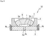
- FIG. 1 is a cross-sectional view of a semiconductor light-emitting device 10.
- FIG. 2 is a plan view of the semiconductor light-emitting device 10 illustrated in FIG. 1 .
- FIG. 3 is a flowchart illustrating the first half of a method for producing the semiconductor light-emitting device 10.
- FIG. 4 is a flowchart illustrating the last half of the method for producing the semiconductor light-emitting device 10.
- the semiconductor light-emitting device 10 includes a metal substrate 2.
- the metal substrate 2 forms a printed circuit board.
- the metal substrate 2 includes an electrode separating groove 3a at the center, and the electrode separating groove 3a receives an electrode separating resin 4a.
- the metal substrate 2 includes a pair of electrodes 2a, 2b each located on different side of the electrode separating groove 3a.
- the pair of electrodes 2a, 2b form an element mounting position 7.
- a semiconductor light-emitting element 1 is flip-chip mounted on the pair of electrodes 2a, 2b.
- a reflector 5 is placed on a main surface of the metal substrate 2, that is, around the element mounting position 7, on which the semiconductor light-emitting element 1 is mounted.
- the reflector 5 receives a light-transmitting resin 6.
- the light-transmitting resin 6 is injected in an internal portion surrounded by the reflector 5 to seal the semiconductor light-emitting element 1.
- the electrode separating resin 4a which has been injected in the electrode separating groove 3a, and a metal substrate holding resin 4b integrate the metal substrate 2 and keep the strength.
- the metal substrate holding resin 4b is injected in a metal substrate holding groove, which will be discussed below.
- the light-transmitting resin 6, which has been injected inside the reflector 5, is a transparent resin or a fluorescent resin.
- a semiconductor light-emitting device that emits white light is formed using a blue LED and a YAG phosphor.
- the blue LED serves as the semiconductor light-emitting element 1.
- the YAG phosphor is used in the fluorescent resin.
- FIG. 3 illustrates production processes (a) to (d).
- the production processes (a) to (d) are the first half of the processes for producing the semiconductor light-emitting device 10.
- FIG. 4 illustrates production processes (e) to (h).
- the production processes (e) to (h) are the last half of the processes for producing the semiconductor light-emitting device 10.
- the production process (a) in FIG. 3 is a groove forming process, and the electrode separating groove 3a and a metal substrate holding groove 3b are formed at a predetermined depth.
- the electrode separating groove 3a is formed at the center portion on the surface of the metal substrate 2.
- the metal substrate holding groove 3b is formed around the element mounting position 7.
- the production process (b) is a resin injecting process.
- the electrode separating resin 4a is injected in the electrode separating groove 3a, and the metal substrate holding resin 4b is injected in the metal substrate holding groove 3b.
- the metal substrate 2 is preferably a copper plate or a copper alloy plate having a thickness of 0.2 mm to 1.0 mm to keep the strength of the substrate although the above-described grooves are formed.
- This embodiment uses a copper plate having a thickness of 0.3 mm.
- the electrode separating resin 4a and the metal substrate holding resin 4b injected in the grooves are preferably, for example, epoxies, silicone resins, and a liquid crystal polymer.
- the production process (c) is an element mounting process.
- the semiconductor light-emitting element 1 is flip-chip mounted on the electrodes 2a, 2b on the surface of the metal substrate 2, which is separated by the electrode separating groove 3a.
- the surface of the metal substrate 2 is kept flat even after the groove forming process and the resin injecting process. This allows the semiconductor light-emitting element 1 to be flip-chip mounted directly on the surface of the metal substrate 2, which includes the electrodes 2a, 2b, without forming bumps on the electrodes of the semiconductor light-emitting device 1 or forming protruding electrodes on the electrodes 2a, 2b of the metal substrate 2.
- protruding electrodes on the electrodes of the semiconductor light-emitting element 1 or on the electrodes 2a, 2b of the metal substrate 2 further improves mounting property.
- wire bonding can also be performed.
- the production process (d) is a reflector forming process.
- the reflector 5 is placed around the semiconductor light-emitting element 1, which is mounted on the element mounting position 7 on the main surface of the metal substrate 2.
- the reflector 5 is made of metal and has a superior reflection property.
- the reflector 5 is bonded to the main surface of the metal substrate 2 with an insulative adhesive.
- the production process (e) in FIG. 4 is a sealing resin injecting process, and the light-transmitting resin 6 such as a transparent resin or a fluorescent resin is injected in the interior of the reflector 5.
- the light-transmitting resin 6 seals the semiconductor light-emitting element 1 and functions to convert the wavelength of light emitted from the semiconductor light-emitting element 1.
- the production process (f) is a grinding process.
- the rear surface of the metal substrate 2 is ground to a position of cutting line T shown by a broken line in FIGs. 4(e) and 4(f) so that the electrode separating resin 4a, which has been injected in the electrode separating groove 3a, is exposed to separate the pair of electrodes 2a, 2b.
- a grinding protective sheet 8a is desirably adhered to the upper surface of the reflector 5, and the metal substrate 2 is desirably mounted on a grinding machine together with the grinding protective sheet 8a. This prevents the semiconductor light-emitting element 1, the reflector 5, and the light-transmitting resin 6, which are mounted on the surface of the metal substrate 2, from being damaged by grinding and polishing the rear surface of the metal substrate 2.
- Injecting the electrode separating resin 4a in the electrode separating groove 3a of the metal substrate 2 and the metal substrate holding resin 4b in the metal substrate holding groove 3b inhibits generation of grinding burrs in the grinding process. That is, since the resins 4a, 4b injected in the grooves 3 a, 3b prevent the grinding burrs from entering the grooves 3a, 3b and cause the burrs to be ground off, the burrs generated in the grinding process are reduced.
- the production process (g) is a cutting and separating process.
- the metal substrate 2 is cut in an area including the semiconductor light-emitting element 1.
- cutting the metal substrate 2 at the position of cutting lines t shown by broken lines, that is, at the center of the metal substrate holding resin 4b completes the semiconductor light-emitting device 10 illustrated in the production process (h).
- the semiconductor light-emitting element 1 is flip-chip mounted on the flat surface of the metal substrate 2 before the rear surface of the metal substrate 2 is ground as described above. The grinding process separates the metal substrate 2 at the pair of electrodes 2a, 2b.
- the electrode separating resin 4a which is applied to the center of the metal substrate 2, the metal substrate holding resin 4b, which is applied to surround the circumference of the metal substrate 2, and the reflector 5, which is secured to the surface of the metal substrate 2, integrate the metal substrate 2 and keep the strength of the metal substrate 2.
- a cutting protective sheet 8b is bonded to the rear surface of the metal substrate 2, and the metal substrate 2 is cut together with the cutting protective sheet 8b.
- FIGs. 5 to 8 illustrate a semiconductor light-emitting device according to a second embodiment of the present invention and a method for producing the semiconductor light-emitting device.
- FIG. 5 is a cross-sectional view of a semiconductor light-emitting device 20
- FIG. 6 is a plan view of the semiconductor light-emitting device 20 illustrated in FIG. 5 .
- FIG. 7 is a flowchart illustrating the first half of the method for producing the semiconductor light-emitting device 20.
- FIG. 8 is a flowchart illustrating the last half of the method for producing the semiconductor light-emitting device 20.
- the semiconductor light-emitting device 20 of this embodiment is approximately the same as the semiconductor light-emitting device 10 described above in the basic configuration except that a reflector forming resin 4c is formed integrally with the metal substrate holding resin 4b, which is provided around the metal substrate 2.
- the reflector forming resin 4c forms the reflector 25.
- Like or the same reference numerals are given to those components that are like or the same as the corresponding components and detailed explanations are omitted.
- FIG. 7 illustrates production processes (a) to (d).
- the production processes (a) to (d) are the first half of the processes for producing the semiconductor light-emitting device 20.
- FIG. 8 illustrates production processes (e) to (g).
- the production processes (e) to (g) are the last half of the processes for producing the semiconductor light-emitting device 20.
- the production process (a) in FIG. 7 is a groove forming process and is the same as the production process (a) in FIG. 3 according to the first embodiment. In the groove forming process, the electrode separating groove 3a and the metal substrate holding groove 3b are formed at a predetermined depth.
- the electrode separating groove 3a is formed at the center portion on the surface of the metal substrate 2.
- the metal substrate holding groove 3b is formed around the element mounting position 7.
- the production process (b) is a resin injecting process.
- the electrode separating resin 4a is injected in the electrode separating groove 3a, and the metal substrate holding resin 4b is injected in the metal substrate holding groove 3b.
- the metal substrate holding resin 4b is formed integrally with the reflector forming resin 4c.
- the reflector forming resin 4c projects from the surface of the metal substrate 2.
- the reflector forming resin 4c has an approximately trapezoidal cross-section having a lower base that is wider than the groove width of the metal substrate holding groove 3b.
- the reflector forming resin 4c has approximately the same height as the reflector 5 of the semiconductor light-emitting device 10 according to the first embodiment and forms the reflector 25.
- the production process (c) is an element mounting process and corresponds to the production process (c) in FIG. 3 according to the first embodiment. That is, the semiconductor light-emitting element 1 is flip-chip mounted on the electrodes 2a, 2b on the surface of the metal substrate 2, which is separated by the electrode separating groove 3a.
- the production process (d) is a sealing resin injecting process and corresponds to the production process (e) in FIG. 4 according to the first embodiment. That is, the semiconductor light-emitting element 1 is sealed by injecting the light-transmitting resin 6 such as a transparent resin or a fluorescent resin inside the reflector 25.
- Cutting line T shown by a broken line indicates the depth by which the rear surface of the metal substrate 2 is ground in the following grinding process.
- the production process (e) in FIG. 8 is a grinding process and corresponds to the production process (f) in FIG. 4 according to the first embodiment.
- the rear surface of the metal substrate 2 is ground to the position of cutting line T shown by a broken line to expose the electrode separating resin 4a, which has been injected in the electrode separating groove 3a.
- the grinding protective sheet 8a is bonded to the upper surface of the reflector forming resin 4c like the first embodiment.
- the production process (f) is a cutting and separating process and corresponds to the production process (g) in FIG. 4 according to the first embodiment.
- the metal substrate 2 is cut in an area including the semiconductor light-emitting element 1.
- cutting the metal substrate 2 at the position of cutting lines t shown by broken lines, that is, at the center of the reflector forming resin 4c and the metal substrate holding resin 4b completes the semiconductor light-emitting device 20 illustrated in the production process (g).
- the reflector forming resin 4c that has been cut forms the reflector 25, which surrounds the element mounting position 7.
- a process for adhering the cutting protective sheet 8b on the rear surface of the metal substrate 2 is provided before the cutting and separating process.
- the semiconductor light-emitting device 20 differs from the semiconductor light-emitting device 10 of the first embodiment in that the reflector 25 is formed simultaneously with the metal substrate holding resin 4b, and the reflector 5 that comes in a separate member is unnecessary. That is, since the reflector 25 is formed integrally with the metal substrate holding resin 4b at the same time, the separate reflector 5 is unnecessary. This also reduces the size. Simultaneously injecting the metal substrate holding resin 4b and the reflector forming resin 4c in the metal substrate holding groove 3b reduces the number of processes and thus reduces the production period and the production costs.
- the resin used in this process is commonly used for the reflector. For this reason, resin including a white resin in which a reflection material such as titanium oxide has been mixed is desirable.
- a silicone resin that includes titanium oxide is used to perform injection molding.
- FIGs. 9 to 12 illustrate semiconductor light-emitting devices according to a third embodiment of the present invention.
- This embodiment employs a collective substrate method that uses a large metal substrate 12 to mass produce the semiconductor light-emitting device 10 of the first embodiment.
- FIG. 9 is a partial plan view of the large metal substrate 12.
- the large metal substrate 12 is preferably a copper plate or a copper alloy plate having a thickness of 0.2 mm to 1.0 mm.
- a copper plate having a length of 78 mm ⁇ 62 mm and a thickness of 0.3 mm is used.
- Multiple reference holes 12a are formed along one side of the copper plate, and alignment holes 12b are formed in the peripheral portion of the copper plate to serve as a position reference in forming the grooves. Since the reference holes 12a and the alignment holes 12b are formed with the same mold during processing of the large metal substrate 12, the position accuracy is high.
- FIG. 10 is a partial plan view of the large metal substrate 12 illustrating a state in which electrode separating grooves 13a and metal substrate holding grooves 13b are formed in the large metal substrate 12. Since the electrode separating grooves 13a and the metal substrate holding grooves 13b are diced with reference to the reference holes 12a, the electrode separating grooves 13a and the metal substrate holding grooves 13b are accurately formed at a predetermined depth. Specifically, the metal substrate holding grooves 13b are formed in the large metal substrate 12 in a checkered pattern. A square area that is defined by the metal substrate holding grooves 13b with the electrode separating groove 13a located at the center corresponds to a configuration area S for forming the individual semiconductor light-emitting device.
- the electrode separating grooves 13a and the metal substrate holding grooves 13b are formed in the large metal substrate 12 at positions specified by the alignment holes 12b in the dicing process. More specifically, a dicing tape is adhered to a surface reverse to the dicing surface of the large metal substrate 12. The large metal substrate 12 is placed in a dicing device together with the dicing tape, and the grooves are formed by dicing. In this case, when the grooves are formed by dicing, metal burrs (dicing burrs) are formed. The dicing burrs that are formed on the upper surface of the large metal substrate 12 particularly raises issues. However, the dicing burrs are removed after dicing by polishing the upper surface of the large metal substrate 12.
- the dicing tape is peeled off to make the large metal substrate 12 in which the electrode separating grooves 13a and the metal substrate holding grooves 13b are formed.
- the metal substrate holding grooves 13b having a groove width of 0.3 mm and a groove depth of 0.15 mm and the electrode separating grooves 13a having a groove width and a groove depth of 0.15 mm are formed.
- the positions of the grooves are determined by the position of electrodes that need to be electrically separated on the semiconductor light-emitting element, the distance between the electrodes, and the size of the semiconductor light-emitting device, which is a base unit, and the grooves are arranged on the large metal substrate 12 in a checkered pattern.
- the metal substrate holding grooves 13b which are formed in the large metal substrate 12, function as separating grooves for separating multiple semiconductor light-emitting devices and separate the multiple semiconductor light-emitting devices formed on the large metal substrate 12.
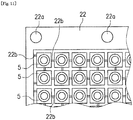
- FIG. 11 is a partial plan view of a large reflector substrate 22.
- the large reflector substrate 22 includes multiple reflectors.
- the large reflector substrate 22 includes reference holes 22a, multiple reflectors 5, and connecting portions 22b.
- the connecting portions 22b connect adjacent reflectors 5 with each other.
- the size and the position of the reflectors 5 correspond to configuration areas S of the semiconductor light-emitting devices, which are formed on the large metal substrate 12.
- the large reflector substrate 22 is preferably a metal plate having a thickness of 0.2 to 3 mm or a substrate having an optical reflection layer formed on the surface of the substrate.
- an aluminum plate having a length of 78 mm ⁇ 62 mm and a thickness of 0.3 mm is used.
- a mass production process for the semiconductor light-emitting device 10 using the large metal substrate 12 and the large reflector substrate 22 will now be described with reference to FIGs. 12 and 13 .
- Processes of the production method using the large metal substrate 12 are basically the same as the production processes (a) to (h) for the semiconductor light-emitting device 10 illustrated in FIGs. 3 and 4 . Description for the production processes (a) to (d) illustrated in FIG. 3 are therefore omitted, and only the production processes (e) to (h) illustrated in FIG. 4 will be described.
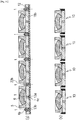
- the production process (e) in FIG. 12 is a sealing resin injecting process. Since FIG. 12 illustrates the groove forming process to the sealing resin injecting process, those processes will be briefly described.
- the electrode separating grooves 13a and the metal substrate holding grooves 13b are formed in the large metal substrate 12 illustrated in FIG. 10 .
- the pole separating resin 4a is injected in the electrode separating grooves 13a, and the metal substrate holding resin 4b is injected in the metal substrate holding grooves 13b.
- the semiconductor light-emitting elements 1 are flip-chip mounted on element mounting positions 17.
- the element mounting positions 17 correspond to the electrode separating grooves 13a of the large metal substrate 12.
- the large reflector substrate 22 illustrated in FIG. 11 is stacked on the large metal substrate 12.
- Stacking of the large reflector substrate 22 on the large metal substrate 12 is performed by aligning the reference holes 12a, 22a, which are formed in the large metal substrate 12 and the large reflector substrate 22.
- the metal substrate holding resin 4b projects from the surface of the large metal substrate 12.
- the reflectors 5 of the large reflector substrate 22 are aligned with the element mounting positions 17 on the large metal substrate 12 when the metal substrate holding resin 4b enters gaps between the reflectors 5 of the large reflector substrate 22.
- the reflectors 5 are accurately positioned with respect to the element mounting positions 17.
- the electrode separating resin 4a and the metal substrate holding resin 4b can be applied by, for example, transferring, injecting, and dropping.
- the resin to be applied includes various kinds of resins such as epoxies, silicone resins, and a liquid crystal polymer.
- the silicone resin is applied by injection.
- the stacking of the large reflector substrate 22 on the large metal substrate 12 will now be described in detail.
- the above-described large metal substrate 12 and the large reflector substrate 22 are stacked by being adhered to each other.
- the material of the reflectors 5 formed on the large reflector substrate 22 may be a metal material such as aluminum and silver, glass, an optical material, or a composite material of these materials. If the reflectors 5 are made of a conductive material, the adhesive needs to keep electrical insulation between the reflectors 5 and the large metal substrate 12. Resins such as an epoxy resin, an acrylic resin, and a silicone resin may be used.
- Those resins have a heat resistance that withstands temperatures greater than or equal to a reflow temperature when the semiconductor light-emitting elements 1 are mounted and a high thixotropy to prevent resin bleed (overflow of resin during adhesion). Furthermore, considering the fact that the semiconductor light-emitting elements 1 are mounted on the large metal substrate 12, a stamping method is suitable as a method for applying the adhesive.
- the adhesive may also be applied by dispensing or in a tape form. In this embodiment, an epoxy adhesive having a high viscosity is applied by stamping.
- the reference holes 12a of the large metal substrate 12 are inserted to positioning pins to secure the large metal substrate 12. Subsequently, an epoxy adhesive layer having a predetermined thickness is formed on a joint surface of the large reflector substrate 22, on which the reflectors 5 are formed, by squeezing. The large reflector substrate 22 is then overlaid on the large metal substrate 12. At this time, the large reflector substrate 22 is adhered to the large metal substrate 12 while the reference holes 22a of the large reflector substrate 22 are inserted to the positioning pins.
- the production process (f) is a grinding process.
- the rear surface of the large metal substrate 12 is ground to the depth of cutting line T shown by a broken line so that the electrode separating resin 4a, which is injected in the electrode separating grooves 13a, is exposed to separate the pairs of electrodes 2a, 2b.
- a large grinding protective sheet 18a is desirably adhered to the upper surfaces of the reflectors 5, and the large metal substrate 12 is desirably mounted on a grinding machine together with the large grinding protective sheet 18a.
- the height of the light-transmitting resins 6 injected in the reflectors 5 is preferably slightly less than the height of the reflectors 5. This is to prevent an adhering surface of the large grinding protective sheet 18 from contacting the upper surfaces of the light-transmitting resins 6 when the large grinding protective sheet 18 is adhered to the upper surfaces of the reflectors 5 as illustrated in the production process (f) in FIG. 12 . Since the upper surfaces of the light-transmitting resins 6 will not be contaminated, the optical property is prevented from deteriorating.
- the production process (g) in FIG. 13 is a cutting and separating process.
- the large metal substrate 12 is cut into areas each including the semiconductor light-emitting element 1.
- multiple semiconductor light-emitting devices 10 are mass produced as illustrated in the production process (h) by cutting the positions of cutting lines t shown by broken lines, that is, at the center of each metal substrate holding resin 4b.
- a process for adhering a large cutting protective sheet 18b to the rear surface of the large metal substrate 12 is provided before the cutting and separating process.
- FIGs. 14 to 17 illustrate a mass production process of semiconductor light-emitting devices according to a fourth embodiment of the present invention.
- This embodiment employs a collective substrate method that uses the large metal substrate 12 to mass produce the semiconductor light-emitting device 20 of the second embodiment.
- the production method of this embodiment is basically the same as the production processes (a) to (g) of the semiconductor light-emitting device 20 described in FIGs. 7 and 8 .
- the description for the production processes (a) to (c) illustrated in FIG. 7 is therefore omitted, and only the production process (d) illustrated in FIG. 7 and the production processes (e) to (g) illustrated in FIG. 8 will be described.
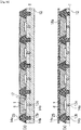
- the production process (d) in FIG. 14 is a sealing resin injecting process. Since FIG. 14 illustrates the groove forming process to the sealing resin injecting process, those processes will be briefly described.
- the electrode separating grooves 13a and the metal substrate holding grooves 13b are formed in the large metal substrate 12 illustrated in FIG. 12 .
- the electrode separating resin 4a is injected in the electrode separating grooves 13a, and the metal substrate holding resin 14b and the reflector forming resin 14c are injected in the metal substrate holding grooves 13b.
- the metal substrate holding resin 14b and the reflector forming resin 14c are combined as a whole.
- the semiconductor light-emitting elements 1 are flip-chip mounted on the element mounting positions 17 corresponding to the electrode separating grooves 13a of the large metal substrate 12.
- Resin is injected in each metal substrate holding groove 13b of the large metal substrate 12.
- Part of the resin embedded in the metal substrate holding groove 13b is the metal substrate holding resin 14b.
- Part of the resin that projects on the surface of the large metal substrate 12 from the metal substrate holding groove 13b is the reflector forming resin 14c.
- the reflector forming resin 14c has an approximately trapezoidal cross-section having a lower base that is wider than the groove width of the metal substrate holding groove 13b.
- the reflector forming resin 14c has a height that is equivalent to the height of the reflector 5 of the semiconductor light-emitting device 10 according to the third embodiment and forms the reflector 25.
- the production process (e) in FIG. 14 is a grinding process and corresponds to the production process (e) in FIG. 8 according to the second embodiment.
- the rear surface of the large metal substrate 12 is ground to the position of cutting line T shown by a broken line so that the electrode separating resin 14a, which is injected in the electrode separating grooves 13a, is exposed to electrically separate the pairs of electrodes 2a, 2b.
- the large grinding protective sheet 18a is desirably adhered to the upper surfaces of the reflectors 25, and the large metal substrate 12 is desirably mounted on a grinding machine together with the large grinding protective sheet 18.
- the height of the light-transmitting resins 6 is preferably slightly less than the height of the above-described reflectors 25.
- the production process (f) in FIG. 15 is a cutting and separating process.
- the large metal substrate 12 is cut into areas each including the semiconductor light-emitting element 1.
- multiple semiconductor light-emitting devices 20 are mass produced as illustrated in the production process (g) by cutting the large metal substrate 12 at the positions of cutting lines t shown by broken lines, that is, at the center of the upper surface of each reflector forming resin 14c.
- a process for adhering the large cutting protective sheet 18b to the rear surface of the large metal substrate 12 is provided before the cutting and separating process.
- the method for producing the semiconductor light-emitting devices 20 according to this embodiment differs from the method for producing the semiconductor light-emitting devices 10 according to the third embodiment in that the reflectors 25 are formed simultaneously with the metal substrate holding resin 14b, and the reflectors 5 that come in separate members are unnecessary. That is, forming the reflectors 25 integrally with the metal substrate holding resin 14b at the same time eliminates the need for the separate reflectors 5 and also reduces the size. Simultaneously injecting the metal substrate holding resin 4b and the reflector forming resin 4c in the metal substrate holding groove 3b further reduces the number of the processes and thus reduces the production period and the production costs.
- FIGs. 16 and 17 illustrate the semiconductor light-emitting devices 20, which have been separated by the cutting and separating process.
- FIG. 16 illustrates the individual semiconductor light-emitting devices 20.
- the individual semiconductor light-emitting devices 20 are obtained by cutting and separating the semiconductor light-emitting elements one by one.
- FIG. 17 illustrates a three-element semiconductor light-emitting device 20.
- the three-element semiconductor light-emitting device 20 is obtained by cutting and separating three semiconductor light-emitting elements as a single semiconductor light-emitting device. It is therefore possible to provide semiconductor light-emitting devices of various sizes desired by customers using the production method of the semiconductor light-emitting device that employs the collective substrate method of the present invention.
- the production method of the semiconductor light-emitting device employing the collective substrate method of the present invention is advantageous in that, after the grinding process (f) of the third embodiment and the grinding process (e) of the fourth embodiment are completed, the optical property and the electrical property of the semiconductor light-emitting devices can be measured with the large protective sheet 18b left adhered to the rear surface of the large metal substrate 12.
- the semiconductor light-emitting devices can be sorted depending on the properties through a batch process.
- FIGs. 18 to 20 illustrate a semiconductor device according to a fifth embodiment of the present invention.
- the semiconductor device according to this embodiment differs from the semiconductor light-emitting devices according to the aforementioned embodiments and is a power control semiconductor device.
- a metal substrate for a printed circuit board of the power control semiconductor device is the same as the metal substrate 2 used in the semiconductor light-emitting device of the first embodiment.
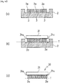
- FIG. 18 is a flowchart illustrating a method for producing a power control semiconductor device 30.
- FIG. 19 is a plan view of the power control semiconductor device 30 made by the production method illustrated in FIG. 18 as viewed from the side of the metal substrate 2 on which the electrodes 2a are provided.
- FIG. 20 is a cross-sectional view of the power control semiconductor device 30 taken along the line A-A of FIG. 19 .
- a power control semiconductor element is a power control semiconductor element 31 in an 80-pin BGA package.
- the production process (a) in FIG. 18 is a groove forming process and is based on the electrode specification for the power control semiconductor element 31.
- the electrode separating grooves 3 are formed in the metal substrate 2 by dicing at intervals of 0.4 mm to conform to the electrode pitch of 0.8 mm and the electrode size of 0.4 mm.
- the electrode separating grooves 3 have a width of 0.30 mm and a depth of 0.15 mm. In this embodiment, ten electrodes 2a are formed in one row.
- the metal substrate 2 is subjected to surface processing to improve mounting property for mounting the power control semiconductor element 31.
- the production process (b) is an element mounting process.
- Lead-free solders are printed on the electrodes 2a of the metal substrate 2, and the power control semiconductor element 31 is placed on the printed lead-free solders.
- the lead-free solders are heated such that the electrodes 2a of the metal substrate 2 and electrodes 31a of the power control semiconductor element 31 are joined by soldering. Welding may be performed instead of soldering.
- the production process (c) is a grinding process.
- the rear surface of the metal substrate 2 is ground and polished to the position of cutting line T shown by a broken line to separate the electrodes 2a. This process completes the power control semiconductor device 30.
- the power control semiconductor device 30 made by the above-described production method has the electrodes 2a including 80 pins arranged in 8 rows and 10 columns on the rear surface as illustrated in FIGs. 19 and 20 .
- this embodiment allows individual radiators, which function also as the electrodes 31a, to be mounted on the power control semiconductor element 31, which includes many electrodes, and further improves heat dissipation using gaps between the electrodes 31a.
- a resin injecting process may be provided after the groove forming process, and an electrode separating resin may be applied to the electrode separating grooves 3.
- the present invention achieves the flatness of the metal substrate without any influence of distortion in the metal substrate that might otherwise be caused during production of the metal substrate or during mounting of the semiconductor element.
- This configuration allows the semiconductor element to be flip-chip mounted at low costs without providing bumps on the semiconductor element and the metal substrate.
- the flip-chip mounting provides high connection reliability.
- the electrodes of the semiconductor device are arranged directly below the electrodes of the semiconductor element, the heat dissipation path is the shortest, and the metal substrate also serves as a heat sink.
- injecting resin in the grooves formed in the metal substrate reduces grinding burrs that might otherwise be caused when grinding the grooves from the rear surface of the metal substrate.
- the resin that projects from the reference holes and the metal substrate serves as a position guide in mounting of the reflectors.
- This configuration improves the position accuracy. Since mounting of the reflectors is performed by a batch process, the production period and the production costs are advantageously reduced. Forming the reflectors on the metal substrate holding grooves (semiconductor device separating grooves) further reduces the size of the semiconductor device. As described above, the present invention provides a semiconductor device that improves the yield and the connection reliability and has good mass productivity and superior heat dissipation efficiency.
- Examples of the present invention include semiconductor light-emitting devices mainly used for lighting, backlight sources of liquid crystal displays, and flush light sources of cameras.
- the present invention is not limited to the semiconductor light-emitting device, but is applicable to mounting of any semiconductor element on a metal substrate.
- the present invention is most suitable for application in power control semiconductor devices.
Landscapes
- Led Device Packages (AREA)
- Encapsulation Of And Coatings For Semiconductor Or Solid State Devices (AREA)
Abstract
Description
- The present invention relates to a semiconductor device that includes a semiconductor element mounted on a metal substrate and to a method for producing the semiconductor device. In particular, the present invention pertains to a semiconductor light-emitting device that includes a metal substrate on which a semiconductor light-emitting element and a reflector are mounted and to a method for producing the semiconductor light-emitting device.
- Light-emitting diodes (LED) have become widely used in lighting devices in recent years. With the increasing use of the LED, demands for improved light-extraction efficiency, improved mass production efficiency, and cost reduction have increased in addition to reduction in the size and the thickness of the LED lighting devices. To reduce the size and the thickness of the devices and increase the light-extraction efficiency, semiconductor light-emitting devices that employ a flip-chip mounting have increased. In the flip-chip mounting, an LED element is directly bonded to a lead frame, which is a kind of metal substrates. Employment of the flip-chip mounting allows electrodes of the LED element to be located on the side facing the lead frame. This eliminates shields on the light radiation surface of the LED element and improves the light-extraction efficiency. Since connection leads of the LED element are formed to overlap the LED element, the size is reduced. Elimination of bonding wires further reduces the thickness.
- The flip-chip mounting on the metal substrate has increased because the metal substrates are lower in cost compared with common resin substrates and because the metal substrates have superior heat dissipation. The semiconductor light-emitting device that employs the flip-chip mounting on the lead frame, however, has a plurality of connection leads arranged apart from each other in the lead frame to connect to the LED element. With this configuration, the difference in the heights between the connection leads, distortions, and warps are issues that need to be solved. The techniques for solving such issues include, as disclosed in
patent document 1, a technique of inserting an electrically insulative reinforcing plate between the connection leads in the lead frame to correct warps. - For semiconductor wafers in other fields, a pre-dicing technique has been proposed to reduce the thickness (patent document 2). The pre-dicing technique includes, first, cutting grooves of a predetermined depth in a semiconductor wafer, backgrinding to allow the grooves to open on the backside, and cutting out semiconductor elements from the semiconductor wafer.
-
- [Patent document 1] Japanese Unexamined Patent Publication No.
2013-157357 FIG. 2 ) - [Patent document 2] Japanese Unexamined Patent Publication No.
11-040520 FIG. 3 ) - As described above, to flip-chip mount the semiconductor element on the metal substrate, strains caused by the difference in the heights of the connection leads, distortions, and warps need to be reduced to increase the yield and the connection reliability. The techniques disclosed in the above-described
patent documents above patent document 1. It is therefore difficult to correct those strains with only a reinforcing member like the reinforcing member disclosed inpatent document 1, and the flatness of the connection leads of the metal substrate required in the flip-chip mounting has not been completely achieved. - Furthermore, as illustrated in
FIG. 2 ofpatent document 1, if the flip-chip mounting is performed without providing conductive protrusions (bumps) on the electrodes of the semiconductor element or projections on the metal substrate, the difference between the heights of the connection leads, distortions, and warps are not absorbed by the height of the bumps, and demand for the flatness of the connection leads is further increased. When the reinforcing member is arranged on the backside of the lead frame, the electrodes of the semiconductor device cannot be arranged directly below the electrodes of the semiconductor element, which undesirably deteriorates heat dissipation. Use of the reinforcing member also increases the number of components and undesirably increases the costs and the number of processes. This results in the increase in the production period. Furthermore, the flow of resin in the following resin molding is hindered. This undesirably decreases the yield. In a case of separating the connection leads by etching also, the internal strain, the thermal stress, and the heat dissipation of the metal substrate are the same as those in the case of pressing. In addition, etching has low mass productivity and undesirably increases costs. - The problem of the strains in the metal substrate is caused by separating the connection leads of the metal substrate when flip-chip mounting the semiconductor element. The inventors considered applying the pre-dicing technique disclosed in
patent document 2 to the metal substrate not for the purpose of preventing chipping of the semiconductor wafer during dicing, but for the purpose of reducing the strains in the connection leads caused by separating the connection leads. In this case, the metal substrate differs from the semiconductor wafer in that the material itself has workability in rolling. For this reason, when the metal substrate is ground and polished, metal burrs are generated in addition to the strains in the connection leads. As a result, the yield is undesirably reduced. - To solve the above-described problems, it is an object of the present invention to provide a method for producing a semiconductor device that improves yield and connection reliability, has good mass productivity, and in which a semiconductor element is flip-chip mounted on a metal substrate, which has excellent heat dissipation, and to provide the semiconductor device at low costs.
- To achieve the above object, in a semiconductor device including a metal substrate including a pair of electrodes and a semiconductor element configured to be mounted on the metal substrate and sealed with resin, a method for producing a semiconductor device according to one aspect of the present invention includes forming an electrode separating groove in an element mounting position on a main surface of the metal substrate at a predetermined depth. The semiconductor element is mounted to extend over the electrode separating groove. The metal substrate is ground from a surface reverse to the main surface of the metal substrate up to a position reaching the electrode separating groove.
- With the above-described production method, since the semiconductor element is mounted on the metal substrate before cutting and separating connection leads formed of the metal substrate, mounting of the semiconductor element is completed before strains occur in processing of the metal substrate. That is, when the semiconductor element is mounted, the main surface of the metal substrate is kept flat, and the semiconductor element is allowed to be flip-chip mounted without forming bumps on the electrodes of the semiconductor element.
- The first aspect of the present invention may further include injecting resin in the electrode separating groove.
- In the first aspect of the present invention, the groove forming step may include forming a metal substrate holding groove around the element mounting position together with the electrode separating groove, and the resin injecting step may include injecting a metal substrate holding resin in the metal substrate holding groove.
- Injecting the resin in the groove inhibits generation of grinding burrs in the following process for grinding and polishing the metal substrate to a predetermined depth from the surface reverse to the main surface of the metal substrate. The resin that fills the groove prevents the grinding burrs from entering the groove and causes the grinding burrs to be ground off. Thus, the metal burrs generated during grinding or polishing are reduced. Furthermore, since no strain is generated during metalworking, the main surface of the metal substrate is kept flat. This allows the electrodes to be directly adhered to each other without providing bumps on the semiconductor element or on the metal substrate.
- The first aspect of the present invention may further include forming a reflector around the semiconductor element, which is mounted on the element mounting position on the main surface of the metal substrate.
- In the first aspect of the present invention, the reflector forming step may include forming the reflector with the metal substrate holding resin, which is injected in the metal substrate holding groove.
- The first aspect of the present invention may further include injecting a light-transmitting resin in the reflector to seal the semiconductor element.
- According to another aspect of the present invention, in a semiconductor device including a metal substrate including a pair of electrodes and a semiconductor element configured to be mounted on the metal substrate and sealed with resin, a method for producing semiconductor devices includes the following four steps: (1) forming electrode separating grooves in a plurality of element mounting positions on a main surface of a large metal substrate at a predetermined depth, (2) mounting semiconductor elements each extending over the associated electrode separating groove, (3) grinding the metal substrate from a surface reverse to the main surface of the metal substrate up to a position reaching the electrode separating grooves, and (4) cutting the large metal substrate in areas each including the semiconductor element mounted on the associated element mounting position to separate into semiconductor devices.
- Another aspect of the present invention may further include injecting resin in the electrode separating grooves.
- In another aspect of the present invention, the groove forming step may include forming metal substrate holding grooves around the element mounting positions together with the electrode separating grooves, and the resin injecting step may include injecting a metal substrate holding resin in the metal substrate holding grooves.
- With the above-described production method, the semiconductor devices having desired properties are easily mass produced using the large metal substrate. That is, the semiconductor devices are mass produced very efficiently by simultaneously forming the electrode separating grooves and the metal substrate holding grooves in the large metal substrate, simultaneously injecting the resin in the grooves, and simultaneously grinding the rear surface of the large metal substrate.
- Another aspect of the present invention may further include forming reflectors around the semiconductor elements, which are mounted on the element mounting positions on the main surface of the large metal substrate.
- In another aspect of the present invention, the reflector forming step may include stacking a reflector large substrate comprising a plurality of reflector portions corresponding to the element mounting positions on the main surface of the large metal substrate.
- In another aspect of the present invention, the reflector forming step may include forming the reflectors with the metal substrate holding resin, which is injected in the metal substrate holding grooves.
- Another aspect of the present invention may include adhering a grinding protective sheet to the surface of the elements on the main surface of the large metal substrate prior to the grinding step.
- Damages on the semiconductor elements or components are reduced during grinding of the rear surface of the large metal substrate by adhering the protective sheet for grinding or polishing on the side of the large metal substrate on which the semiconductor elements are mounted as described above.
- In another aspect of the present invention, the cutting and separating step may include cutting the large metal substrate at a position of the metal substrate holding resin.
- Another aspect of the present invention may include adhering a cutting protective sheet on the rear surface of the large metal substrate prior to the cutting and separating step.
- Damages on the semiconductor elements or components are reduced during an element separating process by adhering the cutting protective sheet on the rear surface of the large metal substrate as described above.
- The semiconductor device produced by the above production method may be a single-element semiconductor device in which elements are cut and separated one each, or a multi-element semiconductor device in which multiple elements are cut and separated as one unit.
- According to the present invention, since the semiconductor element is mounted on the metal substrate before cutting and separating the connection leads formed of the metal substrate, mounting of the semiconductor element is completed before strains occur in processing of the metal substrate. That is, when the semiconductor element is mounted, the main surface of the metal substrate is kept flat, and the semiconductor element is allowed to be flip-chip mounted without forming bumps on the electrodes of the semiconductor element.
-
-
FIG. 1 is a cross-sectional view of a semiconductor light-emitting device according to a first embodiment of the present invention; -
FIG. 2 is a plan view of the semiconductor light-emitting device illustrated inFIG. 1 ; -
FIG. 3 is a flowchart illustrating the first half of a method for producing the semiconductor light-emitting device illustrated inFIG. 1 ; -
FIG. 4 is a flowchart illustrating the last half of the method for producing the semiconductor light-emitting device illustrated inFIG. 1 ; -
FIG. 5 is a cross-sectional view of a semiconductor light-emitting device according to a second embodiment of the present invention; -
FIG. 6 is a plan view of the semiconductor light-emitting device illustrated inFIG. 5 ; -
FIG. 7 is a flowchart illustrating the first half of a method for producing the semiconductor light-emitting device illustrated inFIG. 5 ; -
FIG. 8 is a flowchart illustrating the last half of the method for producing the semiconductor light-emitting device illustrated inFIG. 5 ; -
FIG. 9 is a partial plan view of a large metal substrate used for semiconductor light-emitting devices according to a third embodiment of the present invention; -
FIG. 10 is a partial plan view of the large metal substrate showing a state in which electrode separating grooves and metal substrate holding grooves are formed in the large metal substrate illustrated inFIG. 9 ; -
FIG. 11 is a partial plan view of a large reflector substrate used in the semiconductor light-emitting devices according to the third embodiment of the present invention; -
FIG. 12 is a flowchart illustrating the first half of a method for producing the semiconductor light-emitting devices according to the third embodiment of the present invention; -
FIG. 13 is a flowchart illustrating the last half of the process for producing the semiconductor light-emitting devices according to the third embodiment of the present invention; -
FIG. 14 is a flowchart illustrating the first half of a method for producing semiconductor light-emitting devices according to a fourth embodiment of the present invention; -
FIG. 15 is a flowchart illustrating the last half of the method for producing the semiconductor light-emitting devices according to the fourth embodiment of the present invention; -
FIG. 16 is a cross-sectional view of semiconductor light-emitting devices cut and separated one each; -
FIG. 17 is a cross-sectional view of a semiconductor light-emitting device cut and separated as one semiconductor light-emitting device including three semiconductor light-emitting elements; -
FIG. 18 is a flowchart illustrating a method for producing a power control semiconductor device according to a fifth embodiment of the present invention; -
FIG. 19 is a plan view of the power control semiconductor device produced by the method ofFIG. 18 as viewed from the side on which the electrodes are provided; and -
FIG. 20 is a cross-sectional view of the power control semiconductor device taken along the line A-A ofFIG. 19 . - A semiconductor light-emitting device according to an embodiment of the present invention and a method for producing the semiconductor light-emitting device will hereafter be described with reference to the drawings. Semiconductor light-emitting devices are widely used among semiconductor devices. A semiconductor light-emitting element is therefore described as an example of a semiconductor element mounted on a semiconductor light-emitting device. In each of embodiments, like or the same reference numerals are given to those components that are like or the same as the corresponding components and redundant explanations are omitted.
-
FIGs. 1 to 4 illustrate a semiconductor light-emitting device according to a first embodiment of the present invention.FIG. 1 is a cross-sectional view of a semiconductor light-emittingdevice 10.FIG. 2 is a plan view of the semiconductor light-emittingdevice 10 illustrated inFIG. 1 .FIG. 3 is a flowchart illustrating the first half of a method for producing the semiconductor light-emittingdevice 10.FIG. 4 is a flowchart illustrating the last half of the method for producing the semiconductor light-emittingdevice 10. - As illustrated in
FIGs. 1 and2 , the semiconductor light-emittingdevice 10 includes ametal substrate 2. Themetal substrate 2 forms a printed circuit board. Themetal substrate 2 includes anelectrode separating groove 3a at the center, and theelectrode separating groove 3a receives anelectrode separating resin 4a. Themetal substrate 2 includes a pair ofelectrodes electrode separating groove 3a. The pair ofelectrodes element mounting position 7. A semiconductor light-emittingelement 1 is flip-chip mounted on the pair ofelectrodes reflector 5 is placed on a main surface of themetal substrate 2, that is, around theelement mounting position 7, on which the semiconductor light-emittingelement 1 is mounted. Thereflector 5 receives a light-transmittingresin 6. The light-transmittingresin 6 is injected in an internal portion surrounded by thereflector 5 to seal the semiconductor light-emittingelement 1. - The
electrode separating resin 4a, which has been injected in theelectrode separating groove 3a, and a metalsubstrate holding resin 4b integrate themetal substrate 2 and keep the strength. The metalsubstrate holding resin 4b is injected in a metal substrate holding groove, which will be discussed below. The light-transmittingresin 6, which has been injected inside thereflector 5, is a transparent resin or a fluorescent resin. As an example, a semiconductor light-emitting device that emits white light is formed using a blue LED and a YAG phosphor. The blue LED serves as the semiconductor light-emittingelement 1. The YAG phosphor is used in the fluorescent resin. - Next, a method for producing the above-described semiconductor light-emitting
device 10 will be described with reference toFIGs. 3 and4 .FIG. 3 illustrates production processes (a) to (d). The production processes (a) to (d) are the first half of the processes for producing the semiconductor light-emittingdevice 10.FIG. 4 illustrates production processes (e) to (h). The production processes (e) to (h) are the last half of the processes for producing the semiconductor light-emittingdevice 10. The production process (a) inFIG. 3 is a groove forming process, and theelectrode separating groove 3a and a metalsubstrate holding groove 3b are formed at a predetermined depth. Theelectrode separating groove 3a is formed at the center portion on the surface of themetal substrate 2. The metalsubstrate holding groove 3b is formed around theelement mounting position 7. The production process (b) is a resin injecting process. Theelectrode separating resin 4a is injected in theelectrode separating groove 3a, and the metalsubstrate holding resin 4b is injected in the metalsubstrate holding groove 3b. - The
metal substrate 2 is preferably a copper plate or a copper alloy plate having a thickness of 0.2 mm to 1.0 mm to keep the strength of the substrate although the above-described grooves are formed. This embodiment uses a copper plate having a thickness of 0.3 mm. Theelectrode separating resin 4a and the metalsubstrate holding resin 4b injected in the grooves are preferably, for example, epoxies, silicone resins, and a liquid crystal polymer. - The production process (c) is an element mounting process. The semiconductor light-emitting
element 1 is flip-chip mounted on theelectrodes metal substrate 2, which is separated by theelectrode separating groove 3a. The surface of themetal substrate 2 is kept flat even after the groove forming process and the resin injecting process. This allows the semiconductor light-emittingelement 1 to be flip-chip mounted directly on the surface of themetal substrate 2, which includes theelectrodes device 1 or forming protruding electrodes on theelectrodes metal substrate 2. As a matter of course, forming protruding electrodes on the electrodes of the semiconductor light-emittingelement 1 or on theelectrodes metal substrate 2 further improves mounting property. Depending on the structure of the semiconductor light-emitting element, wire bonding can also be performed. - The production process (d) is a reflector forming process. The
reflector 5 is placed around the semiconductor light-emittingelement 1, which is mounted on theelement mounting position 7 on the main surface of themetal substrate 2. In this embodiment, thereflector 5 is made of metal and has a superior reflection property. Thereflector 5 is bonded to the main surface of themetal substrate 2 with an insulative adhesive. - The production process (e) in
FIG. 4 is a sealing resin injecting process, and the light-transmittingresin 6 such as a transparent resin or a fluorescent resin is injected in the interior of thereflector 5. The light-transmittingresin 6 seals the semiconductor light-emittingelement 1 and functions to convert the wavelength of light emitted from the semiconductor light-emittingelement 1. - The production process (f) is a grinding process. The rear surface of the
metal substrate 2 is ground to a position of cutting line T shown by a broken line inFIGs. 4(e) and 4(f) so that theelectrode separating resin 4a, which has been injected in theelectrode separating groove 3a, is exposed to separate the pair ofelectrodes protective sheet 8a is desirably adhered to the upper surface of thereflector 5, and themetal substrate 2 is desirably mounted on a grinding machine together with the grindingprotective sheet 8a. This prevents the semiconductor light-emittingelement 1, thereflector 5, and the light-transmittingresin 6, which are mounted on the surface of themetal substrate 2, from being damaged by grinding and polishing the rear surface of themetal substrate 2. - Injecting the
electrode separating resin 4a in theelectrode separating groove 3a of themetal substrate 2 and the metalsubstrate holding resin 4b in the metalsubstrate holding groove 3b inhibits generation of grinding burrs in the grinding process. That is, since theresins grooves grooves - The production process (g) is a cutting and separating process. The
metal substrate 2 is cut in an area including the semiconductor light-emittingelement 1. In this embodiment, cutting themetal substrate 2 at the position of cutting lines t shown by broken lines, that is, at the center of the metalsubstrate holding resin 4b completes the semiconductor light-emittingdevice 10 illustrated in the production process (h). In the semiconductor light-emittingdevice 10, the semiconductor light-emittingelement 1 is flip-chip mounted on the flat surface of themetal substrate 2 before the rear surface of themetal substrate 2 is ground as described above. The grinding process separates themetal substrate 2 at the pair ofelectrodes electrode separating resin 4a, which is applied to the center of themetal substrate 2, the metalsubstrate holding resin 4b, which is applied to surround the circumference of themetal substrate 2, and thereflector 5, which is secured to the surface of themetal substrate 2, integrate themetal substrate 2 and keep the strength of themetal substrate 2. Before the cutting and separating process, a cuttingprotective sheet 8b is bonded to the rear surface of themetal substrate 2, and themetal substrate 2 is cut together with the cuttingprotective sheet 8b. -
FIGs. 5 to 8 illustrate a semiconductor light-emitting device according to a second embodiment of the present invention and a method for producing the semiconductor light-emitting device.FIG. 5 is a cross-sectional view of a semiconductor light-emittingdevice 20, andFIG. 6 is a plan view of the semiconductor light-emittingdevice 20 illustrated inFIG. 5 .FIG. 7 is a flowchart illustrating the first half of the method for producing the semiconductor light-emittingdevice 20.FIG. 8 is a flowchart illustrating the last half of the method for producing the semiconductor light-emittingdevice 20. - The semiconductor light-emitting
device 20 of this embodiment is approximately the same as the semiconductor light-emittingdevice 10 described above in the basic configuration except that areflector forming resin 4c is formed integrally with the metalsubstrate holding resin 4b, which is provided around themetal substrate 2. Thereflector forming resin 4c forms thereflector 25. Like or the same reference numerals are given to those components that are like or the same as the corresponding components and detailed explanations are omitted. - A method for producing the above-described semiconductor light-emitting
device 20 will now be described with reference toFIGs. 7 and8 .FIG. 7 illustrates production processes (a) to (d). The production processes (a) to (d) are the first half of the processes for producing the semiconductor light-emittingdevice 20.FIG. 8 illustrates production processes (e) to (g). The production processes (e) to (g) are the last half of the processes for producing the semiconductor light-emittingdevice 20. The production process (a) inFIG. 7 is a groove forming process and is the same as the production process (a) inFIG. 3 according to the first embodiment. In the groove forming process, theelectrode separating groove 3a and the metalsubstrate holding groove 3b are formed at a predetermined depth. Theelectrode separating groove 3a is formed at the center portion on the surface of themetal substrate 2. The metalsubstrate holding groove 3b is formed around theelement mounting position 7. The production process (b) is a resin injecting process. Theelectrode separating resin 4a is injected in theelectrode separating groove 3a, and the metalsubstrate holding resin 4b is injected in the metalsubstrate holding groove 3b. The metalsubstrate holding resin 4b is formed integrally with thereflector forming resin 4c. Thereflector forming resin 4c projects from the surface of themetal substrate 2. - The
reflector forming resin 4c has an approximately trapezoidal cross-section having a lower base that is wider than the groove width of the metalsubstrate holding groove 3b. Thereflector forming resin 4c has approximately the same height as thereflector 5 of the semiconductor light-emittingdevice 10 according to the first embodiment and forms thereflector 25. - The production process (c) is an element mounting process and corresponds to the production process (c) in
FIG. 3 according to the first embodiment. That is, the semiconductor light-emittingelement 1 is flip-chip mounted on theelectrodes metal substrate 2, which is separated by theelectrode separating groove 3a. - The production process (d) is a sealing resin injecting process and corresponds to the production process (e) in
FIG. 4 according to the first embodiment. That is, the semiconductor light-emittingelement 1 is sealed by injecting the light-transmittingresin 6 such as a transparent resin or a fluorescent resin inside thereflector 25. Cutting line T shown by a broken line indicates the depth by which the rear surface of themetal substrate 2 is ground in the following grinding process. - The production process (e) in
FIG. 8 is a grinding process and corresponds to the production process (f) inFIG. 4 according to the first embodiment. As described above, the rear surface of themetal substrate 2 is ground to the position of cutting line T shown by a broken line to expose theelectrode separating resin 4a, which has been injected in theelectrode separating groove 3a. In the grinding process, the grindingprotective sheet 8a is bonded to the upper surface of thereflector forming resin 4c like the first embodiment. - The production process (f) is a cutting and separating process and corresponds to the production process (g) in
FIG. 4 according to the first embodiment. Themetal substrate 2 is cut in an area including the semiconductor light-emittingelement 1. In this embodiment, cutting themetal substrate 2 at the position of cutting lines t shown by broken lines, that is, at the center of thereflector forming resin 4c and the metalsubstrate holding resin 4b completes the semiconductor light-emittingdevice 20 illustrated in the production process (g). Thereflector forming resin 4c that has been cut forms thereflector 25, which surrounds theelement mounting position 7. Like the first embodiment, a process for adhering the cuttingprotective sheet 8b on the rear surface of themetal substrate 2 is provided before the cutting and separating process. - The semiconductor light-emitting
device 20 according to this embodiment differs from the semiconductor light-emittingdevice 10 of the first embodiment in that thereflector 25 is formed simultaneously with the metalsubstrate holding resin 4b, and thereflector 5 that comes in a separate member is unnecessary. That is, since thereflector 25 is formed integrally with the metalsubstrate holding resin 4b at the same time, theseparate reflector 5 is unnecessary. This also reduces the size. Simultaneously injecting the metalsubstrate holding resin 4b and thereflector forming resin 4c in the metalsubstrate holding groove 3b reduces the number of processes and thus reduces the production period and the production costs. The resin used in this process is commonly used for the reflector. For this reason, resin including a white resin in which a reflection material such as titanium oxide has been mixed is desirable. In this embodiment, a silicone resin that includes titanium oxide is used to perform injection molding. -
FIGs. 9 to 12 illustrate semiconductor light-emitting devices according to a third embodiment of the present invention. This embodiment employs a collective substrate method that uses alarge metal substrate 12 to mass produce the semiconductor light-emittingdevice 10 of the first embodiment. -
FIG. 9 is a partial plan view of thelarge metal substrate 12. Since the substrate strength needs to be maintained although the grooves are formed in the substrate, thelarge metal substrate 12 is preferably a copper plate or a copper alloy plate having a thickness of 0.2 mm to 1.0 mm. In this embodiment, a copper plate having a length of 78 mm × 62 mm and a thickness of 0.3 mm is used.Multiple reference holes 12a are formed along one side of the copper plate, andalignment holes 12b are formed in the peripheral portion of the copper plate to serve as a position reference in forming the grooves. Since thereference holes 12a and the alignment holes 12b are formed with the same mold during processing of thelarge metal substrate 12, the position accuracy is high. -
FIG. 10 is a partial plan view of thelarge metal substrate 12 illustrating a state in which electrode separatinggrooves 13a and metalsubstrate holding grooves 13b are formed in thelarge metal substrate 12. Since theelectrode separating grooves 13a and the metalsubstrate holding grooves 13b are diced with reference to thereference holes 12a, theelectrode separating grooves 13a and the metalsubstrate holding grooves 13b are accurately formed at a predetermined depth. Specifically, the metalsubstrate holding grooves 13b are formed in thelarge metal substrate 12 in a checkered pattern. A square area that is defined by the metalsubstrate holding grooves 13b with theelectrode separating groove 13a located at the center corresponds to a configuration area S for forming the individual semiconductor light-emitting device. - As described above, in this embodiment, the
electrode separating grooves 13a and the metalsubstrate holding grooves 13b are formed in thelarge metal substrate 12 at positions specified by the alignment holes 12b in the dicing process. More specifically, a dicing tape is adhered to a surface reverse to the dicing surface of thelarge metal substrate 12. Thelarge metal substrate 12 is placed in a dicing device together with the dicing tape, and the grooves are formed by dicing. In this case, when the grooves are formed by dicing, metal burrs (dicing burrs) are formed. The dicing burrs that are formed on the upper surface of thelarge metal substrate 12 particularly raises issues. However, the dicing burrs are removed after dicing by polishing the upper surface of thelarge metal substrate 12. - After the dicing burrs are removed, the dicing tape is peeled off to make the
large metal substrate 12 in which theelectrode separating grooves 13a and the metalsubstrate holding grooves 13b are formed. In this embodiment, the metalsubstrate holding grooves 13b having a groove width of 0.3 mm and a groove depth of 0.15 mm and theelectrode separating grooves 13a having a groove width and a groove depth of 0.15 mm are formed. The positions of the grooves are determined by the position of electrodes that need to be electrically separated on the semiconductor light-emitting element, the distance between the electrodes, and the size of the semiconductor light-emitting device, which is a base unit, and the grooves are arranged on thelarge metal substrate 12 in a checkered pattern. In this embodiment, the case in which the grooves are formed by dicing is described. However, the grooves can certainly be made by other machining methods such as pressing. The metalsubstrate holding grooves 13b, which are formed in thelarge metal substrate 12, function as separating grooves for separating multiple semiconductor light-emitting devices and separate the multiple semiconductor light-emitting devices formed on thelarge metal substrate 12. -
FIG. 11 is a partial plan view of alarge reflector substrate 22. Thelarge reflector substrate 22 includes multiple reflectors. Thelarge reflector substrate 22 includesreference holes 22a,multiple reflectors 5, and connectingportions 22b. The connectingportions 22b connectadjacent reflectors 5 with each other. The size and the position of thereflectors 5 correspond to configuration areas S of the semiconductor light-emitting devices, which are formed on thelarge metal substrate 12. Since thereflectors 5 form reflection surfaces, thelarge reflector substrate 22 is preferably a metal plate having a thickness of 0.2 to 3 mm or a substrate having an optical reflection layer formed on the surface of the substrate. In this embodiment, an aluminum plate having a length of 78 mm × 62 mm and a thickness of 0.3 mm is used. - A mass production process for the semiconductor light-emitting
device 10 using thelarge metal substrate 12 and thelarge reflector substrate 22 will now be described with reference toFIGs. 12 and13 . Processes of the production method using thelarge metal substrate 12 are basically the same as the production processes (a) to (h) for the semiconductor light-emittingdevice 10 illustrated inFIGs. 3 and4 . Description for the production processes (a) to (d) illustrated inFIG. 3 are therefore omitted, and only the production processes (e) to (h) illustrated inFIG. 4 will be described. - The production process (e) in
FIG. 12 is a sealing resin injecting process. SinceFIG. 12 illustrates the groove forming process to the sealing resin injecting process, those processes will be briefly described. First, theelectrode separating grooves 13a and the metalsubstrate holding grooves 13b are formed in thelarge metal substrate 12 illustrated inFIG. 10 . Thepole separating resin 4a is injected in theelectrode separating grooves 13a, and the metalsubstrate holding resin 4b is injected in the metalsubstrate holding grooves 13b. Subsequently, the semiconductor light-emittingelements 1 are flip-chip mounted on element mounting positions 17. Theelement mounting positions 17 correspond to theelectrode separating grooves 13a of thelarge metal substrate 12. - Next, the
large reflector substrate 22 illustrated inFIG. 11 is stacked on thelarge metal substrate 12. Stacking of thelarge reflector substrate 22 on thelarge metal substrate 12 is performed by aligning thereference holes large metal substrate 12 and thelarge reflector substrate 22. The metalsubstrate holding resin 4b projects from the surface of thelarge metal substrate 12. Thereflectors 5 of thelarge reflector substrate 22 are aligned with theelement mounting positions 17 on thelarge metal substrate 12 when the metalsubstrate holding resin 4b enters gaps between thereflectors 5 of thelarge reflector substrate 22. Thus, thereflectors 5 are accurately positioned with respect to the element mounting positions 17. Part of the metalsubstrate holding resin 4b on thelarge metal substrate 12 that corresponds to the connectingportions 22b, which connect thereflectors 5 of thelarge reflector substrate 22, in other words, a metal substrate holding resin 4b'does not project from the surface of thelarge metal substrate 12. This configuration allows thelarge reflector substrate 22 to be stacked on thelarge metal substrate 12. Subsequently, the light-transmittingresin 6 is injected inside thereflectors 5, which are provided on thelarge metal substrate 12, to seal the semiconductor light-emittingelements 1. This completes the sealing resin injecting process of the production process (e). - The
electrode separating resin 4a and the metalsubstrate holding resin 4b can be applied by, for example, transferring, injecting, and dropping. The resin to be applied includes various kinds of resins such as epoxies, silicone resins, and a liquid crystal polymer. In this embodiment, the silicone resin is applied by injection. - The stacking of the
large reflector substrate 22 on thelarge metal substrate 12 will now be described in detail. The above-describedlarge metal substrate 12 and thelarge reflector substrate 22 are stacked by being adhered to each other. The material of thereflectors 5 formed on thelarge reflector substrate 22 may be a metal material such as aluminum and silver, glass, an optical material, or a composite material of these materials. If thereflectors 5 are made of a conductive material, the adhesive needs to keep electrical insulation between thereflectors 5 and thelarge metal substrate 12. Resins such as an epoxy resin, an acrylic resin, and a silicone resin may be used. Those resins have a heat resistance that withstands temperatures greater than or equal to a reflow temperature when the semiconductor light-emittingelements 1 are mounted and a high thixotropy to prevent resin bleed (overflow of resin during adhesion). Furthermore, considering the fact that the semiconductor light-emittingelements 1 are mounted on thelarge metal substrate 12, a stamping method is suitable as a method for applying the adhesive. The adhesive may also be applied by dispensing or in a tape form. In this embodiment, an epoxy adhesive having a high viscosity is applied by stamping. - To stack the
large reflector substrate 22 on thelarge metal substrate 12, first, thereference holes 12a of thelarge metal substrate 12 are inserted to positioning pins to secure thelarge metal substrate 12. Subsequently, an epoxy adhesive layer having a predetermined thickness is formed on a joint surface of thelarge reflector substrate 22, on which thereflectors 5 are formed, by squeezing. Thelarge reflector substrate 22 is then overlaid on thelarge metal substrate 12. At this time, thelarge reflector substrate 22 is adhered to thelarge metal substrate 12 while thereference holes 22a of thelarge reflector substrate 22 are inserted to the positioning pins. Even if there is a displacement in the position accuracy of thereflectors 5 formed on thelarge reflector substrate 22, the position is corrected by the metalsubstrate holding resin 4b, which projects from thelarge metal substrate 12. Thus, the final position accuracy is improved. Subsequently, the adhesive is cured by a heating process so that thereflectors 5 are secured to thelarge metal substrate 12. As a result, light emitted from the side surfaces of each semiconductor light-emittingelement 1 is reflected upward by the associatedreflector 5. This configuration improves the light-extraction efficiency. - The production process (f) is a grinding process. The rear surface of the
large metal substrate 12 is ground to the depth of cutting line T shown by a broken line so that theelectrode separating resin 4a, which is injected in theelectrode separating grooves 13a, is exposed to separate the pairs ofelectrodes elements 1, thereflectors 5, and the light-transmittingresins 6, which are mounted on the surface of thelarge metal substrate 12, from being damaged by grinding and polishing the rear surface of thelarge metal substrate 12, a large grindingprotective sheet 18a is desirably adhered to the upper surfaces of thereflectors 5, and thelarge metal substrate 12 is desirably mounted on a grinding machine together with the large grindingprotective sheet 18a. - The height of the light-transmitting
resins 6 injected in thereflectors 5 is preferably slightly less than the height of thereflectors 5. This is to prevent an adhering surface of the large grinding protective sheet 18 from contacting the upper surfaces of the light-transmittingresins 6 when the large grinding protective sheet 18 is adhered to the upper surfaces of thereflectors 5 as illustrated in the production process (f) inFIG. 12 . Since the upper surfaces of the light-transmittingresins 6 will not be contaminated, the optical property is prevented from deteriorating. - The production process (g) in
FIG. 13 is a cutting and separating process. Thelarge metal substrate 12 is cut into areas each including the semiconductor light-emittingelement 1. In this embodiment, multiple semiconductor light-emittingdevices 10 are mass produced as illustrated in the production process (h) by cutting the positions of cutting lines t shown by broken lines, that is, at the center of each metalsubstrate holding resin 4b. A process for adhering a large cuttingprotective sheet 18b to the rear surface of thelarge metal substrate 12 is provided before the cutting and separating process. -
FIGs. 14 to 17 illustrate a mass production process of semiconductor light-emitting devices according to a fourth embodiment of the present invention. This embodiment employs a collective substrate method that uses thelarge metal substrate 12 to mass produce the semiconductor light-emittingdevice 20 of the second embodiment. - The production method of this embodiment is basically the same as the production processes (a) to (g) of the semiconductor light-emitting
device 20 described inFIGs. 7 and8 . The description for the production processes (a) to (c) illustrated inFIG. 7 is therefore omitted, and only the production process (d) illustrated inFIG. 7 and the production processes (e) to (g) illustrated inFIG. 8 will be described. - The production process (d) in
FIG. 14 is a sealing resin injecting process. SinceFIG. 14 illustrates the groove forming process to the sealing resin injecting process, those processes will be briefly described. First, theelectrode separating grooves 13a and the metalsubstrate holding grooves 13b are formed in thelarge metal substrate 12 illustrated inFIG. 12 . Theelectrode separating resin 4a is injected in theelectrode separating grooves 13a, and the metalsubstrate holding resin 14b and thereflector forming resin 14c are injected in the metalsubstrate holding grooves 13b. The metalsubstrate holding resin 14b and thereflector forming resin 14c are combined as a whole. Subsequently, the semiconductor light-emittingelements 1 are flip-chip mounted on theelement mounting positions 17 corresponding to theelectrode separating grooves 13a of thelarge metal substrate 12. - Resin is injected in each metal
substrate holding groove 13b of thelarge metal substrate 12. Part of the resin embedded in the metalsubstrate holding groove 13b is the metalsubstrate holding resin 14b. Part of the resin that projects on the surface of thelarge metal substrate 12 from the metalsubstrate holding groove 13b is thereflector forming resin 14c. Thereflector forming resin 14c has an approximately trapezoidal cross-section having a lower base that is wider than the groove width of the metalsubstrate holding groove 13b. Thereflector forming resin 14c has a height that is equivalent to the height of thereflector 5 of the semiconductor light-emittingdevice 10 according to the third embodiment and forms thereflector 25. - The production process (e) in
FIG. 14 is a grinding process and corresponds to the production process (e) inFIG. 8 according to the second embodiment. The rear surface of thelarge metal substrate 12 is ground to the position of cutting line T shown by a broken line so that theelectrode separating resin 14a, which is injected in theelectrode separating grooves 13a, is exposed to electrically separate the pairs ofelectrodes elements 1, thereflectors 25, and the light-transmittingresins 6, which are mounted on the surface of thelarge metal substrate 12, from being damaged by grinding and polishing the rear surface of thelarge metal substrate 12, the large grindingprotective sheet 18a is desirably adhered to the upper surfaces of thereflectors 25, and thelarge metal substrate 12 is desirably mounted on a grinding machine together with the large grinding protective sheet 18. The height of the light-transmittingresins 6 is preferably slightly less than the height of the above-describedreflectors 25. - The production process (f) in
FIG. 15 is a cutting and separating process. Thelarge metal substrate 12 is cut into areas each including the semiconductor light-emittingelement 1. In this embodiment, multiple semiconductor light-emittingdevices 20 are mass produced as illustrated in the production process (g) by cutting thelarge metal substrate 12 at the positions of cutting lines t shown by broken lines, that is, at the center of the upper surface of eachreflector forming resin 14c. A process for adhering the large cuttingprotective sheet 18b to the rear surface of thelarge metal substrate 12 is provided before the cutting and separating process. - The method for producing the semiconductor light-emitting
devices 20 according to this embodiment differs from the method for producing the semiconductor light-emittingdevices 10 according to the third embodiment in that thereflectors 25 are formed simultaneously with the metalsubstrate holding resin 14b, and thereflectors 5 that come in separate members are unnecessary. That is, forming thereflectors 25 integrally with the metalsubstrate holding resin 14b at the same time eliminates the need for theseparate reflectors 5 and also reduces the size. Simultaneously injecting the metalsubstrate holding resin 4b and thereflector forming resin 4c in the metalsubstrate holding groove 3b further reduces the number of the processes and thus reduces the production period and the production costs. -
FIGs. 16 and17 illustrate the semiconductor light-emittingdevices 20, which have been separated by the cutting and separating process.FIG. 16 illustrates the individual semiconductor light-emittingdevices 20. The individual semiconductor light-emittingdevices 20 are obtained by cutting and separating the semiconductor light-emitting elements one by one.FIG. 17 illustrates a three-element semiconductor light-emittingdevice 20. The three-element semiconductor light-emittingdevice 20 is obtained by cutting and separating three semiconductor light-emitting elements as a single semiconductor light-emitting device. It is therefore possible to provide semiconductor light-emitting devices of various sizes desired by customers using the production method of the semiconductor light-emitting device that employs the collective substrate method of the present invention. - The production method of the semiconductor light-emitting device employing the collective substrate method of the present invention is advantageous in that, after the grinding process (f) of the third embodiment and the grinding process (e) of the fourth embodiment are completed, the optical property and the electrical property of the semiconductor light-emitting devices can be measured with the large
protective sheet 18b left adhered to the rear surface of thelarge metal substrate 12. The semiconductor light-emitting devices can be sorted depending on the properties through a batch process. -
FIGs. 18 to 20 illustrate a semiconductor device according to a fifth embodiment of the present invention. The semiconductor device according to this embodiment differs from the semiconductor light-emitting devices according to the aforementioned embodiments and is a power control semiconductor device. A metal substrate for a printed circuit board of the power control semiconductor device is the same as themetal substrate 2 used in the semiconductor light-emitting device of the first embodiment. -
FIG. 18 is a flowchart illustrating a method for producing a powercontrol semiconductor device 30.FIG. 19 is a plan view of the powercontrol semiconductor device 30 made by the production method illustrated inFIG. 18 as viewed from the side of themetal substrate 2 on which theelectrodes 2a are provided.FIG. 20 is a cross-sectional view of the powercontrol semiconductor device 30 taken along the line A-A ofFIG. 19 . In this embodiment, a power control semiconductor element is a powercontrol semiconductor element 31 in an 80-pin BGA package. - The production process (a) in
FIG. 18 is a groove forming process and is based on the electrode specification for the powercontrol semiconductor element 31. Theelectrode separating grooves 3 are formed in themetal substrate 2 by dicing at intervals of 0.4 mm to conform to the electrode pitch of 0.8 mm and the electrode size of 0.4 mm. Theelectrode separating grooves 3 have a width of 0.30 mm and a depth of 0.15 mm. In this embodiment, tenelectrodes 2a are formed in one row. Themetal substrate 2 is subjected to surface processing to improve mounting property for mounting the powercontrol semiconductor element 31. - The production process (b) is an element mounting process. Lead-free solders are printed on the
electrodes 2a of themetal substrate 2, and the powercontrol semiconductor element 31 is placed on the printed lead-free solders. The lead-free solders are heated such that theelectrodes 2a of themetal substrate 2 andelectrodes 31a of the powercontrol semiconductor element 31 are joined by soldering. Welding may be performed instead of soldering. - The production process (c) is a grinding process. The rear surface of the
metal substrate 2 is ground and polished to the position of cutting line T shown by a broken line to separate theelectrodes 2a. This process completes the powercontrol semiconductor device 30. - The power
control semiconductor device 30 made by the above-described production method has theelectrodes 2a including 80 pins arranged in 8 rows and 10 columns on the rear surface as illustrated inFIGs. 19 and 20 . - As described above, this embodiment allows individual radiators, which function also as the
electrodes 31a, to be mounted on the powercontrol semiconductor element 31, which includes many electrodes, and further improves heat dissipation using gaps between theelectrodes 31a. Although omitted in this embodiment, a resin injecting process may be provided after the groove forming process, and an electrode separating resin may be applied to theelectrode separating grooves 3. - As described above, with the pre-dicing process performed on the metal substrate, the present invention achieves the flatness of the metal substrate without any influence of distortion in the metal substrate that might otherwise be caused during production of the metal substrate or during mounting of the semiconductor element. This configuration allows the semiconductor element to be flip-chip mounted at low costs without providing bumps on the semiconductor element and the metal substrate. The flip-chip mounting provides high connection reliability. Furthermore, since the electrodes of the semiconductor device are arranged directly below the electrodes of the semiconductor element, the heat dissipation path is the shortest, and the metal substrate also serves as a heat sink. Thus, the semiconductor device that has high heat dissipation efficiency and high reliability is provided. Moreover, injecting resin in the grooves formed in the metal substrate reduces grinding burrs that might otherwise be caused when grinding the grooves from the rear surface of the metal substrate.
- In addition, when the reflectors are mounted, the resin that projects from the reference holes and the metal substrate serves as a position guide in mounting of the reflectors. This configuration improves the position accuracy. Since mounting of the reflectors is performed by a batch process, the production period and the production costs are advantageously reduced. Forming the reflectors on the metal substrate holding grooves (semiconductor device separating grooves) further reduces the size of the semiconductor device. As described above, the present invention provides a semiconductor device that improves the yield and the connection reliability and has good mass productivity and superior heat dissipation efficiency.
- Examples of the present invention include semiconductor light-emitting devices mainly used for lighting, backlight sources of liquid crystal displays, and flush light sources of cameras. The present invention is not limited to the semiconductor light-emitting device, but is applicable to mounting of any semiconductor element on a metal substrate. In particular, with superior heat dissipation efficiency, the present invention is most suitable for application in power control semiconductor devices.
-
- 1
- semiconductor light-emitting element (semiconductor element)
- 2
- metal substrate
- 2a, 2b
- electrode
- 3, 3a, 13a
- electrode separating groove
- 3b, 13b
- metal substrate holding groove
- 4a, 14a
- electrode separating resin
- 4b, 14b
- metal substrate holding resin
- 14c
- reflector forming resin
- 5,25
- reflector
- 6
- light-transmitting resin
- 7, 17
- element mounting position
- 8a
- grinding protective sheet
- 8b
- cutting protective sheet
- 18a
- large grinding protective sheet
- 18b
- large cutting protective sheet
- 10, 20
- semiconductor light-emitting device (semiconductor device)
- 12
- large metal substrate
- 12a, 22a
- reference hole
- 12b
- alignment hole
- 22
- large reflector substrate
- 22b
- connecting portion
- 30
- power control semiconductor device
- 31
- power control semiconductor element
- 31a
- electrode
- S
- configuration area
- T, t
- cutting line
Claims (18)
- A method for producing a semiconductor device comprising:a metal substrate comprising a pair of electrodes; anda semiconductor element configured to be mounted on the metal substrate and sealed with resin,the method comprising:forming an electrode separating groove in an element mounting position on a main surface of the metal substrate at a predetermined depth;mounting the semiconductor element to extend over the electrode separating groove; andgrinding the metal substrate from a surface reverse to the main surface of the metal substrate up to a position reaching the electrode separating groove.
- The method for producing a semiconductor device according to claim 1, further comprising injecting resin in the electrode separating groove.
- The method for producing a semiconductor device according to claim 2, wherein the resin injecting step comprises injecting a metal substrate holding resin in a metal substrate holding groove formed around the element mounting position.
- The method for producing a semiconductor device according to any one of claims 1 to 3, further comprising forming a reflector around the semiconductor element, which is mounted on the element mounting position on the main surface of the metal substrate.
- The method for producing a semiconductor device according to claim 4, wherein the reflector forming step comprises forming the reflector with the metal substrate holding resin, which is injected in the metal substrate holding groove.
- The method for producing a semiconductor device according to claim 4 or 5, further comprising injecting a light-transmitting resin in the reflector to seal the semiconductor element.
- A method for producing semiconductor devices, each semiconductor device comprising:a metal substrate comprising a pair of electrodes; anda semiconductor element configured to be mounted on the metal substrate and sealed with resin,the method comprising:forming electrode separating grooves in a plurality of element mounting positions on a main surface of a large metal substrate at a predetermined depth;mounting semiconductor elements, each extending over the associated electrode separating groove;grinding the metal substrate from a surface reverse to the main surface of the metal substrate up to a position reaching the electrode separating grooves; andcutting the large metal substrate in areas each including the semiconductor element mounted on the associated element mounting position to separate into semiconductor devices.
- The method for producing semiconductor devices according to claim 7, further comprising injecting resin in the electrode separating grooves.
- The method for producing semiconductor devices according to claim 8, wherein the resin injecting step comprises injecting a metal substrate holding resin in metal substrate holding grooves formed around the element mounting positions.
- The method for producing semiconductor devices according to any one of claims 7 to 9, further comprising forming reflectors around the semiconductor elements, which are mounted on the element mounting positions on the main surface of the large metal substrate.
- The method for producing semiconductor devices according to claim 10, wherein the reflector forming step comprises stacking a reflector large substrate comprising a plurality of reflector portions corresponding to the element mounting positions on the main surface of the large metal substrate.
- The method for producing semiconductor devices according to claim 10, wherein the reflector forming step comprises forming the reflectors with the metal substrate holding resin, which is injected in the metal substrate holding grooves.
- The method for producing semiconductor devices according to any one of claims 10 to 12, further comprising injecting a light-transmitting resin in the reflectors to seal the semiconductor elements.
- The method for producing semiconductor devices according to any one of claims 7 to 12, further comprising adhering a grinding protective sheet to the surface of the elements on the main surface of the large metal substrate prior to the grinding step.
- The method for producing semiconductor devices according to any one of claims 7 to 13, wherein the cutting and separating step comprises cutting the large metal substrate at predetermined positions of the metal substrate holding resin.
- The method for producing semiconductor devices according to any one of claims 7 to 14, further comprising adhering a cutting protective sheet on the rear surface of the large metal substrate prior to the cutting and separating step.
- A semiconductor device comprising being manufactured by the production method according to claims 1 to 15.
- A semiconductor device comprising a plurality of semiconductor elements produced by the production method according to claims 7 to 15.
Applications Claiming Priority (2)
| Application Number | Priority Date | Filing Date | Title |
|---|---|---|---|
| JP2014159333 | 2014-08-05 | ||
| PCT/JP2015/071607 WO2016021476A1 (en) | 2014-08-05 | 2015-07-30 | Semiconductor device and method for manufacturing same |
Publications (3)
| Publication Number | Publication Date |
|---|---|
| EP3179525A4 EP3179525A4 (en) | 2017-06-14 |
| EP3179525A1 true EP3179525A1 (en) | 2017-06-14 |
| EP3179525B1 EP3179525B1 (en) | 2018-10-24 |
Family
ID=55263745
Family Applications (1)
| Application Number | Title | Priority Date | Filing Date |
|---|---|---|---|
| EP15830533.4A Not-in-force EP3179525B1 (en) | 2014-08-05 | 2015-07-30 | Semiconductor device and method for producing same |
Country Status (5)
| Country | Link |
|---|---|
| US (1) | US10181553B2 (en) |
| EP (1) | EP3179525B1 (en) |
| JP (1) | JP6126752B2 (en) |
| CN (1) | CN106663731B (en) |
| WO (1) | WO2016021476A1 (en) |
Cited By (2)
| Publication number | Priority date | Publication date | Assignee | Title |
|---|---|---|---|---|
| US20220231208A1 (en) * | 2021-01-20 | 2022-07-21 | Chang Wah Technology Co., Ltd. | Composite lead frame and light-emitting diode package structure including the same |
| WO2024042049A1 (en) * | 2022-08-25 | 2024-02-29 | Ams-Osram International Gmbh | Radiation-emitting semiconductor component and method for producing radiation-emitting semiconductor components |
Families Citing this family (10)
| Publication number | Priority date | Publication date | Assignee | Title |
|---|---|---|---|---|
| JP6888296B2 (en) * | 2016-12-26 | 2021-06-16 | 日亜化学工業株式会社 | Manufacturing method of light emitting device |
| JP6579141B2 (en) * | 2017-03-24 | 2019-09-25 | 日亜化学工業株式会社 | Light emitting device and method for manufacturing light emitting device |
| US11329030B2 (en) | 2017-05-02 | 2022-05-10 | Osram Opto Semiconductors Gmbh | Production of a chip module |
| KR102641336B1 (en) * | 2017-09-05 | 2024-02-28 | 쑤저우 레킨 세미컨덕터 컴퍼니 리미티드 | Semiconductor device package |
| DE102017128457A1 (en) * | 2017-11-30 | 2019-06-06 | Osram Opto Semiconductors Gmbh | MANUFACTURE OF OPTOELECTRONIC COMPONENTS |
| JP6974724B2 (en) * | 2018-03-08 | 2021-12-01 | 日亜化学工業株式会社 | Manufacturing method of light emitting device |
| JP7218126B2 (en) * | 2018-08-30 | 2023-02-06 | キヤノン株式会社 | Units, modules and devices with circuit boards |
| JP7186358B2 (en) * | 2018-11-15 | 2022-12-09 | 日亜化学工業株式会社 | Method for manufacturing light emitting device, light emitting device and light source device |
| JP7406314B2 (en) * | 2019-06-24 | 2023-12-27 | キヤノン株式会社 | electronic modules and equipment |
| KR102625710B1 (en) | 2021-09-24 | 2024-01-16 | 주식회사 루츠 | A manufacturing method of a fluorescent substance |
Family Cites Families (19)
| Publication number | Priority date | Publication date | Assignee | Title |
|---|---|---|---|---|
| JPH07106285A (en) * | 1993-10-08 | 1995-04-21 | Oki Electric Ind Co Ltd | Semiconductor manufacturing method |
| JPH1140520A (en) | 1997-07-23 | 1999-02-12 | Toshiba Corp | Method of dividing wafer and method of manufacturing semiconductor device |
| US6294439B1 (en) | 1997-07-23 | 2001-09-25 | Kabushiki Kaisha Toshiba | Method of dividing a wafer and method of manufacturing a semiconductor device |
| US6184109B1 (en) | 1997-07-23 | 2001-02-06 | Kabushiki Kaisha Toshiba | Method of dividing a wafer and method of manufacturing a semiconductor device |
| US6599768B1 (en) * | 2002-08-20 | 2003-07-29 | United Epitaxy Co., Ltd. | Surface mounting method for high power light emitting diode |
| TW563263B (en) * | 2002-09-27 | 2003-11-21 | United Epitaxy Co Ltd | Surface mounting method for high power light emitting diode |
| CN201054360Y (en) | 2007-02-28 | 2008-04-30 | 深圳市丽晶光电科技有限公司 | LED part with pasting and welding surface |
| JP2011025347A (en) | 2009-07-24 | 2011-02-10 | Disco Abrasive Syst Ltd | Method for machining metal plate |
| CN103190008B (en) | 2010-11-02 | 2016-07-06 | 大日本印刷株式会社 | Lead frame for mounting LED element, lead frame with resin, manufacturing method of semiconductor device, and lead frame for mounting semiconductor element |
| CN103392242B (en) | 2011-02-28 | 2017-02-22 | 日亚化学工业株式会社 | Light emitting device |
| JP5693313B2 (en) | 2011-03-23 | 2015-04-01 | シチズン電子株式会社 | Manufacturing method of semiconductor light emitting device using lead frame |
| CN202111151U (en) | 2011-05-13 | 2012-01-11 | 佛山市国星光电股份有限公司 | Novel TOP LED support and TOP LED device manufactured by using the same |
| JP5720496B2 (en) | 2011-08-24 | 2015-05-20 | 豊田合成株式会社 | Light emitting device and manufacturing method thereof |
| US8324082B1 (en) | 2011-09-15 | 2012-12-04 | SemiLEDs Optoelectronics Co., Ltd. | Method for fabricating conductive substrates for electronic and optoelectronic devices |
| CN108155142B (en) * | 2011-09-30 | 2022-05-03 | 琳得科株式会社 | Dicing film having protective film forming layer and method for manufacturing chip |
| KR20130081949A (en) * | 2012-01-10 | 2013-07-18 | 삼성전자주식회사 | Method for dicing wafer and method for manufacturing light emitting device chips using the same |
| JP6078948B2 (en) * | 2012-01-20 | 2017-02-15 | 日亜化学工業株式会社 | Package molded body for light emitting device and light emitting device using the same |
| JP5978631B2 (en) | 2012-01-26 | 2016-08-24 | 日亜化学工業株式会社 | Light emitting device |
| CN202917534U (en) | 2012-10-19 | 2013-05-01 | 博罗承创精密工业有限公司 | LED bracket and terminal material belt structure thereof |
-
2015
- 2015-07-30 US US15/501,577 patent/US10181553B2/en active Active
- 2015-07-30 JP JP2016540181A patent/JP6126752B2/en active Active
- 2015-07-30 CN CN201580041468.8A patent/CN106663731B/en not_active Expired - Fee Related
- 2015-07-30 WO PCT/JP2015/071607 patent/WO2016021476A1/en not_active Ceased
- 2015-07-30 EP EP15830533.4A patent/EP3179525B1/en not_active Not-in-force
Cited By (2)
| Publication number | Priority date | Publication date | Assignee | Title |
|---|---|---|---|---|
| US20220231208A1 (en) * | 2021-01-20 | 2022-07-21 | Chang Wah Technology Co., Ltd. | Composite lead frame and light-emitting diode package structure including the same |
| WO2024042049A1 (en) * | 2022-08-25 | 2024-02-29 | Ams-Osram International Gmbh | Radiation-emitting semiconductor component and method for producing radiation-emitting semiconductor components |
Also Published As
| Publication number | Publication date |
|---|---|
| EP3179525B1 (en) | 2018-10-24 |
| WO2016021476A1 (en) | 2016-02-11 |
| CN106663731B (en) | 2019-08-06 |
| JPWO2016021476A1 (en) | 2017-05-25 |
| EP3179525A4 (en) | 2017-06-14 |
| CN106663731A (en) | 2017-05-10 |
| US10181553B2 (en) | 2019-01-15 |
| JP6126752B2 (en) | 2017-05-10 |
| US20180175267A1 (en) | 2018-06-21 |
Similar Documents
| Publication | Publication Date | Title |
|---|---|---|
| EP3179525B1 (en) | Semiconductor device and method for producing same | |
| CN104094426B (en) | Semiconductor light emitting device and manufacturing method thereof | |
| US9269873B2 (en) | Semiconductor light emitting device and method for manufacturing same | |
| EP3261136B1 (en) | Light-emitting device and method for producing the same | |
| EP2383808B1 (en) | Light emitting device package having leads with a recess for the chip mount area, and corresponding manufacturing methods | |
| CN101930934B (en) | Method for manufacturing light emitting apparatus, light emitting apparatus, and mounting base thereof | |
| EP2590215B1 (en) | Substrate, light emitting device and method for manufacturing substrate | |
| US20140138725A1 (en) | Semiconductor light-emitting device and producing method thereof | |
| CN102347424A (en) | Semiconductor device, lead frame assembly, and method for fabricating same | |
| US20130307014A1 (en) | Semiconductor light emitting device | |
| US12002907B2 (en) | Light emitting module and method for manufacturing same | |
| TWI497773B (en) | Film wiring substrate and light emitting device | |
| CN1347153A (en) | Semiconductor device and mehtod for mfg. same | |
| US10707389B2 (en) | Light emitting device | |
| US20120015463A1 (en) | Method for manufacturing light-emitting device | |
| JP2012164902A (en) | Method of manufacturing semiconductor light-emitting device | |
| JP2014003102A (en) | Method for manufacturing light emitting device | |
| JP6680274B2 (en) | Light emitting device and lead frame with resin | |
| US10714360B2 (en) | Method for manufacturing a module and an optical module | |
| US9252090B2 (en) | Resin package | |
| CN107068668B (en) | Semiconductor device with a plurality of semiconductor chips | |
| JP2017005247A (en) | Method for manufacturing light-emitting device, and light-emitting device | |
| CN102782876A (en) | Solar cell assembly I | |
| JPH11307816A (en) | Package structure for chip semiconductor and its manufacture | |
| CN119677261A (en) | Package structure |
Legal Events
| Date | Code | Title | Description |
|---|---|---|---|
| STAA | Information on the status of an ep patent application or granted ep patent |
Free format text: STATUS: THE INTERNATIONAL PUBLICATION HAS BEEN MADE |
|
| PUAI | Public reference made under article 153(3) epc to a published international application that has entered the european phase |
Free format text: ORIGINAL CODE: 0009012 |
|
| STAA | Information on the status of an ep patent application or granted ep patent |
Free format text: STATUS: REQUEST FOR EXAMINATION WAS MADE |
|
| 17P | Request for examination filed |
Effective date: 20170306 |
|
| A4 | Supplementary search report drawn up and despatched |
Effective date: 20170419 |
|
| AK | Designated contracting states |
Kind code of ref document: A1 Designated state(s): AL AT BE BG CH CY CZ DE DK EE ES FI FR GB GR HR HU IE IS IT LI LT LU LV MC MK MT NL NO PL PT RO RS SE SI SK SM TR |
|
| AX | Request for extension of the european patent |
Extension state: BA ME |
|
| DAV | Request for validation of the european patent (deleted) | ||
| DAX | Request for extension of the european patent (deleted) | ||
| GRAP | Despatch of communication of intention to grant a patent |
Free format text: ORIGINAL CODE: EPIDOSNIGR1 |
|
| STAA | Information on the status of an ep patent application or granted ep patent |
Free format text: STATUS: GRANT OF PATENT IS INTENDED |
|
| INTG | Intention to grant announced |
Effective date: 20180329 |
|
| GRAS | Grant fee paid |
Free format text: ORIGINAL CODE: EPIDOSNIGR3 |
|
| GRAJ | Information related to disapproval of communication of intention to grant by the applicant or resumption of examination proceedings by the epo deleted |
Free format text: ORIGINAL CODE: EPIDOSDIGR1 |
|
| GRAL | Information related to payment of fee for publishing/printing deleted |
Free format text: ORIGINAL CODE: EPIDOSDIGR3 |
|
| STAA | Information on the status of an ep patent application or granted ep patent |
Free format text: STATUS: REQUEST FOR EXAMINATION WAS MADE |
|
| REG | Reference to a national code |
Ref country code: DE Ref legal event code: R079 Ref document number: 602015018880 Country of ref document: DE Free format text: PREVIOUS MAIN CLASS: H01L0033620000 Ipc: H01L0023120000 |
|
| GRAR | Information related to intention to grant a patent recorded |
Free format text: ORIGINAL CODE: EPIDOSNIGR71 |
|
| STAA | Information on the status of an ep patent application or granted ep patent |
Free format text: STATUS: GRANT OF PATENT IS INTENDED |
|
| INTC | Intention to grant announced (deleted) | ||
| GRAA | (expected) grant |
Free format text: ORIGINAL CODE: 0009210 |
|
| STAA | Information on the status of an ep patent application or granted ep patent |
Free format text: STATUS: THE PATENT HAS BEEN GRANTED |
|
| AK | Designated contracting states |
Kind code of ref document: B1 Designated state(s): AL AT BE BG CH CY CZ DE DK EE ES FI FR GB GR HR HU IE IS IT LI LT LU LV MC MK MT NL NO PL PT RO RS SE SI SK SM TR |
|
| INTG | Intention to grant announced |
Effective date: 20180914 |
|
| RIC1 | Information provided on ipc code assigned before grant |
Ipc: H01L 23/00 20060101ALI20180914BHEP Ipc: H01L 33/00 20100101ALN20180914BHEP Ipc: H01L 33/56 20100101ALN20180914BHEP Ipc: H01L 33/62 20100101ALN20180914BHEP Ipc: H01L 33/60 20100101ALN20180914BHEP Ipc: H01L 23/12 20060101AFI20180914BHEP Ipc: H01L 33/48 20100101ALI20180914BHEP |
|
| REG | Reference to a national code |
Ref country code: CH Ref legal event code: EP |
|
| REG | Reference to a national code |
Ref country code: IE Ref legal event code: FG4D |
|
| REG | Reference to a national code |
Ref country code: AT Ref legal event code: REF Ref document number: 1057689 Country of ref document: AT Kind code of ref document: T Effective date: 20181115 |
|
| REG | Reference to a national code |
Ref country code: DE Ref legal event code: R096 Ref document number: 602015018880 Country of ref document: DE |
|
| REG | Reference to a national code |
Ref country code: NL Ref legal event code: MP Effective date: 20181024 |
|
| REG | Reference to a national code |
Ref country code: LT Ref legal event code: MG4D |
|
| REG | Reference to a national code |
Ref country code: AT Ref legal event code: MK05 Ref document number: 1057689 Country of ref document: AT Kind code of ref document: T Effective date: 20181024 |
|
| PG25 | Lapsed in a contracting state [announced via postgrant information from national office to epo] |
Ref country code: NL Free format text: LAPSE BECAUSE OF FAILURE TO SUBMIT A TRANSLATION OF THE DESCRIPTION OR TO PAY THE FEE WITHIN THE PRESCRIBED TIME-LIMIT Effective date: 20181024 |
|
| PG25 | Lapsed in a contracting state [announced via postgrant information from national office to epo] |
Ref country code: LV Free format text: LAPSE BECAUSE OF FAILURE TO SUBMIT A TRANSLATION OF THE DESCRIPTION OR TO PAY THE FEE WITHIN THE PRESCRIBED TIME-LIMIT Effective date: 20181024 Ref country code: FI Free format text: LAPSE BECAUSE OF FAILURE TO SUBMIT A TRANSLATION OF THE DESCRIPTION OR TO PAY THE FEE WITHIN THE PRESCRIBED TIME-LIMIT Effective date: 20181024 Ref country code: BG Free format text: LAPSE BECAUSE OF FAILURE TO SUBMIT A TRANSLATION OF THE DESCRIPTION OR TO PAY THE FEE WITHIN THE PRESCRIBED TIME-LIMIT Effective date: 20190124 Ref country code: NO Free format text: LAPSE BECAUSE OF FAILURE TO SUBMIT A TRANSLATION OF THE DESCRIPTION OR TO PAY THE FEE WITHIN THE PRESCRIBED TIME-LIMIT Effective date: 20190124 Ref country code: PL Free format text: LAPSE BECAUSE OF FAILURE TO SUBMIT A TRANSLATION OF THE DESCRIPTION OR TO PAY THE FEE WITHIN THE PRESCRIBED TIME-LIMIT Effective date: 20181024 Ref country code: AT Free format text: LAPSE BECAUSE OF FAILURE TO SUBMIT A TRANSLATION OF THE DESCRIPTION OR TO PAY THE FEE WITHIN THE PRESCRIBED TIME-LIMIT Effective date: 20181024 Ref country code: HR Free format text: LAPSE BECAUSE OF FAILURE TO SUBMIT A TRANSLATION OF THE DESCRIPTION OR TO PAY THE FEE WITHIN THE PRESCRIBED TIME-LIMIT Effective date: 20181024 Ref country code: LT Free format text: LAPSE BECAUSE OF FAILURE TO SUBMIT A TRANSLATION OF THE DESCRIPTION OR TO PAY THE FEE WITHIN THE PRESCRIBED TIME-LIMIT Effective date: 20181024 Ref country code: ES Free format text: LAPSE BECAUSE OF FAILURE TO SUBMIT A TRANSLATION OF THE DESCRIPTION OR TO PAY THE FEE WITHIN THE PRESCRIBED TIME-LIMIT Effective date: 20181024 Ref country code: IS Free format text: LAPSE BECAUSE OF FAILURE TO SUBMIT A TRANSLATION OF THE DESCRIPTION OR TO PAY THE FEE WITHIN THE PRESCRIBED TIME-LIMIT Effective date: 20190224 |
|
| PG25 | Lapsed in a contracting state [announced via postgrant information from national office to epo] |
Ref country code: SE Free format text: LAPSE BECAUSE OF FAILURE TO SUBMIT A TRANSLATION OF THE DESCRIPTION OR TO PAY THE FEE WITHIN THE PRESCRIBED TIME-LIMIT Effective date: 20181024 Ref country code: RS Free format text: LAPSE BECAUSE OF FAILURE TO SUBMIT A TRANSLATION OF THE DESCRIPTION OR TO PAY THE FEE WITHIN THE PRESCRIBED TIME-LIMIT Effective date: 20181024 Ref country code: PT Free format text: LAPSE BECAUSE OF FAILURE TO SUBMIT A TRANSLATION OF THE DESCRIPTION OR TO PAY THE FEE WITHIN THE PRESCRIBED TIME-LIMIT Effective date: 20190224 Ref country code: GR Free format text: LAPSE BECAUSE OF FAILURE TO SUBMIT A TRANSLATION OF THE DESCRIPTION OR TO PAY THE FEE WITHIN THE PRESCRIBED TIME-LIMIT Effective date: 20190125 Ref country code: AL Free format text: LAPSE BECAUSE OF FAILURE TO SUBMIT A TRANSLATION OF THE DESCRIPTION OR TO PAY THE FEE WITHIN THE PRESCRIBED TIME-LIMIT Effective date: 20181024 |
|
| REG | Reference to a national code |
Ref country code: DE Ref legal event code: R097 Ref document number: 602015018880 Country of ref document: DE |
|
| PG25 | Lapsed in a contracting state [announced via postgrant information from national office to epo] |
Ref country code: CZ Free format text: LAPSE BECAUSE OF FAILURE TO SUBMIT A TRANSLATION OF THE DESCRIPTION OR TO PAY THE FEE WITHIN THE PRESCRIBED TIME-LIMIT Effective date: 20181024 Ref country code: IT Free format text: LAPSE BECAUSE OF FAILURE TO SUBMIT A TRANSLATION OF THE DESCRIPTION OR TO PAY THE FEE WITHIN THE PRESCRIBED TIME-LIMIT Effective date: 20181024 Ref country code: DK Free format text: LAPSE BECAUSE OF FAILURE TO SUBMIT A TRANSLATION OF THE DESCRIPTION OR TO PAY THE FEE WITHIN THE PRESCRIBED TIME-LIMIT Effective date: 20181024 |
|
| PG25 | Lapsed in a contracting state [announced via postgrant information from national office to epo] |
Ref country code: SK Free format text: LAPSE BECAUSE OF FAILURE TO SUBMIT A TRANSLATION OF THE DESCRIPTION OR TO PAY THE FEE WITHIN THE PRESCRIBED TIME-LIMIT Effective date: 20181024 Ref country code: SM Free format text: LAPSE BECAUSE OF FAILURE TO SUBMIT A TRANSLATION OF THE DESCRIPTION OR TO PAY THE FEE WITHIN THE PRESCRIBED TIME-LIMIT Effective date: 20181024 Ref country code: EE Free format text: LAPSE BECAUSE OF FAILURE TO SUBMIT A TRANSLATION OF THE DESCRIPTION OR TO PAY THE FEE WITHIN THE PRESCRIBED TIME-LIMIT Effective date: 20181024 Ref country code: RO Free format text: LAPSE BECAUSE OF FAILURE TO SUBMIT A TRANSLATION OF THE DESCRIPTION OR TO PAY THE FEE WITHIN THE PRESCRIBED TIME-LIMIT Effective date: 20181024 |
|
| PLBE | No opposition filed within time limit |
Free format text: ORIGINAL CODE: 0009261 |
|
| STAA | Information on the status of an ep patent application or granted ep patent |
Free format text: STATUS: NO OPPOSITION FILED WITHIN TIME LIMIT |
|
| 26N | No opposition filed |
Effective date: 20190725 |
|
| PG25 | Lapsed in a contracting state [announced via postgrant information from national office to epo] |
Ref country code: SI Free format text: LAPSE BECAUSE OF FAILURE TO SUBMIT A TRANSLATION OF THE DESCRIPTION OR TO PAY THE FEE WITHIN THE PRESCRIBED TIME-LIMIT Effective date: 20181024 |
|
| PGFP | Annual fee paid to national office [announced via postgrant information from national office to epo] |
Ref country code: DE Payment date: 20190517 Year of fee payment: 5 |
|
| PG25 | Lapsed in a contracting state [announced via postgrant information from national office to epo] |
Ref country code: MC Free format text: LAPSE BECAUSE OF FAILURE TO SUBMIT A TRANSLATION OF THE DESCRIPTION OR TO PAY THE FEE WITHIN THE PRESCRIBED TIME-LIMIT Effective date: 20181024 |
|
| REG | Reference to a national code |
Ref country code: CH Ref legal event code: PL |
|
| GBPC | Gb: european patent ceased through non-payment of renewal fee |
Effective date: 20190730 |
|
| PG25 | Lapsed in a contracting state [announced via postgrant information from national office to epo] |
Ref country code: TR Free format text: LAPSE BECAUSE OF FAILURE TO SUBMIT A TRANSLATION OF THE DESCRIPTION OR TO PAY THE FEE WITHIN THE PRESCRIBED TIME-LIMIT Effective date: 20181024 |
|
| REG | Reference to a national code |
Ref country code: BE Ref legal event code: MM Effective date: 20190731 |
|
| PG25 | Lapsed in a contracting state [announced via postgrant information from national office to epo] |
Ref country code: GB Free format text: LAPSE BECAUSE OF NON-PAYMENT OF DUE FEES Effective date: 20190730 |
|
| PG25 | Lapsed in a contracting state [announced via postgrant information from national office to epo] |
Ref country code: BE Free format text: LAPSE BECAUSE OF NON-PAYMENT OF DUE FEES Effective date: 20190731 Ref country code: CH Free format text: LAPSE BECAUSE OF NON-PAYMENT OF DUE FEES Effective date: 20190731 Ref country code: LU Free format text: LAPSE BECAUSE OF NON-PAYMENT OF DUE FEES Effective date: 20190730 Ref country code: LI Free format text: LAPSE BECAUSE OF NON-PAYMENT OF DUE FEES Effective date: 20190731 |
|
| PG25 | Lapsed in a contracting state [announced via postgrant information from national office to epo] |
Ref country code: FR Free format text: LAPSE BECAUSE OF NON-PAYMENT OF DUE FEES Effective date: 20190731 |
|
| PG25 | Lapsed in a contracting state [announced via postgrant information from national office to epo] |
Ref country code: IE Free format text: LAPSE BECAUSE OF NON-PAYMENT OF DUE FEES Effective date: 20190730 |
|
| REG | Reference to a national code |
Ref country code: DE Ref legal event code: R119 Ref document number: 602015018880 Country of ref document: DE |
|
| PG25 | Lapsed in a contracting state [announced via postgrant information from national office to epo] |
Ref country code: CY Free format text: LAPSE BECAUSE OF FAILURE TO SUBMIT A TRANSLATION OF THE DESCRIPTION OR TO PAY THE FEE WITHIN THE PRESCRIBED TIME-LIMIT Effective date: 20181024 Ref country code: DE Free format text: LAPSE BECAUSE OF NON-PAYMENT OF DUE FEES Effective date: 20210202 |
|
| PG25 | Lapsed in a contracting state [announced via postgrant information from national office to epo] |
Ref country code: HU Free format text: LAPSE BECAUSE OF FAILURE TO SUBMIT A TRANSLATION OF THE DESCRIPTION OR TO PAY THE FEE WITHIN THE PRESCRIBED TIME-LIMIT; INVALID AB INITIO Effective date: 20150730 Ref country code: MT Free format text: LAPSE BECAUSE OF FAILURE TO SUBMIT A TRANSLATION OF THE DESCRIPTION OR TO PAY THE FEE WITHIN THE PRESCRIBED TIME-LIMIT Effective date: 20181024 |
|
| PG25 | Lapsed in a contracting state [announced via postgrant information from national office to epo] |
Ref country code: MK Free format text: LAPSE BECAUSE OF FAILURE TO SUBMIT A TRANSLATION OF THE DESCRIPTION OR TO PAY THE FEE WITHIN THE PRESCRIBED TIME-LIMIT Effective date: 20181024 |